EENG 2610: Circuits Analysis Class 6: Operational Amplifiers (Op-Amp), 1/2
Upload
shauna-atkinsCategory
view
272download
20
Class-A and Class-B AmplifiersOperation and Circuits
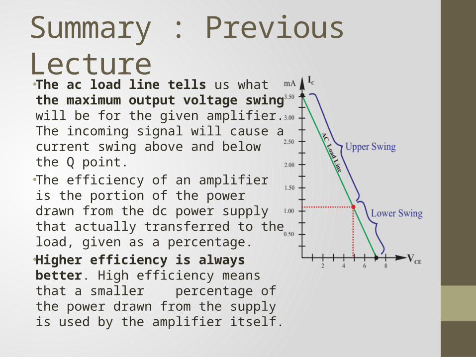
Summary : Previous Lecture• The ac load line tells us what the
maximum output voltage swing will be for the given amplifier. The incoming signal will cause a current swing above and below the Q point.
• The efficiency of an amplifier is the portion of the power drawn from the dc power supply that actually transferred to the load, given as a percentage.
• Higher efficiency is always better. High efficiency means that a smaller percentage of the power drawn from the supply is used by the amplifier itself.
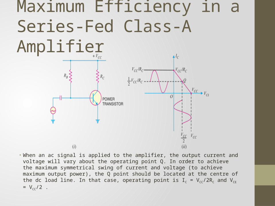
Maximum Efficiency in a Series-Fed Class-A Amplifier
• When an ac signal is applied to the amplifier, the output current and voltage will vary about the operating point Q. In order to achieve the maximum symmetrical swing of current and voltage (to achieve maximum output power), the Q point should be located at the centre of the dc load line. In that case, operating point is IC = VCC/2RC and VCE = VCC/2 .
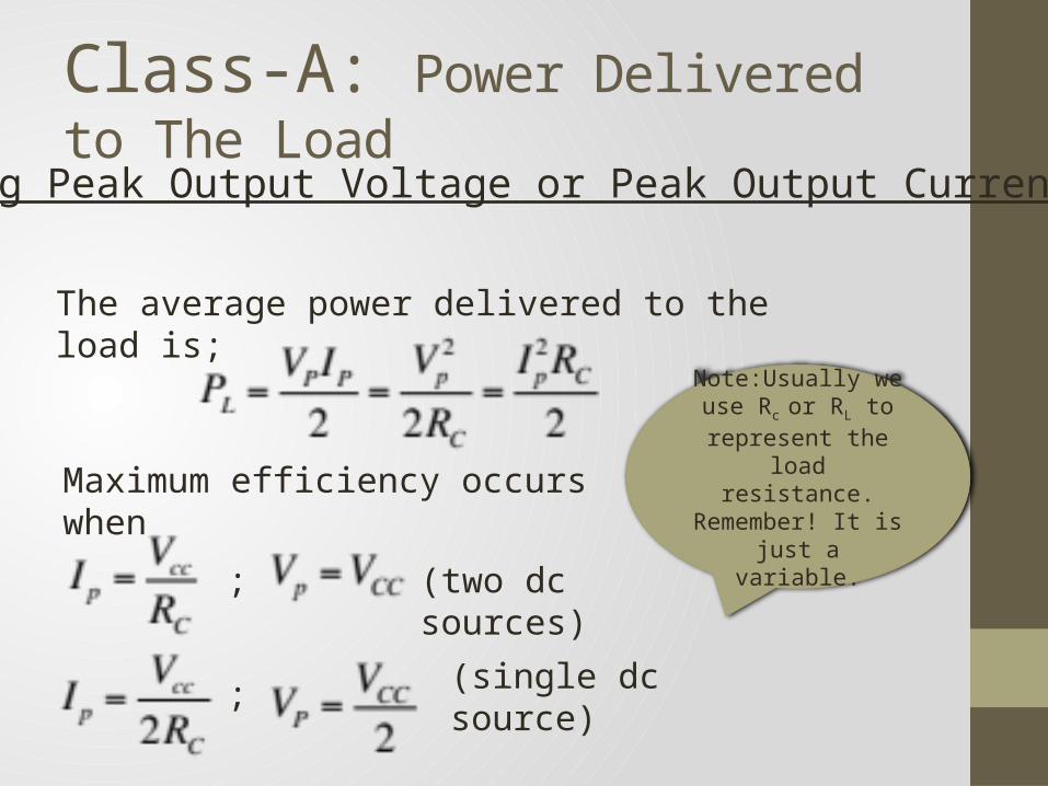
Class-A: Power Delivered to The Load
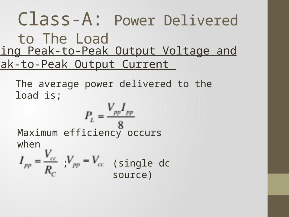
The average power delivered to the load is;
Maximum efficiency occurs when
(two dc sources)
(single dc source)
;
;
Using Peak Output Voltage or Peak Output Current
Note:Usually we use Rc
or RL to represent the load resistance.
Remember! It is just a variable.
Class-A: Power Delivered to The Load
The average power delivered to the load is;
Maximum efficiency occurs when
(single dc source);
Using Peak-to-Peak Output Voltage andPeak-to-Peak Output Current
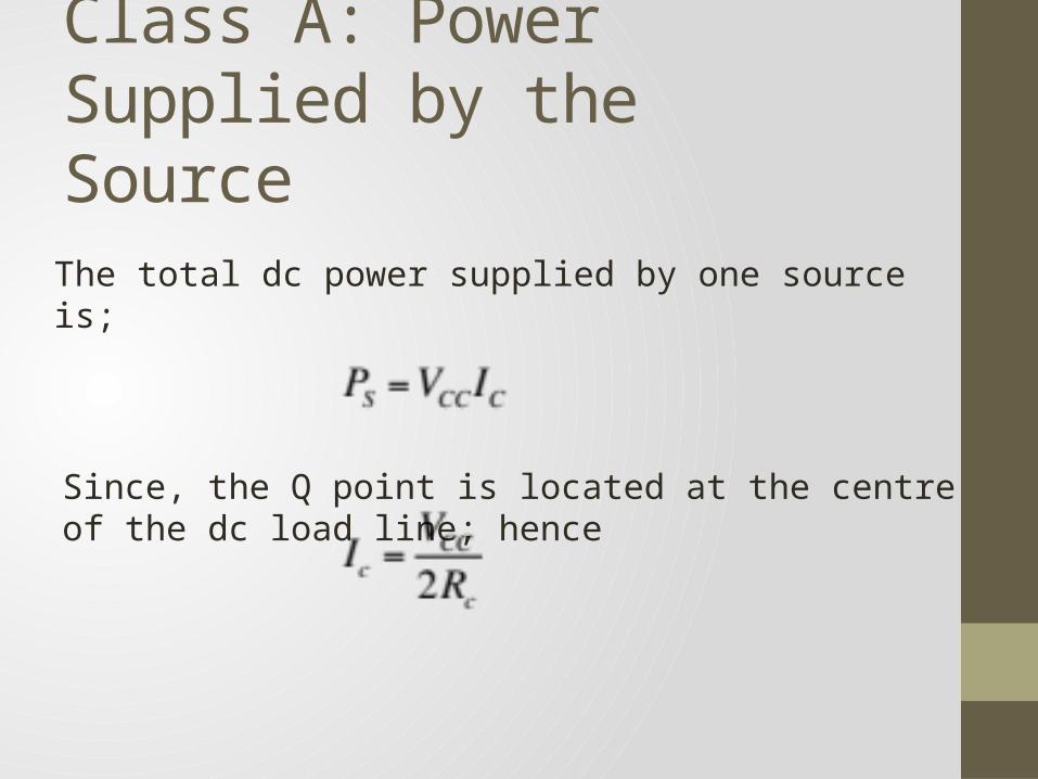
Class A: Power Supplied by the Source
The total dc power supplied by one source is;
Since, the Q point is located at the centre of the dc load line; hence
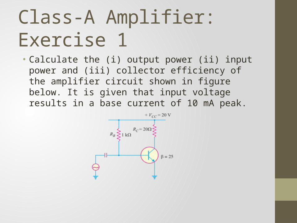
Class-A Amplifier: Exercise 1• Calculate the (i) output power (ii) input power and (iii)
collector efficiency of the amplifier circuit shown in figure below. It is given that input voltage results in a base current of 10 mA peak.
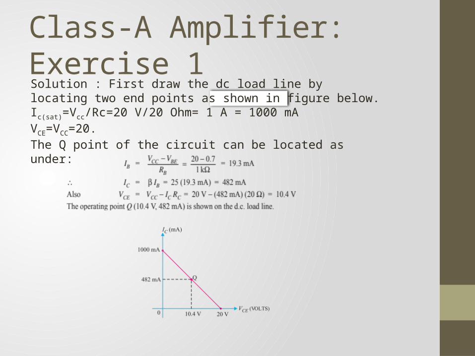
Class-A Amplifier: Exercise 1Solution : First draw the dc load line by locating two end points as shown in figure below.Ic(sat)=Vcc/Rc=20 V/20 Ohm= 1 A = 1000 mAVCE=VCC=20. The Q point of the circuit can be located as under:
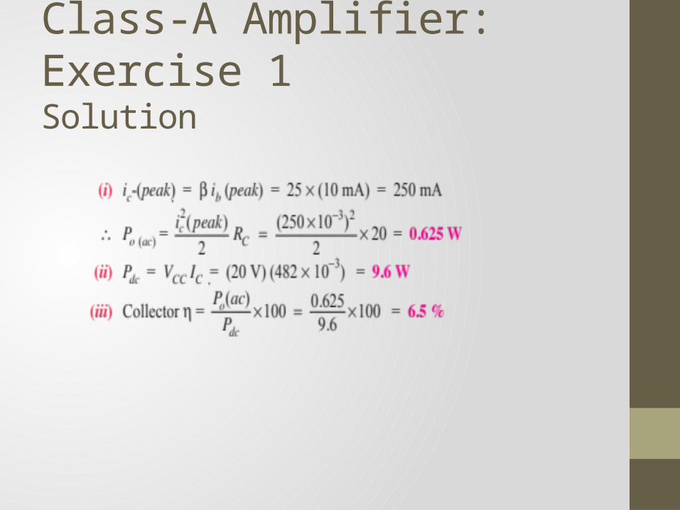
Class-A Amplifier: Exercise 1Solution
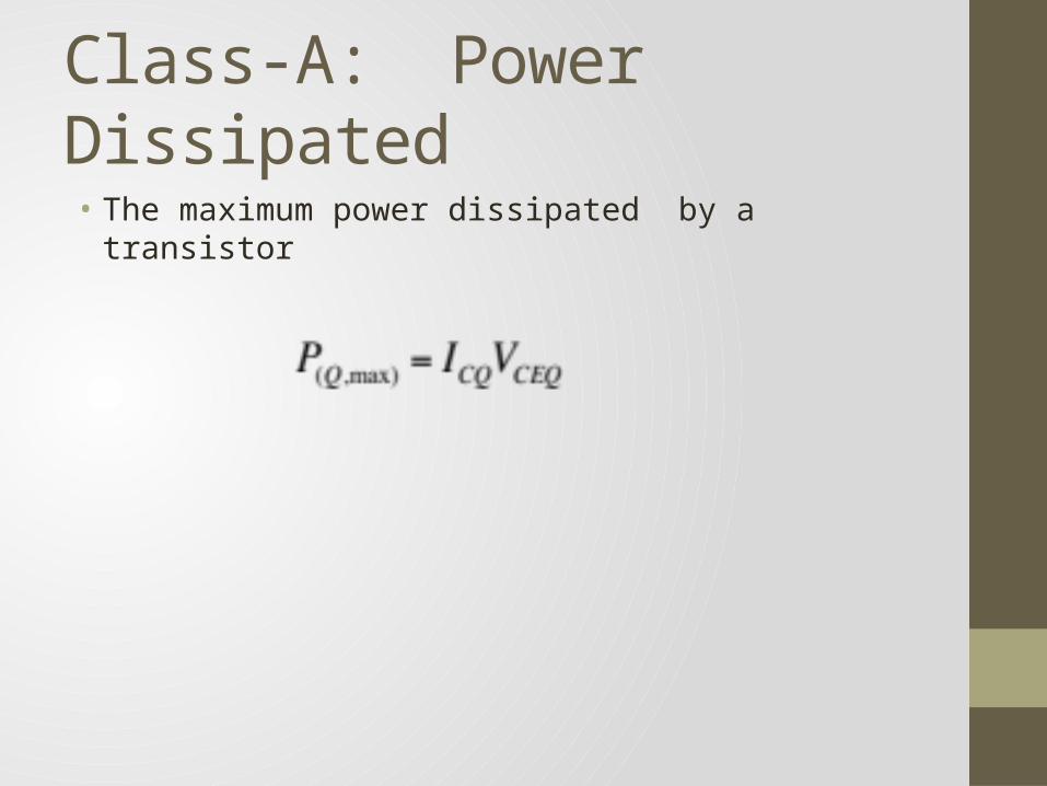
Class-A: Power Dissipated• The maximum power dissipated by a transistor
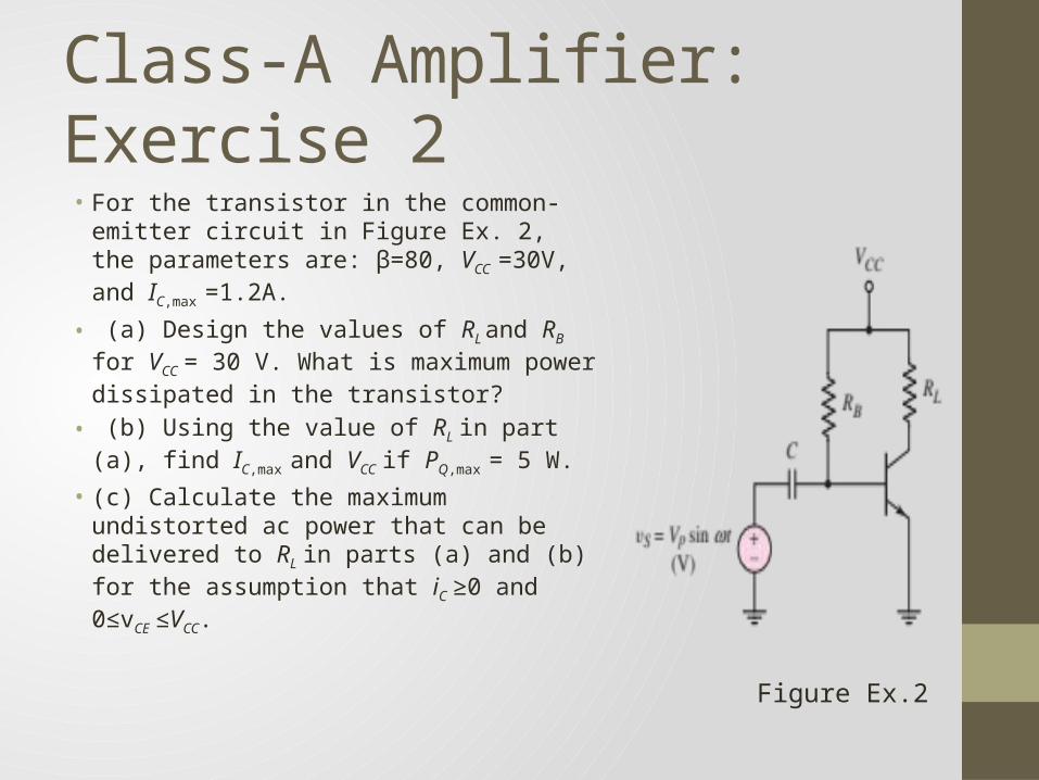
Class-A Amplifier: Exercise 2• For the transistor in the common-emitter
circuit in Figure Ex. 2, the parameters are: β=80, VCC =30V, and IC,max =1.2A.
• (a) Design the values of RL and RB for VCC = 30 V. What is maximum power dissipated in the transistor?
• (b) Using the value of RL in part (a), find IC,max and VCC if PQ,max = 5 W.
• (c) Calculate the maximum undistorted ac power that can be delivered to RL in parts (a) and (b) for the assumption that iC ≥0 and 0≤vCE ≤VCC.
Figure Ex.2
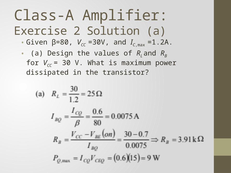
Class-A Amplifier: Exercise 2 Solution (a)
• Given β=80, VCC =30V, and IC,max =1.2A.
• (a) Design the values of RL and RB for VCC = 30 V. What is maximum power dissipated in the transistor?
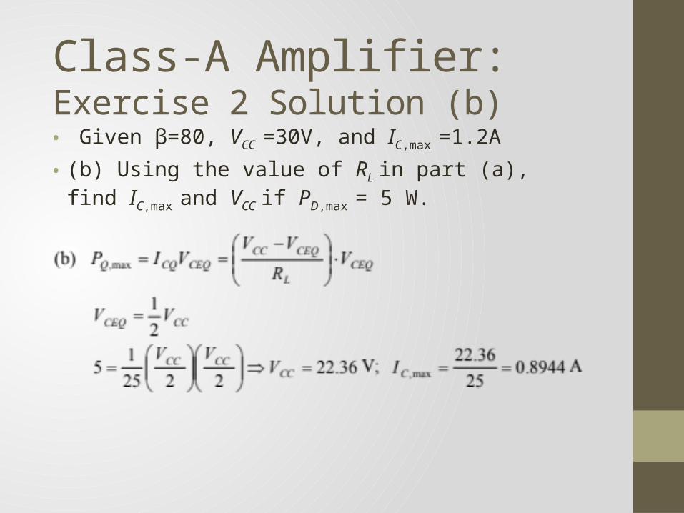
Class-A Amplifier: Exercise 2 Solution (b)• Given β=80, VCC =30V, and IC,max =1.2A
• (b) Using the value of RL in part (a), find IC,max and VCC if PD,max = 5 W.
Class-A Amplifier: Exercise 2 Solution (c)
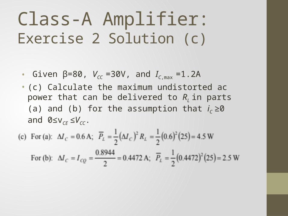
• Given β=80, VCC =30V, and IC,max =1.2A• (c) Calculate the maximum undistorted ac power that can
be delivered to RL in parts (a) and (b) for the assumption that iC ≥0 and 0≤vCE ≤VCC.
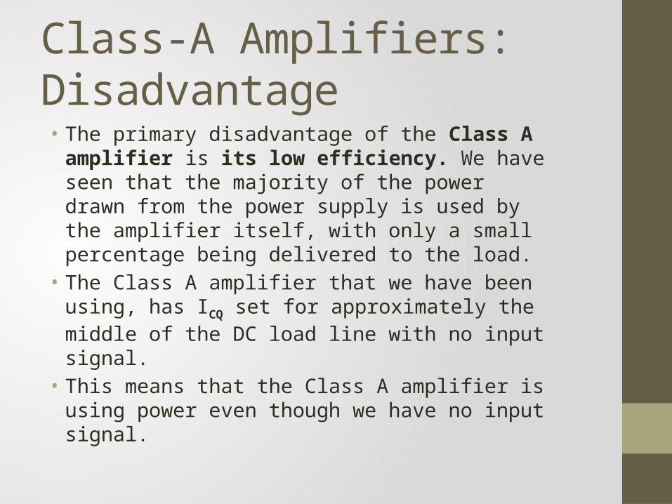
Class-A Amplifiers: Disadvantage• The primary disadvantage of the Class A amplifier is its
low efficiency. We have seen that the majority of the power drawn from the power supply is used by the amplifier itself, with only a small percentage being delivered to the load.
• The Class A amplifier that we have been using, has ICQ set for approximately the middle of the DC load line with no input signal.
• This means that the Class A amplifier is using power even though we have no input signal.
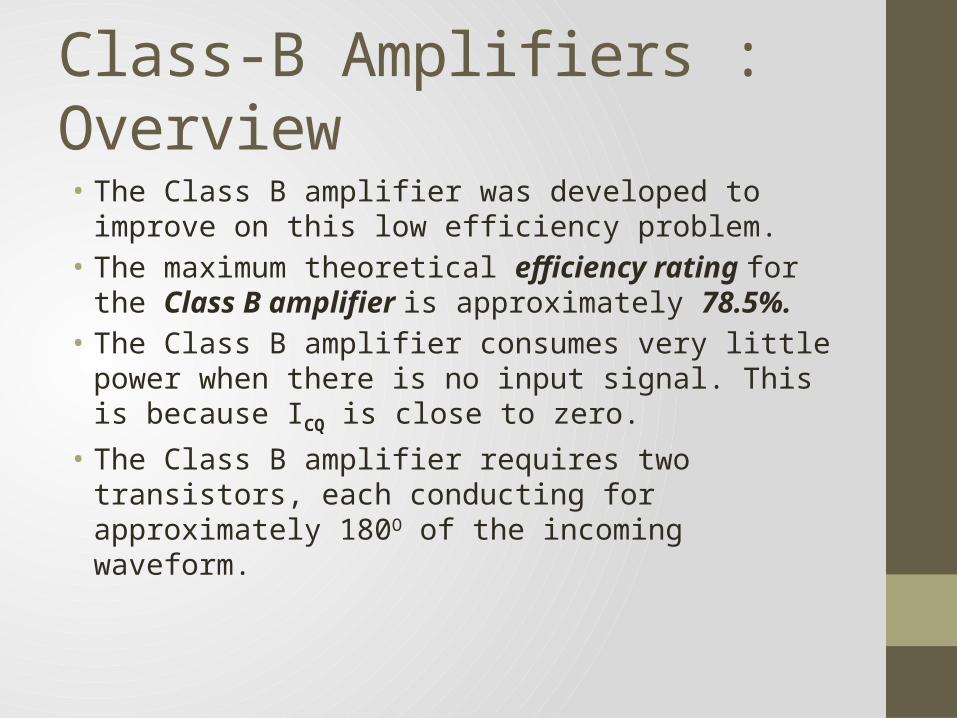
Class-B Amplifiers : Overview • The Class B amplifier was developed to improve on this low
efficiency problem. • The maximum theoretical efficiency rating for the Class B
amplifier is approximately 78.5%. • The Class B amplifier consumes very little power when there is
no input signal. This is because ICQ is close to zero. • The Class B amplifier requires two transistors, each conducting
for approximately 180O of the incoming waveform.
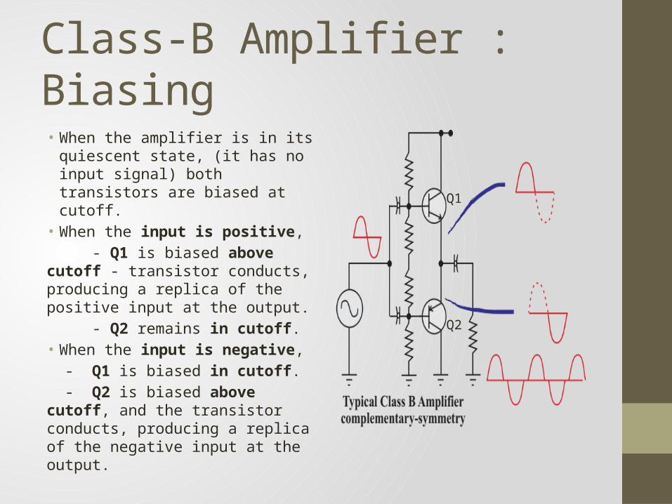
Class-B Amplifier : Biasing
• When the amplifier is in its quiescent state, (it has no input signal) both transistors are biased at cutoff.
• When the input is positive, - Q1 is biased above cutoff - transistor conducts, producing a replica of the positive input at the output. - Q2 remains in cutoff. • When the input is negative, - Q1 is biased in cutoff. - Q2 is biased above cutoff, and the transistor conducts, producing a replica of the negative input at the output.
Q1
Q2
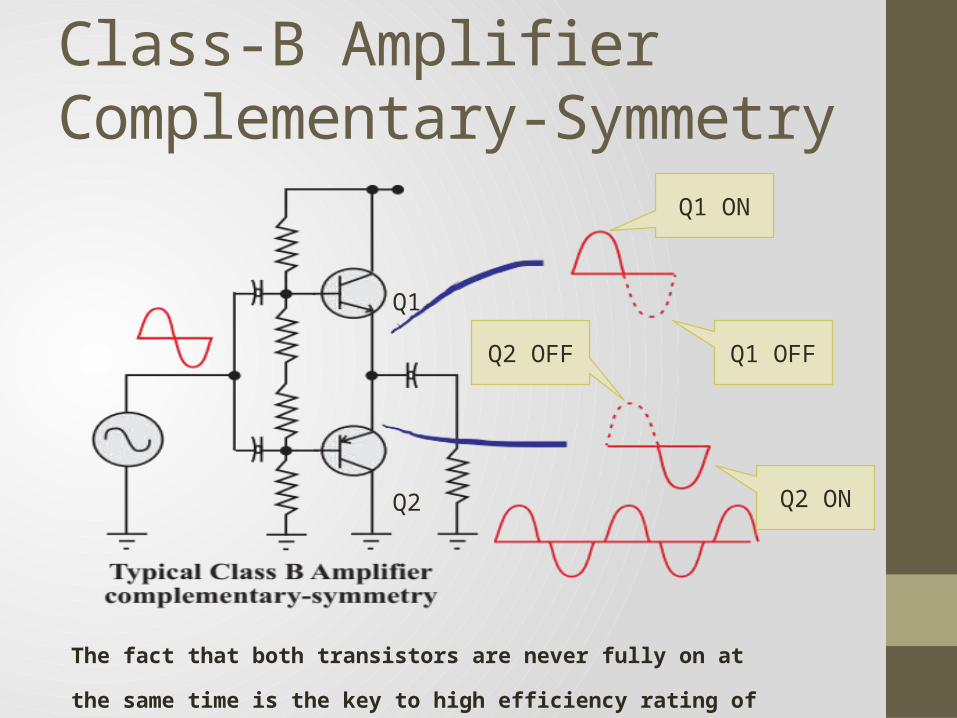
Class-B Amplifier Complementary-Symmetry
Q1
Q2
Q1 OFF
Q1 ON
Q2 ON
Q2 OFF
The fact that both transistors are never fully on at the same time is the key to
high efficiency rating of this amplifier.
Class-B : DC Operating Characteristics• Matched transistors should be used in Class B
amplifiers because any difference in the operating characteristics of individual transistors will cause non-linearity and output distortion.
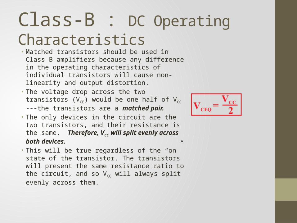
• The voltage drop across the two transistors (VCE) would be one half of VCC ---the transistors are a matched pair.
• The only devices in the circuit are the two transistors, and their resistance is the same. Therefore, VCC will split evenly across both devices.
• This will be true regardless of the “on” state of the transistor. The transistors will present the same resistance ratio to the circuit, and so VCC will always split evenly across them.
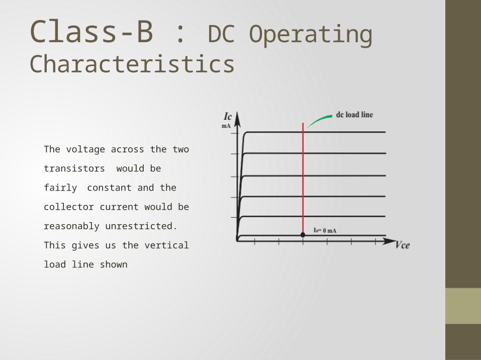
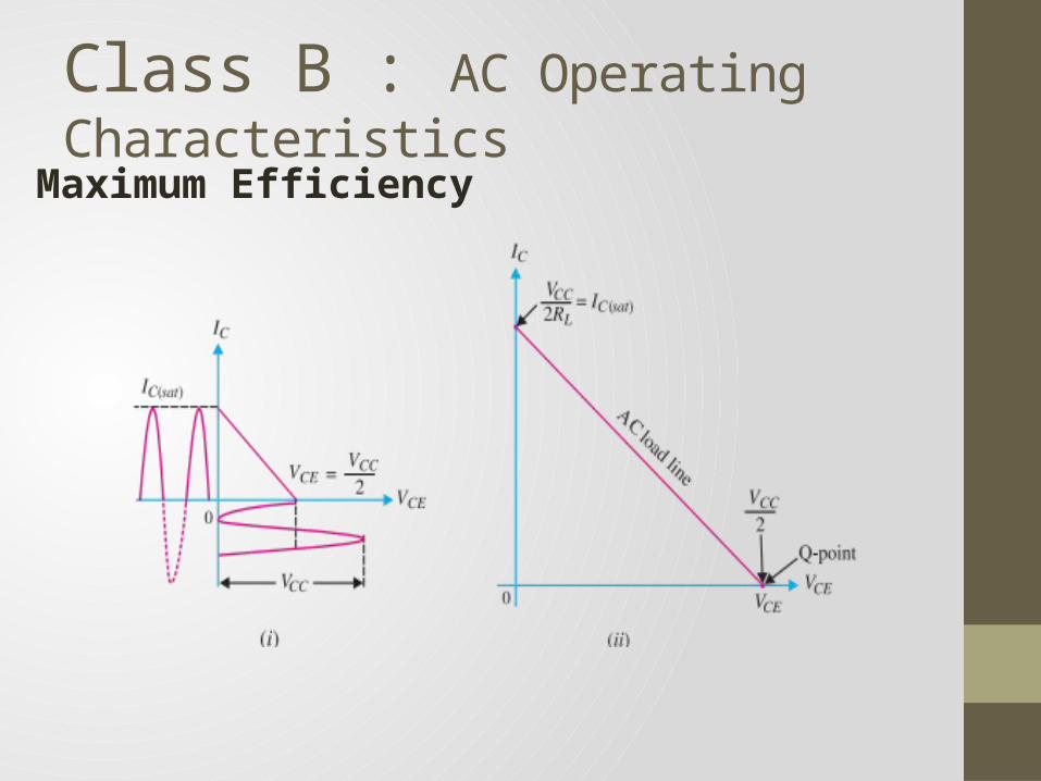
The voltage across the two transistors
would be fairly constant and the
collector current would be reasonably
unrestricted. This gives us the vertical
load line shown
Class-B : DC Operating Characteristics
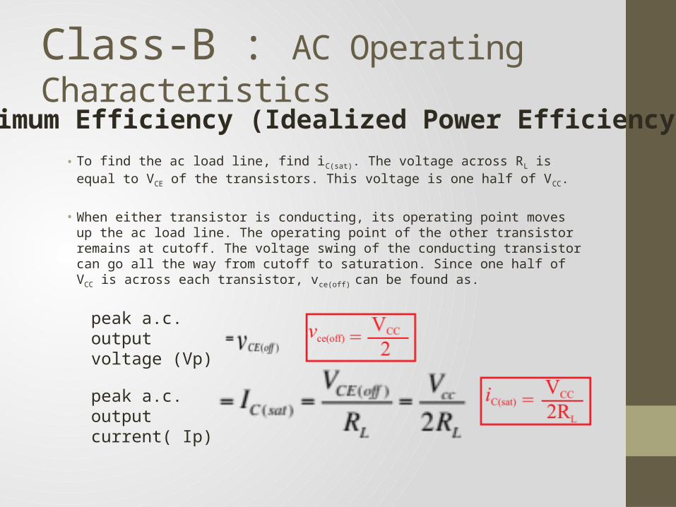
• To find the ac load line, find iC(sat). The voltage across RL is equal to VCE of the transistors. This voltage is one half of VCC.
• When either transistor is conducting, its operating point moves up the ac load line. The operating point of the other transistor remains at cutoff. The voltage swing of the conducting transistor can go all the way from cutoff to saturation. Since one half of VCC is across each transistor, vce(off) can be found as.
Class-B : AC Operating Characteristics
peak a.c. output voltage (Vp)
peak a.c. output current( Ip)
Maximum Efficiency (Idealized Power Efficiency)
Class B : AC Operating Characteristics
Maximum Efficiency
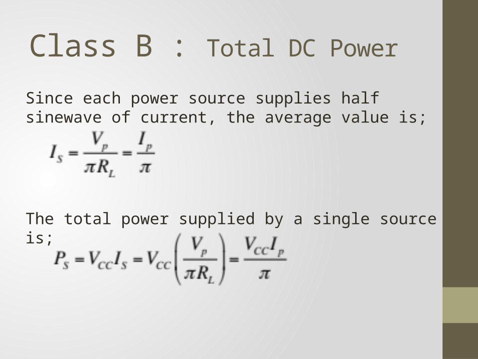
Since each power source supplies half sinewave of current, the average value is;
The total power supplied by a single source is;
Class B : Total DC Power
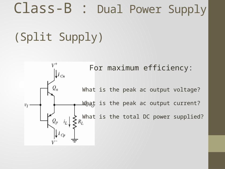
Class-B : Dual Power Supply (Split Supply)
What is the peak ac output voltage?
What is the peak ac output current?
What is the total DC power supplied?
For maximum efficiency:
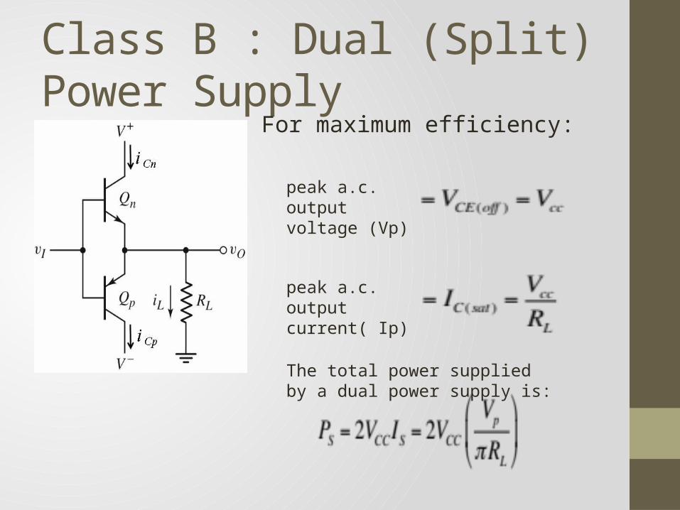
Class B : Dual (Split) Power Supply
For maximum efficiency:
peak a.c. output voltage (Vp)
peak a.c. output current( Ip)
The total power supplied by a dual power supply is:
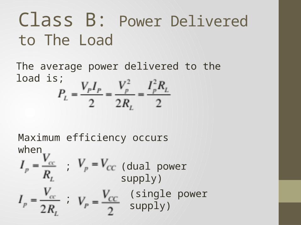
Class B: Power Delivered to The Load
The average power delivered to the load is;
Maximum efficiency occurs when
(dual power supply)
(single power supply)
;
;
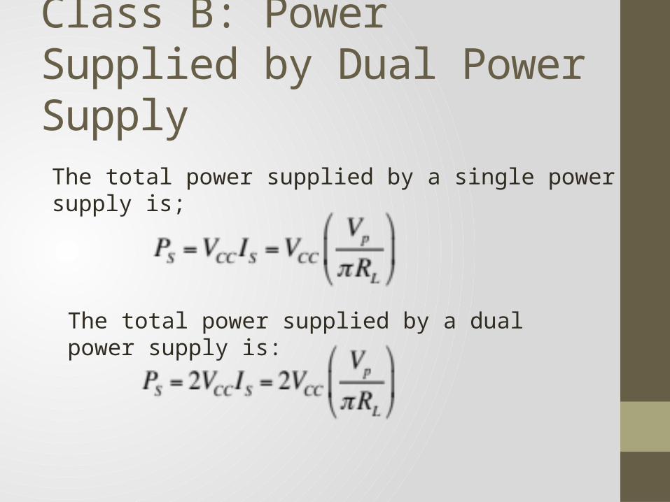
Class B: Power Supplied by Dual Power Supply
The total power supplied by a single power supply is;
The total power supplied by a dual power supply is:
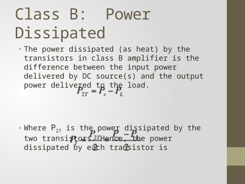
Class B: Power Dissipated• The power dissipated (as heat) by the transistors in class B
amplifier is the difference between the input power delivered by DC source(s) and the output power delivered to the load.
• Where P2T is the power dissipated by the two transistors. Hence, the power dissipated by each transistor is
Class B Amplifier: Exercise 3
• For a class B amplifier using a supply of VCC = 12V and driving a load of 8Ω, determine
(i) maximum load power (ii) DC. input power (iii) efficiency.
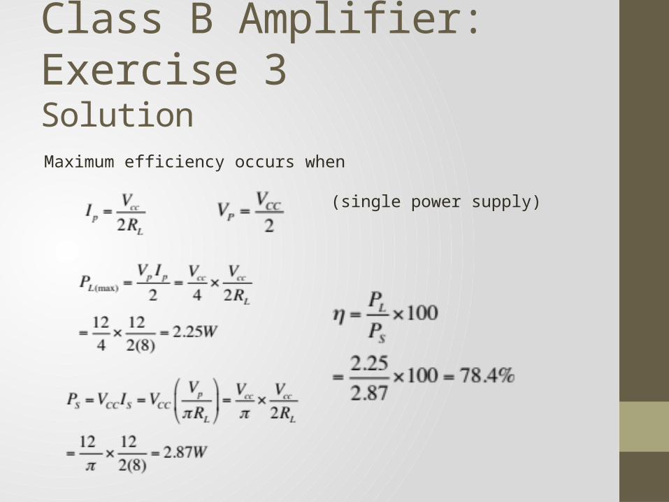
Class B Amplifier: Exercise 3Solution
Maximum efficiency occurs when
(single power supply)
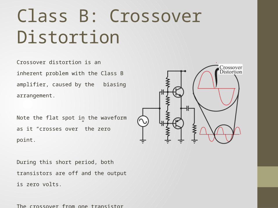
Class B: Crossover Distortion
Crossover distortion is an inherent problem with
the Class B amplifier, caused by the biasing
arrangement.
Note the flat spot in the waveform as it “crosses
over” the zero point.
During this short period, both transistors are off
and the output is zero volts.
The crossover from one transistor to the other is
not instantaneous. The “on transistor” turns off
before the “off transistor” turns on.
This can be eliminated by biasing the transistors
slightly above cutoff.
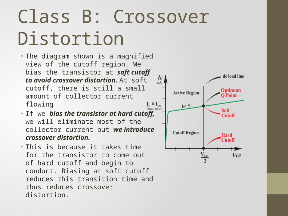
Class B: Crossover Distortion• The diagram shown is a magnified
view of the cutoff region. We bias the transistor at soft cutoff to avoid crossover distortion. At soft cutoff, there is still a small amount of collector current flowing
• If we bias the transistor at hard cutoff, we will eliminate most of the collector current but we introduce crossover distortion.
• This is because it takes time for the transistor to come out of hard cutoff and begin to conduct. Biasing at soft cutoff reduces this transition time and thus reduces crossover distortion.
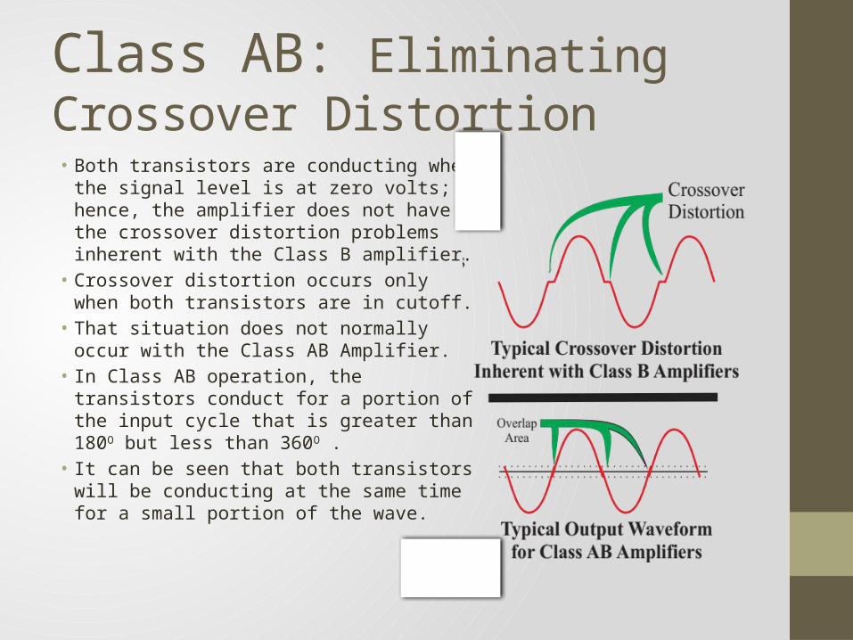
Class AB: Eliminating Crossover Distortion• Both transistors are conducting when the
signal level is at zero volts; hence, the amplifier does not have the crossover distortion problems inherent with the Class B amplifier.
• Crossover distortion occurs only when both transistors are in cutoff.
• That situation does not normally occur with the Class AB Amplifier.
• In Class AB operation, the transistors conduct for a portion of the input cycle that is greater than 180O but less than 360O .
• It can be seen that both transistors will be conducting at the same time for a small portion of the wave.