
Circuto de Chip 5846
159
MLS Driver Chip Set Technical Manual MF1030-02
-
Upload
angela-fernandez-montero -
Category
Documents
-
view
29 -
download
3
Transcript of Circuto de Chip 5846
MLS Driver C
hip Set
Technica
l Manual
MF1030-02
“Seiko Epson is neither licensed nor authorized to license its customers under one or more patents held byMotif Corporation to use this integrated circuit in the manufacture of liquid crystal display modules. Suchlicense, however, may be obtained directly from MOTIF by writing to: Motif, Inc., c/o In Focus Systems, Inc.,27700A SW Parkway Avenue, Wilsonville, OR 97070-9215, Attention: Vice President CorporateDevelopment.”
NOTICE
No parts of this material may be reproduced or duplicated in any form or by any means without the writtenpermission of Seiko Epson. Seiko Epson reserves the right to make changes to this material without notice.Seiko Epson does not assume any liability of any kind aristing out of any inaccuracies contained in thismaterial or due to its application or use in any product or circuit and, further, there is no representation thatthis material is applicable to products requiring high level reliability, such as, medical products. Moreover,no license to any intellectual property rights is granted by implication or otherwise, and there is norepresentation or warranty that anything made in accordance with this material will be free from any patentor copyright infringement of a third party. This material or portions thereof may contain technology or thesubject relating to strategic products under the control of the Foreign Exchange and Foreign Trade ControlLaw of Japan and may require an export licence from teh Ministry of International Trade and Industry or otherapproval from another government agency.
© Seiko Epson Corporation 1998 All right reserved.

CONTENTS
MLS Driver Chip Set EPSON iTechnical Manual
CONTENTS
SED1360 Series . . . . . . . . . . . . . . . . . . . . . . . . . . . . . . . . . 1-1
SED1580 . . . . . . . . . . . . . . . . . . . . . . . . . . . . . . . . . . . . . . 2-1
SED1590 . . . . . . . . . . . . . . . . . . . . . . . . . . . . . . . . . . . . . . 3-1
SED1750 . . . . . . . . . . . . . . . . . . . . . . . . . . . . . . . . . . . . . . 4-1
SED1751 . . . . . . . . . . . . . . . . . . . . . . . . . . . . . . . . . . . . . . 5-1
SCI7500F0A . . . . . . . . . . . . . . . . . . . . . . . . . . . . . . . . . . . . 6-1
MLS Drive Method LCD Chp Set
MLS Driver Chip Set EPSON 1Technical Manual
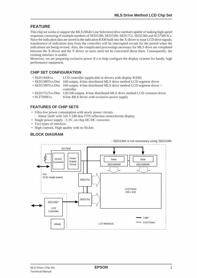
FEATUREThis chip set works to support the MLS (Multi Line Selection) drive method capable of making high-speedresponses consisting of multiple numbers of SED1580, SED1590, SED1751, SED1360 and SCI7500 ICs.Since the indication data are stored in the indication RAM built into the X-driver to issue LCD drive signals,transference of indication data from the controller will be interrupted except for the period when theindications are being revised. Also, the complicated processings necessary for MLS drive are completedbetween the X-driver and the Y-driver so users need not be concerned about them. Consequently, theexisting interface is usable.Moreover, we are preparing exclusive power ICs to help configure the display systems for handy, highperformance equipment.
CHIP SET CONFIGURATION• SED1360F0A LCD controller (applicable to drivers with display RAM)• SED1580T0A/D0B 160-output, 4-line distributed MLS drive method LCD segment driver• SED1590T0A/D0B 160-output, 4-line distributed MLS drive method LCD segment driver +
controller• SED1751T0A/D0B 120/100-output, 4-line distributed MLS drive method LCD common driver• SCI7500F0A 4-line MLS driver with exclusive power supply
FEATURES OF CHIP SETS• Ultra-low power consumption with newly power circuits.
– About 5mW with 320 × 240 dots FTN reflection monochrome display.• Single power supply : 3.3V, on chip DC/DC converter.• Two types of interface.• High contrast, High quality with no flicker.
BLOCK DIAGRAM
: SED1360 is not necessary using SED1590.
RAM RAM
SED1580/90SED1580/90
LCD Panel320 x 240
SED1751
SED1751
LCD MODULEVRAM
SED1360 *
LCDController
PowerSupplyCircuit
DC/DCConverter
SCI7500
VDD
(3.3V single power)
Logic
LCD Power
MLS Drive Method LCD Chp Set
2 EPSON MLS Driver Chip SetTechnical Manual
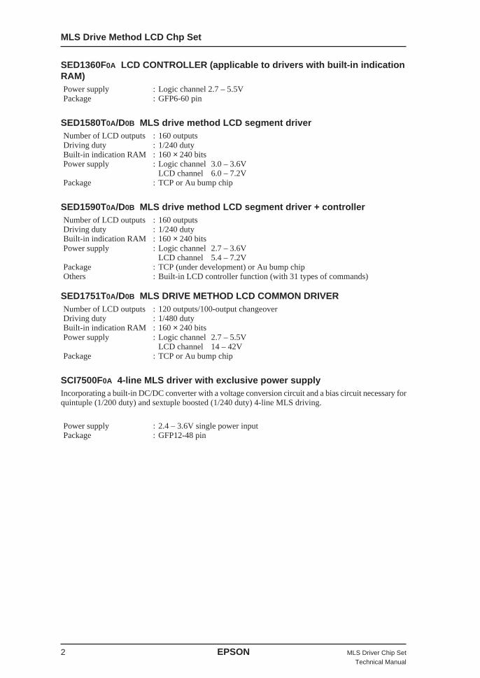
SED1360F0A LCD CONTROLLER (applicable to drivers with built-in indicationRAM)Power supply : Logic channel 2.7 – 5.5VPackage : GFP6-60 pin
SED1580T0A/D0B MLS drive method LCD segment driverNumber of LCD outputs : 160 outputsDriving duty : 1/240 dutyBuilt-in indication RAM : 160 × 240 bitsPower supply : Logic channel 3.0 – 3.6V
LCD channel 6.0 – 7.2VPackage : TCP or Au bump chip
SED1590T0A/D0B MLS drive method LCD segment driver + controllerNumber of LCD outputs : 160 outputsDriving duty : 1/240 dutyBuilt-in indication RAM : 160 × 240 bitsPower supply : Logic channel 2.7 – 3.6V
LCD channel 5.4 – 7.2VPackage : TCP (under development) or Au bump chipOthers : Built-in LCD controller function (with 31 types of commands)
SED1751T0A/D0B MLS DRIVE METHOD LCD COMMON DRIVERNumber of LCD outputs : 120 outputs/100-output changeoverDriving duty : 1/480 dutyBuilt-in indication RAM : 160 × 240 bitsPower supply : Logic channel 2.7 – 5.5V
LCD channel 14 – 42VPackage : TCP or Au bump chip
SCI7500F0A 4-line MLS driver with exclusive power supplyIncorporating a built-in DC/DC converter with a voltage conversion circuit and a bias circuit necessary forquintuple (1/200 duty) and sextuple boosted (1/240 duty) 4-line MLS driving.
Power supply : 2.4 – 3.6V single power inputPackage : GFP12-48 pin

SED1360 Series
SED1360 Series
MLS Driver Chip Set EPSON iTechnical Manual
Contents
INTRODUCTION........................................................................................................................... 1-1
FEATURES ................................................................................................................................... 1-1
OVERVIEW DESCRIPTION ......................................................................................................... 1-2
PINOUT DIAGRAM ....................................................................................................................... 1-5
PIN DESCRIPTION....................................................................................................................... 1-8
D.C. CHARACTERISTICS .......................................................................................................... 1-11
A.C. CHARACTERISTICS .......................................................................................................... 1-14
OPERATION DESCRIPTION ..................................................................................................... 1-19
OSCILLATION DESCRIPTION ................................................................................................... 1-25
COMMAND DESCRIPTION........................................................................................................ 1-26
ERRORTA................................................................................................................................... 1-29
NOTICE ....................................................................................................................................... 1-29

SED1360 Series
MLS Driver Chip Set EPSON 1–1Technical Manual
INTRODUCTIONScopeThis is the Functional Specification for SED1360 3.3 V Ultra Low Power LCD Controller Chip.
Objectives(1) To specify functions and interface requirements of the chip.(2) To allow review of the functions of the chip, as a preliminary specification.
FEATURESTechnology• ultra low power CMOS process• 3.3 volt operation• chip supply with aluminum pad• 64 pin QFP6 surface mount package
System• Direct connection to the 68 family CPUs.• minimum CPU Interface pin count.• no buffers are required in a 3.3 V-System.• internal oscillator with external Capacitance and Resistance, or external oscillator for a low frequency
input source.• interfaces to 64 kb and, or 256 kb SRAMs.• controls Seiko Epson’s RAM integrated Segment Drivers.• self-controlled Doze Mode.• optimized Hardware for low to medium resolution LCDs.• ultra low power consumption.

SED1360 Series
1–2 EPSON MLS Driver Chip SetTechnical Manual
OVERVIEW DESCRIPTIONSED1360 is an ultra low power 3.3 V LCD controller which is optimized to drive low to medium resolutionLCD panels. SED1360 can interface to the 68 family CPUs in the Port Peripheral Timing.
Typical System Block DiagramThe following figure shows typical system implementation with SED1360.
Figure 1. Typical System Block Diagram
Y.Dr. LCD Panel
SRAM
LCD Module(Consisting of RAM Drivers)
Display Subsystem
SED136068HC11
D[0:7]ECSDT/CM
SLEEPRESET
VD[0:7]
VA[0:14]VCS[0:1]VOEVR/W
YDLPXD[0:7]XSCLUFRDOFF RAM Driver
SED1360 Series
MLS Driver Chip Set EPSON 1–3Technical Manual
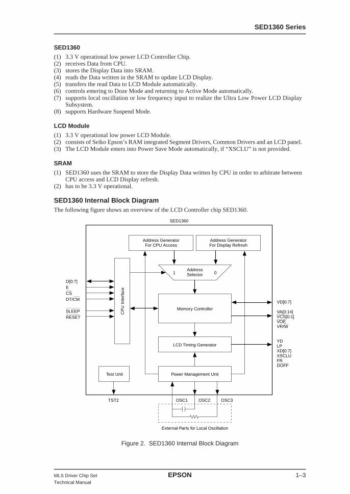
SED1360
(1) 3.3 V operational low power LCD Controller Chip.(2) receives Data from CPU.(3) stores the Display Data into SRAM.(4) reads the Data written in the SRAM to update LCD Display.(5) transfers the read Data to LCD Module automatically.(6) controls entering to Doze Mode and returning to Active Mode automatically.(7) supports local oscillation or low frequency input to realize the Ultra Low Power LCD Display
Subsystem.(8) supports Hardware Suspend Mode.
LCD Module
(1) 3.3 V operational low power LCD Module.(2) consists of Seiko Epson’s RAM integrated Segment Drivers, Common Drivers and an LCD panel.(3) The LCD Module enters into Power Save Mode automatically, if “XSCLU” is not provided.
SRAM
(1) SED1360 uses the SRAM to store the Display Data written by CPU in order to arbitrate betweenCPU access and LCD Display refresh.
(2) has to be 3.3 V operational.
SED1360 Internal Block DiagramThe following figure shows an overview of the LCD Controller chip SED1360.
Address GeneratorFor CPU Access
Address GeneratorFor Display Refresh
AddressSelector
Memory Controller
SED1360
LCD Timing Generator
CP
U In
terf
ace
Power Management Unit
External Parts for Local Oscillation
OSC1TST2 OSC2 OSC3
Test Unit
1 0
D[0:7]ECSDT/CM
SLEEPRESET
VD[0:7]
VA[0:14]VCS[0:1]VOEVR/W
YDLPXD[0:7]XSCLUFRDOFF
Figure 2. SED1360 Internal Block Diagram
SED1360 Series
1–4 EPSON MLS Driver Chip SetTechnical Manual
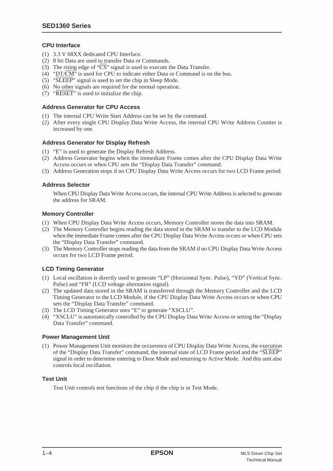
CPU Interface
(1) 3.3 V 68XX dedicated CPU Interface.(2) 8 bit Data are used to transfer Data or Commands.(3) The rising edge of “CS” signal is used to execute the Data Transfer.(4) “DT/CM” is used for CPU to indicate either Data or Command is on the bus.(5) “SLEEP” signal is used to set the chip in Sleep Mode.(6) No other signals are required for the normal operation.(7) “RESET” is used to initialize the chip.
Address Generator for CPU Access
(1) The internal CPU Write Start Address can be set by the command.(2) After every single CPU Display Data Write Access, the internal CPU Write Address Counter is
increased by one.
Address Generator for Display Refresh
(1) “E” is used to generate the Display Refresh Address.(2) Address Generator begins when the immediate Frame comes after the CPU Display Data Write
Access occurs or when CPU sets the “Display Data Transfer” command.(3) Address Generation stops if no CPU Display Data Write Access occurs for two LCD Frame period.
Address Selector
When CPU Display Data Write Access occurs, the internal CPU Write Address is selected to generatethe address for SRAM.
Memory Controller
(1) When CPU Display Data Write Access occurs, Memory Controller stores the data into SRAM.(2) The Memory Controller begins reading the data stored in the SRAM to transfer to the LCD Module
when the immediate Frame comes after the CPU Display Data Write Access occurs or when CPU setsthe “Display Data Transfer” command.
(3) The Memory Controller stops reading the data from the SRAM if no CPU Display Data Write Accessoccurs for two LCD Frame period.
LCD Timing Generator
(1) Local oscillation is directly used to generate “LP” (Horizontal Sync. Pulse), “YD” (Vertical Sync.Pulse) and “FR” (LCD voltage alternation signal).
(2) The updated data stored in the SRAM is transferred through the Memory Controller and the LCDTiming Generator to the LCD Module, if the CPU Display Data Write Access occurs or when CPUsets the “Display Data Transfer” command.
(3) The LCD Timing Generator uses “E” to generate “XSCLU”.(4) “XSCLU” is automatically controlled by the CPU Display Data Write Access or setting the “Display
Data Transfer” command.
Power Management Unit
(1) Power Management Unit monitors the occurrence of CPU Display Data Write Access, the executionof the “Display Data Transfer” command, the internal state of LCD Frame period and the “SLEEP”signal in order to determine entering to Doze Mode and returning to Active Mode. And this unit alsocontrols local oscillation.
Test Unit
Test Unit controls test functions of the chip if the chip is in Test Mode.
SED1360 Series
MLS Driver Chip Set EPSON 1–5Technical Manual
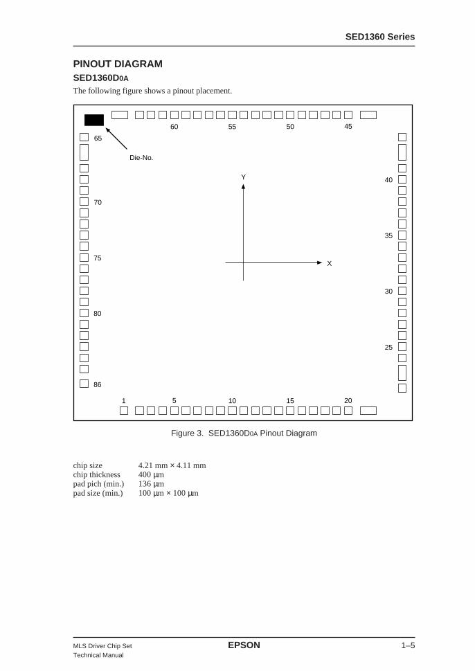
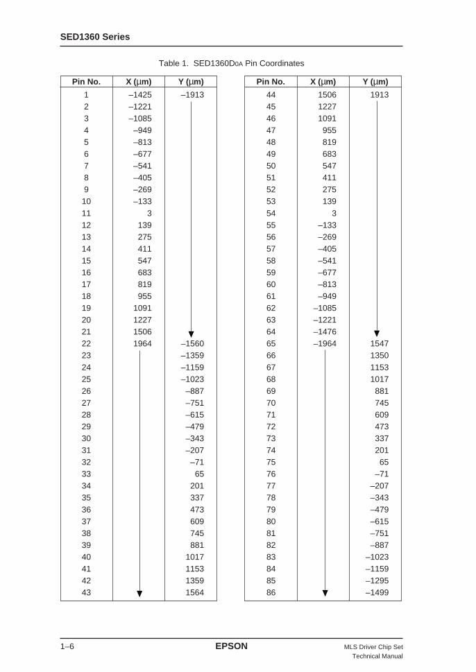
PINOUT DIAGRAMSED1360D0A
The following figure shows a pinout placement.
Figure 3. SED1360D0A Pinout Diagram
chip size 4.21 mm × 4.11 mmchip thickness 400 µmpad pich (min.) 136 µmpad size (min.) 100 µm × 100 µm
65
70
75
80
86
1 5 10 15 20
25
30
35
Y
X
40
45505560
Die-No.
SED1360 Series
1–6 EPSON MLS Driver Chip SetTechnical Manual
Table 1. SED1360D0A Pin Coordinates
44 1506 191345 122746 109147 95548 81949 68350 54751 41152 27553 13954 355 –13356 –26957 –40558 –54159 –67760 –81361 –94962 –108563 –122164 –147665 –1964 154766 135067 115368 101769 88170 74571 60972 47373 33774 20175 6576 –7177 –20778 –34379 –47980 –61581 –75182 –88783 –102384 –115985 –129586 –1499
1 –1425 –19132 –12213 –10854 –9495 –8136 –6777 –5418 –4059 –269
10 –13311 312 13913 27514 41115 54716 68317 81918 95519 109120 122721 150622 1964 –156023 –135924 –115925 –102326 –88727 –75128 –61529 –47930 –34331 –20732 –7133 6534 20135 33736 47337 60938 74539 88140 101741 115342 135943 1564
Pin No. X ( µm) Y (µm)Pin No. X ( µm) Y (µm)
SED1360 Series
MLS Driver Chip Set EPSON 1–7Technical Manual
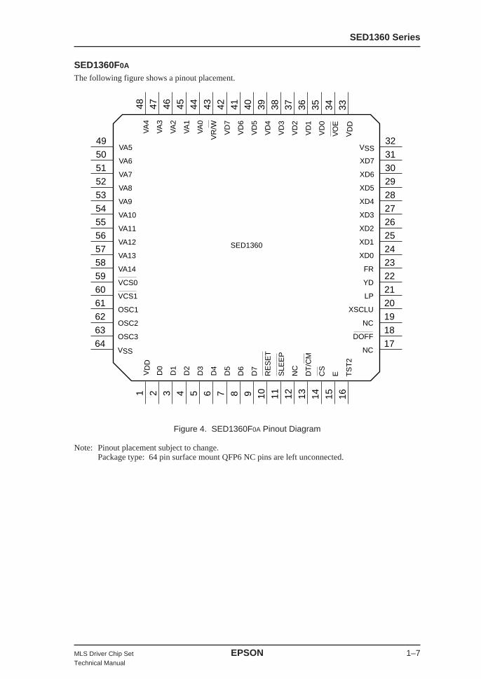
SED1360F0A
The following figure shows a pinout placement.
Figure 4. SED1360F0A Pinout Diagram
Note: Pinout placement subject to change.Package type: 64 pin surface mount QFP6 NC pins are left unconnected.
1 2 3 4 5 6 7 8 9 10 11 12 13 14 15 16
48 47 46 45 44 43 42 41 40 39 38 37 36 35 34 33
49
50
51
52
53
54
55
56
57
58
59
60
61
62
63
64
VA5
VA6
VA7
VA8
VA9
VA10
VA11
VA12
VA13
VA14
VCS0
VCS1
OSC1
OSC2
OSC3
VSS
VSS
XD7
XD6
XD5
XD4
XD3
XD2
XD1
XD0
FR
YD
LP
XSCLU
NC
DOFF
NC
VD
D
D0
D1
D2
D3
D4
D5
D6
D7
RE
SE
T
SLE
EP
NC
DT
/CM
CS
E TS
T2
VA
4
VA
3
VA
2
VA
1
VA
0
VR
/W
VD
7
VD
6
VD
5
VD
4
VD
3
VD
2
VD
1
VD
0
VO
E
VD
D
32
31
30
29
28
27
26
25
24
23
22
21
20
19
18
17
SED1360
SED1360 Series
1–8 EPSON MLS Driver Chip SetTechnical Manual
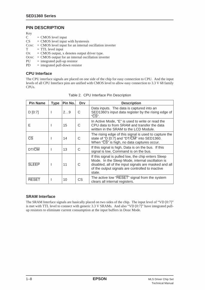
PIN DESCRIPTIONKeyC = CMOS level inputCS = CMOS level input with hysteresisCOSC = CMOS level input for an internal oscillation inverterT = TTL level inputOX = CMOS output, x denotes output driver type.OOSC = CMOS output for an internal oscillation inverterPU = integrated pull-up resistorPD = integrated pull-down resistor
CPU InterfaceThe CPU interface signals are placed on one side of the chip for easy connection to CPU. And the inputlevels of all CPU Interface pins are unified with CMOS level to allow easy connection to 3.3 V 68 familyCPUs.
Table 2. CPU Interface Pin Description
Pin Name Type Pin No. Drv DescriptionData inputs. The data is captured into an
D [0:7] I 2…9 C SED1360’s input data register by the rising edge of“CS”.In Active Mode, “E” is used to write or read the
E I 15 C CPU data to from SRAM and transfer the datawritten in the SRAM to the LCD Module.The rising edge of this signal is used to capture the
CS I 14 C state of “D [0:7] and “DT/CM” into SED1360.When “CS” is high, no data captures occur.
DT/CM I 13 C If this signal is high, Data is on the bus. If thissignal is low, Command is on the bus.If this signal is pulled low, the chip enters SleepMode. In the Sleep Mode, internal oscillation is
SLEEP I 11 C disabled, all of the input signals are masked and allof the output signals are controlled to inactivestate.
RESET I 10 CS The active low “RESET” signal from the systemclears all internal registers.
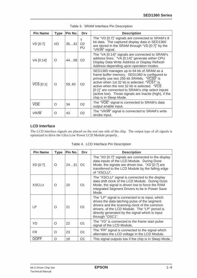
SRAM InterfaceThe SRAM Interface signals are basically placed on two sides of the chip. The input level of “VD [0:7]”is met with TTL level to connect with generic 3.3 V SRAMs. And also “VD [0:7]” have integrated pull-up resistors to eliminate current consumption at the input buffers in Doze Mode.
SED1360 Series
MLS Driver Chip Set EPSON 1–9Technical Manual
Table 3. SRAM Interface Pin Description
Pin Name Type Pin No. Drv Description
T The “VD [0:7]” signals are connected to SRAM’s 8
VD [0:7] I/O 35…42 O2 bit data. The captured display data in SED1360
PU are stored in the SRAM through “VD [0:7]” by the“VR/W” signal.The “VA [0:14]” signals are connected to SRAM’s
VA [0:14] O 44…58 O2 address lines. “VA [0:14]” generate either CPUDisplay Data Write Address or Display RefreshAddress depending upon operation modes.SED1360 manages up to 64 kb of SRAM as aframe buffer memory. SED1360 is configured toprimarily use two 256 kb SRAMs. “VCS0” is
VCS [0:1] O 59, 60 O2 active when 1st 32 kb is selected. “VCS1” isactive when the rest 32 kb is selected. “VCS[0:1]” are connected to SRAM’s chip select inputs(active low). Those signals are inactie (high), if thechip is in Sleep Mode.
VOE O 34 O2 The “VOE” signal is connected to SRAM’s dataoutput enable input.
VR/W O 43 O2 The “VR/W” signal is connected to SRAM’s writestrobe input.
LCD InterfaceThe LCD interface signals are placed on the rest one side of the chip. The output type of all signals isoptimized to drive the Ultra Low Power LCD Module properly.
Pin Name Type Pin No. Drv DescriptionThe “XD [0:7]” signals are connected to the displaydata inputs of the LCD Module. During Doze
XD [0:7] O 24…31 O1 Mode, the signals are driven low. “XD [0:7] aretransferred to the LCD Module by the falling edgeof “XSCLU”.The “XSCLU” signal is connected to the displaydata shift clock of the LCD Module. During Doze
XSCLU O 20 O1 Mode, the signal is driven low to force the RAMintegrated Segment Drivers to be in Power SaveMode.The “LP” signal is connected to te input, whichdrives the data latching pulse of the segment
LP O 21 O1 drivers and the scanning clock of the commondrivers, of the LCD Module. The “LP” period isdirectly generated by the signal which is inputthrough “OSC1”.
YD O 22 O1 The “YD” is connected to the frame start pulsesignal of the LCD Module.
FR O 23 O1 The “FR” signal is connected to the signal whichalternates the LCD voltage in the LCD Module.
DOFF O 18 O1 This signal outputs low if the chip is in Sleep Mode.
Table 4. LCD Interface Pin Description
SED1360 Series
1–10 EPSON MLS Driver Chip SetTechnical Manual
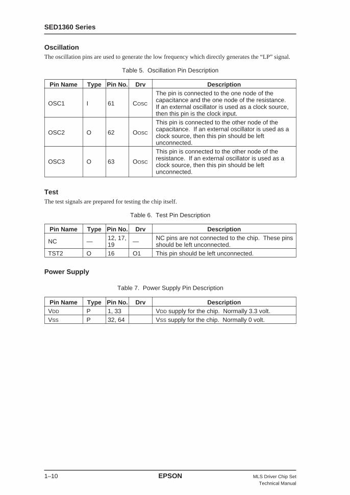
OscillationThe oscillation pins are used to generate the low frequency which directly generates the “LP” signal.
Table 5. Oscillation Pin Description
Pin Name Type Pin No. Drv DescriptionThe pin is connected to the one node of the
OSC1 I 61 COSCcapacitance and the one node of the resistance.If an external oscillator is used as a clock source,then this pin is the clock input.This pin is connected to the other node of the
OSC2 O 62 OOSCcapacitance. If an external oscillator is used as aclock source, then this pin should be leftunconnected.This pin is connected to the other node of the
OSC3 O 63 OOSCresistance. If an external oscillator is used as aclock source, then this pin should be leftunconnected.
TestThe test signals are prepared for testing the chip itself.
Table 6. Test Pin Description
Pin Name Type Pin No. Drv Description
NC — 12, 17, — NC pins are not connected to the chip. These pins19 should be left unconnected.
TST2 O 16 O1 This pin should be left unconnected.
Power Supply
Pin Name Type Pin No. Drv DescriptionVDD P 1, 33 VDD supply for the chip. Normally 3.3 volt.VSS P 32, 64 VSS supply for the chip. Normally 0 volt.
Table 7. Power Supply Pin Description
SED1360 Series
MLS Driver Chip Set EPSON 1–11Technical Manual
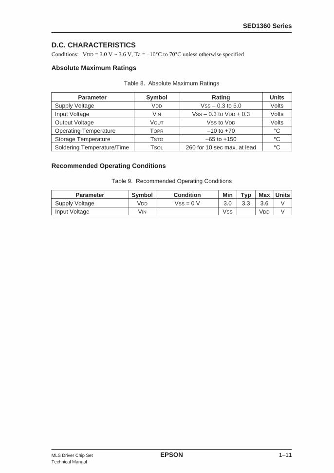
D.C. CHARACTERISTICSConditions: VDD = 3.0 V ~ 3.6 V, Ta = –10°C to 70°C unless otherwise specified
Absolute Maximum Ratings
Table 8. Absolute Maximum Ratings
Parameter Symbol Rating UnitsSupply Voltage VDD VSS – 0.3 to 5.0 VoltsInput Voltage VIN VSS – 0.3 to VDD + 0.3 VoltsOutput Voltage VOUT VSS to VDD VoltsOperating Temperature TOPR –10 to +70 °CStorage Temperature TSTG –65 to +150 °CSoldering Temperature/Time TSOL 260 for 10 sec max. at lead °C
Recommended Operating Conditions
Table 9. Recommended Operating Conditions
Parameter Symbol Condition Min Typ Max UnitsSupply Voltage VDD VSS = 0 V 3.0 3.3 3.6 VInput Voltage VIN VSS VDD V
SED1360 Series
1–12 EPSON MLS Driver Chip SetTechnical Manual
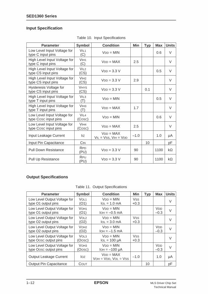
Input Specification
Table 10. Input Specifications
Output Specifications
Table 11. Output Specifications
Parameter Symbol Condition Min Typ Max UnitsLow Level Input Voltage for VIL1 VDD = MIN 0.6 Vtype C input pins (C)High Level Input Voltage for VIH1 VDD = MAX 2.5 Vtype C input pins (C)High Level Input Voltage for VIL2 VDD = 3.3 V 0.5 Vtype CS input pins (CS)High Level Input Voltage for VIH2 VDD = 3.3 V 2.9 Vtype CS input pins (CS)Hysteresis Voltage for VHYS VDD = 3.3 V 0.1 Vtype CS input pins (CS)High Level Input Voltage for VIL3 VDD = MIN 0.5 Vtype T input pins (T)High Level Input Voltage for VIH3 VDD = MAX 1.7 Vtype T input pins (T)Low Level Input Voltage for VIL4 VDD = MIN 0.6 Vtype COSC input pins (COSC)Low Level Input Voltage for VIH4 VDD = MAX 2.5 Vtype COSC input pins (COSC)
Input Leakage Current IIZ VDD = MAX –1.0 1.0 µAVIL = VSS, VIH = VDD
Input Pin Capacitance CIN 10 pF
Pull Down Resistance RPD VDD = 3.3 V 90 1100 kΩ(PU)
Pull Up Resistance RPU VDD = 3.3 V 90 1100 kΩ(PU)
Parameter Symbol Condition Min Typ Max UnitsLow Level Output Voltage for VOL1 VDD = MIN VSS Vtype O1 output pins (O1) IOL = 1.0 mA +0.3Low Level Output Voltage for VOH1 VDD = MIN VDD Vtype O1 output pins (O1) IOH = –0.5 mA –0.3Low Level Output Voltage for VOL2 VDD = MIN VSS Vtype O2 output pins (O2) IOL = 3.0 mA +0.3Low Level Output Voltage for VOH2 VDD = MIN VDD Vtype O2 output pins (O2) IOH = –1.5 mA –0.3Low Level Output Voltage for VOL3 VDD = MIN VSS Vtype OOSC output pins (OOSC) IOL = 100 µA +0.3Low Level Output Voltage for VOH3 VDD = MIN VDD Vtype OOSC output pins (OOSC) IOH = –100 µA –0.3
Output Leakage Current IOZVDD = MAX –1.0 1.0 µAVOH = VDD, VOL = VSS
Output Pin Capacitance COUT 10 pF

SED1360 Series
MLS Driver Chip Set EPSON 1–13Technical Manual
Power Consumption
Parameter Symbol Condition Min Typ Max UnitsCurrent Consumption VDD = 3.3 Vin Active Mode IOP1 tCYCE = 500 ns 5 mAwith CPU write access fOSC = 24 kHz
Current Consumption VDD = 3.3 V
in Active Mode IOP2tCYCE = 500 ns 1 mA
with no CPU write access “CS” = highfOSC = 24 kHz
Current Consumption VDD = 3.3 Vin Doze Mode IOP3 tCYCE = 500 ns 4 mAwith CPU write access fOSC = 24 kHz
Current Consumption VDD = 3.3 V
in Doze Mode IOP4tCYCE = 500 ns 150 µA
with no CPU write access “CS” = highfOSC = 24 kHz
Current Consumption IOP5VDD = 3.3 V 1 µAin Sleep Mode No input signals toggle.
Note: The above table shows the target power consumption.
Table 12. Power Consumption
SED1360 Series
1–14 EPSON MLS Driver Chip SetTechnical Manual
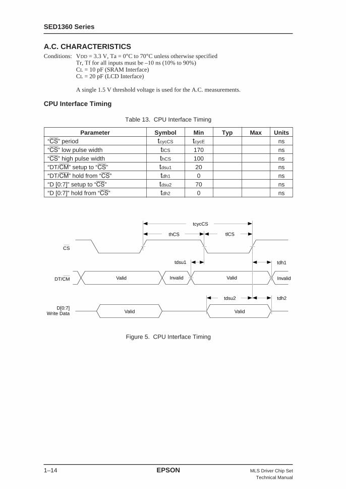
A.C. CHARACTERISTICSConditions: VDD = 3.3 V, Ta = 0°C to 70°C unless otherwise specified
Tr, Tf for all inputs must be –10 ns (10% to 90%)CL = 10 pF (SRAM Interface)CL = 20 pF (LCD Interface)
A single 1.5 V threshold voltage is used for the A.C. measurements.
CPU Interface Timing
Table 13. CPU Interface Timing
Parameter Symbol Min Typ Max Units“CS” period tcycCS tcycE ns“CS” low pulse width tlCS 170 ns“CS” high pulse width thCS 100 ns“DT/CM” setup to “CS” tdsu1 20 ns“DT/CM” hold from “CS” tdh1 0 ns“D [0:7]” setup to “CS” tdsu2 70 ns“D [0:7]” hold from “CS” tdh2 0 ns
Figure 5. CPU Interface Timing
Valid DT/CM
CS
D[0:7]Write Data
Invalid Invalid Valid
Valid Valid
tdsu1 tdh1
tdh2
tcycCS
thCS tlCS
tdsu2

SED1360 Series
MLS Driver Chip Set EPSON 1–15Technical Manual
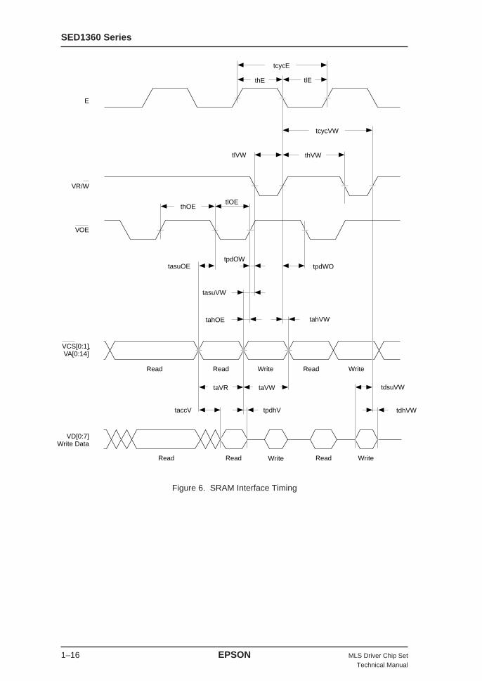
SRAM Interface Timing
Table 14. SRAM Interface Timing
Parameter Symbol Min Typ Max Units“E” period tcycE 333 ns“E” low pulse width tlE 142 ns“E” high pulse width thE 137 ns“VR/W” period tcycVW tcycE ns“VR/W” low pulse width tlVW thE-40 ns“VR/W” high pulse width thVW tlE ns“VA [0:14]”, “VCS [0:1]” setup to “VR/W” tasuVW 0 ns“VA [0:14]”, “VCS [0:1]” hold from tahVW 0 ns“VR/W”“VD [0:7]” setup to “VR/W” tdsuVW tlVW-20 tlVW-10 ns“VD [0:7]” hold from “VR/W” tdhVW 0 nsvalid address period for the Display taVR tlE-15 tlE nsRefreshvalid address period for the CPU data taVW thE-15 thE nswriteSRAM read data access from the valid taccV taVR-25 nsaddressSRAM read data hold time from the tpdhV 0 nsvalid address“VA [0:14]”, “VCS [0:1]” setup to “VOE” tasuOE 0 ns“VOE” hold from “VA [0:14]”, “VCS [0:1]” tahOE 0 ns“VOE” low pulse width tlOE tlE ns“VOE” high pulse width thOE thE ns“VR/W” delay from “VOE” tpdOW 0 ns“VOE” delay from “VR/OW” tpdWO 0 ns
SED1360 Series
1–16 EPSON MLS Driver Chip SetTechnical Manual
Figure 6. SRAM Interface Timing
VCS[0:1]VA[0:14]
VOE
VR/W
E
VD[0:7]Write Data
tcycE
tcycVW
thVW
thOE
taVR tdsuVWtaVW
taccV tpdhV tdhVW
tlOE
tasuOE
Read Read ReadWrite Write
Read Read ReadWrite Write
tpdWO
tasuVW
tahOE tahVW
tlVW
thE tlE
tpdOW
SED1360 Series
MLS Driver Chip Set EPSON 1–17Technical Manual
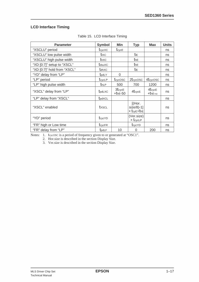
LCD Interface Timing
Table 15. LCD Interface Timing
Parameter Symbol Min Typ Max Units“XSCLU” period tcycXC tcycE ns“XSCLU” low pulse width tlXC tlE ns“XSCLU” high pulse width thXC thE ns“XD [0:7]” setup to “XSCL” tdsuXC thE ns“XD [0:7]” hold from “XSCL” tdhXC tlE ns“YD” delay from “LP” tpdLY 0 ns“LP” period tcycLP tcycOSC 2tcycOSC 4tcycOSC ns“LP” high pulse width thLP 500 700 1200 ns
“XSCL” delay from “LP” tpdLXC3tcycE 4tcycE
4tcycE ns+thE-50 +thE+50
“LP” delay from “XSCL” tpdXCL ns[(Hor.
“XSCL” enabled tXSCL size/8)-1] ns× tcyE+thE
“YD” period tcycYD(Ver.size) ns× tcycLP
“FR” high or Low time tcycFR tcycYD ns“FR” delay from “LP” tpdLF 10 0 200 ns
Notes: 1. tcycOSC is a period of frequency given to or generated at “OSC1”.2. Hor.size is described in the section Display Size.3. Ver.size is described in the section Display Size.
SED1360 Series
1–18 EPSON MLS Driver Chip SetTechnical Manual
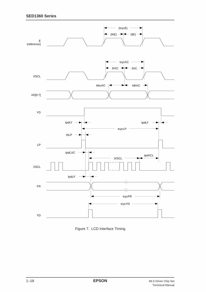
Figure 7. LCD Interface Timing
E(reference)
(tcycE)
(thE) (tlE)
XSCL
XD[0:7]
YD
LP
XSCL
FR
YD
tcycXC
thXC tlXC
tdsuXC tdhXC
tpdLYtpdLY
tcycLP
tcycFR
tcycYD
tpdLXC
tpdLF
tXSCLtpdXCL
thLP

SED1360 Series
MLS Driver Chip Set EPSON 1–19Technical Manual
Oscillation Timing
Table 16. LCD Interface Timing
Figure 8. LCD Interface Timing
Parameter Symbol Min Typ Max Units
“OSC1” period tcycOSC20 41.7 50 µstOSC = 50 kHz fOSC = 24 kHz fOSC = 20 kHz
“OSC1” low width if external tlOSC 0.5tcycOSC µsoscillation is used.“OSC1” high width if external thOSC 0.5tcycOSC µsoscillation is used.
OSC1
tcycOSC
tlOSC thOSC
OPERATION DESCRIPTIONCPU Write Data TransferThe following figure gives a basic timing for SED1360 to receive the CPU Write Data and relationshipbetween CPU Data and pixels on the LCD panel. It is assumed that both CPU Write Start Address andDisplay Refresh Start Address are the same and the 320 × 200 dot LCD is used in the following figure.(1) The rising edge of “CS” is used for SED1360 to latch the CPU data.(2) The CPU Data Write, after the “Display Data Write” command is executed, will be stored in the
SRAM according to the internal CPU Write Address.(3) The first 40 Byte data will be stored in SRAM and displayed continuously on the same line.(4) The data will be displayed at the most left position on the next line on the panel every 40 Byte data.
SED1360 Series
1–20 EPSON MLS Driver Chip SetTechnical Manual
Figure 9. CPU Write Data Transfer
CS
DT/CM
D[0:7]
D[0:7]
XD[0:7]
200 Lines
d0
D7 D6 D5 D4 D3 D2 D1 D0
d1 d2 d3com.
D7 D6 D5 D4 D3 D2 D1 D0
d0 d1 d2 d38 d39
d7960 d7961 d7962 d7998 d7999
320 Dots
Enables CPUCommand Write
Enables CPUData Write
Bit Order on the LCD Panel
B & W LCD Panel

SED1360 Series
MLS Driver Chip Set EPSON 1–21Technical Manual
Display Data Transfer ModesDisplay Data Auto Transfer Mode
The following figure gives a basic operation mode which SED1360 switches automatically. The figureassumes that the chip is configured in Display Data Auto Transfer Mode.(1) If CPU Display Data Write Access occurs, then the next Frame period will be Active Mode. That is
the Active Mode is initiated by the CPU Display Data Write Access, if the chip is configured inDisplay Data Auto Transfer Mode.
(2) If no CPU Display Data Write Access occurs in one Frame period, then the next Frame period willbe Doze Mode.
(3) SED1360 switches the whole LCD Display Subsystem between Doze Mode and Active Mode.(4) In the Active Mode, SED1360 reads the data from the SRAM, enables “XSCLU” in order to transfer
the data stored in the SRAM to the LCD Module, then the RAM integrated Segment Drivers wake upfrom the power save mode.
(5) In the Doze Mode, SED1360 stops reading the data from the SRAM, disables “XSCLU” in order forthe RAM integrated Segment Drivers to enter into the Power Save Mode.

SED1360 Series
1–22 EPSON MLS Driver Chip SetTechnical Manual
Figure 10. Display Data Auto Transfer Mode
CS
Internal FrameStart Signal
Internal CPUWrite status
InternalOperation
Mode
E
Active DozeDoze DozeActive ActiveDoze
VR/W
VCS[0:1]
XSCLU
XD[0:7]
YD
2 Frame Period/Max.

SED1360 Series
MLS Driver Chip Set EPSON 1–23Technical Manual
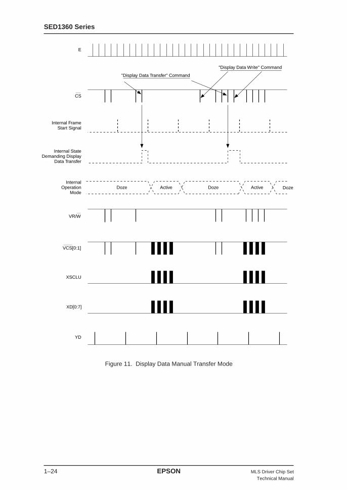
Display Data Manual Transfer Mode
The following figure gives another basic operation mode which SED1360 controls Active Mode with the“Display Data Transfer” command. The figure assumes that the chip is configured in Display Data ManualTransfer Mode.(1) If the “Display Data Transfer” command is set to the chip, then the next Frame period will be Active
Mode. That is the Active Mode is initiated by the Display Data Transfer” command, if the chip isconfigured in Display Data Manual Transfer Mode.
(2) Once one Frame of display data, which are in the SRAM, are transferred to the LCD Module, the chipswitches to Doze Mode and it keeps the Doze Mode until next “Display Data Transfer” command isexecuted. But if the next “Display Data Transfer” command is set without having any othercommands between these two “Display Data Transfer” commands, the next “Display Data Transfer”command is ignored. That is in this case the next “Display Data Transfer” command does not set thechip in the Active Mode.
(3) SED1360 switches the whole LCD Display Subsystem between Doze Mode and Active Mode.(4) In the Active Mode, SED1360 reads the data from the SRAM, enables “XSCLU” in order to transfer
the data stored in the SRAM to the LCD Module, then the RAM integrated Segment Drivers wake upfrom the power save mode.
(5) In the Doze Mode, SED1360 stops reading the data from the SRAM, disables “XSCLU” in order forthe RAM integrated Segment Drivers to enter into the Power Save Mode.
SED1360 Series
1–24 EPSON MLS Driver Chip SetTechnical Manual
Figure 11. Display Data Manual Transfer Mode
CS
Internal FrameStart Signal
Internal StateDemanding Display
Data Transfer
InternalOperation
Mode
E
Active DozeDozeActiveDoze
VR/W
VCS[0:1]
XSCLU
XD[0:7]
YD
"Display Data Transfer" Command
"Display Data Write" Command
SED1360 Series
MLS Driver Chip Set EPSON 1–25Technical Manual
Sleep ModeSED1360 can enter into the Sleep Mode by setting the “SLEEP” signal low. This mode is prepared to shutthe whole LCD Display Subsystem off with keeping the data in the SRAM. In the Sleep Mode, the chipwill be in the following state.(1) The internal oscillation is displayed.(2) VA [0:14] output low, VCS [0:1] output high, VD [0:7] will be high impedance (pins are pulled high
by the integrated pull-up resisters).(3) “FR”, “YD”, “LP”, “XSCLU”, “XD [0:7]” and “ DOFF” output low. VOE, VR/W output high.(4) “D [0:7]”, “E” “ CS”, “DT/ CM” and “RESET” are internally masked but they also should be kept in
invalid state.
OSCILLATION DESCRIPTIONSED1360’s Hardware is optimized to display 320 × 200 LCD panel driven by RAM integrated SegmentDrivers as a default chip configuraiton. This section describes how to determine the frequency which isinput to OSC1 and how to generate the frequency by using the internal oscillation function.
OSC1 Frequency DeterminationConditions: 320 × 200 single scan LCD panel assumes 60 Hz as an LCD frame frequency(1) “LP” period is obtained by the following calculation.
60 × 200 = 12 kHz(2) If an external oscillator is used, the OSC1 frequency can be the same as “LP”. Then 12 kHz is the
required frequency for OSC1.(3) If an internal oscillator is used, the oscillation frequency has to be doubled to be 24 kHz. The internal
oscillation might be unstable below 24 kHz. So if the required frequency is below 20 kHz, it isrecommended to generate doubled frequency. There is a register which divides the internal oscillationfrequency by two, four or eight.
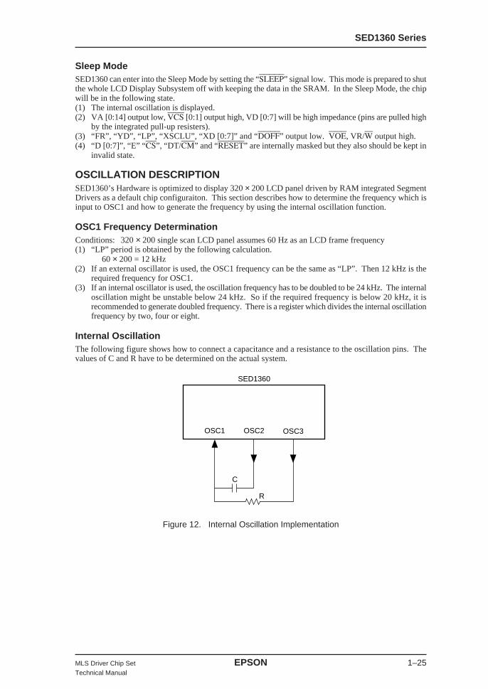
Internal OscillationThe following figure shows how to connect a capacitance and a resistance to the oscillation pins. Thevalues of C and R have to be determined on the actual system.
Figure 12. Internal Oscillation Implementation
OSC1
C
OSC2
SED1360
OSC3
R

SED1360 Series
1–26 EPSON MLS Driver Chip SetTechnical Manual
COMMAND DESCRIPTIONSED1360 has several commands which can manipulate the data transfer procedure between CPU, SRAM,LCD Module and SED1360.
Display Size
command; DT/CM = 0D7 D6 D5 D4 D3 D2 D1 D00 0 0 0 0 0 0 1 01H
data; DT/CM = 10 0 HC5 HC4 HC3 HC2 HC1 HC0 data1
VC7 VC6 VC5 VC4 VC3 VC2 VC1 VC0 data2
(1) This command sets the size of the display.(2) This command requires two bytes of data which follow this command.(3) The first data defines a horizontal size of the display in byte unit, and the second data defines a vertical
size of the display in line unit.(4) The horizontal size is set 320 dots and the vertical size is set 200 lines when the “RESET” signal is
set low.
Table 17. Horizontal Size Table 18. Vertical Size
Hor. size HC [5:0]8 00h16 01h24 02h
240 1Dh
320 27h
512 3Fh
Ver. size VC [7:0]1 00h2 01h3 02h
200 C7h
240 Efh
256 Ffh
Display Data Auto Transfer Mode
(1) This command configures the chip in the Display Data Auto Transfer Mode. Detailed functionalexplanation is described in “Display Data Auto Transfer Mode”.
command; DT/CM = 0D7 D6 D5 D4 D3 D2 D1 D00 0 0 0 0 0 1 0 02H
SED1360 Series
MLS Driver Chip Set EPSON 1–27Technical Manual
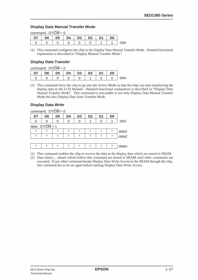
Display Data Manual Transfer Mode
(1) This command configures the chip in the Display Data Manual Transfer Mode. Detailed functionalexplanation is described in “Display Manual Transfer Mode”.
Display Data Transfer
command; DT/CM = 0D7 D6 D5 D4 D3 D2 D1 D00 0 0 0 0 0 1 1 03H
(1) This command force the chip to go into the Active Mode so that the chip can start transferring thedisplay data to the LCD Module. Detailed functional explanation is described in “Display DataManual Transfer Mode”. This command is executable in not only Display Data Manual TransferMode but also Display Data Auto Transfer Mode.
Display Data Write
command; DT/CM = 0D7 D6 D5 D4 D3 D2 D1 D00 0 0 0 0 1 0 0 04H
(1) This command enables the chip to receive the data as the display data which are stored in SRAM.(2) Data (data1,…datan) which follow this command are stored in SRAM until other commands are
executed. If any other command breaks Display Data Write Access to the SRAM through the chip,this command has to be set again before starting Display Data Write Access.
command; DT/CM = 0D7 D6 D5 D4 D3 D2 D1 D00 0 0 0 0 1 0 1 05H
data; DT/CM = 1* * * * * * * * data1* * * * * * * * data2
* * * * * * * * datan
SED1360 Series
1–28 EPSON MLS Driver Chip SetTechnical Manual
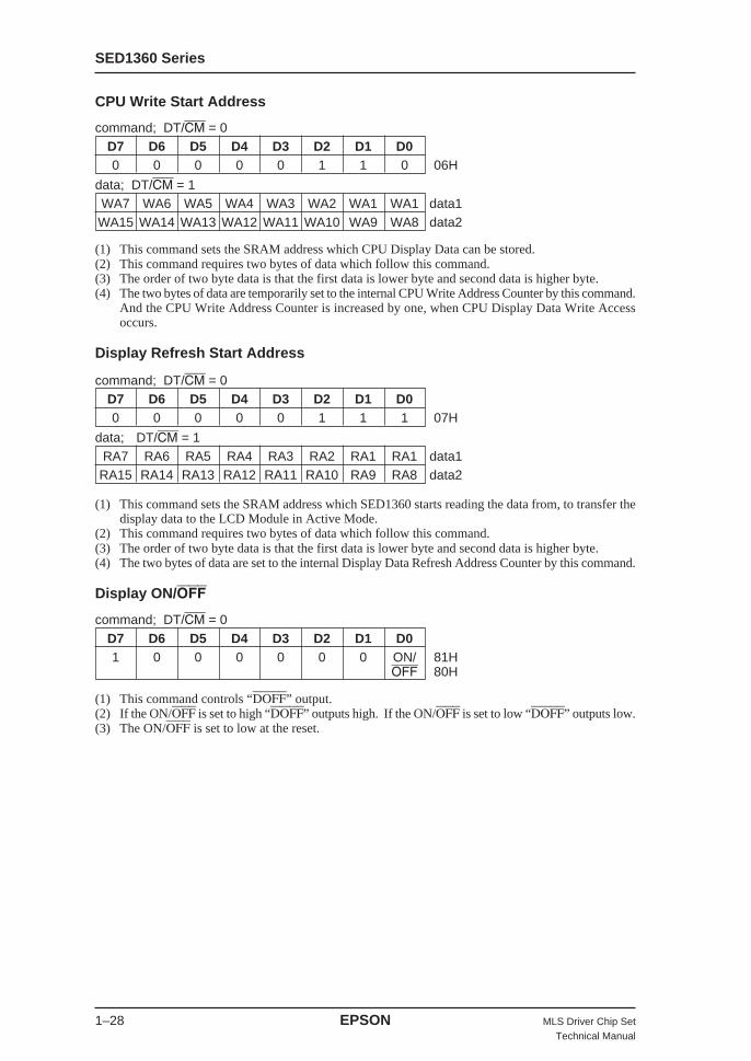
CPU Write Start Address
(1) This command sets the SRAM address which CPU Display Data can be stored.(2) This command requires two bytes of data which follow this command.(3) The order of two byte data is that the first data is lower byte and second data is higher byte.(4) The two bytes of data are temporarily set to the internal CPU Write Address Counter by this command.
And the CPU Write Address Counter is increased by one, when CPU Display Data Write Accessoccurs.
Display Refresh Start Address
command; DT/CM = 0D7 D6 D5 D4 D3 D2 D1 D00 0 0 0 0 1 1 0 06H
data; DT/CM = 1WA7 WA6 WA5 WA4 WA3 WA2 WA1 WA1 data1WA15 WA14 WA13 WA12 WA11 WA10 WA9 WA8 data2
command; DT/CM = 0D7 D6 D5 D4 D3 D2 D1 D00 0 0 0 0 1 1 1 07H
data; DT/CM = 1RA7 RA6 RA5 RA4 RA3 RA2 RA1 RA1 data1
RA15 RA14 RA13 RA12 RA11 RA10 RA9 RA8 data2
(1) This command sets the SRAM address which SED1360 starts reading the data from, to transfer thedisplay data to the LCD Module in Active Mode.
(2) This command requires two bytes of data which follow this command.(3) The order of two byte data is that the first data is lower byte and second data is higher byte.(4) The two bytes of data are set to the internal Display Data Refresh Address Counter by this command.
Display ON/ OFF
command; DT/CM = 0D7 D6 D5 D4 D3 D2 D1 D01 0 0 0 0 0 0 ON/ 81H
OFF 80H
(1) This command controls “DOFF” output.(2) If the ON/OFF is set to high “DOFF” outputs high. If the ON/OFF is set to low “DOFF” outputs low.(3) The ON/OFF is set to low at the reset.
SED1360 Series
MLS Driver Chip Set EPSON 1–29Technical Manual
LP Configuration
command; DT/CM = 0D7 D6 D5 D4 D3 D2 D1 D00 0 0 0 1 0 0 0 08H
(1) This command selects “LP” period.(2) FS1,0 select the period of the signal “LP”. The following table shows how to select the required
frequency for the signal “LP”.(3) FS [1,0] = [0,0] is set when the “RESET” signal is set low.
data; DT/CM = 10 0 0 0 0 0 FS1 FS0 data1
Table 19. LP Frequency
FS1 FS0 LP frequency0 0 fOSC
0 1 fOSC/21 0 fOSC/41 1 fOSC/8
ERRORTAThis version has one error. About CPU Write Start Address, Values which CPU wrote is increased by one.So, you should set values which is decreased by one.
NOTICENo parts of this material may be reproduced or duplicated in any form or by any means without the writtenpermission of Seiko Epspn. Seiko Epson reserves the right to make changes to this material without notice.Seiko Epson does not assume any liability of any kind aristing out of any inaccuracies contained in thismaterial or due to its application or use in any product or circuit and, further, there is no representation thatthis material is applicable to products requiring high level reliability, such as, medical products. Moreover,no license to any intellectual property rights is granted by implication or otherwise, and there is norepresentation or warranty what anything made in accordance with this material will be free from anypatent or copyright infringement of a third party. This material or portions there of may contain technologyor the subject relating to strategic products under the control of the Foreign Exchange and Foreign TradeControl Law of Japan and may require an export license from the Ministry of International Trade andIndustry or other approval from another government agency.Pay attention to the following point when using a semiconductor device. A semiconductor device will bedeteriorated in its characteristic when it is exposed to light. For this reason, this IC might malfunction insome cases when exposed to the light. To avoid causing such malfunction, steps be taken to shield the lightin its packaging or enclosure to prevent the surface, rear and side of this IC from being exposed to the light.

SED1580
SED1580
MLS Driver Chip Set EPSON iTechnical Manual
Contents
INTRODUCTION........................................................................................................................... 2-1
FEATURES ................................................................................................................................... 2-1
BLOCK DIAGRAM ........................................................................................................................ 2-2
PIN CONFIGURATION ................................................................................................................. 2-3
ELECTRICAL CHARACTERISTICS ........................................................................................... 2-15
POWER SOURCE ...................................................................................................................... 2-19
EXAMPLE OF EXTERNAL CONNECTIONS.............................................................................. 2-20

SED1580
MLS Driver Chip Set EPSON 2–1Technical Manual
OVERVIEWDescriptionThe SED1580 is a 160-output, 5-level segment (column) driver for MLS (Multi-Line Selection) driving,able to drive with both high contrast and high speed. It is used in conjunction with the SED1751. Whenpaired with the SED1751 it can be connected to the SED1360 LCD controller.Because the SED1580 stores display data in its internal display RAM and generates LC drive signals,display data transmission from the controller can be suspended except for when there are changes to thedisplay, thereby enabling an ultra low power display system.The SED1580 uses a slim package, facilitating the construction of thinner LCD panels, and the low-voltageoperation of its logic power source makes it appropriate to a wide range of applications.
FEATURES• Number of simultaneous line selects: 4 Lines• Drive duty ratio (MAX) 1/240 duty• LCD driver outputs 160 outputs• Internal display RAM 160 × 240 bit• Extremely low consumption current• Power Source Voltages Logic System: 3.0 to 3.6V (Max)
LCD System: 6.0 to 7.2V (Max)• High speed, low power data transmission possible through the 4-bit/8-bit switchable bus enable chain
method• Non-biased display off function• Output shift direction pin select supported• Slim chip shape• Shipment status:
In CHIP form .................SED1580D0B
In TCP form ................... SED1580T0A
• This product is not designed for resistance to light or radiation
SED1580
2–2 EPSON MLS Driver Chip SetTechnical Manual
BLOCK DIAGRAMBlock Diagram
LCD Driver
Level Shifter
MLS Decoder
X1 X160
V3V2Vc
-V2-V3
VDDVSS
FRDOFF
YDCA
LSEL
LPXSCL
F2SF1SF2OF1O
D0~7
SHL
EIO1EIO2
Data Register
Enable Controller
Frame Memory
Bi-DirectionalShift Register
DataController
ControlCircuit
Column AddressGenerator Circuit

SED1580
MLS Driver Chip Set EPSON 2–3Technical Manual
PIN CONFIGURATIONPad Layout
Chip size 12.89 mm × 2.77 mmBump pitch: 103 microns (Min.)Chip thickness: 625 microns ± 15 µm
195
1
196
215
76
55
75
56
X
Y
Pad numberX Y
56 to 215 67 63
1, 7 to 16, 18 to 36, 38 to 49, 55 74 74
2 to 6, 17, 37, 50 to 54 110 74
22 110 75
ItemsSpecifications
MIN TYP MAX
Bump size specifications –4 µm Bump size +4 µm
Bump height specifications –5.5 µm 22.5 µm +5.5 µm
Bump strength 30g
Bump size (Unit: µm)
Bump specifications (reference values)

SED1580
2–4 EPSON MLS Driver Chip SetTechnical Manual
Pin CoordinatesSED1580 Bump Center Coordinates
63 X8 6303 –26564 X9 –15965 X10 –5366 X11 5367 X12 15968 X13 26569 X14 37270 X15 47871 X16 58472 X17 69073 X18 79774 X19 90375 X20 100976 X21 6098 124677 X22 599578 X23 589379 X24 579080 X25 568881 X26 558582 X27 548383 X28 538084 X29 527885 X30 517586 X31 507387 X32 497088 X33 486889 X34 476590 X35 466391 X36 456092 X37 445893 X38 435594 X39 425395 X40 415096 X41 404897 X42 394598 X43 384399 X44 3740
100 X45 3637101 X46 3535102 X47 3432103 X48 3330104 X49 3227105 X50 3125106 X51 3022107 X52 2920108 X53 2817109 X54 2715110 X55 2612111 X56 2510112 X57 2407113 X58 2305114 X59 2202115 X60 2100116 X61 1997117 X62 1895118 X63 1792119 X64 1690120 X65 1587121 X66 1485122 X67 1382123 X68 1280124 X69 1177
Pin Name X Y
125 X70 1075 1246126 X71 972127 X72 870128 X73 767129 X74 665130 X75 562131 X76 460132 X77 357133 X78 255134 X79 152135 X80 50136 X81 –52137 X82 –154138 X83 –257139 X84 –359140 X85 –462141 X86 –564142 X87 –567143 X88 –769144 X89 –872145 X90 –974146 X91 –1077147 X92 –1179148 X93 –1282149 X94 –1385150 X95 –1487151 X96 –1590152 X97 –1692153 X98 –1795154 X99 –1897155 X100 –2000156 X101 –2102157 X102 –2205158 X103 –2307159 X104 –2410160 X105 –2512161 X106 –2615162 X107 –2717163 X108 –2820164 X109 –2922165 X110 –3025166 X111 –3127167 X112 –3230168 X113 –3332169 X114 –3435170 X115 –3537171 X116 –3640172 X117 –3742173 X118 –3845174 X119 –3947175 X120 –4050176 X121 –4152177 X122 –4255178 X123 –4357179 X124 –4460180 X125 –4562181 X126 –4655182 X127 –4767183 X128 –4870184 X129 –4972185 X130 –5075186 X131 –5177
Pin Name X YPin Name X Y
1 EIO2 –5378 –12402 –V3 –52223 –V2 –50444 VC –48665 V2 –46886 V3 –45107 NC –43228 NC –41449 NC –396610 NC –378911 NC –361112 F1O –344913 F2O –291514 NC –226615 SHL –208616 TEST –190617 VSS –172618 BSEL –154619 LSEL –136620 FR –118621 YD –100622 NC –82623 CA –54624 LP –46625 XSCL –28626 D0 16327 D1 34328 D2 52329 D3 70330 D4 88331 D5 106332 D6 124333 D7 142334 F2S 160335 F1S 178336 DOFF 196337 VDD 214338 NC 238739 NC 256440 NC 274241 NC 292042 NC 309843 NC 327544 NC 345345 NC 363146 NC 380947 NC 398648 NC 416449 NC 434250 V3 472251 V2 490052 VC 507753 –V2 525554 –V3 543355 EIO1 562956 X1 6303 –100957 X2 –90358 X3 –79759 X4 –69060 X5 –58461 X6 –47862 X7 –371
Units: µm
SED1580
MLS Driver Chip Set EPSON 2–5Technical Manual
Pin Name X YPin Name X Y
197 X142 –6303 903198 X143 797199 X144 690200 X145 584201 X146 478202 X147 372203 X148 265204 X149 159205 X150 53206 X151 –53
207 X152 –6303 –159208 X153 –265209 X154 –371210 X155 –478211 X156 –584212 X157 –690213 X158 –797214 X159 –903215 X160 –1009
Pin Name X Y
187 X132 –5280 1246188 X133 –5382189 X134 –5485190 X135 –5587191 X136 –5690192 X137 –5792193 X138 –5895194 X139 –5997195 X140 –6100196 X141 –6303 1009
Units: µm
Pin FunctionsPin Functions Table
Pin Name I/O Function # ofPins
X1 to O Segment (column) output to drive the LC. 160X160 Output transition occurs on falling edge of LP.
BSEL I Display data input bit number select input. “L”: 4 bit input. 1“H”: 8 bit input.
LSEL I 1/2 H operation select input. “L”: Normal operation. 1“H”: 1/2 H operation.
D0 to D7 I Display data input. When 4 bit input is used, D0 to D3 is used, 8and D4 to D7 can be left NC.
XSCL I Display data shift clock input. Display data (D0 to D7) is read 1sequentially into the data register on the falling edge.Display data latch clock input* Accepts into the LCD driver the control signal from the LC driver selected by the MLS decoder, doing so at the fallingedge, and outputs the LC driver output.
LP I * Writes the contents of the data registers to the frame memory 1 4 LP at a time for the specified column address.* Resets the enable control circuit.* When 1/2 operation is selected, inputs the LP with twice the normal frequency.Enable I/O* Is set to input or output depending on the SHL input level.
EIO1 * When output, the LP input is reset (in an “H” state), and when 1EIO2 I/O the 160 bit of display data has been read in, the signal 1 automatically falls to L.
* When connected in cascade, is connected to the next stage EIO input.
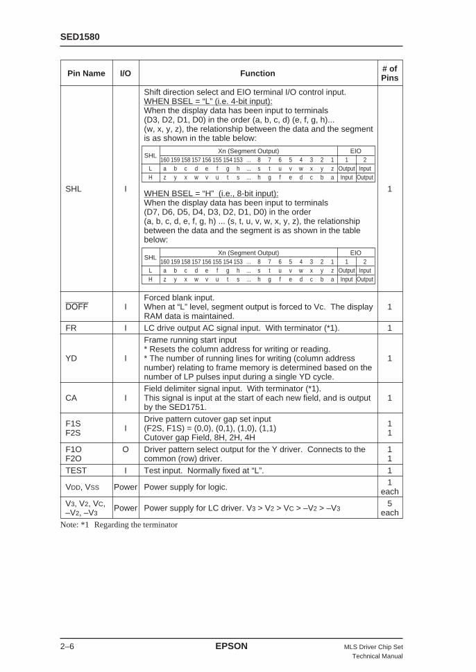
SED1580
2–6 EPSON MLS Driver Chip SetTechnical Manual
Pin Name I/O Function # ofPins
Shift direction select and EIO terminal I/O control input.WHEN BSEL = “L” (i.e. 4-bit input):When the display data has been input to terminals(D3, D2, D1, D0) in the order (a, b, c, d) (e, f, g, h)...(w, x, y, z), the relationship between the data and the segmentis as shown in the table below:
SHL I 1WHEN BSEL = “H” (i.e., 8-bit input):When the display data has been input to terminals(D7, D6, D5, D4, D3, D2, D1, D0) in the order(a, b, c, d, e, f, g, h) ... (s, t, u, v, w, x, y, z), the relationshipbetween the data and the segment is as shown in the tablebelow:
Forced blank input.DOFF I When at “L” level, segment output is forced to Vc. The display 1
RAM data is maintained.FR I LC drive output AC signal input. With terminator (*1). 1
Frame running start input* Resets the column address for writing or reading.
YD I * The number of running lines for writing (column address 1number) relating to frame memory is determined based on thenumber of LP pulses input during a single YD cycle.Field delimiter signal input. With terminator (*1).
CA I This signal is input at the start of each new field, and is output 1by the SED1751.
F1S Drive pattern cutover gap set input 1F2S I (F2S, F1S) = (0,0), (0,1), (1,0), (1,1) 1Cutover gap Field, 8H, 2H, 4HF1O O Driver pattern select output for the Y driver. Connects to the 1F2O common (row) driver. 1TEST I Test input. Normally fixed at “L”. 1
VDD, VSS Power Power supply for logic. 1each
V3, V2, VC, Power Power supply for LC driver. V3 > V2 > VC > –V2 > –V35
–V2, –V3 eachNote: *1 Regarding the terminator
SHLXn (Segment Output) EIO
160 159 158 157 156 155 154 153 ... 8 7 6 5 4 3 2 1 1 2L a b c d e f g h ... s t u v w x y z Output InputH z y x w v u t s ... h g f e d c b a Input Output
SHLXn (Segment Output) EIO
160 159 158 157 156 155 154 153 ... 8 7 6 5 4 3 2 1 1 2L a b c d e f g h ... s t u v w x y z Output InputH z y x w v u t s ... h g f e d c b a Input Output
SED1580
MLS Driver Chip Set EPSON 2–7Technical Manual
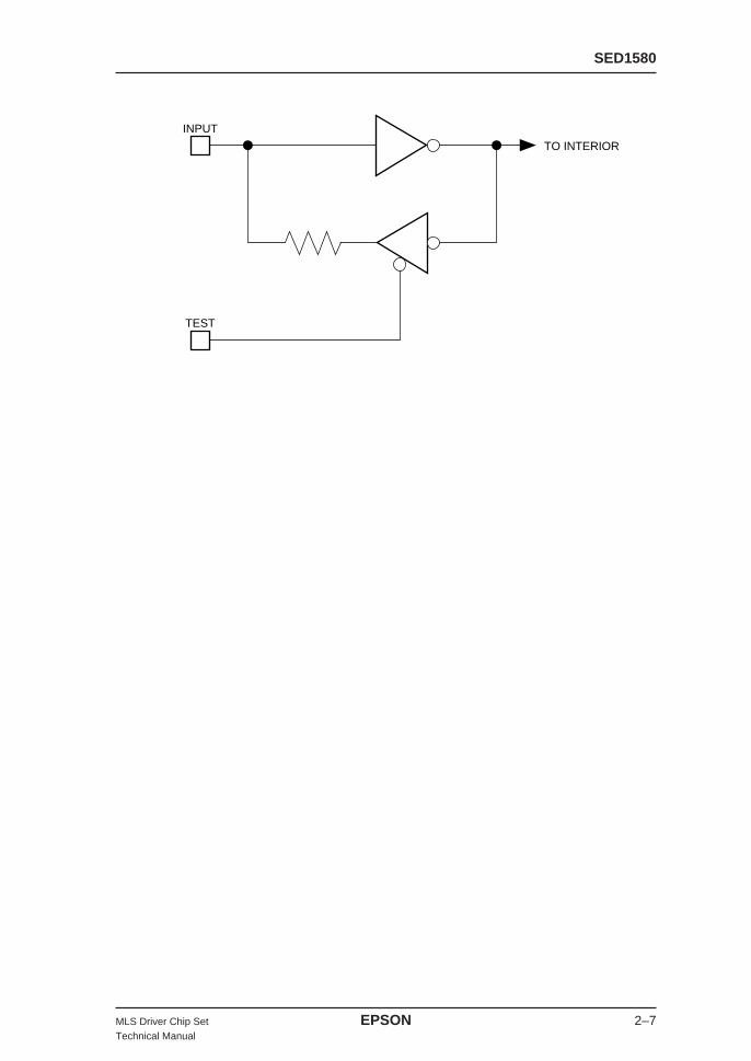
TEST
INPUT
TO INTERIOR

SED1580
2–8 EPSON MLS Driver Chip SetTechnical Manual
FUNCTIONSThe Functional BlocksEnable ControlWhen the enable signal is in a disable state (EIO = “H”), the internal clock signal and data bus are fixedat “L”, placing the chip in power save mode.When multiple segment drivers are used, the EIO terminals of the various drivers are cascade connectedand the EIO terminal of the first driver is connected to “VSS”.The enable control circuit automatically senses when 160 bits worth of data have been received, andautomatically sends the enable signal, thus eliminating the need for a control signal from the control LSI.
Bi-directional Shift RegisterThis sends the control signal for writing the display data D0 – D7 to the data register. The order in whichthe display data is latched into the data register by the SHL input is returned (SIC? Reversed?).
Data RegisterThis is a 160 dot register which controls writing to the display RAM. It has 4 lines. At each falling edgeof the LP signal it accepts display data from one line, and writes to the frame memory after it has stored4 lines of data.
Frame MemoryThis is static RAM (with peripheral circuits) that stores LC display data. It has a capacity of 160 segmentsby 240 lines.
MLS DecoderThis outputs the drive control signals necessary for the 4 MLS driving. The control signal is set by fieldinformation provided by the four lines of display data, FR, DOFF, and the control circuit.
LCD DriverThe LCD driver outputs the LC drive voltage. The driver voltage is selected by the control signal fromthe 5 levels V3, V2, VC, –V2 and –V3, determined by the MLS decoder.
Column Address Generating CircuitWhen writing to or reading from frame memory, this outputs the column address corresponding to thelocation of the RAM in frame memory.
Level ShifterThis is a level interface circuit used to convert signal levels when signals are propagated from low-voltageparts to high-voltage parts.
Data ControlThis accepts display data input when enabled, and sends it to the data register.
Control CircuitThis determines the self refresh rate, enables the data register to write to the display RAM, controls theoutput of the column address generator, and performs field control on the MLS decoder.
The Self Refresh FunctionSetting the Self Refresh Mode“Self refresh mode” refers to a situation where the transmission of display data from the display controllerto the SED1580 is suspended when the content of the display does not change, and where the SED1580automatically senses this and enters a power down display mode.To place the SED1580 in the self refresh mode maintain the shift clock XSCL at the “L” level during fourhorizontal display periods (4x the LP signal period) after the completion of the input of the display dataof an n + 3 line.When the XSCL is suspended, the power is reduced, so display data inputs D0 – D7 are suspended, as istransmission from the display controller, being set to “H” or “L”. At this time the display controller mustsend LP, YD, or FR signals periodically to the SED1580 as it does when data is being sent. The SED1580receives these signals, periodically reads display data from its internal RAM, and refreshes the display.The display off function is operational even when in the self refresh mode.
Getting Out of the Self Refresh ModeIn order to get out of the self refresh mode, the display controller inputs the shift clock XSCL to theSED1580 for four or more horizontal display periods with the timing of the data transmission from thefalling edge of the LP signal at the time of an n + 3 line. With the falling edge of the LP signal after thefourth horizontal period after getting out of this mode, the display data transmitted during the fourhorizontal display intervals is written to frame memory.When SED1580s are cascade connected, if the number of XSCL clocks input does not correspond to thecascade connections, then not all of the SED1580s will be released from self refresh mode.

SED1580
MLS Driver Chip Set EPSON 2–9Technical Manual
Note: When the number of lines is 240:
n lines 1, 5, 9, ...233, 237 (1 + multiples of 4)n + 1 lines 2, 6, 10,...234, 238 (2 + multiples of 4)n + 2 lines 3, 7, 11,...235, 239 (3 + multiples of 4)n + 3 lines 4, 8, 12,...236, 240 (Multiples of 4)
First field In the order (1,1) → (1,0) → (0,1) → (0,0) → (1,1) → (1,0) → (0,1) → (0,0)Second field In the order (1,0) → (0,1) → (0,0) → (1,1) → (1,0) → (0,1) → (0,0) → (1,1)Third field In the order (0,1) → (0,0) → (1,1) → (1,0) → (0,1) → (0,0) → (1,1) → (1,0)Fourth field In the order (0,0) → (1,1) → (1,0) → (0,1) → (0,0) → (1,1) → (1,0) → (0,1)
FR L HF1O 1 0 1 0 1 0 1 0F2O 1 1 0 0 1 1 0 0
n line V1 V1 –V1 V1 –V1 –V1 V1 –V1n + 1 line –V1 V1 V1 V1 V1 –V1 –V1 –V1n + 2 line V1 –V1 V1 V1 –V1 V1 –V1 –V1n + 3 line V1 V1 V1 –V1 –V1 –V1 –V1 V1
Note: Voltage relationships: V1 > VC > –V1 (VC is the middle voltage level)
The transitions in (F2O, F1O) within each field when the drive pattern changes:
This is determined by the values of the inputs (F2S, F1S) during the changeover interval. The relationshipbetween F2S and F1S and the changeover interval is as follows:
When the changeover interval is selected for each field, the value stored in the field is the first value shownin the shown in the (F2O, F1O) change table above (the value on the left).
The Relationship Between Drive Output Voltages and Display DataF20, F10, and the common drive voltage have the following relationships:
F2S F1S Changeover Interval0 0 Field0 1 8-line interval1 0 2-line interval1 1 4-line interval
SED1580
2–10 EPSON MLS Driver Chip SetTechnical Manual
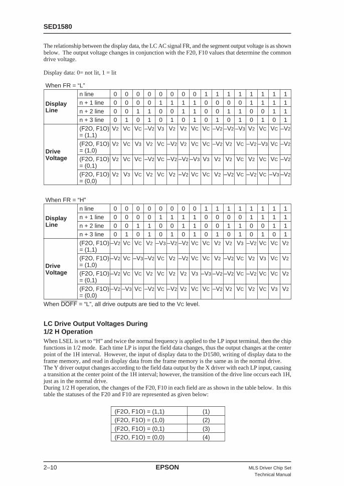
The relationship between the display data, the LC AC signal FR, and the segment output voltage is as shownbelow. The output voltage changes in conjunction with the F20, F10 values that determine the commondrive voltage.
Display data: 0= not lit, 1 = lit
When FR = “L”n line 0 0 0 0 0 0 0 0 1 1 1 1 1 1 1 1
Display n + 1 line 0 0 0 0 1 1 1 1 0 0 0 0 1 1 1 1Line n + 2 line 0 0 1 1 0 0 1 1 0 0 1 1 0 0 1 1
n + 3 line 0 1 0 1 0 1 0 1 0 1 0 1 0 1 0 1(F2O, F1O) V2 VC VC –V2 V3 V2 V2 VC VC –V2 –V2 –V3 V2 VC VC –V2= (1,1)(F2O, F1O) V2 VC V3 V2 VC –V2 V2 VC VC –V2 V2 VC –V2 –V3 VC –V2
Drive = (1,0)Voltage (F2O, F1O) V2 VC VC –V2 VC –V2 –V2 –V3 V3 V2 V2 VC V2 VC VC –V2
= (0,1)(F2O, F1O) V2 V3 VC V2 VC V2 –V2 VC VC V2 –V2 VC –V2 VC –V3 –V2= (0,0)
When FR = “H”n line 0 0 0 0 0 0 0 0 1 1 1 1 1 1 1 1
Display n + 1 line 0 0 0 0 1 1 1 1 0 0 0 0 1 1 1 1Line n + 2 line 0 0 1 1 0 0 1 1 0 0 1 1 0 0 1 1
n + 3 line 0 1 0 1 0 1 0 1 0 1 0 1 0 1 0 1(F2O, F1O) –V2 VC VC V2 –V3 –V2 –V2 VC VC V2 V2 V3 –V2 VC VC V2= (1,1)(F2O, F1O) –V2 VC –V3 –V2 VC V2 –V2 VC VC V2 –V2 VC V2 V3 VC V2
Drive = (1,0)Voltage (F2O, F1O) –V2 VC VC V2 VC V2 V2 V3 –V3 –V2 –V2 VC –V2 VC VC V2
= (0,1)(F2O, F1O) –V2 –V3 VC –V2 VC –V2 V2 VC VC –V2 V2 VC V2 VC V3 V2= (0,0)
When DOFF = “L”, all drive outputs are tied to the VC level.
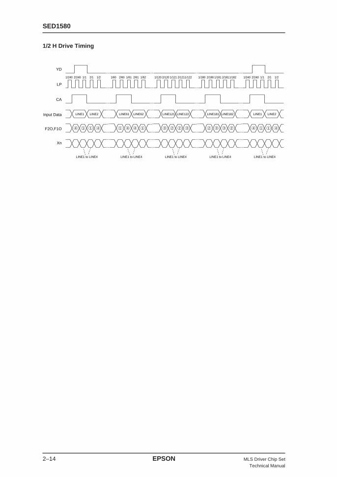
LC Drive Output Voltages During1/2 H OperationWhen LSEL is set to “H” and twice the normal frequency is applied to the LP input terminal, then the chipfunctions in 1/2 mode. Each time LP is input the field data changes, thus the output changes at the centerpoint of the 1H interval. However, the input of display data to the D1580, writing of display data to theframe memory, and read in display data from the frame memory is the same as in the normal drive.The Y driver output changes according to the field data output by the X driver with each LP input, causinga transition at the center point of the 1H interval; however, the transition of the drive line occurs each 1H,just as in the normal drive.During 1/2 H operation, the changes of the F20, F10 in each field are as shown in the table below. In thistable the statuses of the F20 and F10 are represented as given below:
(F2O, F1O) = (1,1) (1)(F2O, F1O) = (1,0) (2)(F2O, F1O) = (0,1) (3)(F2O, F1O) = (0,0) (4)
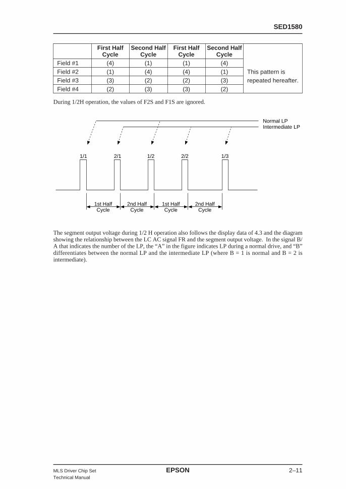
SED1580
MLS Driver Chip Set EPSON 2–11Technical Manual
First Half Second Half First Half Second HalfCycle Cycle Cycle Cycle
Field #1 (4) (1) (1) (4)Field #2 (1) (4) (4) (1) This pattern isField #3 (3) (2) (2) (3) repeated hereafter.Field #4 (2) (3) (3) (2)
During 1/2H operation, the values of F2S and F1S are ignored.
The segment output voltage during 1/2 H operation also follows the display data of 4.3 and the diagramshowing the relationship between the LC AC signal FR and the segment output voltage. In the signal B/A that indicates the number of the LP, the “A” in the figure indicates LP during a normal drive, and “B”differentiates between the normal LP and the intermediate LP (where B = 1 is normal and B = 2 isintermediate).
1/1 2/1 1/2 2/2 1/3
Normal LPIntermediate LP
1st HalfCycle
2nd HalfCycle
1st HalfCycle
2nd HalfCycle

SED1580
2–12 EPSON MLS Driver Chip SetTechnical Manual
Timing diagram (assuming 1/240 duty)
(This diagram provided only as a reference.)
Normal Drive Timing
240
YD
LP
CA
FIELD(Output)
FR
Xn
LP
XSCL
D0 to 7
EIO_1
EIO_2
EIO_N
FIELD #1 FIELD #2 FIELD #3 FIELD #4
1 2
20 1 2 2019 1 2 2019 1 2 2019 1
60 61 62 120 121 122 180 181 182 240 1 2
_1 to _n Indicate Driver Cascade Numbers
3

SED1580
MLS Driver Chip Set EPSON 2–13Technical Manual
F2O, F1O Change Timing
CA
LP
(F2S=0,F1S=0)
(F2S=0,F1S=1)
(F2S=1,F1S=0)
(F2S=1,F1S=1)
YD
LP
XSCL
Input Data
Nn
Self Refresh
Setting and Releasing Self Refresh
SED1580
2–14 EPSON MLS Driver Chip SetTechnical Manual
1/2 H Drive Timing
YD
LP
CA
Input Data
F2O,F1O
Xn
LINE1 LINE2
1/240 2/240 1/1 2/1 1/2
4 1 1
LINE1 to LINE4
4
LINE61 LINE62
1/60 2/60 1/61 2/61 1/62
1 4 4
LINE1 to LINE4
1
LINE121 LINE122
1/120 2/120 1/121 2/1211/122
3 2 2
LINE1 to LINE4
3
LINE181 LINE182
1/180 2/180 1/181 2/1811/182
2 3 3
LINE1 to LINE4
2
LINE1 LINE2
1/240 2/240 1/1 2/1 1/2
4 1 1
LINE1 to LINE4
4
SED1580
MLS Driver Chip Set EPSON 2–15Technical Manual
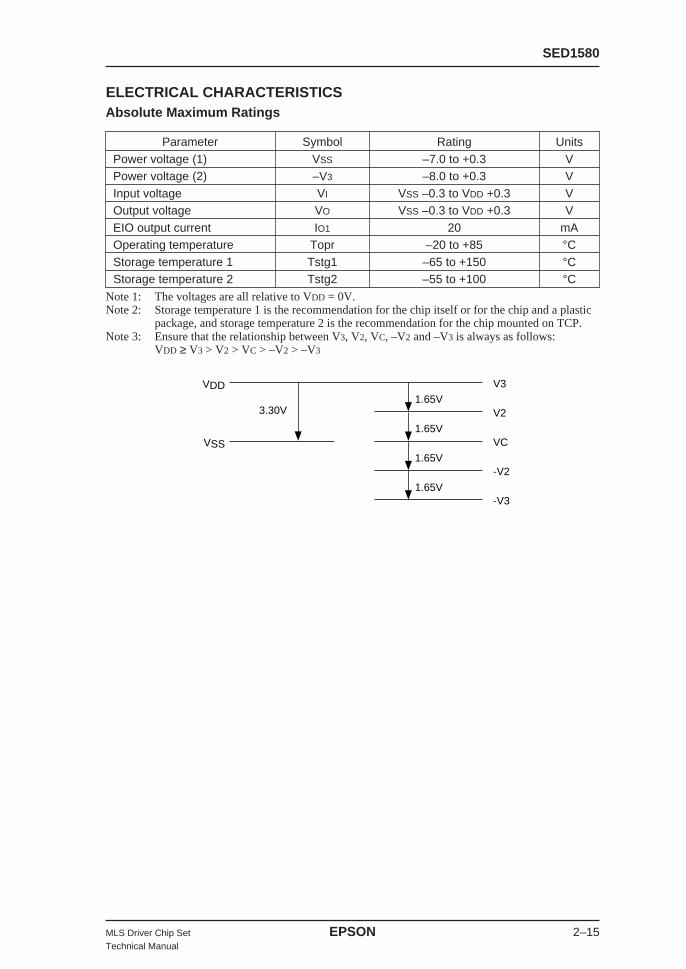
ELECTRICAL CHARACTERISTICSAbsolute Maximum Ratings
Parameter Symbol Rating UnitsPower voltage (1) VSS –7.0 to +0.3 VPower voltage (2) –V3 –8.0 to +0.3 VInput voltage VI VSS –0.3 to VDD +0.3 VOutput voltage VO VSS –0.3 to VDD +0.3 VEIO output current IO1 20 mAOperating temperature Topr –20 to +85 °CStorage temperature 1 Tstg1 –65 to +150 °CStorage temperature 2 Tstg2 –55 to +100 °C
Note 1: The voltages are all relative to VDD = 0V.Note 2: Storage temperature 1 is the recommendation for the chip itself or for the chip and a plastic
package, and storage temperature 2 is the recommendation for the chip mounted on TCP.Note 3: Ensure that the relationship between V3, V2, VC, –V2 and –V3 is always as follows:
VDD ≥ V3 > V2 > VC > –V2 > –V3
1.65V3.30V
VDD
VSS
V3
V2
VC
-V2
-V3
1.65V
1.65V
1.65V

SED1580
2–16 EPSON MLS Driver Chip SetTechnical Manual
DC Characteristics
Unless otherwise specified, VDD = V3 = 0V, VSS = –3.3V ± 0.3V, Ta = –20 to 85°CParameter Symbol Conditions Applicable Min Typ Max Units
terminals
Power voltage (1) VSS VSS –3.6 –3.3 –3.0 V
Power voltage (2) –V3 VSS = –3.0V to –3.6V –V3 –7.2 –6.4 –6.0 V
Power voltage (3) –V2 VSS = –3.0V to –3.6V –V2(–V3)* V
3/4
Power voltage (4) VC VSS = –3.0V to –3.6V VC(–V3)* V
2/4
Power voltage (5) V2 VSS = –3.0V to –3.6V V2(–V3)* V
1/4
High-level input voltage VIH EIO1, EIO2, SHL, BSEL, 0.2* VSS VVSS = LSEL, FR, YD, CA, LP,
Low-level input voltage VIL–3.3V to –3.6V XSCL, D0 to D7, F1S,
0.8* VSS VF2S, DOFF
High-level output VOHIOH = VDD – 0.4 Vvoltage VSS = –0.6mA EIO1, EIO2
Low-level output VOL–3.3V to –3.6V IOL = F1O, F2O
VSS + 0.4 Vvoltage 0.6mA
SHL, BSEL, LSEL, FR,
Input leakage current ILI VSS ≤ VIN ≤ VDDYD, CA, LP, XSCL, 5.0 µAD0 to D7, F1S, F2S,DOFF
I/O leakage current ILI/O VSS ≤ VIN ≤ VDD EIO1, EIO2 5.0 µA
Static current (1) ISSq VIN = VDD or VSS VSS 10 µA
Static current (2) –I 3T –V3 = –6.6V –V3 5 µA
∆VON = 0.5V, VSS = –3.30V,
Output resistance RSEGV3 = VDD = 0V, V2 = –1.65V, X1 to X160 0.8 1.5 KΩVC = –3.30V, –V2 = –4.95V,V3 = 6.60V
VSS = –3.30V, V3 = VDD = 0V,V2 = –1.65V, VC = –3.30V
Data –V2 = –4.95V, –V3 = –6.60VAverage Transfer ISST VIN = VDD or VSS, fXSCL = 480 kHz, VSS 70 100 µAoperating Mode fLP = 12kHz, fFR = 30Hz,consumption Input Data: checker pattern,current (1) 8-bit, 320 × 200, no load
Self XSCL = VSS Other parametersRefresh ISSS are the same as for ISST
50 70 µAMode
Average operating –I 3TParameters are the same as for –V3 10 20 µA
consumption current (2) ISST
SHL, BSEL, LSEL, FR,Input terminal CI YD, CA, LP, XSCL, 8 pFcapacitance
Freq = 1 MHzD0 to D7, F1S, F2S,
Ta = 25°CDOFF
I/O terminal CI/O Chip alone EIO1, EIO2 15 pFcapacitance
Output terminal CO F1O, F2O 7 pFcapacitance
SED1580
MLS Driver Chip Set EPSON 2–17Technical Manual
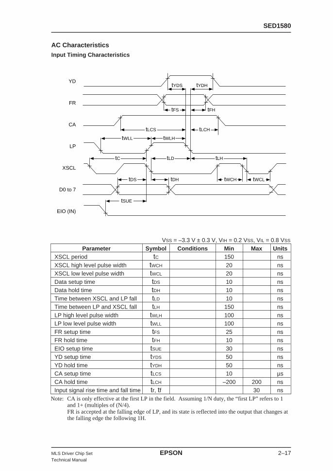
AC CharacteristicsInput Timing Characteristics
YD
FR
CA
LP
XSCL
D0 to 7
EIO (IN)
tSUE
tC tLD tLH
tLCHtLCS
tWLHtWLL
tDS
tFS
tYDHtYDS
tFH
tDH tWCH tWCL
VSS = –3.3 V ± 0.3 V, VIH = 0.2 VSS, VIL = 0.8 VSS
Parameter Symbol Conditions Min Max UnitsXSCL period tC 150 nsXSCL high level pulse width tWCH 20 nsXSCL low level pulse width tWCL 20 nsData setup time tDS 10 nsData hold time tDH 10 nsTime between XSCL and LP fall tLD 10 nsTime between LP and XSCL fall tLH 150 nsLP high level pulse width tWLH 100 nsLP low level pulse width tWLL 100 nsFR setup time tFS 25 nsFR hold time tFH 10 nsEIO setup time tSUE 30 nsYD setup time tYDS 50 nsYD hold time tYDH 50 nsCA setup time tLCS 10 µsCA hold time tLCH –200 200 nsInput signal rise time and fall time tr, tf 30 ns
Note: CA is only effective at the first LP in the field. Assuming 1/N duty, the “first LP” refers to 1and 1+ (multiples of (N/4).FR is accepted at the falling edge of LP, and its state is reflected into the output that changes atthe falling edge the following 1H.

SED1580
2–18 EPSON MLS Driver Chip SetTechnical Manual
Output Timing Characteristics
VSS = –3.3V ± 0.3V, VIH = 0.2 VSS, VIL = 0.8 VSS, –V3 = –6.6V ± 0.6V
Parameter Symbol Conditions Min Max UnitsEIO reset time tER
CL = 15 pF (EI0)80 ns
EIO output delay time tDCL 90 nsLP → Xn output delay time tLSD
CL = 100 pF400 ns
LP → F2O, F1O output delay time tLFD 3000 ns
LP
XSCL
EIO (OUT)
Xn
tLFD
tLSD
tDCL tER
F20F10
SED1580
MLS Driver Chip Set EPSON 2–19Technical Manual
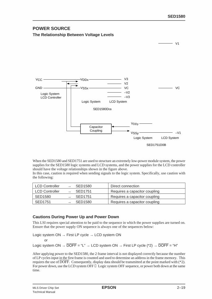
POWER SOURCEThe Relationship Between Voltage Levels
When the SED1580 and SED1751 are used to structure an extremely low-power module system, the powersupplies for the SED1580 logic systems and LCD systems, and the power supplies for the LCD controllershould have the voltage relationships shown in the figure above.In this case, caution is required when sending signals to the logic system. Specifically, use caution withthe following:
LCD Controller → SED1580 Direct connectionLCD Controller → SED1751 Requires a capacitor couplingSED1580 → SED1751 Requires a capacitor couplingSED1751 → SED1580 Requires a capacitor coupling
VDDx
VDDy
VSSy
VSSx
CapacitorCoupling
VCC
Logic SystemLCD Controller
Logic System LCD System
Logic System LCD System
V3V2VC–V2–V3
V1
VC
–V1
SED1580D0B
GND
SED1751D0B
Cautions During Power Up and Power DownThis LSI requires special attention to be paid to the sequence in which the power supplies are turned on.Ensure that the power supply ON sequence is always one of the sequences below:
Logic system ON → First LP cycle → LCD system ONor
Logic system ON → DOFF = “L” → LCD system ON → First LP cycle (*2) → DOFF = “H”
After applying power to the SED1580, the 2 frame interval is not displayed correctly because the numberof LP cycles input in the first frame is counted and used to determine an address in the frame memory. Thisrequires the use of DOFF. Consequently, display data should be transmitted at the point marked with (*2).For power down, use the LCD system OFF → Logic system OFF sequence, or power both down at the sametime.
SED1580
2–20 EPSON MLS Driver Chip SetTechnical Manual
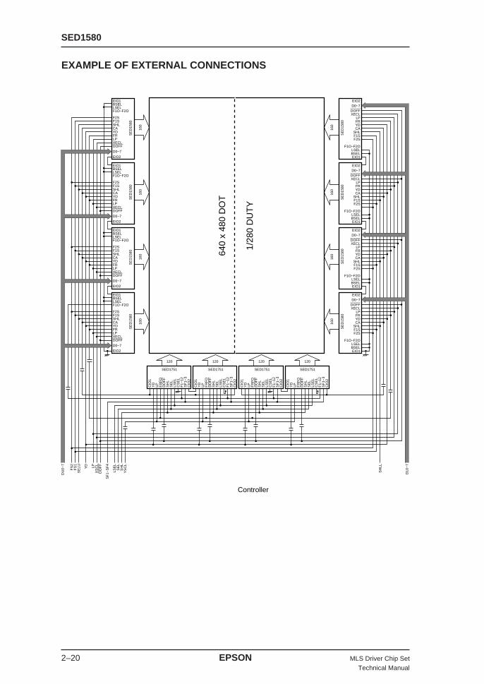
EXAMPLE OF EXTERNAL CONNECTIONS
EIO1BSELLSELF1O~F2O
F2SF1SSHLCAYDFRLPXECLDOFF
D0~7
EIO2
160
EIO1BSELLSELF1O~F2O
F2SF1SSHLCAYDFRLPXECLDOFF
D0~7
EIO2
160
EIO1BSELLSELF1O~F2O
F2SF1SSHLCAYDFRLPXECLDOFF
D0~7
EIO2
160 64
0 x
480
DO
T
1/28
0 D
UT
Y
EIO1BSELLSELF1O~F2O
F2SF1SSHLCAYDFRLPXECLDOFF
D0~7
EIO2
160
160
160
160
160
CIO
1Y
DLP F
RF
OD
OF
FS
HL
SE
LLS
EL
CS
EL
F1~
12S
F1~
3C
IO2
DU
0~7
FS
2F
S1
SE
LU YD LP
XS
CL
DO
FF
SF
1~S
F4
LSE
LS
EL
SH
LY
SC
L
SH
LL
DL0
~7
120
CIO
1Y
DLP F
RF
OD
OF
FS
HL
SE
LLS
EL
CS
EL
F1~
12S
F1~
3C
IO2
120
CIO
1Y
DLP F
RF
OD
OF
FS
HL
SE
LLS
EL
CS
EL
F1~
12S
F1~
3C
IO2
120
CIO
1Y
DLP F
RF
OD
OF
FS
HL
SE
LLS
EL
CS
EL
F1~
12S
F1~
3C
IO2
120
EIO2D0~7
DOFFXECL
LPFRYDCA
SHLF1SF2S
F1O~F2OLSELBSELEIO1
EIO2D0~7
DOFFXECL
LPFRYDCA
SHLF1SF2S
F1O~F2OLSELBSELEIO1
EIO2D0~7
DOFFXECL
LPFRYDCA
SHLF1SF2S
F1O~F2OLSELBSELEIO1
EIO2D0~7
DOFFXECL
LPFRYDCA
SHLF1SF2S
F1O~F2OLSELBSELEIO1
SE
D15
80S
ED
1580
SE
D15
80S
ED
1580
SE
D15
80S
ED
1580
SE
D15
80S
ED
1580
SED1751 SED1751 SED1751 SED1751
Controller
SED1580
MLS Driver Chip Set EPSON 2–21Technical Manual
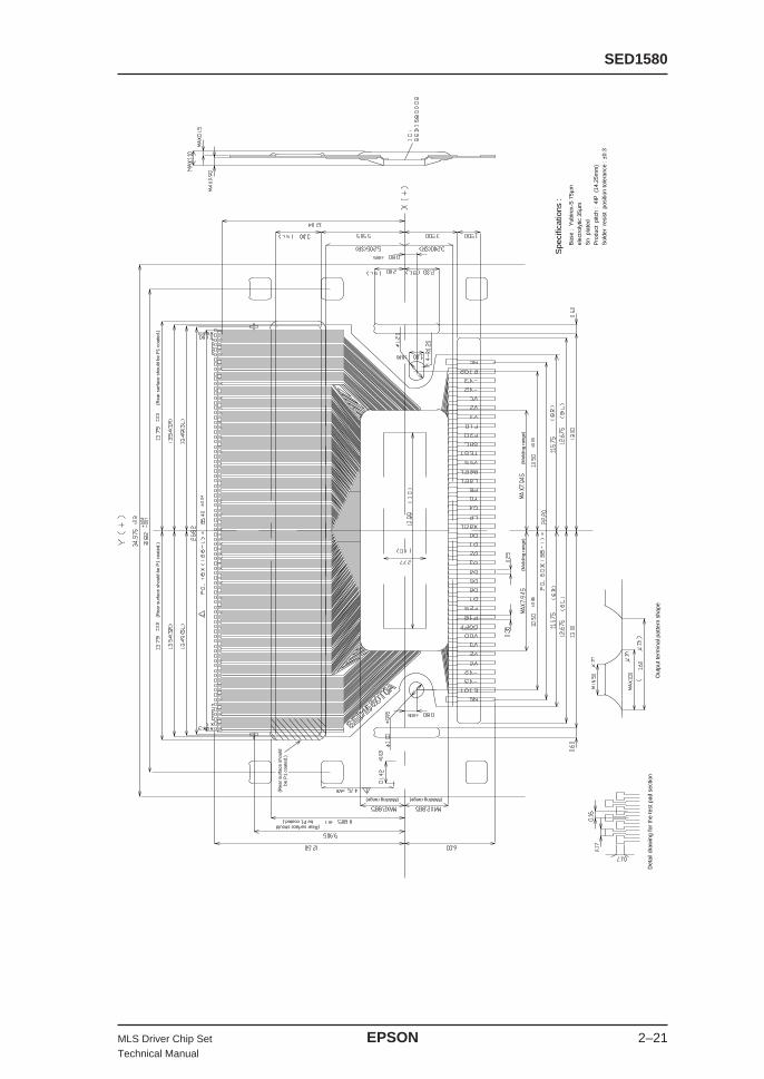
Det
ail d
raw
ing
for
the
test
pad
sec
tion
Out
put t
erm
inal
pat
tern
sha
pe
Spe
cific
atio
ns :
Bas
e :
Yub
irex-
S 7
5µm
elec
trol
ytic
35µ
m
Sn
pla
ted
Pro
duct
pitc
h :
4IP
(14
.25m
m)
Sol
der
res
ist
posi
tion
tole
ranc
e : ±
0.3
(Mol
ding
ran
ge)
(Mol
ding
ran
ge)
(Molding range) (Molding range)
(Rear surface should be P1 coated.)
(Rea
r su
rfac
e sh
ould
be
P1
coat
ed.)
(Rea
r su
rfac
e sh
ould
be
P1
coat
ed.)
(Rea
r su
rfac
e sh
ould
b
e P
1 co
ated
.)

SED1580
2–22 EPSON MLS Driver Chip SetTechnical Manual
NotesRegarding this development specification, take the followings into consideration.1. The contents of this development specification may be revised without prior notice.2. This development specification does not guarantee or grant the industrial property rights or any other
rights.The application examples contained in this development manual are given in order to help customersunderstand the product. Note that we shall not take any responsibility regarding problems on circuits.Regarding the use of semiconductor elements, take the followings into consideration.
[Precautions on Handling Optical Parts]Following the solar cell theory, the characteristics of a semiconductor element changes as it is exposed tothe light. Therefore, if this IC is exposed to the light, malfunction may occur.(1) Design and mount the IC so that it won’t be exposed to the light when in use.(2) Design and mount the IC so that it won’t be exposed to the light in the inspection process.(3) Be concerned about shading of all the surfaces (front, back and side) of the IC.
SED1590
SED1590
MLS Driver Chip Set EPSON iTechnical Manual
Contents
OVERVIEW ................................................................................................................................... 3-1
TERMINAL FUNCTIONS .............................................................................................................. 3-3
EXPLANATION OF FUNCTIONS ................................................................................................. 3-9
COMMANDS ............................................................................................................................... 3-18
ELECTRICAL CHARACTERISTICS ........................................................................................... 3-26
EXAMPLE OF USE ..................................................................................................................... 3-31
SED1590
MLS Driver Chip Set EPSON 3–1Technical Manual
OVERVIEWDescriptionThe SED 1590 is a high image quality mid-display-size-compatible RAM-integrated segment (column)driver that boasts the low power consumption required by portable devices. It is used in a set with the SED1751 common (row) driver and the SCI 7500 power supply IC.The SED 1590 can be connected directly to the MPU bus. It stores in its internal display RAM memorythe 8-bit parallel display data sent to it from the MPU and then issues the LCD drive signals independentof the MPU. The chip has 160 LCD drive outputs and is equipped with 160 out × 240 line internal displayRAM. Furthermore, because there is a one-to-one correspondence between picture elements on the LCDdisplay and internal RAM dots, displays can be created with a high degree of flexibility.Because it is not necessary to supply an external clock when writing to the SED 1590 internal RAM fromthe MPU side, these operations can be performed with an absolute minimum power consumption.Moreover, even when multiple SED 1590 chips are used, single chip select is supported; thus it is notnecessary for the MPU to distinguish between the multiple chips.The SED 1590 has a slim form that is useful in creating thinner LCD panels. It can operate using a low-voltage logic power supply system, and is thus suited to a broad range of applications.
Features• Number of LCD drive outputs: 1 ............................................. 0 out• Drive duty ratio (MAX): ................................................. 1/240 duty• RAM data displayed directly using the display data RAM.• RAM bit data (when in normal display mode): .................. "0" - Off
"1" - On• Internal RAM capacity: ............................................... 160 × 240 bit• High speed 8-bit MPU interface• Compatible with both 80x86 series and 68000 series MPUs.• Single chip select when multiple chips are used.• Rich command functions.• Extremely low consumption current.• Power supply• Logic system: ................................................................ 2.7 to 3.6 V• LCD system: .................................................................. 5.4 to 7.2 V• Non-biased display off function• Slim chip shape• Package: DIE ............................................................................. D0B
TCP .......................................................................... TXX• This product is not designed for resistance to radiation or exposure to light.

SED1590
3–2 EPSON MLS Driver Chip SetTechnical Manual
Block Diagram
CS
A0
RD
WR
C86
RES
Bus Holder
Command Decoder
MP
U Interface
F1, F2
DOFF
SLP
FR
CL
CA
M/S
VSS
VDD
V3
V2
VC
V2
V3
VEE
LR0
LR1
D7
D6
D5
D4
D3
D2
D1
D0
OSC1
OSC2
OSC3ø1· · · · · · · · · · · ·ø160
Column AddressControl Circuit
Decoder Circuit
Liquid Crystal Drive Circuit
I/O Buffer
Display DataRAM
160 x 240
MPUSystemControlCircuit
Page AddressControl Circuit
OscillatorCircuit
LCDSystemControlCircuit
StatusInput/O
utput Buffer

SED1590
MLS Driver Chip Set EPSON 3–3Technical Manual
TERMINAL FUNCTIONSTerminal Layout Diagram D 0B
DIE: D0B
Chip size: 14.82 mm × 2.50 mmBump size: 67 µm × 80 µm (min.)Bump pitch: 100 µm (min.)Bump height: 22.5 ± 5.5 µm
................................................................................................................
................................................................................................................
......
.....
...........
215
(0, 0)
76
1 59
75Y
X 60
216
231
SED1590
3–4 EPSON MLS Driver Chip SetTechnical Manual
Terminal Coordinates D0B
Pin Name X Y
1 V2 –6692 –11302 VC –65483 V2 –64044 V3 –62605 VSS –60256 OSC1 –58467 OSC2 –55888 OSC3 –52929 VSS –5016
10 NC –484711 NC –470312 CS –450713 A0 –434414 RD –418115 WR –401916 RES –385617 VSS –370318 C86 –350819 VDD –335520 LR0 –316021 VSS –300122 LR1 –280523 VDD –265224 MS –245325 VSS –229526 D0 –192627 D1 –160928 VDD –130929 D2 –105530 D3 –72831 D4 –43232 D5 –10433 D6 19134 D7 51835 FR 85836 CL 115437 VSS 141338 F1 188239 F2 217840 DOF 250641 CA 280242 SLP 319143 COD0 351944 COD1 381545 COD2 414246 COD3 443847 COD4 476648 NC 500249 NC 514650 NC 529051 NC 543452 NC 557853 NC 572254 NC 586655 NC 601056 V3 626057 V2 640458 VC 6548
Pin Name X Y
59 V2 6692 –113060 V3 7290 –83761 VEE –69362 NC –54963 NC –36964 O160 –26865 O159 –16766 O158 –6667 O157 3368 O156 13469 O155 23570 O154 33671 O153 43772 O152 53773 O151 63874 O150 73975 NC 84076 NC 7007 113077 O149 690478 O148 680479 O147 670380 O146 660281 O145 650182 O144 640083 O143 630084 O142 619985 O141 609886 O140 599787 O139 589688 O138 579689 O137 569590 O136 559491 O135 549392 O134 539293 O133 529294 O132 519195 O131 509096 O130 498997 O129 488898 O128 478899 O127 4687100 O126 4586101 O125 4485102 O124 4384103 O123 4284104 O122 4183105 O121 4082106 O120 3981107 O119 3880108 O118 3780109 O117 3679110 O116 3578111 O115 3477112 O114 3376113 O113 3276114 O112 3175115 O111 3074116 O110 2973

SED1590
MLS Driver Chip Set EPSON 3–5Technical Manual
117 O109 2872 1130118 O108 2772119 O107 2671120 O106 2570121 O105 2469122 O104 2368123 O103 2268124 O102 2167125 O101 2066126 O100 1965127 O99 1864128 O98 1764129 O97 1663130 O96 1562131 O95 1461132 O94 1360133 O93 1260134 O92 1159135 O91 1058136 O90 957137 O89 856138 O88 756139 O87 655140 O86 554141 O85 453142 O84 352143 O83 252144 O82 151145 O81 50146 O80 –50147 O79 –151148 O78 –252149 O77 –352150 O76 –453151 O75 –554152 O74 –655153 O73 –756154 O72 –856155 O71 –957156 O70 –1058157 O69 –1159158 O68 –1260159 O67 –1360160 O66 –1461161 O65 –1562162 O64 –1663163 O63 –1764164 O62 –1864165 O61 –1965166 O60 –2066167 O59 –2167168 O58 –2268169 O57 –2368170 O56 –2469171 O55 –2570172 O54 –2671173 O53 –2772174 O52 –2872
Pin Name X Y
175 O51 –2973 1130176 O50 –3074177 O49 –3175178 O48 –3276179 O47 –3376180 O46 –3477181 O45 –3578182 O44 –3679183 O43 –3780184 O42 –3880185 O41 –3981186 O40 –4082187 O39 –4183188 O38 –4284189 O37 –4384190 O36 –4485191 O35 –4586192 O34 –4687193 O33 –4788194 O32 –4888195 O31 –4989196 O30 –5090197 O29 –5191198 O28 –5292199 O27 –5392200 O26 –5493201 O25 –5594202 O24 –5695203 O23 –5796204 O22 –5896205 O21 –5997206 O20 –6098207 O19 –6199208 O18 –6300209 O17 –6400210 O16 –6501211 O15 –6602212 O14 –6703213 O13 –6804214 O12 –6904215 NC –7007216 NC –7290 840217 O11 739218 O10 638219 O9 537220 O8 437221 O7 336222 O6 235223 O5 134224 O4 33225 O3 –66226 O2 –167227 O1 –268228 NC –369229 NC –549230 VEE –693231 V3 –837
Pin Name X Y

SED1590
3–6 EPSON MLS Driver Chip SetTechnical Manual
Explanation of TerminalsPower Supply Terminals
Terminals Pertaining to the MPU
TerminalI/O Explanation
No. ofName Terminals
VDD Power Supply These are connected to VCC 3(the system power supply).
VSS Power Supply These are connected to the system GND. 6
VEE Power Supply These are the liquid crystal drive system load-side 2power supplies. VDD–VEE.
V3, V2, VC, Power Supply These are the liquid crystal drive multi-level power 2 Each–V2, –V3 supplies. The relationships between the various levels
must be: VDD ≥ V3 ≥ V2 ≥ VC > –V2 > –V3 ≥ VEE
TerminalI/O Explanation
No. ofName Terminals
D7 to D0 I These comprise the 8–bit bi-directional data bus, and are connected 8to a standard 8–bit or 16–bit MPU data bus.
A0 I The least significant bit of the address bus of a normal MPU is 1connected to discern between data and commands.H: Inidcates that D7 to D0 are control data.L: Indicates that D7 to D0 are display data.
RES I When initial settings are restored by placing RES to “L”. 1The reset operation is performed based on the RES level.Schmidt trigger.
CS I This is the chip select signal. In the SED 1590, even if multiple 1chips are used, the CS is a shared line. When CS is in a non-activestate, D7 to D0 enter a high-impedance state.
RD (E) I • When connected to an 80x86 series MPU 1Active “L”This terminal connects to the RD signal of the 80x86 MPU,and while this signal is low, the data bus is in an output state.
• When connected to a 68000 series MPUActive “H”This serves as the 68000 MPU-enabled clock input terminal.
WR I • When connected to an 80x86 system MPU 1(R/W) Active “L”
This terminal is connected to the WR signal of the 80x86 seriesMPU. The data bus signals are latched on the rising edge ofthe WR signal.
• When connected to a 68000 series MPUThis is the read/write control input terminal.R/W = “H”: ReadR/W = “L”: Write
C86 I This is the MPU interface switch terminal. 1C86 = “H”: The 68000 MPU interface.C86 = “L”: The 80x86 series MPU interface.
SED1590
MLS Driver Chip Set EPSON 3–7Technical Manual
Liquid Crystal Drive Circuit Signals
TerminalI/O Explanation
No. ofName Terminals
OSC1 I This is for the oscillator circuit. When an external input is used, 1it is input to this terminal. Connect to “H” or “L” in case of slaveoperations.
OSC2 O This is a terminal for the oscillator circuit. When the internal 1oscillator circuit is used, connect to OSC1 through a capacitor. Makethis terminal open in case of slave operations.
OSC3 O This is a terminal for the oscillator circuit. When the internal 1oscillator circuit is used, connect to OSC1 through a resistor. Makethis terminal open in case of slave operations.
M/S I/O This terminal selects master/slave operation. In master mode, 1signals required for the liquid crystal display are output, while duringslave operation signals that are required to the liquid crystaldisplay are input, thereby synchronizing the liquid crystal displaysystem.
M/S = “H”: Master operationM/S = “L”: Slave operation
CL I/O This is the display clock input/output terminal. When using 1master/slave mode, this is connected to the various CL terminals.This is also connected to the common driver YSCL terminals.
When M/S = “H”: OutputWhen M/S = “L”: Input
FR I/O This is the liquid crystal alternating current input/output terminal. 1When using master/slave mode, this is connected to the variousFR terminals. This is also connected to the common driver FRterminals.
When M/S = “H”: OutputWhen M/S = “L”: Input
CA I/O This is the field start signal. When using master/slave mode, this is 1connected to the various CA terminals. This is also connected to thecommon driver CA terminals.
When M/S = “H”: OutputWhen M/S = “L”: Input
DOF I/O This is the liquid crystal display blanking control terminal. 1When using master/slave mode, this is connected to the variousDOFF terminals. This is also connected to the common driverDOFF terminals.
When M/S = “H”: OutputWhen M/S = “L”: Input
SLP O This is the sleep control terminal. When set to a sleep status by the 1MCU, both the master and the slave circuits enter the sleep mode.This terminal is not connected between the master and the slave.Connect to the SCI 7500 SLP terminal for the master only.
F1, F2 I/O These are the drive pattern signal input/output terminals. 1 eachWhen in master/slave mode, these are connected to the F1and F2 terminals respectively. These are connected to thecommon driver F1 and F2 terminals.
When M/S = “H”: OutputWhen M/S = “L”: Input
On O Liquid crystal segment drive outputs 160
SED1590
3–8 EPSON MLS Driver Chip SetTechnical Manual
Control Terminals
TerminalI/O Explanation
No. ofName Terminals
LR0, LR1 I When multiple SED1590 chips are used, these terminals 1 eachspecify the various segment driver layout positions. Using thisinformation, the SED1590 determines the relationshipsbetween the various segments and the position in internal RAM.
COD0COD1
These comprise the 5–bit output port. The status of this port can be
COD2 Ocontrolled by commands from the MPU.
1 eachCOD3
They can be used for controls of the electronic volume control
COD4knobs and other applications.

SED1590
MLS Driver Chip Set EPSON 3–9Technical Manual
EXPLANATION OF FUNCTIONSThe MPU InterfaceThe SED1590 exchanges data with the MPU through an 8–bit bi-directional data bus (D7 to D0).By setting the C86 terminal to “H” or “L” the SED1590 can be connected directly to the MPU bus for eitherthe 80x86 system MPUs or the 68000 system MPUs, as shown in Table 1.
The SED1590 identifies data bus signals using combinations of the A0, E, R/W and (RD, WR) signals asshown in Table 2.
The SED1590 possesses a function that automatically identifies the segment driver position by the LR0and LR1 terminals even when multiple SED1590 chips are used, so from the perspective of the MPU, thereis no need for the MPU to identify the individual segment drivers. As a result, the CS chip select terminalscan share a common line from the outside. The LR will be discussed below.When the chips are not selected, D0 to D7 enter a high impedance state and terminals A0, RD, and WRinputs are disabled.
Accessing the Display Data RAM and the Internal Registers.The SED1590 uses a type of pipeline process between LSIs through the bus holders in the internal data busin order to match the operating frequencies between the MPU and the display data RAM and internalregisters. Consequently, when viewed from the MPU side, there are no constraints on accessing theSED1590 in terms of the display data RAM access time (tACC), but rather the cycle time is dominant. Whenthe cycle time is not adequate, then the MPU may insert an NOP command, which is equivalent to executinga dummy wait.
Table 1
C86 Type CS A0 RD WR D0 to D7
H 68000 MPU bus CS A0 E R/W D0 to D7
L 80×86 MPU bus CS A0 RD WR D0 to D7
Common 68 System 80 SystemA0 R/W RD WR Function1 0 1 0 Write display data0 1 0 1 Read status0 0 1 0 Write to internal register (command)
Table 2

SED1590
3–10 EPSON MLS Driver Chip SetTechnical Manual
• Writing
• Reading
WR
Command Write Data Write Data Write
DATA
BusHolder
MCU
InternalWrite
Signal
tcyc
RD
WR
DATA
Data Read
Command Write
BusHolder
MCU
InternalRead
Signal
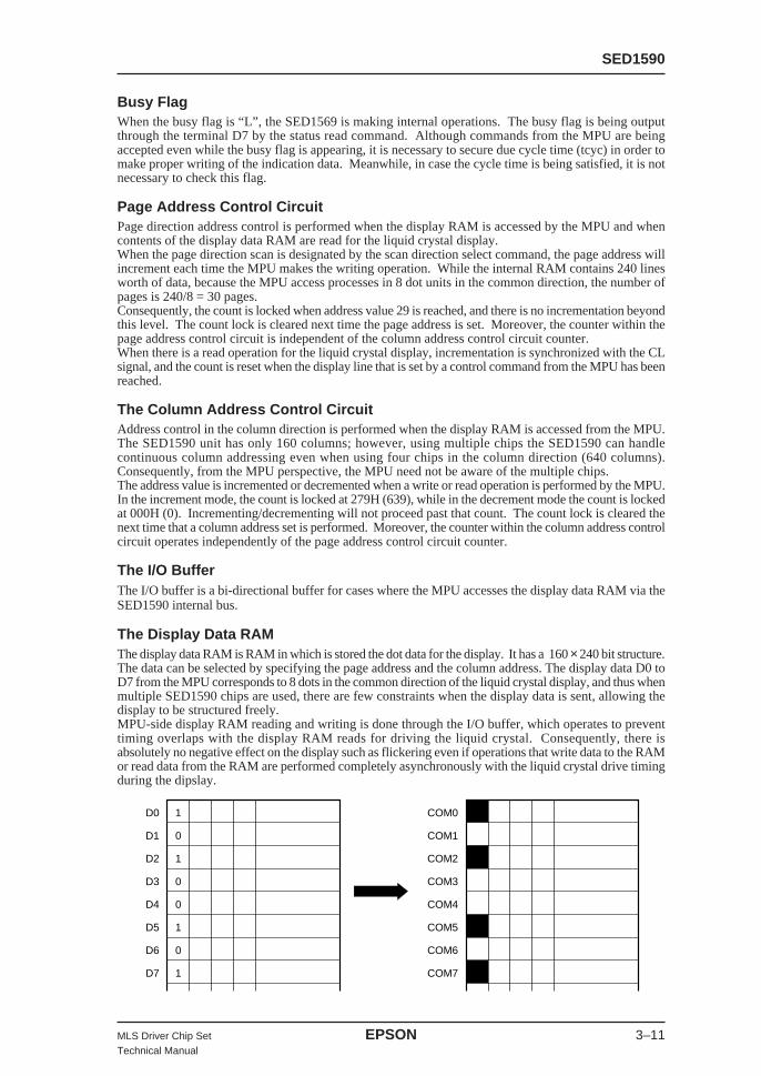
SED1590
MLS Driver Chip Set EPSON 3–11Technical Manual
Busy FlagWhen the busy flag is “L”, the SED1569 is making internal operations. The busy flag is being outputthrough the terminal D7 by the status read command. Although commands from the MPU are beingaccepted even while the busy flag is appearing, it is necessary to secure due cycle time (tcyc) in order tomake proper writing of the indication data. Meanwhile, in case the cycle time is being satisfied, it is notnecessary to check this flag.
Page Address Control CircuitPage direction address control is performed when the display RAM is accessed by the MPU and whencontents of the display data RAM are read for the liquid crystal display.When the page direction scan is designated by the scan direction select command, the page address willincrement each time the MPU makes the writing operation. While the internal RAM contains 240 linesworth of data, because the MPU access processes in 8 dot units in the common direction, the number ofpages is 240/8 = 30 pages.Consequently, the count is locked when address value 29 is reached, and there is no incrementation beyondthis level. The count lock is cleared next time the page address is set. Moreover, the counter within thepage address control circuit is independent of the column address control circuit counter.When there is a read operation for the liquid crystal display, incrementation is synchronized with the CLsignal, and the count is reset when the display line that is set by a control command from the MPU has beenreached.
The Column Address Control CircuitAddress control in the column direction is performed when the display RAM is accessed from the MPU.The SED1590 unit has only 160 columns; however, using multiple chips the SED1590 can handlecontinuous column addressing even when using four chips in the column direction (640 columns).Consequently, from the MPU perspective, the MPU need not be aware of the multiple chips.The address value is incremented or decremented when a write or read operation is performed by the MPU.In the increment mode, the count is locked at 279H (639), while in the decrement mode the count is lockedat 000H (0). Incrementing/decrementing will not proceed past that count. The count lock is cleared thenext time that a column address set is performed. Moreover, the counter within the column address controlcircuit operates independently of the page address control circuit counter.
The I/O BufferThe I/O buffer is a bi-directional buffer for cases where the MPU accesses the display data RAM via theSED1590 internal bus.
The Display Data RAMThe display data RAM is RAM in which is stored the dot data for the display. It has a 160 × 240 bit structure.The data can be selected by specifying the page address and the column address. The display data D0 toD7 from the MPU corresponds to 8 dots in the common direction of the liquid crystal display, and thus whenmultiple SED1590 chips are used, there are few constraints when the display data is sent, allowing thedisplay to be structured freely.MPU-side display RAM reading and writing is done through the I/O buffer, which operates to preventtiming overlaps with the display RAM reads for driving the liquid crystal. Consequently, there isabsolutely no negative effect on the display such as flickering even if operations that write data to the RAMor read data from the RAM are performed completely asynchronously with the liquid crystal drive timingduring the dipslay.
D0
D1
D2
D3
D4
D5
D6
D7
1
0
1
0
0
1
0
1
COM0
COM1
COM2
COM3
COM4
COM5
COM6
COM7
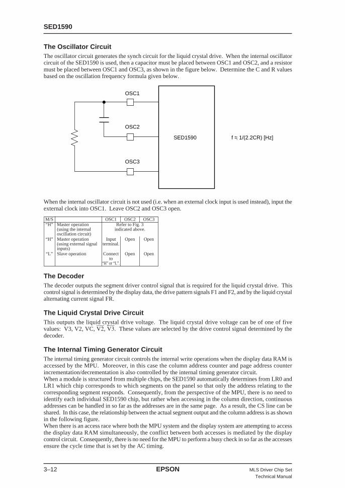
SED1590
3–12 EPSON MLS Driver Chip SetTechnical Manual
The Oscillator CircuitThe oscillator circuit generates the synch circuit for the liquid crystal drive. When the internal oscillatorcircuit of the SED1590 is used, then a capacitor must be placed between OSC1 and OSC2, and a resistormust be placed between OSC1 and OSC3, as shown in the figure below. Determine the C and R valuesbased on the oscillation frequency formula given below.
When the internal oscillator circuit is not used (i.e. when an external clock input is used instead), input theexternal clock into OSC1. Leave OSC2 and OSC3 open.
The DecoderThe decoder outputs the segment driver control signal that is required for the liquid crystal drive. Thiscontrol signal is determined by the display data, the drive pattern signals F1 and F2, and by the liquid crystalalternating current signal FR.
The Liquid Crystal Drive CircuitThis outputs the liquid crystal drive voltage. The liquid crystal drive voltage can be of one of fivevalues: V3, V2, VC, V2, V3. These values are selected by the drive control signal determined by thedecoder.
The Internal Timing Generator CircuitThe internal timing generator circuit controls the internal write operations when the display data RAM isaccessed by the MPU. Moreover, in this case the column address counter and page address counterincrementation/decrementation is also controlled by the internal timing generator circuit.When a module is structured from multiple chips, the SED1590 automatically determines from LR0 andLR1 which chip corresponds to which segments on the panel so that only the address relating to thecorresponding segment responds. Consequently, from the perspective of the MPU, there is no need toidentify each individual SED1590 chip, but rather when accessing in the column direction, continuousaddresses can be handled in so far as the addresses are in the same page. As a result, the CS line can beshared. In this case, the relationship between the actual segment output and the column address is as shownin the following figure.When there is an access race where both the MPU system and the display system are attempting to accessthe display data RAM simultaneously, the conflict between both accesses is mediated by the displaycontrol circuit. Consequently, there is no need for the MPU to perform a busy check in so far as the accessesensure the cycle time that is set by the AC timing.
OSC1
OSC2
OSC3
SED1590 f = 1/(2.2CR) [Hz]..
M/S OSC1 OSC2 OSC3“H” Master operation Refer to Fig. 3
(using the internal indicated above.oscillation circuit)
“H” Master operation Input Open Open(using external signal terminal.inputs)
“L” Slave operation Connect Open Opento
“H” or “L”.
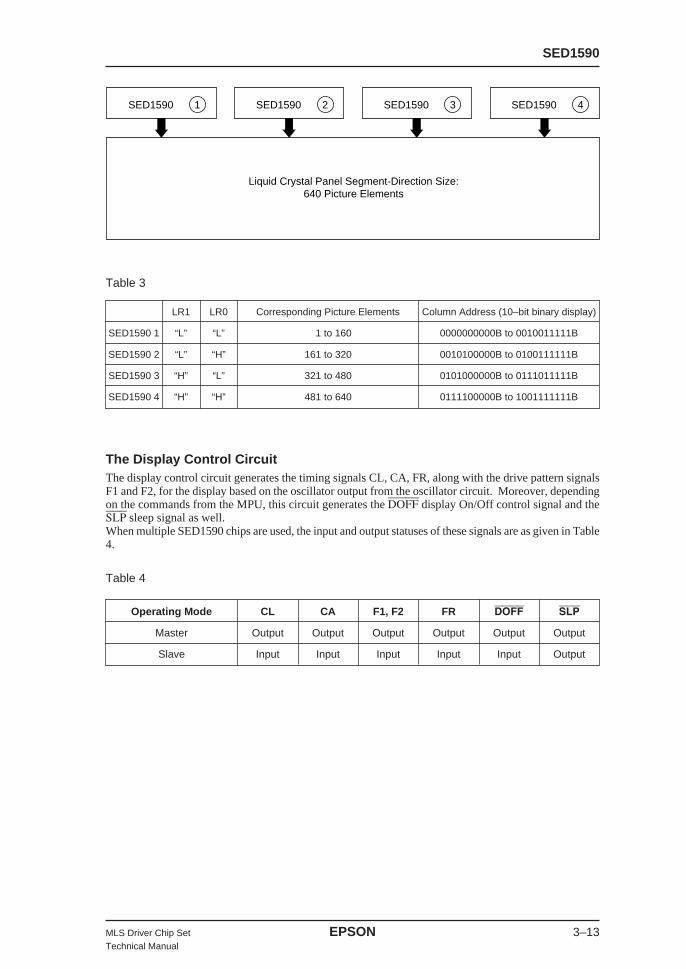
SED1590
MLS Driver Chip Set EPSON 3–13Technical Manual
Table 3
The Display Control CircuitThe display control circuit generates the timing signals CL, CA, FR, along with the drive pattern signalsF1 and F2, for the display based on the oscillator output from the oscillator circuit. Moreover, dependingon the commands from the MPU, this circuit generates the DOFF display On/Off control signal and theSLP sleep signal as well.When multiple SED1590 chips are used, the input and output statuses of these signals are as given in Table4.
Table 4
SED1590 1 SED1590
Liquid Crystal Panel Segment-Direction Size:640 Picture Elements
2 SED1590 3 SED1590 4
Operating Mode CL CA F1, F2 FR DOFF SLP
Master Output Output Output Output Output Output
Slave Input Input Input Input Input Output
LR1 LR0 Corresponding Picture Elements Column Address (10–bit binary display)
SED1590 1 “L” “L” 001 to 160 0000000000B to 0010011111B
SED1590 2 “L” “H” 161 to 320 0010100000B to 0100111111B
SED1590 3 “H” “L” 321 to 480 0101000000B to 0111011111B
SED1590 4 “H” “H” 481 to 640 0111100000B to 1001111111B
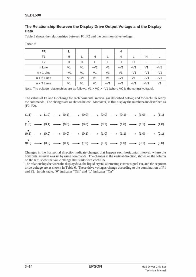
SED1590
3–14 EPSON MLS Driver Chip SetTechnical Manual
The Relationship Between the Display Drive Output Voltage and the DisplayDataTable 5 shows the relationships between F1, F2 and the common drive voltage.
Table 5
The values of F1 and F2 change for each horizontal interval (as described below) and for each CA set bythe commands. The changes are as shown below. Moreover, in this display the numbers are described as(F2, F2).
Changes in the horizontal direction indicate changes that happen each horizontal interval, where thehorizontal interval was set by using commands. The changes in the vertical direction, shown on the columnon the left, show the value change that starts with each CA.The relationships between the display data, the liquid crystal alternating current signal FR, and the segmentdrive voltage are as shown in Table 6. These drive voltages change according to the combination of F1and F2. In this table, “0” indicates “Off” and “1” indicates “On”.
FR L H
F1 H L H L H L H L
F2 H H L L H H L L
n Line V1 V1 –V1 V1 –V1 –V1 V1 –V1
n + 1 Line –V1 V1 V1 V1 V1 –V1 –V1 –V1
n + 2 Lines V1 –V1 V1 V1 –V1 V1 –V1 –V1
n + 3 Lines V1 V1 V1 –V1 –V1 –V1 –V1 V1
Note: The voltage relationships are as follows: V1 > VC > –V1 (where VC is the central voltage).
(1,1) (1,0) (0,1) (0,0) (0,0) (0,1) (1,0) (1,1)
(1,0) (0,1) (0,0) (0,0) (0,1) (1,0) (1,1) (1,0)
(0,1) (0,0) (0,0) (0,1) (1,0) (1,1) (1,0) (0,1)
(0,0) (0,0) (0,1) (1,0) (1,1) (1,0) (0,1) (0,0)
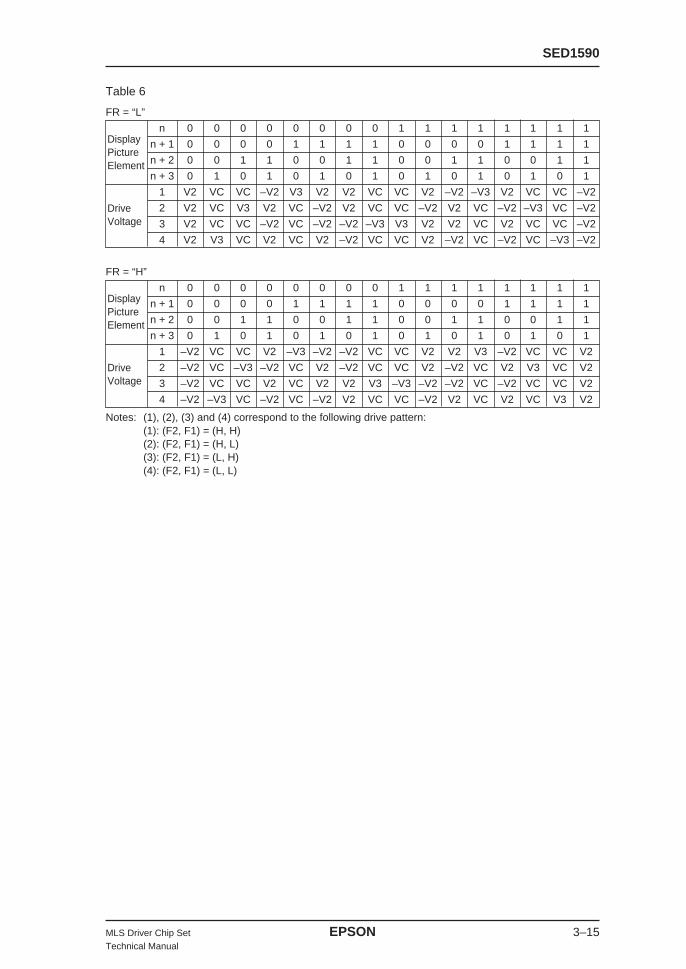
SED1590
MLS Driver Chip Set EPSON 3–15Technical Manual
Table 6
FR = “L”
n 0 0 0 0 0 0 0 0 1 1 1 1 1 1 1 1
n + 1 0 0 0 0 1 1 1 1 0 0 0 0 1 1 1 1
n + 2 0 0 1 1 0 0 1 1 0 0 1 1 0 0 1 1
n + 3 0 1 0 1 0 1 0 1 0 1 0 1 0 1 0 1
1 V2 VC VC –V2 V3 V2 V2 VC VC V2 –V2 –V3 V2 VC VC –V2
2 V2 VC V3 V2 VC –V2 V2 VC VC –V2 V2 VC –V2 –V3 VC –V2
3 V2 VC VC –V2 VC –V2 –V2 –V3 V3 V2 V2 VC V2 VC VC –V2
4 V2 V3 VC V2 VC V2 –V2 VC VC V2 –V2 VC –V2 VC –V3 –V2
FR = “H”
n 0 0 0 0 0 0 0 0 1 1 1 1 1 1 1 1
n + 1 0 0 0 0 1 1 1 1 0 0 0 0 1 1 1 1
n + 2 0 0 1 1 0 0 1 1 0 0 1 1 0 0 1 1
n + 3 0 1 0 1 0 1 0 1 0 1 0 1 0 1 0 1
1 –V2 VC VC V2 –V3 –V2 –V2 VC VC V2 V2 V3 –V2 VC VC V2
2 –V2 VC –V3 –V2 VC V2 –V2 VC VC V2 –V2 VC V2 V3 VC V2
3 –V2 VC VC V2 VC V2 V2 V3 –V3 –V2 –V2 VC –V2 VC VC V2
4 –V2 –V3 VC –V2 VC –V2 V2 VC VC –V2 V2 VC V2 VC V3 V2
Notes: (1), (2), (3) and (4) correspond to the following drive pattern:(1): (F2, F1) = (H, H)(2): (F2, F1) = (H, L)(3): (F2, F1) = (L, H)(4): (F2, F1) = (L, L)
DisplayPictureElement
DriveVoltage
DisplayPictureElement
DriveVoltage
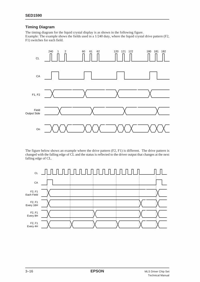
SED1590
3–16 EPSON MLS Driver Chip SetTechnical Manual
Timing DiagramThe timing diagram for the liquid crystal display is as shown in the following figure.Example: The example shows the fields used in a 1/240 duty, where the liquid crystal drive pattern (F2,F1) switches for each field.
240
CL
CA
F1, F2
On
FieldOutput Side
1 2 60 61 62 120 121 122 180 181 182
The figure below shows an example where the drive pattern (F2, F1) is different. The drive pattern ischanged with the falling edge of CL and the status is reflected to the driver output that changes at the nextfalling edge of CL.
F2, F1Every 4H
F2, F1Every 8H
F2, F1Every 16H
F2, F1Each Field
CA
CL
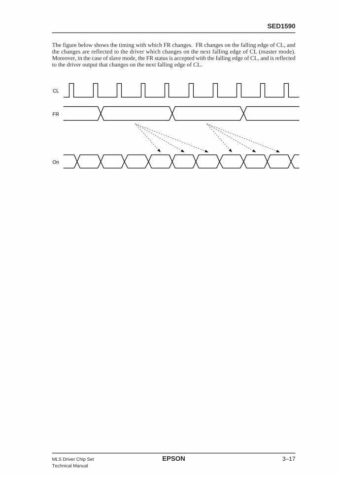
SED1590
MLS Driver Chip Set EPSON 3–17Technical Manual
The figure below shows the timing with which FR changes. FR changes on the falling edge of CL, andthe changes are reflected to the driver which changes on the next falling edge of CL (master mode).Moreover, in the case of slave mode, the FR status is accepted with the falling edge of CL, and is reflectedto the driver output that changes on the next falling edge of CL.
On
FR
CL
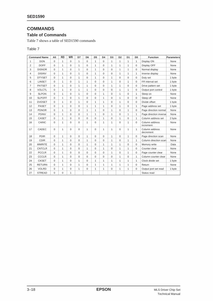
SED1590
3–18 EPSON MLS Driver Chip SetTechnical Manual
COMMANDSTable of CommandsTable 7 shows a table of SED1590 commands
Table 7
Command Name A0 RD WR D7 D6 D5 D4 D3 D2 D1 D0 Function Parameters
1 DON 0 1 0 1 0 1 0 1 1 1 1 Display ON None
2 DOFF 0 1 0 1 0 1 0 1 1 1 0 Display OFF None
3 DISNOR 0 1 0 1 0 1 0 0 1 1 0 Normal display None
4 DISINV 0 1 0 1 0 1 0 0 1 1 1 Inverse display None
5 DTYSET 0 1 0 1 0 1 0 1 0 0 0 Duty set 1 byte
6 LINSET 0 1 0 1 1 0 0 1 0 1 0 FR interval set 1 byte
7 PATSET 0 1 0 1 1 0 0 1 1 0 0 Drive pattern set 1 byte
8 VOLCTL 0 1 0 1 1 0 0 0 1 1 0 Output port control 1 byte
9 SLPON 0 1 0 1 0 0 1 0 1 0 1 Sleep on None
10 SLPOFF 0 1 0 1 0 0 1 0 1 0 0 Sleep off None
11 DVDSET 0 1 0 1 0 1 1 0 1 0 0 Divide offset 1 byte
12 PASET 0 1 0 0 1 1 1 0 1 0 1 Page address set 1 byte
13 PDNOR 0 1 0 0 1 1 0 1 0 1 0 Page direction normal None
14 PDINV 0 1 0 0 1 1 0 1 0 1 1 Page direction inverse None
15 CASET 0 1 0 0 0 0 1 0 1 0 1 Column address set 2 byte
16 CAINC 0 1 0 0 1 0 1 1 0 1 0 Column address Noneincrement
17 CADEC 0 1 0 0 1 0 1 1 0 1 1 Column address Nonedecrement
18 PDIR 0 1 0 0 1 0 0 1 0 1 0 Page direction scan None
19 CDIR 0 1 0 0 1 0 0 1 0 1 1 Column direction scan None
20 MWRITE 0 1 0 0 1 0 1 1 1 0 0 Memory write Data
21 CNTCLR 0 1 0 0 1 0 1 0 1 1 0 Counter clear None
22 PCCLR 0 1 0 0 0 0 0 1 0 1 0 Page counter clear None
23 CCCLR 0 1 0 0 0 0 0 0 1 0 1 Column counter clear None
24 CKSET 0 1 0 1 0 1 1 1 1 1 1 Clock divide set 1 byte
25 RETURN 0 1 0 1 0 1 1 1 1 1 0 Return None
26 VOLRD 0 1 0 1 0 1 1 0 1 1 0 Output port set read 1 byte
27 STREAD 0 0 1 Status read
SED1590
MLS Driver Chip Set EPSON 3–19Technical Manual
Command DetailsThe SED1590 identifies the data bus signals by a combination of A0, RD (E), WR (R/W). The commandinterpretation and execution is performed based entirely on internal timing without relying on any externalclock.In the 80×86 MPU interface, a low pulse is sent to the WR terminal to launch the command when writing.In the 68000 series MPU interface, a “L” input to the R/W terminal causes a write state, and then thecommands are launched when a high pulse input is sent to the E terminal. Consequently, the 68000 seriesMPU interface is different from the 80x86 MPU interface in the command details and command tables,and in that the RD (E) terminal is “1” (“H”) when performing status reads and when reading display data.The commands will be explained below using the 80×86 MPU interface in the examples.
Display ON/OFF Command: 1, Parameter:0
This command forces the entire display ON or OFF. When the display is OFF, all outputs are fixed at VC.Because the display is not possible when in sleep mode, make sure that this command is used after the sleepmode is turned OFF.
Page Address Set Command: 1, Parameter: 1
This command and its following parameters makes it possible to set the page address corresponding to thelow address when accessing the display data RAM from the MPU side. The desired bit of the display dataRAM can be accessed by specifying the page address and the column address. The page addresses are 5bits, corresponding to 30 pages (pages 0 to 29). Even if the page address changes, there is no change tothe display status.This command is input into the registers and loaded in the counters). That which is input is stored withinthe register, and can be reloaded by the PACLR command.
Page Address Direction Command: 1, Parameter: 0
This command makes it possible to reverse the position of page 0 in the page address of the display RAMdata. Consequently, it is possible to reverse the page address scan direction when the MPU uses the displaydata in the page direction. The relationship between the physical position in internal RAM and the pageaddress is inverted:Normal: 0 → 29Reversed: 24 ← 0When reversed, the final page address becomes 24. Consequently, the number of lines which can beindicated becomes upto 200.
Command Name A0 RD WR D7 D6 D5 D4 D3 D2 D1 D0 Function
DON 0 1 0 1 0 1 0 1 1 1 1 Display ON
DOFF 0 1 0 1 0 1 0 1 1 1 0 Display OFF
Command Name A0 RD WR D7 D6 D5 D4 D3 D2 D1 D0 Function
PASET 0 1 0 0 1 1 1 0 1 0 1 Page address set
Parameter 1 1 0 D D D D D
Command Name A0 RD WR D7 D6 D5 D4 D3 D2 D1 D0 Function
PDNOR 0 1 0 0 1 1 0 1 0 1 0 Page direction normal
PDINV 0 1 0 0 1 1 0 1 0 1 1 Page direction inverted
SED1590
3–20 EPSON MLS Driver Chip SetTechnical Manual
Column Address Set Command: 1, Parameter: 2
Column Address Direction Command: 1, Parameters: 0
This command specifies the behavior of the column address counter (increment vs. decrement).The address increments or decrements each time RAM accesses the display data. In the increment mode,the count operation stops when the value reaches 279H (639), or when the value reaches 000H (0) in thedecrement mode.
Scan Direction Select Command: 1, Parameter: 0
When the MPU continuously accesses display memory, this determines whether the scanning will be donein the page direction or in the column direction.
This command and its following parameters make it possible to specify the column address when the MPUaccesses display data RAM in the column direction. The desired bit of display data RAM can be accessedby specifying the page address and the column address. The column address has 10 bits, and when fourof the chips are used in the column direction, up to 640 dots (pixels) are supported. Even when the addresschanges, the state of the display does not change. There are 640 columns (columns 0 to 639).The address value is input with the less significant address 5 bit first and then the more significant 5 bit.With the less significant alone, when another command is entered, only the less significant is entered intothe register, however, the counter is not loaded. When the less significant is followed by the moresignificant, they are loaded into the counter and the input is stored in the register. When the less significantaddress is followed by some other command, the counter will not be loaded and the command will becancelled. With this command, the set values can be reloaded by the CCCLR command.
Command Name A0 RD WR D7 D6 D5 D4 D3 D2 D1 D0 Function
CASET 0 1 0 0 0 0 1 0 1 0 1 Column address set
Parameter 1 1 1 0 D D D D D Lower 5 bits
Parameter 2 1 1 0 D D D D D Upper 5 bits
Command Name A0 RD WR D7 D6 D5 D4 D3 D2 D1 D0 Function
CAINC 0 1 0 0 1 0 1 1 0 1 0 Column addressincrement
CADEC 0 1 0 0 1 0 1 1 0 1 1 Column addressdecrement
Command Name A0 RD WR D7 D6 D5 D4 D3 D2 D1 D0 Function
PDIR 0 1 0 0 1 0 0 1 0 1 0 Page direction scan
CDIR 0 1 0 0 1 0 0 1 0 1 1 Column direction scan
SED1590
MLS Driver Chip Set EPSON 3–21Technical Manual
Status Read
This read operation makes it possible to monitor the internal operating status of the SED1590.No other command except for the status read command will be accepted with a RAM busy state (1). If thecycle time is followed, then there is no need to check for the RAM busy state under normal use.
Display Data Write Command: 1, Parameter: Number of data to be written
When the MPU writes data to the memory, this command places the chip in a data entry mode. By writingdata again after this command, the display data RAM contents can be changed. The data write mode iscleared automatically when another command is entered.
Command Name A0 RD WR D7 D6 D5 D4 D3 D2 D1 D0 Function
MWRITE 0 1 0 0 1 0 1 1 1 0 0 Memory write
Parameter 1 1 0 D D D D D D D D Write data
Command Name A0 RD WR D7 D6 D5 D4 D3 D2 D1 D0 Function
STREAD 0 0 1 O O O O O O O O Status
D7: Busy/Ready Busy: 1, Ready: 0
D6: Page Address Direction Normal: 1, Inverted: 0
D5: Column Address Direction Normal: 1, Inverted:0
D4: Increment Direction Column: 0, Page: 1
D3: Display ON/OFF Off: 1, On: 0
D2: SLEEP ON/OFF Off: 0, On: 1
D1: INVERT Normal Display: 1, Invert Display: 0
D0: Reserved terminal

SED1590
3–22 EPSON MLS Driver Chip SetTechnical Manual
Duty Set Command: 1, Parameter: 1
This command combined with the following paramenter sets the duty.
Sleep Mode On/Off Command: 1, Parameter:0
This command controls the sleep mode of the LCD module. Before launching this command, be sure thatthe Display OFF command has been entered and that the display is in an OFF state. Moreover, after issuingthe Sleep OFF command, be sure to maintain the logic power supply for 40 ms to discharge the load of thepower supply IC.
Display Normal/Inverted Command: 1, Parameter:0
This command makes it possible to inert the ON/OFF status of each point on the display without havingto rewrite the contents of the display data RAM. Because all points in the display are either set to the normaldisplay or reverse, partial inversions are not supported.
Command Name A0 RD WR D7 D6 D5 D4 D3 D2 D1 D0 Function
DISNOR 0 1 0 1 0 1 0 0 1 1 0 Display normal
DISINV 0 1 0 1 0 1 0 0 1 1 1 Display inverted
Command Name A0 RD WR D7 D6 D5 D4 D3 D2 D1 D0 Function
DTYSET 0 1 0 1 0 1 0 1 0 0 0 Duty set
Parameter 1 1 0 D D D D D D (Number of displaylines)/ 4/1
Example: 1 1 0 0 0 1 1 0 0 0 11/200 duty
Example: 1 1 0 0 0 1 1 1 0 1 11/240 duty
Command Name A0 RD WR D7 D6 D5 D4 D3 D2 D1 D0 Function
SLPON 0 1 0 1 0 0 1 0 1 0 1 Sleep ON
SLPOFF 0 1 0 1 0 0 1 0 1 0 0 Sleep OFF
SED1590
MLS Driver Chip Set EPSON 3–23Technical Manual
Pattern Set Command: 1, Parameter: 1
This command controls the MLS pattern switching interval.
Output Port Control Command: 1, Parameter: 1
This command sets 5 bit data to control the LCD power supply.
Partition DOFF Set Command: 1, Parameter: 1
This command controls the LCD module display on/off for each driver.
Line Inverse Number Set Tab Command: 1, Parameter: 1
This command controls the number of lines inverted in the LCD module.
Command Name A0 RD WR D7 D6 D5 D4 D3 D2 D1 D0 Function
PATSET 0 1 0 1 1 0 0 1 1 0 0 Drive pattern set
Parameter 1 1 0 D D Drive pattern set value
The correspondence between the input data and the switching interval is as follows:
(The default value will be set to 8H.)
8H 4H 16H Field
D0: 0 1 0 1
D1: 0 0 1 1
Command Name A0 RD WR D7 D6 D5 D4 D3 D2 D1 D0 Function
LINSET 0 1 0 1 1 0 0 1 0 1 0 FR inverse set
Parameter 1 1 0 D D D D FR inverse set value
The default value is being set to 11H inverse. (D3 to D0 = 1010)
Command Name A0 RD WR D7 D6 D5 D4 D3 D2 D1 D0 Function
VOLCTL 0 1 0 1 1 0 0 0 1 1 0 Output port control
Parameter 1 1 0 D D D D D Output port controlvalue
D0: COD 0 D1: COD 1
D2: COD 2 D3: COD 3
D4: COD 4
Command Name A0 RD WR D7 D6 D5 D4 D3 D2 D1 D0 Function
DVDSET 0 1 0 1 0 1 1 0 1 0 0 Partition offset
Parameter 1 1 0 D D D D Partition offset setvalue
D= “1”: Display ON D = “0”: Display OFF(LR1, LR0): (0, 0) → D0; (0,1) → D1; (1, 0) → D2; (1,1) → D3
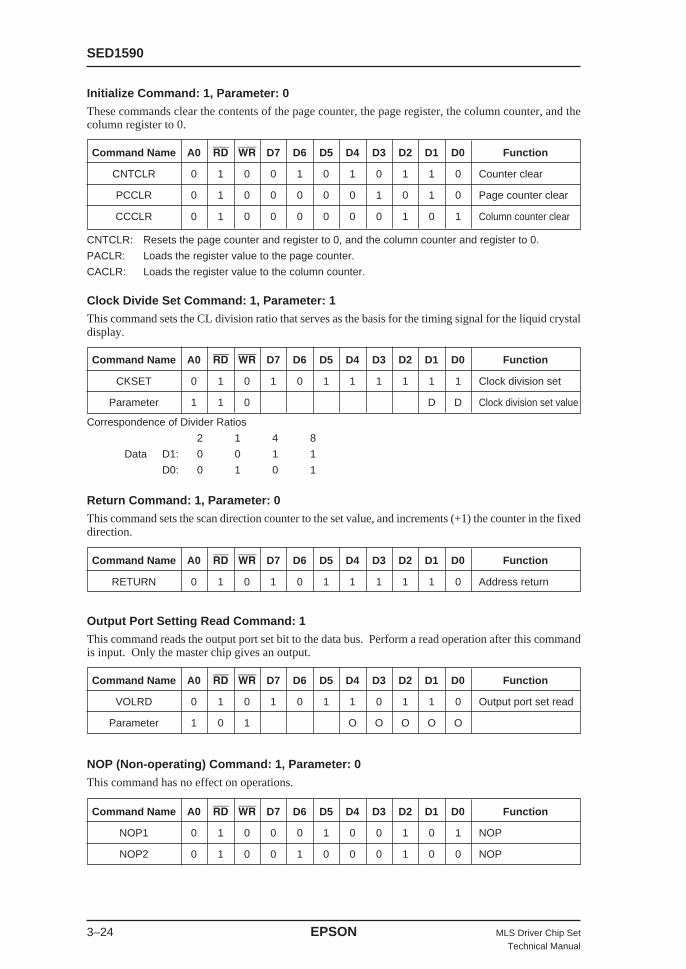
SED1590
3–24 EPSON MLS Driver Chip SetTechnical Manual
Initialize Command: 1, Parameter: 0
These commands clear the contents of the page counter, the page register, the column counter, and thecolumn register to 0.
Clock Divide Set Command: 1, Parameter: 1
This command sets the CL division ratio that serves as the basis for the timing signal for the liquid crystaldisplay.
Return Command: 1, Parameter: 0
This command sets the scan direction counter to the set value, and increments (+1) the counter in the fixeddirection.
Command Name A0 RD WR D7 D6 D5 D4 D3 D2 D1 D0 Function
CKSET 0 1 0 1 0 1 1 1 1 1 1 Clock division set
Parameter 1 1 0 D D Clock division set value
Correspondence of Divider Ratios
2 1 4 8
Data D1: 0 0 1 1
D0: 0 1 0 1
Command Name A0 RD WR D7 D6 D5 D4 D3 D2 D1 D0 Function
CNTCLR 0 1 0 0 1 0 1 0 1 1 0 Counter clear
PCCLR 0 1 0 0 0 0 0 1 0 1 0 Page counter clear
CCCLR 0 1 0 0 0 0 0 0 1 0 1 Column counter clear
CNTCLR: Resets the page counter and register to 0, and the column counter and register to 0.
PACLR: Loads the register value to the page counter.
CACLR: Loads the register value to the column counter.
Command Name A0 RD WR D7 D6 D5 D4 D3 D2 D1 D0 Function
RETURN 0 1 0 1 0 1 1 1 1 1 0 Address return
NOP (Non-operating) Command: 1, Parameter: 0
This command has no effect on operations.
Output Port Setting Read Command: 1
This command reads the output port set bit to the data bus. Perform a read operation after this commandis input. Only the master chip gives an output.
Command Name A0 RD WR D7 D6 D5 D4 D3 D2 D1 D0 Function
VOLRD 0 1 0 1 0 1 1 0 1 1 0 Output port set read
Parameter 1 0 1 O O O O O
Command Name A0 RD WR D7 D6 D5 D4 D3 D2 D1 D0 Function
NOP1 0 1 0 0 0 1 0 0 1 0 1 NOP
NOP2 0 1 0 0 1 0 0 0 1 0 0 NOP
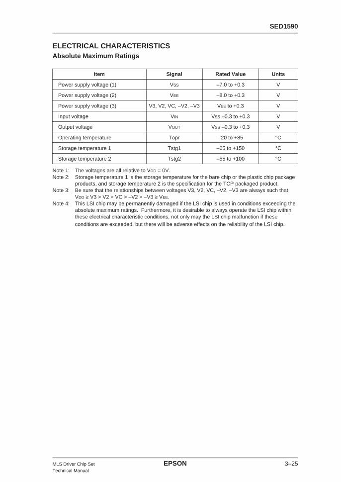
SED1590
MLS Driver Chip Set EPSON 3–25Technical Manual
ELECTRICAL CHARACTERISTICSAbsolute Maximum Ratings
Item Signal Rated Value Units
Power supply voltage (1) VSS –7.0 to +0.3 V
Power supply voltage (2) VEE –8.0 to +0.3 V
Power supply voltage (3) V3, V2, VC, –V2, –V3 VEE to +0.3 V
Input voltage VIN VSS –0.3 to +0.3 V
Output voltage VOUT VSS –0.3 to +0.3 V
Operating temperature Topr –20 to +85 °C
Storage temperature 1 Tstg1 –65 to +150 °C
Storage temperature 2 Tstg2 –55 to +100 °C
Note 1: The voltages are all relative to VDD = 0V.Note 2: Storage temperature 1 is the storage temperature for the bare chip or the plastic chip package
products, and storage temperature 2 is the specification for the TCP packaged product.Note 3: Be sure that the relationships between voltages V3, V2, VC, –V2, –V3 are always such that
VDD ≥ V3 > V2 > VC > –V2 > –V3 ≥ VEE.Note 4: This LSI chip may be permanently damaged if the LSI chip is used in conditions exceeding the
absolute maximum ratings. Furthermore, it is desirable to always operate the LSI chip withinthese electrical characteristic conditions, not only may the LSI chip malfunction if theseconditions are exceeded, but there will be adverse effects on the reliability of the LSI chip.

SED1590
3–26 EPSON MLS Driver Chip SetTechnical Manual
DC CharacteristicsUnless otherwise stated, VDD = V3 = 0V, VSS = –3.0V, VEE = –V3 = –6.0V, V2 = –1.5V, VC = –3.0, –V2 = –4.5V
Item Symbol Parameter Min Typ Max UnitsCorresponding
Terminal
Power supply voltage (1) VSS –3.6 –3.0 –2.7 V VSS
Power supply voltage (2) VEE –7.2 –6.0 –5.4 V VEE
Power supply voltage (3) V3 VDD V V3
Power supply voltage (4)V2
0.25V V2
VEE
Power supply voltage (5)VC
0.50V VC
VEE
Power supply voltage (6)–V2
0.75V –V2
VEE
Power supply voltage (7) –V3 VEE V –V3
High-level input voltage VIHC 0.3VSS — VDD V *1
Low-level input voltage VILC VSS — 0.7 VSS V *1
High-level output voltage VOH IOH = –0.6mA VDD–0.4 — VDD V *2
Low-level output voltage VOL IOL = +0.6mA VSS — VSS+0.4 V *2
Schmidt high-level inputVIHS 0.3VSS — VDD V RES
voltage
Schmidt low-level inputVILS VSS — 0.7VSS V RES
voltage
Input leakage current ILI VSS ≤VIN≤VDD — — 5.0 µA *3
Input/output leakageILI/O VIN=VDD, VSS — — 5.0 µA *4
current
VSS = –3.0V,VEE = –6.0V
V3 = 0V,Driver output
RONV2 = –1.5V
— 0.6 1.0 kΩ O1~resistance VC = –3.0V O160
–V2 = –4.5V–V3 = –6.0V,
∆ V = 0.5V
Static consumptionISSQ
VIN = VDD— — 5 µA VSS
current or VSS
Static consumptionIEEQ VEE = –6.0V — — 5 µA VEE
current
Dynamic consumptionISSOP1 MPU access *6 — 1.5 2.0 µA VSS
current
Dynamic consumptionISSOP2 MPU no access *6 — 90 130 µA VSS
current
Dynamic consumptionIEEOP VEE = –6.0V — 12 20 µA VEE
current
Input terminalCI — — 8 pF *3
capacitance
Input/output terminalCI/O — — 15 pF *4
capacitance
Output terminalCO — — 7 pF SLP
capacitance
Oscillator frequency Ifosc Ta = 25°C — 24 — kHz *5
Freq. = 1MHzTa = 25°CIC alone
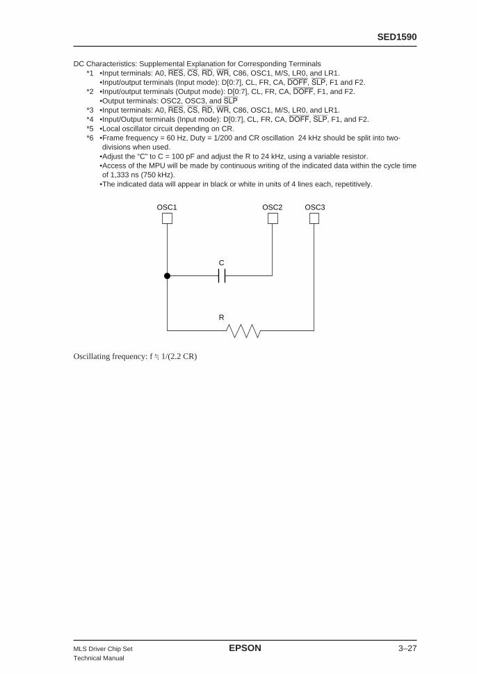
SED1590
MLS Driver Chip Set EPSON 3–27Technical Manual
DC Characteristics: Supplemental Explanation for Corresponding Terminals*1 •Input terminals: A0, RES, CS, RD, WR, C86, OSC1, M/S, LR0, and LR1.
•Input/output terminals (Input mode): D[0:7], CL, FR, CA, DOFF, SLP, F1 and F2.*2 •Input/output terminals (Output mode): D[0:7], CL, FR, CA, DOFF, F1, and F2.
•Output terminals: OSC2, OSC3, and SLP*3 •Input terminals: A0, RES, CS, RD, WR, C86, OSC1, M/S, LR0, and LR1.*4 •Input/Output terminals (Input mode): D[0:7], CL, FR, CA, DOFF, SLP, F1, and F2.*5 •Local oscillator circuit depending on CR.*6 •Frame frequency = 60 Hz, Duty = 1/200 and CR oscillation 24 kHz should be split into two-
divisions when used.•Adjust the “C” to C = 100 pF and adjust the R to 24 kHz, using a variable resistor.•Access of the MPU will be made by continuous writing of the indicated data within the cycle timeof 1,333 ns (750 kHz).
•The indicated data will appear in black or white in units of 4 lines each, repetitively.
Oscillating frequency: f .=. 1/(2.2 CR)
C
OSC1 OSC2 OSC3
R
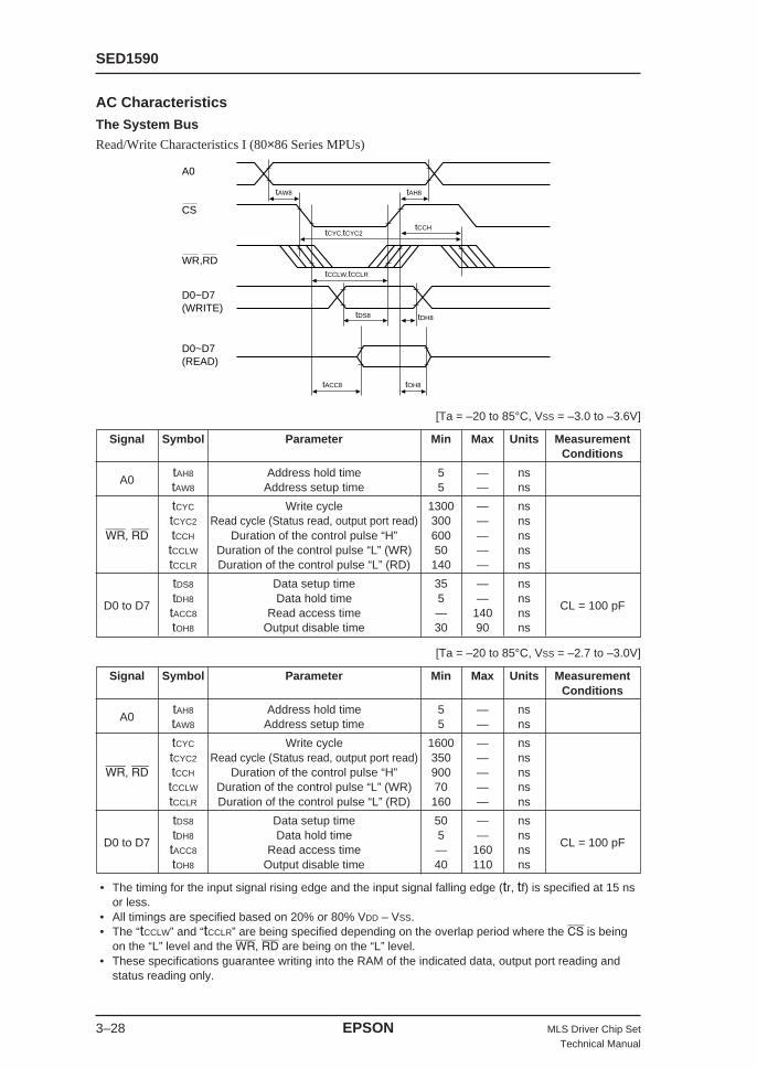
SED1590
3–28 EPSON MLS Driver Chip SetTechnical Manual
AC CharacteristicsThe System Bus
Read/Write Characteristics I (80×86 Series MPUs)
A0
CS
WR,RD
tAW8 tAH8
tCCHtCYC,tCYC2
tCCLW,tCCLR
tDS8 tDH8
tOH8tACC8
D0~D7(WRITE)
D0~D7(READ)
[Ta = –20 to 85°C, VSS = –3.0 to –3.6V]
Signal Symbol Parameter Min Max Units MeasurementConditions
A0tAH8 Address hold time 5 — nstAW8 Address setup time 5 — ns
tCYC Write cycle 1300 — nstCYC2 Read cycle (Status read, output port read) 300 — ns
WR, RD tCCH Duration of the control pulse “H” 600 — nstCCLW Duration of the control pulse “L” (WR) 50 — nstCCLR Duration of the control pulse “L” (RD) 140 — ns
tDS8 Data setup time 35 — ns
D0 to D7tDH8 Data hold time 5 — ns
CL = 100 pFtACC8 Read access time — 140 nstOH8 Output disable time 30 90 ns
[Ta = –20 to 85°C, VSS = –2.7 to –3.0V]
Signal Symbol Parameter Min Max Units MeasurementConditions
A0tAH8 Address hold time 5 — nstAW8 Address setup time 5 — ns
tCYC Write cycle 1600 — nstCYC2 Read cycle (Status read, output port read) 350 — ns
WR, RD tCCH Duration of the control pulse “H” 900 — nstCCLW Duration of the control pulse “L” (WR) 70 — nstCCLR Duration of the control pulse “L” (RD) 160 — ns
tDS8 Data setup time 50 — ns
D0 to D7tDH8 Data hold time 5 — ns
CL = 100 pFtACC8 Read access time — 160 nstOH8 Output disable time 40 110 ns
• The timing for the input signal rising edge and the input signal falling edge (tr, tf) is specified at 15 nsor less.
• All timings are specified based on 20% or 80% VDD – VSS.• The “tCCLW” and “tCCLR” are being specified depending on the overlap period where the CS is being
on the “L” level and the WR, RD are being on the “L” level.• These specifications guarantee writing into the RAM of the indicated data, output port reading and
status reading only.
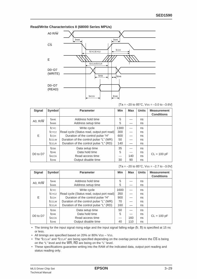
SED1590
MLS Driver Chip Set EPSON 3–29Technical Manual
Read/Write Characteristics II (68000 Series MPUs)
A0 R/W
CS
E
tAW6 tAH6
tCCHtCYC,tCYC2
tCCLW,tCCLR
tDS6 tDH6
tOH6tACC6
D0~D7(WRITE)
D0~D7(READ)
[Ta = –20 to 85°C, VSS = –3.0 to –3.6V]
Signal Symbol Parameter Min Max Units MeasurementConditions
A0, R/W tAH6 Address hold time 5 — nstAW6 Address setup time 5 — ns
tCYC Write cycle 1300 — nstCYC2 Read cycle (Status read, output port read) 300 — ns
E tCCH Duration of the control pulse “H” 600 — nstCCLW Duration of the control pulse “L” (WR) 50 — nstCCLR Duration of the control pulse “L” (RD) 140 — ns
tDS6 Data setup time 35 — ns
D0 to D7tDH6 Data hold time 5 — ns
CL = 100 pFtACC6 Read access time — 140 nstOH6 Output disable time 30 90 ns
[Ta = –20 to 85°C, VSS = –2.7 to –3.0V]
Signal Symbol Parameter Min Max Units MeasurementConditions
A0, R/W tAH6 Address hold time 5 — nstAW6 Address setup time 5 — ns
tCYC Write cycle 1600 — nstCYC2 Read cycle (Status read, output port read) 350 — ns
E tCCH Duration of the control pulse “H” 900 — nstCCLW Duration of the control pulse “L” (WR) 70 — nstCCLR Duration of the control pulse “L” (RD) 160 — ns
tDS6 Data setup time 50 — ns
D0 to D7tDH6 Data hold time 5 — ns
CL = 100 pFtACC6 Read access time — 160 nstOH6 Output disable time 40 110 ns
• The timing for the input signal rising edge and the input signal falling edge (tr, tf) is specified at 15 nsor less.
• All timings are specified based on 20% or 80% VDD – VSS.• The “tCCLW” and “tCCLR” are being specified depending on the overlap period where the CS is being
on the “L” level and the WR, RD are being on the “L” level.• These specifications guarantee writing into the RAM of the indicated data, output port reading and
status reading only.
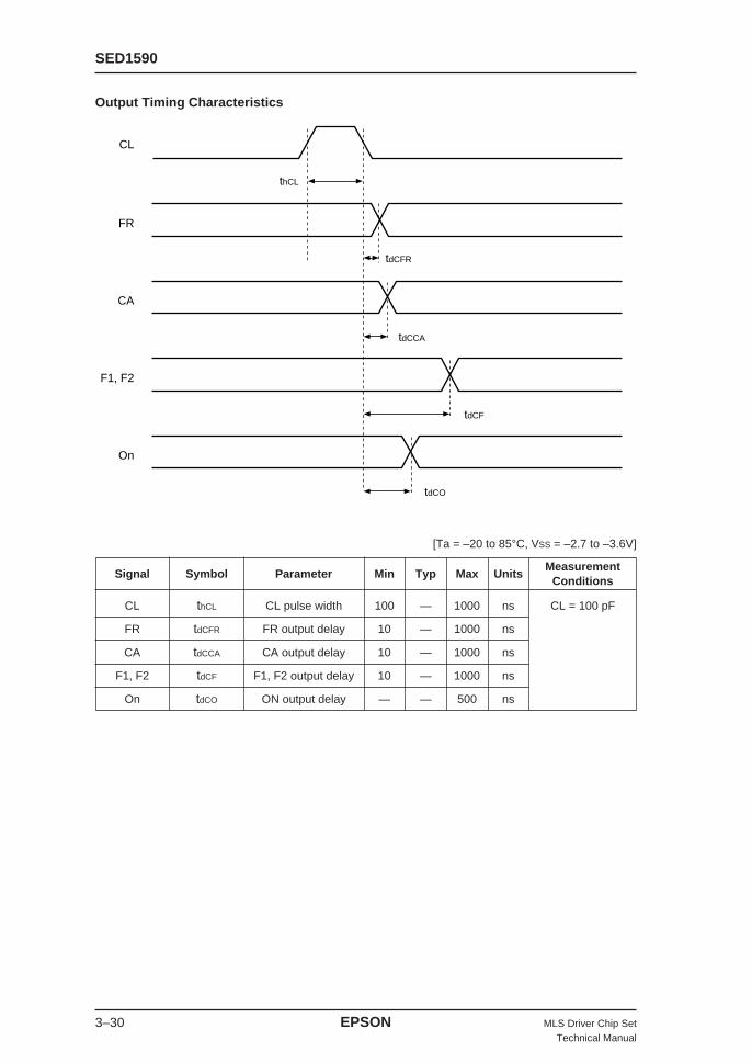
SED1590
3–30 EPSON MLS Driver Chip SetTechnical Manual
Output Timing Characteristics
CL
FR
CA
F1, F2
On
tdCFR
tdCCA
tdCO
tdCF
thCL
[Ta = –20 to 85°C, VSS = –2.7 to –3.6V]
Signal Symbol Parameter Min Typ Max UnitsMeasurement
Conditions
CL thCL CL pulse width 100 — 1000 ns CL = 100 pF
FR tdCFR FR output delay 10 — 1000 ns
CA tdCCA CA output delay 10 — 1000 ns
F1, F2 tdCF F1, F2 output delay 10 — 1000 ns
On tdCO ON output delay — — 500 ns
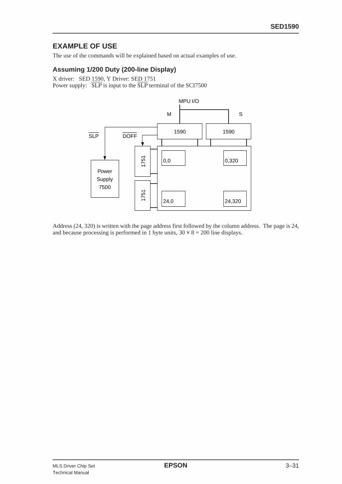
SED1590
MLS Driver Chip Set EPSON 3–31Technical Manual
EXAMPLE OF USEThe use of the commands will be explained based on actual examples of use.
Assuming 1/200 Duty (200-line Display)X driver: SED 1590, Y Driver: SED 1751Power supply: SLP is input to the SLP terminal of the SCI7500
Address (24, 320) is written with the page address first followed by the column address. The page is 24,and because processing is performed in 1 byte units, 30 × 8 = 200 line displays.
0,0
1590
1751
1751
1590
24,0
0,320
24,320
Power
Supply
7500
SLP DOFF
M
MPU I/O
S

SED1590
3–32 EPSON MLS Driver Chip SetTechnical Manual
Example of Actual UseThe Power-up Process
Turn on the system power supply (VCC).↓
Do not neglect the power-on reset.At the time of reset the default values will be as follows:
Sleep status: Sleep statusDON/DOFF status: DOFF Status(The divider OFF has not been applied.)Display normal/reversed: NormalDuty: 1/240 (set to 240 lines)Non-display interval: 0 selected intervalsFR period: Each 11 selected intervalsPage address register: 00.HColumn address register: 000.HPage address direction: Forward directionColumn address direction: IncrementScanning direction: Column directionMLS pattern: Changes at each 8 selected intervalsPower supply control bit: 00.HClock 2 divider: 0.H
↓Input commands for the settings to be changed
Example: Change the dutyReverse the scan directionSet the scaning direction to the page directionSet the non-display interval
↓Sleep off
↓Display Data input
Example: Write StartWrite data input
↓ 1 line’s worthReturn command
Repeat for the number of lines to be displayed.↓
Display ON (at least 40 ms after the sleep was released).↓
Rewrite only a portion of the display contents.Example: Page address set
Column address setWrite startWrite data input
↓ The amount to be rewrittenReturn command
Repeat for the number of lines to be displayed.↓
Read the part where there is content displayed.Example: Page address set
Column address setRead startData read
↓ The amount to be read Return commandRepeat for the number of lines to be displayed.
↓
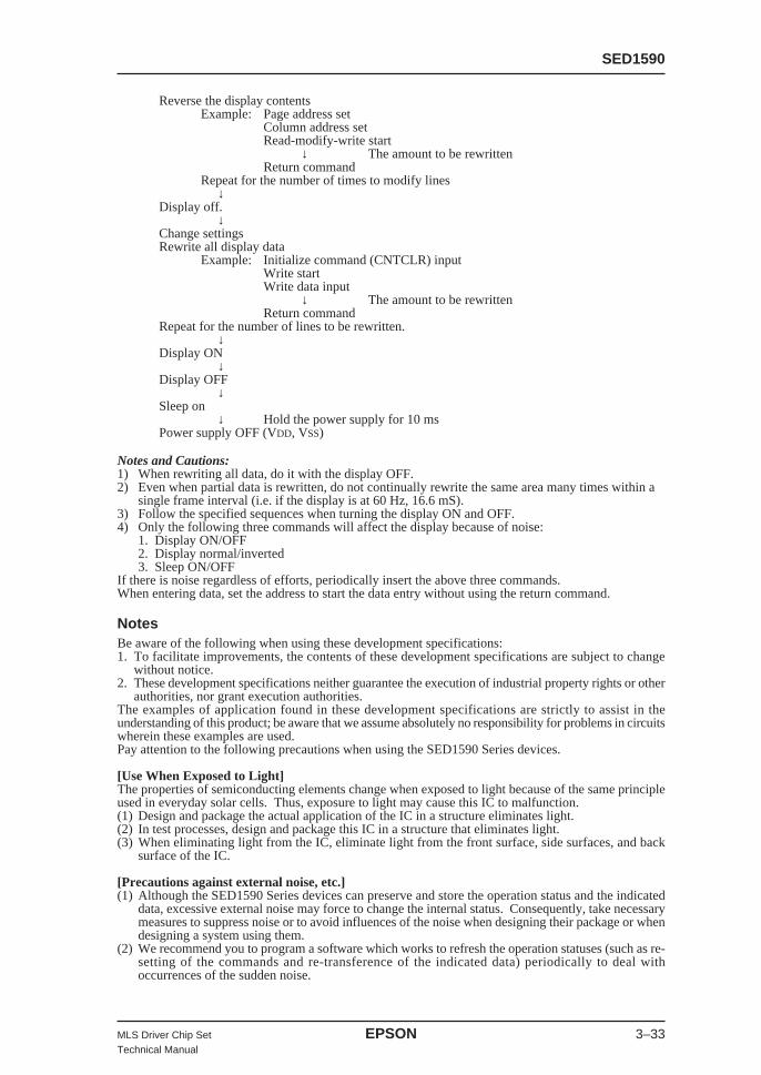
SED1590
MLS Driver Chip Set EPSON 3–33Technical Manual
Reverse the display contentsExample: Page address set
Column address setRead-modify-write start
↓ The amount to be rewrittenReturn command
Repeat for the number of times to modify lines↓
Display off.↓
Change settingsRewrite all display data
Example: Initialize command (CNTCLR) inputWrite startWrite data input
↓ The amount to be rewrittenReturn command
Repeat for the number of lines to be rewritten.↓
Display ON↓
Display OFF↓
Sleep on↓ Hold the power supply for 10 ms
Power supply OFF (VDD, VSS)
Notes and Cautions:1) When rewriting all data, do it with the display OFF.2) Even when partial data is rewritten, do not continually rewrite the same area many times within a
single frame interval (i.e. if the display is at 60 Hz, 16.6 mS).3) Follow the specified sequences when turning the display ON and OFF.4) Only the following three commands will affect the display because of noise:
1. Display ON/OFF2. Display normal/inverted3. Sleep ON/OFF
If there is noise regardless of efforts, periodically insert the above three commands.When entering data, set the address to start the data entry without using the return command.
NotesBe aware of the following when using these development specifications:1. To facilitate improvements, the contents of these development specifications are subject to change
without notice.2. These development specifications neither guarantee the execution of industrial property rights or other
authorities, nor grant execution authorities.The examples of application found in these development specifications are strictly to assist in theunderstanding of this product; be aware that we assume absolutely no responsibility for problems in circuitswherein these examples are used.Pay attention to the following precautions when using the SED1590 Series devices.
[Use When Exposed to Light]The properties of semiconducting elements change when exposed to light because of the same principleused in everyday solar cells. Thus, exposure to light may cause this IC to malfunction.(1) Design and package the actual application of the IC in a structure eliminates light.(2) In test processes, design and package this IC in a structure that eliminates light.(3) When eliminating light from the IC, eliminate light from the front surface, side surfaces, and back
surface of the IC.
[Precautions against external noise, etc.](1) Although the SED1590 Series devices can preserve and store the operation status and the indicated
data, excessive external noise may force to change the internal status. Consequently, take necessarymeasures to suppress noise or to avoid influences of the noise when designing their package or whendesigning a system using them.
(2) We recommend you to program a software which works to refresh the operation statuses (such as re-setting of the commands and re-transference of the indicated data) periodically to deal withoccurrences of the sudden noise.
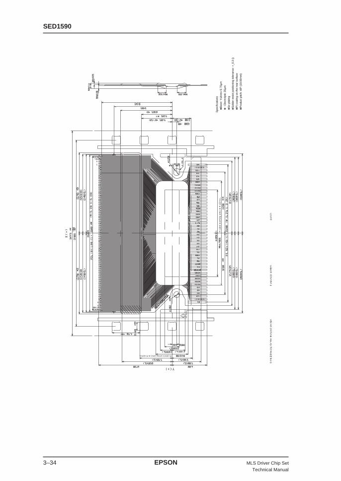
SED1590
3–34 EPSON MLS Driver Chip SetTechnical Manual
(Molded marking area) * Mold No.
Molded marking area * Mold No.
Detail drawing for the test pad section
Output pin pattern
punch
Spe
cific
atio
ns
B
ase:
Yub
irex-
S 7
5µm
:
Ele
ctro
lytic
35µ
m
S
n pl
atin
g
S
olde
r re
sist
pos
ition
ing
tole
ranc
e: +
_0.3
()
P
I coa
ting
on th
e re
ar s
urfa
ce
P
rodu
ct p
itch:
4IP
(19
.00m
m)

SED1750

SED1750
MLS Driver Chip Set EPSON iTechnical Manual
Contents
OVERVIEW ................................................................................................................................... 4-1
TERMINAL FUNCTIONS .............................................................................................................. 4-7
ABSOLUTE MAXIMUM RATINGS.............................................................................................. 4-11

SED1750
MLS Driver Chip Set EPSON 4–1Technical Manual
OVERVIEWThe SED1750 is an MLS (Multi Line Selection) driving, 160 output, triple-value low resistance common(low) driver which can realize high picture quality and high speed responses.Receiving signals from an LCD controller such as the SED1335 or SED1351, it works to make 4-line MLSdrives in combination with the SED1580 or in combination with the SED1590 receiving signals direct fromthe MPU. Employing the SCI7500 as the power IC, the power to use for the MLS drive liquid crystaldisplay system can be prepared easily.Adopting a slim chip shape which is more advantageous to realize narrower borders with the LCD panels,the SED1750 is capable of making low voltage logic power operations and is applicable to a wide rangeof applications.Owing to its pad layout designed to facilitate its installation to the substrate and thanks to its two-waychoices of the driver output sequence, the highest working efficiency can be acquired with a 1/160 or 1/320 duty panel.
Features• LCD driver outputs ...................................... 160• Low output ON resistance• High duty drive supported ........................... 1/320 (Reference value)• Broad range of LC drive voltages ............... + 14 to + 42 V (VCC = 2.7 to 5.5 V)• Output shift direction pin select is possible• Can be switched between 140 and 160 outputs• Non-biased display OFF function• Logic system power source ......................... 2.7 V to 5.5 V• LC power source offset bias can be adjusted relative to the VDDH and GND levels• Slim chip shape• D0B .............................................................. Au Bump die• T0A ............................................................... TCP
Pad Layout
YDie.No.
X
179
1
180
203
68
43
67
44
Chip size 15.62 mm × 2.47 mmPad pitch 80 µm (Min.)Chip thickness 525 µm ± 25 µm
1) Au Bump Specifications (SED1750DOB) Reference Values OnlyAu vertical bump
Parallel to Scribe × Perpendicular to Scribe ± ToleranceBump Size A 60 µm × 75 µm ± 4 mm (Pad No. 1 to 43, 68 to 179)Bump Size B 80 µm × 50 µm ± 4 mm (Pad No. 44 to 67, 180 to 203)Bump height 17 to 28 µm (The details specified in the acceptance specifications.)
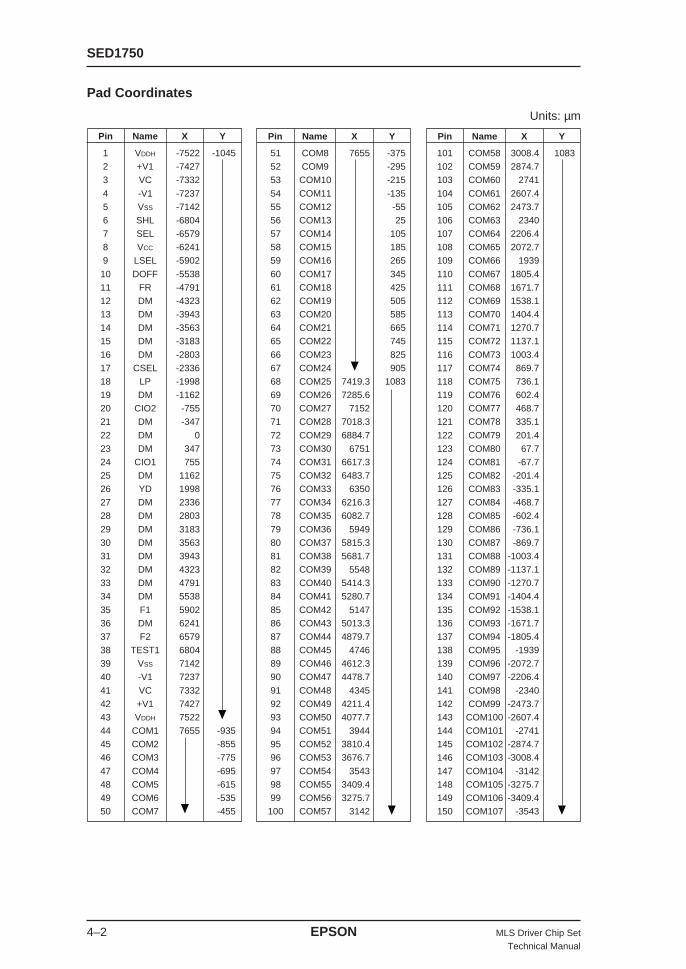
SED1750
4–2 EPSON MLS Driver Chip SetTechnical Manual
Units: µm
Pad Coordinates
51 COM8 7655 -37552 COM9 -29553 COM10 -215
54 COM11 -13555 COM12 -5556 COM13 2557 COM14 10558 COM15 18559 COM16 265
60 COM17 34561 COM18 42562 COM19 50563 COM20 58564 COM21 66565 COM22 745
66 COM23 82567 COM24 90568 COM25 7419.3 108369 COM26 7285.670 COM27 715271 COM28 7018.3
72 COM29 6884.773 COM30 675174 COM31 6617.375 COM32 6483.776 COM33 635077 COM34 6216.378 COM35 6082.7
79 COM36 594980 COM37 5815.381 COM38 5681.782 COM39 554883 COM40 5414.384 COM41 5280.7
85 COM42 514786 COM43 5013.387 COM44 4879.788 COM45 474689 COM46 4612.390 COM47 4478.7
91 COM48 434592 COM49 4211.493 COM50 4077.794 COM51 394495 COM52 3810.496 COM53 3676.7
97 COM54 354398 COM55 3409.499 COM56 3275.7
100 COM57 3142
Pin Name X Y
101 COM58 3008.4 1083102 COM59 2874.7103 COM60 2741
104 COM61 2607.4105 COM62 2473.7106 COM63 2340107 COM64 2206.4108 COM65 2072.7109 COM66 1939
110 COM67 1805.4111 COM68 1671.7112 COM69 1538.1113 COM70 1404.4114 COM71 1270.7115 COM72 1137.1
116 COM73 1003.4117 COM74 869.7118 COM75 736.1119 COM76 602.4120 COM77 468.7121 COM78 335.1
122 COM79 201.4123 COM80 67.7124 COM81 -67.7125 COM82 -201.4126 COM83 -335.1127 COM84 -468.7128 COM85 -602.4
129 COM86 -736.1130 COM87 -869.7131 COM88 -1003.4132 COM89 -1137.1133 COM90 -1270.7134 COM91 -1404.4
135 COM92 -1538.1136 COM93 -1671.7137 COM94 -1805.4138 COM95 -1939139 COM96 -2072.7140 COM97 -2206.4
141 COM98 -2340142 COM99 -2473.7143 COM100 -2607.4144 COM101 -2741145 COM102 -2874.7146 COM103 -3008.4
147 COM104 -3142148 COM105 -3275.7149 COM106 -3409.4150 COM107 -3543
Pin Name X YPin Name X Y
1 VDDH -7522 -10452 +V1 -74273 VC -7332
4 -V1 -72375 VSS -71426 SHL -68047 SEL -65798 VCC -62419 LSEL -5902
10 DOFF -553811 FR -479112 DM -432313 DM -394314 DM -356315 DM -3183
16 DM -280317 CSEL -233618 LP -199819 DM -116220 CIO2 -75521 DM -347
22 DM 023 DM 34724 CIO1 75525 DM 116226 YD 199827 DM 233628 DM 2803
29 DM 318330 DM 356331 DM 394332 DM 432333 DM 479134 DM 5538
35 F1 590236 DM 624137 F2 657938 TEST1 680439 VSS 714240 -V1 7237
41 VC 733242 +V1 742743 VDDH 752244 COM1 7655 -93545 COM2 -85546 COM3 -775
47 COM4 -69548 COM5 -61549 COM6 -53550 COM7 -455

SED1750
MLS Driver Chip Set EPSON 4–3Technical Manual
169 COM126 -6082.7 1083170 COM127 -6216.3
171 COM128 -6350172 COM129 -6483.7173 COM130 -6617.3174 COM131 -6751175 COM132 -6884.7176 COM133 -7018.3
177 COM134 -7152178 COM135 -7285.6179 COM136 -7419.3180 COM137 -7655 905181 COM138 825182 COM139 745
183 COM140 665184 COM141 585185 COM142 505186 COM143 425
Pin Name X Y
187 COM144 -7655 345188 COM145 265
189 COM146 185190 COM147 105191 COM148 25192 COM149 -55193 COM150 -135194 COM151 -215
195 COM152 -295196 COM153 -375197 COM154 -455198 COM155 -535199 COM156 -615200 COM157 -695
201 COM158 -775202 COM159 -855203 COM160 -935
Pin Name X YPin Name X Y
151 COM108 -3676.7 1083152 COM109 -3810.4
153 COM110 -3944154 COM111 -4077.7155 COM112 -4211.4156 COM113 -4345157 COM114 -4478.7158 COM115 -4612.3
159 COM116 -4746160 COM117 -4879.7161 COM118 -5013.3162 COM119 -5147163 COM120 -5280.7164 COM121 -5414.3
165 COM122 -5548166 COM123 -5681.7167 COM124 -5815.3168 COM125 -5949
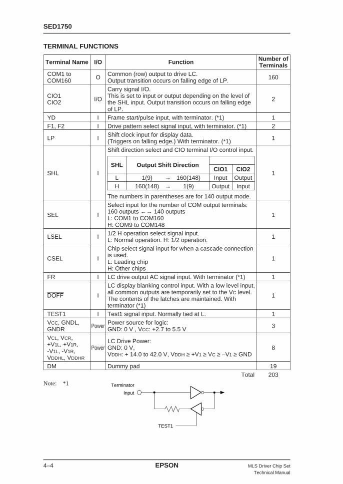
SED1750
4–4 EPSON MLS Driver Chip SetTechnical Manual
TERMINAL FUNCTIONS
Input
Terminator
TEST1
Terminal Name I/O Function Number ofTerminals
COM1 to O Common (row) output to drive LC. 160COM160 Output transition occurs on falling edge of LP.Carry signal I/O.
CIO1 I/O This is set to input or output depending on the level of 2CIO2 the SHL input. Output transition occurs on falling edgeof LP.
YD I Frame start/pulse input, with terminator. (*1) 1F1, F2 I Drive pattern select signal input, with terminator. (*1) 2
LP I Shift clock input for display data. 1(Triggers on falling edge.) With terminator. (*1)Shift direction select and CIO terminal I/O control input.
SHL I 1
The numbers in parentheses are for 140 output mode.Select input for the number of COM output terminals:
SEL I 160 outputs ←→ 140 outputs 1L: COM1 to COM160H: COM9 to COM148
LSEL I 1/2 H operation select signal input. 1L: Normal operation. H: 1/2 operation.Chip select signal input for when a cascade connection
CSEL I is used. 1L: Leading chipH: Other chips
FR I LC drive output AC signal input. With terminator (*1) 1LC display blanking control input. With a low level input,
DOFF I all common outputs are temporarily set to the VC level. 1The contents of the latches are maintained. Withterminator (*1)
TEST1 I Test1 signal input. Normally tied at L. 1VCC, GNDL, Power Power source for logic: 3GNDR GND: 0 V , VCC: +2.7 to 5.5 VVCL, VCR, LC Drive Power:+V1L, +V1R, Power GND: 0 V, 8-V1L, -V1R, VDDH: + 14.0 to 42.0 V, VDDH ≥ +V1 ≥ VC ≥ –V1 ≥ GNDVDDHL, VDDHR
DM Dummy pad 19Total 203
Note: *1
SHL Output Shift DirectionCIO1 CIO2
L 1(9) → 160(148) Input OutputH 160(148) → 1(9) Output Input
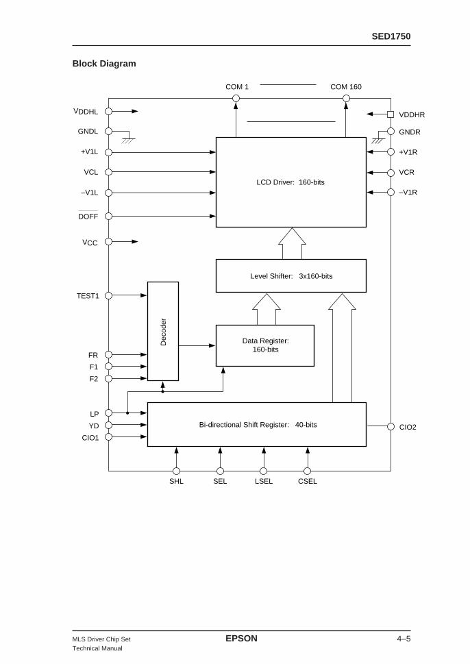
SED1750
MLS Driver Chip Set EPSON 4–5Technical Manual
Block Diagram
VDDHL
GNDL
+V1L
VCL
–V1L
DOFF
VDDHR
GNDR
+V1R
VCR
–V1R
CIO2
LCD Driver: 160-bits
Level Shifter: 3x160-bits
Dec
oder
Bi-directional Shift Register: 40-bits
Data Register:160-bits
VCC
TEST1
LP
YD
CIO1
COM 1 COM 160
SHL SEL LSEL CSEL
FR
F1
F2
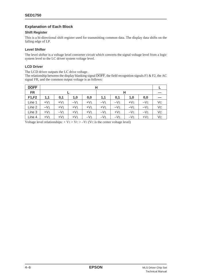
SED1750
4–6 EPSON MLS Driver Chip SetTechnical Manual
Explanation of Each BlockShift Register
This is a bi-directional shift register used for transmitting common data. The display data shifts on thefalling edge of LP.
Level Shifter
The level shifter is a voltage level converter circuit which converts the signal voltage level from a logicsystem level to the LC driver system voltage level.
LCD Driver
The LCD driver outputs the LC drive voltage.The relationship between the display blanking signal DOFF, the field recognition signals F1 & F2, the ACsignal FR, and the common output voltage is as follows:
DOFF H LFR L H —
F1,F2 1,1 0,1 1,0 0,0 1,1 0,1 1,0 0,0 —Line 1 +V1 +V1 –V1 +V1 –V1 –V1 +V1 –V1 VC
Line 2 –V1 +V1 +V1 +V1 +V1 –V1 –V1 –V1 VC
Line 3 +V1 –V1 +V1 +V1 –V1 +V1 –V1 –V1 VC
Line 4 +V1 +V1 +V1 –V1 –V1 –V1 –V1 +V1 VC
Voltage level relationships: + V1 > VC > –V1 (VC is the center voltage level)
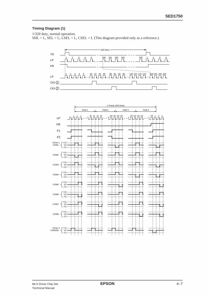
SED1750
MLS Driver Chip Set EPSON 4–7Technical Manual
Timing Diagram (1)
1/320 duty, normal operation.SHL = L, SEL = L, LSEL = L, CSEL = L (This diagram provided only as a reference.)
+V1VC
–V1
F2
F1
FR
LP
Driver 1COM1
+V1VC
–V1COM2
+V1VC
–V1COM3
+V1VC
–V1COM4
+V1VC
–V1COM5
+V1VC
–V1COM6
+V1VC
–V1COM7
+V1VC
–V1COM8
+V1VC
–V1
Driver 2COM160
Field 1 Field 2 Field 3
1 Frame (320 lines)
Field 4
1 2 3 80 81 82 83 160 161 162 163 240 241 242 243 320 1 2 3
1
1 2 3 4 5 40 41 42 43 80 81 82 83 120 121 122 123 160 161 162 163
2 3 4 5
320 lines
160 161 162 163 320 1 2 3 4YD
LP
FR
LP
CIO 1
CIO 2

SED1750
4–8 EPSON MLS Driver Chip SetTechnical Manual
Timing Diagram (2)
1/320 duty, 1/2 H operation.SHL = L, SEL = L, LSEL = H, CSEL = L (This diagram provided only as a reference.)
+V1VC
–V1
F2
F1
FR
LP
Driver 1COM1
+V1VC
–V1COM2
+V1VC
–V1COM3
+V1VC
–V1COM4
+V1VC
–V1COM5
+V1VC
–V1COM6
+V1VC
–V1COM7
+V1VC
–V1COM8
+V1VC
–V1
Driver 2COM160
Field 1 Field 2 Field 3
1 Frame (320 lines)
Field 4
2/320 2/1 2/80 2/81 2/160 2/161 2/240 2/241 2/320 2/1
1/1 1/2 1/81 1/82 1/161 1/162 1/241 1/242 1/1 1/2
1/1
1/1
2/1
1/2
2/2
1/3 1/40
2/40
1/41
2/41
1/80
2/80
1/81
2/81
1/120
2/120
1/121
2/121
1/160
2/160
1/161
2/161
2/1 1/2 2/2 1/3
320 lines
1/160 2/161 1/162 2/163 2/320 1/1 2/1 1/2 2/2YD
LP
FR
LP
CIO
CIO
1
2

SED1750
MLS Driver Chip Set EPSON 4–9Technical Manual
ABSOLUTE MAXIMUM RATINGS
Item Signal Rated Value UnitsPower voltage (1) VCC –0.3 to +7.0 VPower voltage (2) VDDH –0.3 to + 45.0 VPower voltage (3) ± V1, VC GND – 0.3 to VDDH + 0.3 VInput voltage VI GND – 0.3 to VCC + 0.3 VOutput voltage VO GND – 0.3 to VCC + 0.3 VCIO output current IO1 20 mAOperating temperature Topr –30 to +85 °CStorage temperature 1 Tstg1 –65 to +150 °CStorage temperature 2 Tstg2 –55 to +100 °C
NOTE 1: The voltages are all relative to GND = 0 V.NOTE 2: Storage temperature 1 is for the chip alone, and storage temperature 2 is for the TCP
product.NOTE 3: Ensure that the relationship between +V1, VC, and –V1 is always as follows:
VDDH ≥ +V1 ≥ VC ≥ –V1 ≥ GND.
NOTE 4: The LSI may be permanently damaged if the logic system power is floating or VCC is lessthan or equal to 2.6 V when power is applied to the LC drive system. Special caution mustbe paid to the power sequences during power up and power down.
VCC
GND (–V1)
VDDH/2 (VC)
VDDH (+V1)
Logic System LCD System

SED1750
4–10 EPSON MLS Driver Chip SetTechnical Manual
Electrical CharacteristicsDC Characteristics
Unless otherwise noted, GND = 0 V, VCC = + 5.0 V ± 10%, Ta = –30 to 85°C
Item Signal ParameterApplicable
Min Typ Max UnitTerminals
Power Supply VCC VCC 2.7 5.0 5.5 VVoltage (1)
Range Operating VDDH Function VDDH 8.0 42.0 VVoltages
Power Supply +V1 Recommended Value +V1 VDDH VVoltage (2)
Power SupplyVC Recommended Value VC VDDH/2 VVoltage (3)
Power Supply –V1 Recommended Value –V1 GND VVoltage (4)
High-level Input VIH 0.8VCC VVoltage
VCC = 2.7 to 5.5VLow-level Input VIL 0.2VCC VVoltage
High-level OutputVOH
IOH =VCC–0.4 VVoltage
VCC = 2.7 to 5.5V –0.3mA
CIO1,CIO2Low-level Output VOL
IOL = 0.4 VVoltage 0.3mA
Input Leakage Current ILI GND ≤ VIN ≤ VCC 2.0 µA
Input/Output LeakageILI/O GND ≤ VIN ≤ VCC CIO1,CIO2 5.0 µACurrent
Static Current IGNDVDDH = 14.0~42.0V GND 25 µAVIH = VCC, VIL = GND
∆VON = 0.5 VVDDH = 0.55 0.7
Output Resistance RCOM Recommended +30.0V COM1 to
kΩparameter VDDH = COM120
0.5 0.7 +40.0V
VCC = +5.0 V, VIH = VCC
VIL = GND, fLP = 22.4 kHz 12 25Average Operating fFR = 70 Hz,Consumption Current ICC Input data: 1/320 No load VCC µA(1) VCC = 3.0 V
All other parameters 8 17the same as VCC = 5.0 V.
VDDH = +V1 = +30.0 V,Average Operating VC = VDDH/2, –V1 = 0.0 V,Consumption Current IDDH VCC = 5.0 V VDDH 7 13 µA(2) All other parameters
the same as the ICC item.
Input TerminalCI Freq. = 1 MHz 10 pFCapacity
Chip aloneInput/Output Terminal
CI/O Ta = 25°C CIO1,CIO2 18 pFCapacity
CIO1,CIO2,FR,YD,LP,SHL,SEL,
LSEL,CSEL,DOFF,F1,F2,
TEST1
LP,YD,SHL,SEL,LSEL,CSEL,F1,
F2,DOFF,TEST1,FR
LP,YD,SHL,SEL,LSEL,CSEL,F1,F2,DOFF,TEST1,FR
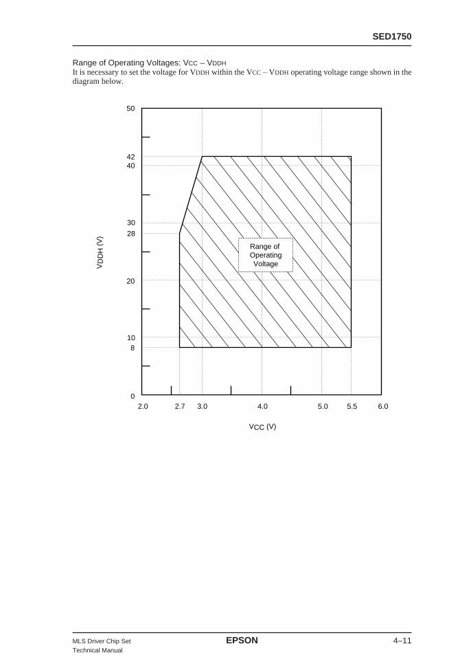
SED1750
MLS Driver Chip Set EPSON 4–11Technical Manual
Range of Operating Voltages: VCC – VDDHIt is necessary to set the voltage for VDDH within the VCC – VDDH operating voltage range shown in thediagram below.
Range of OperatingVoltage
50
4240
30
20
10
28
8
02.0 3.02.7 4.0
VCC (V)
VD
DH
(V
)
5.0 6.05.5
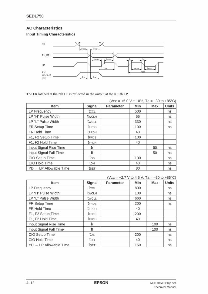
SED1750
4–12 EPSON MLS Driver Chip SetTechnical Manual
AC CharacteristicsInput Timing Characteristics
The FR latched at the nth LP is reflected in the output at the n+1th LP.
tDS tDH
tSET tWCLH tWCLL
tCCL
tFFDS tFFDH tr tf
tFRDS tFRDH
FR
F1, F2
LP
YDCIO1, 2(IN)
(VCC = +5.0 V ± 10%, Ta = –30 to +85°C)Item Signal Parameter Min Max Units
LP Frequency tCCL 500 nsLP “H” Pulse Width tWCLH 55 nsLP “L” Pulse Width tWCLL 330 nsFR Setup Time tFRDS 100 nsFR Hold Time tFRDH 40F1, F2 Setup Time tFFDS 100F1, F2 Hold Time tFFDH 40Input Signal Rise Time tr 50 nsInput Signal Fall Time tf 50 nsCIO Setup Time tDS 100 nsCIO Hold Time tDH 40 nsYD → LP Allowable Time tSET 80 ns
(VCC = +2.7 V to 4.5 V, Ta = –30 to +85°C)Item Signal Parameter Min Max Units
LP Frequency tCCL 800 nsLP “H” Pulse Width tWCLH 100 nsLP “L” Pulse Width tWCLL 660 nsFR Setup Time tFRDS 200 nsFR Hold Time tFRDH 40F1, F2 Setup Time tFFDS 200F1, F2 Hold Time tFFDH 40Input Signal Rise Time tr 100 nsInput Signal Fall Time tf 100 nsCIO Setup Time tDS 200 nsCIO Hold Time tDH 40 nsYD → LP Allowable Time tSET 150 ns
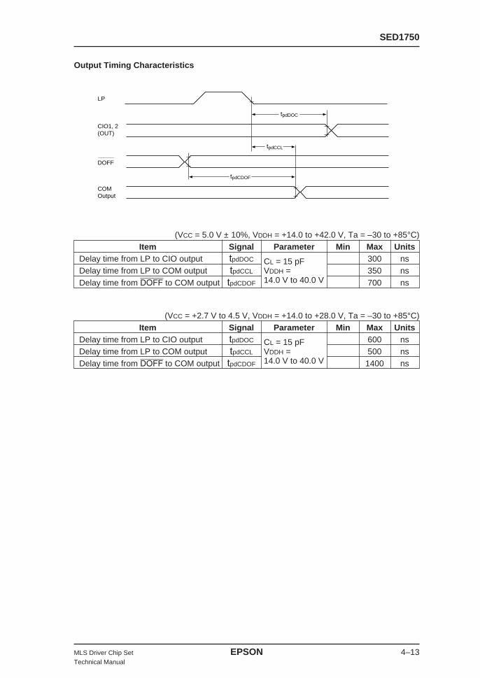
SED1750
MLS Driver Chip Set EPSON 4–13Technical Manual
Output Timing Characteristics
tpdCDOF
tpdCCL
tpdDOC
LP
DOFF
COMOutput
CIO1, 2(OUT)
(VCC = 5.0 V ± 10%, VDDH = +14.0 to +42.0 V, Ta = –30 to +85°C)Item Signal Parameter Min Max Units
Delay time from LP to CIO output tpdDOC CL = 15 pF 300 nsDelay time from LP to COM output tpdCCL VDDH = 350 nsDelay time from DOFF to COM output tpdCDOF 14.0 V to 40.0 V 700 ns
(VCC = +2.7 V to 4.5 V, VDDH = +14.0 to +28.0 V, Ta = –30 to +85°C)Item Signal Parameter Min Max Units
Delay time from LP to CIO output tpdDOC CL = 15 pF 600 nsDelay time from LP to COM output tpdCCL VDDH = 500 nsDelay time from DOFF to COM output tpdCDOF 14.0 V to 40.0 V 1400 ns
SED1750
4–14 EPSON MLS Driver Chip SetTechnical Manual
The Power SupplyMethod of Forming Each Voltage Level
VCC
GND
Logic SystemLCD Controller
CapacitorCoupling
Logic System LCD SystemSED1590SED1580
Logic System LCD SystemSED1750
VDDx
VSSx
VDDy
VSSy
V3
VC VC
V1
–V1
V2
–V2–V3
When the SED1590 (SED1580) and the SED1750 are used to form an extremely low power modulesystem, the power relationships as shown in the figure above between the SED1590 (SED1580) andSED1750 logic systems, and the LCD system power supply, and the LCD controller power supply areoptimal.In this case, care is required when it comes to signal propagation in the logic system.LCD Controller → SED1580, SED1590 DirectLCD Controller → SED1750 Capacitor coupling is requiredSED1580, SED1590→ SED1750 Capacitor coupling is requiredSED1750 → SED1580, SED1590 Capacitor coupling is required
Cautions at Power Up and Power Down
Because the voltage level in the LCD system is high voltage, if the logic system power supply of this LSIis floating or if VCC is 2.6 V or less when the LCD system high voltage (30 V or above) is applied, or ifthe LCD drive signal is output before the voltage level that is applied to the LCD system has stabilized,then there is the risk that there will be an over current condition in this LSI, resulting in permanent damageto this LSI.It is recommended that the display OFF function (DOFF) is used until the LCD system voltage stabilizesto insure that the LCD drive output power level is at the VC level.Be sure to follow the sequences below when turning the power supplies ON and OFF:
When turning the power supply ON:Logic system ON → LCD drive system ON, or simultaneously ON.
When turning the power supply OFF:LCD drive system OFF → Logic system OFF, or simultaneously OFF.
As a countermeasure to guard against over current conditions, it is effective to insert a high-speed fuse ora guard resistance in series with the LC power supply. The guard resistance value must be optimizeddepending on the capacity of the LC cell.

SED1750
MLS Driver Chip Set EPSON 4–15Technical Manual
CIO1
SHL
SEL
CSEL;
YD
DOFF
F1
F2
YSCL
FR
TEST1
CIO2
OS
C3
OS
C2
OS
C1
CO
D0
CO
D1
CO
D2
CO
D3
CO
D4
LR1
LR0
M/S
C86
SLE
EP
XR
ES
D0–7
WR
RDA0
CS
CA
DO
FFF2
F1
CL
FR
160out
SE
D1750D
0B
160out
SED1590D0B
VSSy
VD
Dx
VS
Sx
CD
0
CD
1
CD
2
CD
3
CD
4
VE
EVL
LPDOFF
VLVEE
SCI7500POWER SUPPLY
YDr VLCD
V3, V2, VC, –V2, –V3VH, VC, VL, VDDY, VSSY
MPUI/F
160×160 DOT1/160 DUTY
XDr VLCDXDr VLCD
Electric Volume
CondenserCoupling
Example of Connection
SED1751
SED1751
MLS Driver Chip Set EPSON iTechnical Manual
Contents
OVERVIEW ................................................................................................................................... 5-1
TERMINAL FUNCTIONS .............................................................................................................. 5-3
ABSOLUTE MAXIMUM RATINGS................................................................................................ 5-9

SED1751
MLS Driver Chip Set EPSON 5–1Technical Manual
OVERVIEWDescriptionThe SED1751 is an 120 output, 3-level low-resistance common (row) driver suitable for high-quality,high-response-speed MLS (Multi Line Selection) driving.The SED1751 receives signals from LCD controllers such as the SED1335, and when used is used inconjunction with the SED1580, can be used to structure a 4-line MLS drive.The SED1751 uses a slim-chip form that is useful for making LCD panels slimmer. It also supports reducedlogic system voltage operation, making it suitable for a broad range of applications.The SED1751 has a pad layout supporting easy mounting, and supports bi-directional selection of driveroutput order, and has the highest use efficiency for 1/240 and 1/480 duty panels.
Features• LCD driver outputs ...................................... 120• Low output ON resistance• High duty drive supported ........................... 1/480 (Reference value)• Broad range of LC drive voltages ............... + 14 to + 42 V (VCC = 2.7 to 5.5 V)• Output shift direction pin select is possible• Can be switched between 100 and 120 outputs• Non-biased display OFF function• Logic system power source ......................... 2.7 V to 5.5 V• LC power source offset bias can be adjusted relative to the VDDH and GND levels• Slim chip shape• D0B .............................................................. Au Bump die• T0A ............................................................... TCP
Pad Layout
Y
X
131
1
132
155
60
35
59
36
Chip size 12.19 mm × 2.38 mmPad pitch 80 µm (Min.)Chip thickness 525 µm ± 25 µm
1) Au Bump Specifications (SED1751DOB) Reference Values OnlyAu vertical bump
Parallel to Scribe × Perpendicular to Scribe ± ToleranceBump Size A 60 µm × 75 µm ± 4 µm (Pad No. 1 to 35, 60 to 131)Bump Size B 80 µm × 50 µm ± 4 µm (Pad No. 36 to 59, 132 to 155)Bump height 17 to 28 µm (The details specified in the acceptance specifications.)

SED1751
5–2 EPSON MLS Driver Chip SetTechnical Manual
Pad Coordinates
1 VDDHL –5812 –10122 +V1L –57173 VCL –56224 –V1L –55275 GNDL –54326 SHL –50947 SEL –48698 VCC –45319 LSEL –419210 DOFF –382811 FR –308112 CSEL –233613 LP –199814 DM –116215 CIO2 –75516 DM –34717 DM 018 DM 34719 CIO1 75520 DM 116221 YD 199822 DM 233623 DM 267424 DM 308125 DM 348926 DM 382827 F1 419228 DM 453129 F2 486930 TEST1 509431 GNDR 543232 –V1R 552733 VCR 562234 +V1R 571735 VDDHR 5812
Pin Name X Y Pin Name X Y36 COM1 5945 –90237 COM2 –82238 COM3 –74239 COM4 –662↓ ↓ ↓ ↓57 COM22 5945 77858 COM23 5945 85859 COM24 5945 93860 COM25 5709 103461 COM26 5549 103462 COM27 5389 1034↓ ↓ ↓ ↓93 COM58 429 103494 COM59 26995 COM60 10996 COM61 –10997 COM62 –26998 COM63 –429↓ ↓ ↓ ↓
129 COM94 –5389 1034130 COM95 –5549 1034131 COM96 –5709 1034132 COM97 –5945 938133 COM98 –5945 858134 COM99 –5945 778
↓ ↓ ↓ ↓152 COM117 –5945 –662153 COM118 –742154 COM119 –822155 COM120 –902
Units: µm
COMn XY coordinates:COM1 to COM24: (5945, –902 + [80 × (n–1)])COM25 to COM60: (5709 – [160 × (n–25)], 1034)COM61 to COM96: (–109 – [160 × (n–61)], 1034)COM97 to COM120: (–5945, 938 – [80 × (n–97)])

SED1751
MLS Driver Chip Set EPSON 5–3Technical Manual
TERMINAL FUNCTIONS
Input
TEST1
Terminal Name I/O Function Number ofTerminals
COM1 to O Common (row) output to drive LC. 120COM120 Output transition occurs on falling edge of LP.Carry signal I/O.
CIO1 I/O This is set to input or output depending on the level of 2CIO2 the SHL input. Output transition occurs on falling edgeof LP.
YD I Frame start/pulse input, with terminator. (*1) 1F1, F2 I Drive pattern select signal input, with terminator. (*1) 2
LP I Shift clock input for display data. 1(Triggers on falling edge.) With terminator. (*1)Shift direction select and CIO terminal I/O control input.
SHL I 1
The numbers in parentheses are for 100 output mode.Select input for the number of COM output terminals:
SEL I 120 outputs ←→ 100 outputs 1L: COM1 to COM120H: COM9 to COM108
LSEL I 1/2 H operation select signal input. 1L: Normal operation. H: 1/2 operation.Chip select signal input for when a cascade connection
CSEL I is used. 1L: Leading chipH: Other chips
FR I LC drive output AC signal input. With terminator (*1) 1LC display blanking control input. With a low level input,
DOFF I all common outputs are temporarily set to the VC level. 1The contents of the latches are maintained. Withterminator (*1)
TEST1 I Test1 signal input. Normally tied at L. 1VCC, GNDL, Power Power source for logic: 3GNDR GND: 0 V , VCC: +2.7 to 5.5 VVCL, VCR, LC Drive Power:+V1L, +V1R, Power GND: 0 V, 8-V1L, -V1R, VDDH: + 14.0 to 42.0 V, VDDH ≥ +V1 ≥ VC ≥ –V1 ≥ GNDVDDHL, VDDHR
DM Dummy pad 11Total 155
Note: *1
SHL Output Shift DirectionCIO
CIO1 CIO2L 1(9) → 120(108) Input OutputH 120(108) → 1(9) Output Input
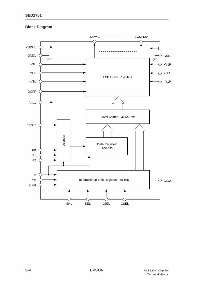
SED1751
5–4 EPSON MLS Driver Chip SetTechnical Manual
VDDHL
GNDL
+V1L
VCL
–V1L
DOFF
GNDR
+V1R
VCR
–V1R
CIO2
LCD Driver: 120-bits
Level Shifter: 3x120-bits
Dec
oder
Bi-directional Shift Register: 30-bits
Data Register:120-bits
VCC
TEST1
LP
YD
CIO1
COM 1 COM 120
SHL SEL LSEL CSEL
FR
F1
F2
Block Diagram

SED1751
MLS Driver Chip Set EPSON 5–5Technical Manual
Explanation of Each BlockShift Register
This is a bi-directional shift register used for transmitting common data. The display data shifts on thefalling edge of LP.
Level Shifter
The level shifter is a voltage level converter circuit which converts the signal voltage level from a logicsystem level to the LC driver system voltage level.
LCD Driver
The LCD driver outputs the LC drive voltage.The relationship between the display blanking signal DOFF, the field recognition signals F1 & F2, the ACsignal FR, and the common output voltage is as follows:
DOFF H LFR L H —
F1,F2 1,1 0,1 1,0 0,0 1,1 0,1 1,0 0,0 —Line 1 +V1 +V1 –V1 +V1 –V1 –V1 +V1 –V1 VC
Line 2 –V1 +V1 +V1 +V1 +V1 –V1 –V1 –V1 VC
Line 3 +V1 –V1 +V1 +V1 –V1 +V1 –V1 –V1 VC
Line 4 +V1 +V1 +V1 –V1 –V1 –V1 –V1 +V1 VC
Voltage level relationships: + V1 > VC > –V1 (VC is the center voltage level)
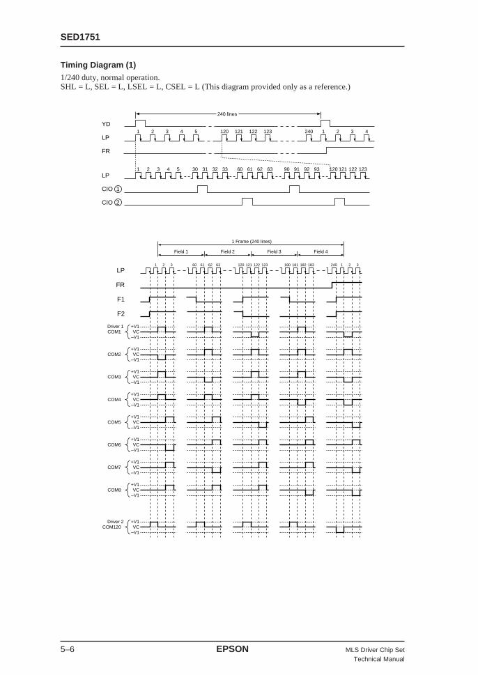
SED1751
5–6 EPSON MLS Driver Chip SetTechnical Manual
Timing Diagram (1)
1/240 duty, normal operation.SHL = L, SEL = L, LSEL = L, CSEL = L (This diagram provided only as a reference.)
+V1VC
–V1
F2
F1
FR
LP
Driver 1COM1
+V1VC
–V1COM2
+V1VC
–V1COM3
+V1VC
–V1COM4
+V1VC
–V1COM5
+V1VC
–V1COM6
+V1VC
–V1COM7
+V1VC
–V1COM8
+V1VC
–V1
Driver 2COM120
Field 1 Field 2 Field 3
1 Frame (240 lines)
Field 4
1 2 3 60 61 62 63 120 121 122 123 180 181 182 183 240 1 2 3
1
1 2 3 4 5 30 31 32 33 60 61 62 63 90 91 92 93 120 121 122 123
2 3 4 5
240 lines
120 121 122 123 240 1 2 3 4YD
LP
FR
LP
CIO 1
CIO 2

SED1751
MLS Driver Chip Set EPSON 5–7Technical Manual
Timing Diagram (2)
1/240 duty, 1/2 H operation.SHL = L, SEL = L, LSEL = H, CSEL = L (This diagram provided only as a reference.)
+V1VC
–V1
F2
F1
FR
LP
Driver 1COM1
+V1VC
–V1COM2
+V1VC
–V1COM3
+V1VC
–V1COM4
+V1VC
–V1COM5
+V1VC
–V1COM6
+V1VC
–V1COM7
+V1VC
–V1COM8
+V1VC
–V1
Driver 2COM120
Field 1 Field 2 Field 3
1 Frame (240 lines)
Field 4
2/240 2/1 2/60 2/61 2/120 2/121 2/180 2/181 2/240 2/1
1/1 1/1 1/61 1/62 1/121 1/122 1/181 1/182 1/1 1/1
1/1
1/1
2/1
1/2
2/2
1/3 1/30
2/30
1/31
2/31
1/60
2/60
1/61
2/61
1/90
2/90
1/91
2/91
1/120
2/120
1/121
2/121
2/1 1/2 2/2 1/3
240 lines
1/120 2/120 1/121 2/121 2/240 1/1 2/1 1/2 2/2YD
LP
FR
LP
CIO
CIO
1
2
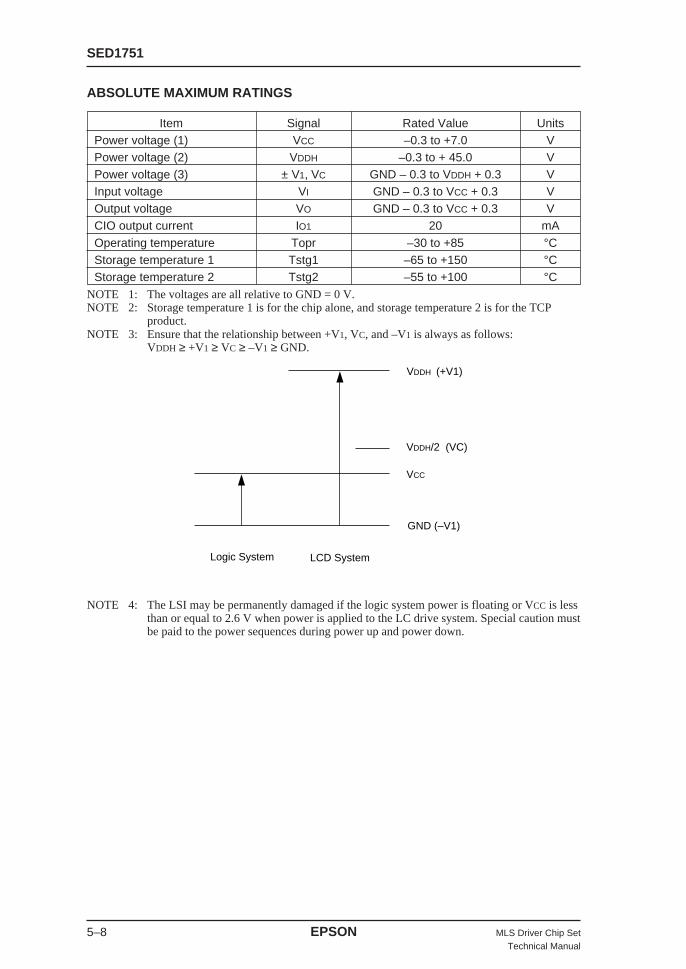
SED1751
5–8 EPSON MLS Driver Chip SetTechnical Manual
ABSOLUTE MAXIMUM RATINGS
Item Signal Rated Value UnitsPower voltage (1) VCC –0.3 to +7.0 VPower voltage (2) VDDH –0.3 to + 45.0 VPower voltage (3) ± V1, VC GND – 0.3 to VDDH + 0.3 VInput voltage VI GND – 0.3 to VCC + 0.3 VOutput voltage VO GND – 0.3 to VCC + 0.3 VCIO output current IO1 20 mAOperating temperature Topr –30 to +85 °CStorage temperature 1 Tstg1 –65 to +150 °CStorage temperature 2 Tstg2 –55 to +100 °C
NOTE 1: The voltages are all relative to GND = 0 V.NOTE 2: Storage temperature 1 is for the chip alone, and storage temperature 2 is for the TCP
product.NOTE 3: Ensure that the relationship between +V1, VC, and –V1 is always as follows:
VDDH ≥ +V1 ≥ VC ≥ –V1 ≥ GND.
NOTE 4: The LSI may be permanently damaged if the logic system power is floating or VCC is lessthan or equal to 2.6 V when power is applied to the LC drive system. Special caution mustbe paid to the power sequences during power up and power down.
VCC
GND (–V1)
VDDH/2 (VC)
VDDH (+V1)
Logic System LCD System

SED1751
MLS Driver Chip Set EPSON 5–9Technical Manual
Electrical CharacteristicsDC Characteristics
Unless otherwise noted, GND = 0 V, VCC = + 5.0 V ± 10%, Ta = –30 to 85°C
Item Signal ParameterApplicable
Min Typ Max UnitTerminals
Power Supply VCC VCC 2.7 5.0 5.5 VVoltage (1)
Range Operating VDDH Function VDDH 8.0 42.0 VVoltages
Power Supply +V1 Recommended Value +V1 VDDH VVoltage (2)
Power SupplyVC Recommended Value VC VDDH/2 VVoltage (3)
Power Supply –V1 Recommended Value –V1 GND VVoltage (4)
High-level Input VIH 0.8VCC VVoltage
VCC = 2.7 to 5.5VLow-level Input VIL 0.2VCC VVoltage
High-level OutputVOH
IOH =VCC–0.4 VVoltage
VCC = 2.7 to 5.5V –0.3mA
CIO1,CIO2Low-level Output VOL
IOL = 0.4 VVoltage 0.3mA
Input Leakage Current ILI GND ≤ VIN ≤ VCC 2.0 µA
Input/Output LeakageILI/O GND ≤ VIN ≤ VCC CIO1,CIO2 5.0 µACurrent
Static Current IGNDVDDH = 14.0~42.0V GND 25 µAVIH = VCC, VIL = GND
∆VON = 0.5 VVDDH = 0.55 0.7
Output Resistance RCOM Recommended +30.0V COM1 to
kΩparameter VDDH = COM120
0.5 0.7 +40.0V
VCC = +5.0 V, VIH = VCC
VIL = GND, fLP = 16.8 kHz 10 25Average Operating fFR = 70 Hz,Consumption Current ICC Input data: 1/240 No load VCC µA(1) VCC = 3.0 V
All other parameters 7 17the same as VCC = 5.0 V.
VDDH = +V1 = +30.0 V,Average Operating VC = VDDH/2, –V1 = 0.0 V,Consumption Current IDDH VCC = 5.0 V VDDH 6 13 µA(2) All other parameters
the same as the ICC item.
Input TerminalCI Freq. = 1 MHz 10 pFCapacity
Chip aloneInput/Output Terminal
CI/O Ta = 25°C CIO1,CIO2 18 pFCapacity
CIO1,CIO2,FR,YD,LP,SHL,SEL,
LSEL,CSEL,DOFF,F1,F2,
TEST1
LP,YD,SHL,SEL,LSEL,CSEL,F1,
F2,DOFF,TEST1,FR
LP,YD,SHL,SEL,LSEL,CSEL,F1,F2,DOFF,TEST1,FR
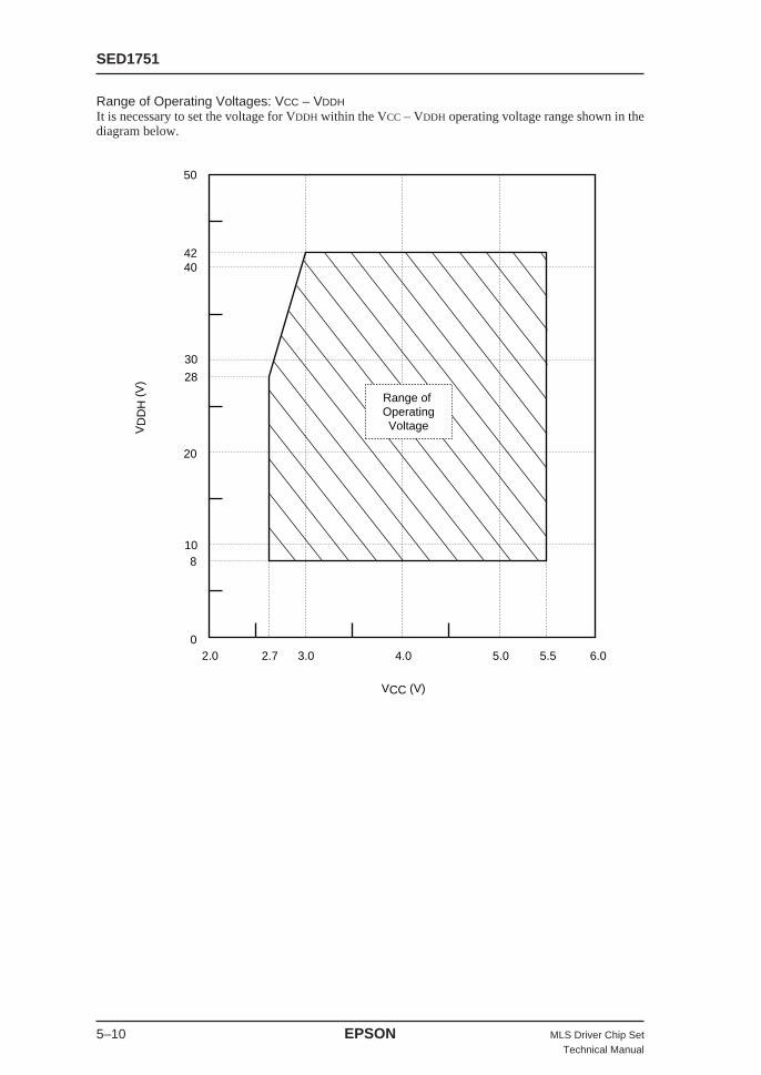
SED1751
5–10 EPSON MLS Driver Chip SetTechnical Manual
Range of Operating Voltages: VCC – VDDHIt is necessary to set the voltage for VDDH within the VCC – VDDH operating voltage range shown in thediagram below.
Range of OperatingVoltage
50
4240
30
20
10
28
8
02.0 3.02.7 4.0
VCC (V)
VD
DH
(V
)
5.0 6.05.5
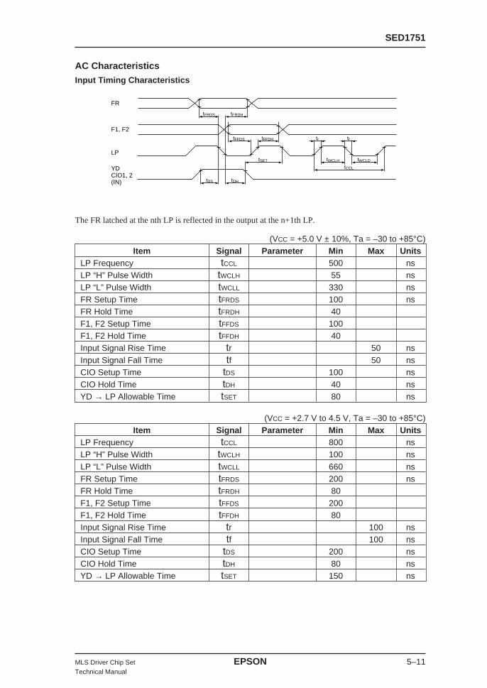
SED1751
MLS Driver Chip Set EPSON 5–11Technical Manual
AC CharacteristicsInput Timing Characteristics
The FR latched at the nth LP is reflected in the output at the n+1th LP.
tDS tDH
tSET tWCLH tWCLD
tCCL
tFFDS tFFDH tr tf
tFRDS tFRDH
FR
F1, F2
LP
YDCIO1, 2(IN)
(VCC = +5.0 V ± 10%, Ta = –30 to +85°C)Item Signal Parameter Min Max Units
LP Frequency tCCL 500 nsLP “H” Pulse Width tWCLH 55 nsLP “L” Pulse Width tWCLL 330 nsFR Setup Time tFRDS 100 nsFR Hold Time tFRDH 40F1, F2 Setup Time tFFDS 100F1, F2 Hold Time tFFDH 40Input Signal Rise Time tr 50 nsInput Signal Fall Time tf 50 nsCIO Setup Time tDS 100 nsCIO Hold Time tDH 40 nsYD → LP Allowable Time tSET 80 ns
(VCC = +2.7 V to 4.5 V, Ta = –30 to +85°C)Item Signal Parameter Min Max Units
LP Frequency tCCL 800 nsLP “H” Pulse Width tWCLH 100 nsLP “L” Pulse Width tWCLL 660 nsFR Setup Time tFRDS 200 nsFR Hold Time tFRDH 80F1, F2 Setup Time tFFDS 200F1, F2 Hold Time tFFDH 80Input Signal Rise Time tr 100 nsInput Signal Fall Time tf 100 nsCIO Setup Time tDS 200 nsCIO Hold Time tDH 80 nsYD → LP Allowable Time tSET 150 ns

SED1751
5–12 EPSON MLS Driver Chip SetTechnical Manual
Output Timing Characteristics
tpdCDOF
tpdCCL
tpdDOC
LP
DOFF
COMOutput
CIO1, 2(OUT)
(VCC = 5.0 V ± 10%, VDDH = +14.0 to +42.0 V, Ta = –30 to +85°C)Item Signal Parameter Min Max Units
Delay time from LP to CIO output tpdDOC CL = 15 pF 300 nsDelay time from LP to COM output tpdCCL VDDH = 350 nsDelay time from DOFF to COM output tpdCDOF 14.0 V to 40.0 V 700 ns
(VCC = +2.7 V to 4.5 V, VDDH = +14.0 to +28.0 V, Ta = –30 to +85°C)Item Signal Parameter Min Max Units
Delay time from LP to CIO output tpdDOC CL = 15 pF 600 nsDelay time from LP to COM output tpdCCL VDDH = 500 nsDelay time from DOFF to COM output tpdCDOF 14.0 V to 40.0 V 1400 ns

SED1751
MLS Driver Chip Set EPSON 5–13Technical Manual
The Power SupplyMethod of Forming Each Voltage Level
VCC
GND
Logic SystemLCD Controller
CapacitorCoupling
Logic System LCD SystemSED1580D0B
Logic System LCD SystemSED1751D0B
VDDx
VSSx
VDDy
VSSy
V3
VC VC
V1
–V1
V2
–V2–V3
When the SED1580 and the SED1751 are used to form an extremely low power module system, the powerrelationships as shown in the figure above between the SED1580 and SED1751 logic systems, and the LCDsystem power supply, and the LCD controller power supply are optimal.In this case, care is required when it comes to signal propagation in the logic system.LCD Controller → SED1580 DirectLCD Controller → SED1751 Capacitor coupling is requiredSED1580 → SED1751 Capacitor coupling is requiredSED1751 → SED1580 Capacitor coupling is required
Cautions at Power Up and Power Down
Because the voltage level in the LCD system is high voltage, if the logic system power supply of this LSIis floating or if VCC is 2.6 V or less when the LCD system high voltage (30 V or above) is applied, or ifthe LCD drive signal is output before the voltage level that is applied to the LCD system has stabilized,then there is the risk that there will be an over current condition in this LSI, resulting in permanent damageto this LSI.It is recommended that the display OFF function (DOFF) is used until the LCD system voltage stabilizesto insure that the LCD drive output power level is at the VC level.Be sure to follow the sequences below when turning the power supplies ON and OFF:
When turning the power supply ON:Logic system ON → LCD drive system ON, or simultaneously ON.
When turning the power supply OFF:LCD drive system OFF → Logic system OFF, or simultaneously OFF.
As a countermeasure to guard against over current conditions, it is effective to insert a high-speed fuse ora guard resistance in series with the LC power supply. The guard resistance value must be optimizeddepending on the capacity of the LC cell.

SED1751
5–14 EPSON MLS Driver Chip SetTechnical Manual
Example of ConnectionLarge Screen LCD Structure Diagram
EIO1BSELLSELF1O~F2OF2SF1SSELCAYDFRLPXSCLDOFFD0~7EIO2
160
SE
D15
80
EIO1BSELLSELF1O~F2OF2SF1SSELCAYDFRLPXSCLDOFFD0~7EIO2
160
SE
D15
80
EIO1BSELLSELF1O~F2OF2SF1SSELCAYDFRLPXSCLDOFFD0~7EIO2
160
SE
D15
80
160
CIO
1Y
DLP F
RD
OF
FS
HL
SE
LLS
EL
CS
EL
F1~
F2
CIO
2
DU
0~7
FS
2F
S1
SH
LU YD
FR LP
XS
CL
DO
FF
LSE
LS
EL
SH
LY
SC
L
SH
LL
DL0
~7
120SED1751
CIO
1Y
DLP F
RD
OF
FS
HL
SE
LLS
EL
CS
EL
F1~
F2
CIO
2
120SED1751
CIO
1Y
DLP F
RD
OF
FS
HL
SE
LLS
EL
CS
EL
F1~
F2
CIO
2
120SED1751
CIO
1Y
DLP F
RD
OF
FS
HL
SE
LLS
EL
CS
EL
F1~
F2
CIO
2
120SED1751
EIO2D0~7
DOFFXSCL
LPFRYDCA
SHLF1SF2S
F1O~F2OLSELBSELEIO1
160
SE
D15
80
EIO2D0~7
DOFFXSCL
LPFRYDCA
SHLF1SF2S
F1O~F2OLSELBSELEIO1
160
SE
D15
80
EIO2D0~7
DOFFXSCL
LPFRYDCA
SHLF1SF2S
F1O~F2OLSELBSELEIO1
160
SE
D15
80
EIO2D0~7
DOFFXSCL
LPFRYDCA
SHLF1SF2S
F1O~F2OLSELBSELEIO1
160
SE
D15
80
640
× 48
0 D
OT
1/24
0 D
UT
Y
Controller
EIO1BSELLSELF1O~F2OF2SF1SSELCAYDFRLPXSCLDOFFD0~7EIO2
SE
D15
80

SED1751
MLS Driver Chip Set EPSON 5–15Technical Manual
Example of External Connections
(Rear surface should be P
1 coated.)(R
ear surface should be P1 coated.)
(Rear surface
should be P
1 coated.)
Detail draw
ing for the test pad sectionO
utput terminal pattern shape
Specifications :
Base : E
upirex-S? , 75?u?m
Copper foil : 31P
(14.25mm
)
Sn plated
Product pitch : 31P
(14.25mm
)
Solder resist position tolerance : ±0.3
(Molding range) (Molding range)
(Rear surface should be P1 coated.)
(Molding range)
(Molding range)
SCI7500F0A

SCI7500F0A
MLS Driver Chip Set EPSON iTechnical Manual
Contents
OVERVIEW ................................................................................................................................... 6-1
TERMINAL FUNCTIONS .............................................................................................................. 6-4
EXPLANATIONS OF FUNCTIONS............................................................................................... 6-8
ELECTRICAL CHARACTERISTICS ........................................................................................... 6-15
EXAMPLE OF CONNECTIONS (REFERENCE) ........................................................................ 6-20
EXTERNAL DIMENSIONS (REFERENCE) ................................................................................ 6-22
EXTERNAL SHAPE OF THE CHIP (SCI7500D0A) ..................................................................... 6-23
COORDINATES OF RESPECTIVE PAD CENTERS ................................................................. 6-24
SCI7500F0A
MLS Driver Chip Set EPSON 6–1Technical Manual
OVERVIEWDescriptionThe SCI7500F0A is a four-line simultaneous selection method MLS (Multi Line Selection) drive powersupply IC for driving liquid crystal displays. Using its CMOS charge pump-type high-efficiency voltageconverter circuit, the chip is able to generate all the bias voltages required for the four-line MLS drive basedon a single 3.0 V power supply input.When a system is structured from column (segment) drivers such as the SED1580, row (common) driverssuch as the SED1751, and this IC, this structure is able to produce a module with extremely low powerconsumption when compared to a conventional drive method.Moreover, even greater power conservation is possible when combined with an LCD controller that canpause data transmission (a controller such as the SED1360).
Features• Power Supply Voltage: 2.4 V to 3.6 V single-input power supply• Low Consumption Current: 340 µA (in 6 × step-up mode, TYP)• Standby Current: 5 µA (MAX)• High Voltage Conversion Efficiency: 88% (6 × step-up mode, TYP)• Generates all bias voltages required for 4-line MLS driving.
An external contrast adjustment function can also be attached.• Equipped with an internal charge pump-type DC/DC voltage converter circuit.
Depending on the terminal settings, the chip can be switched between 5 × step-up (compatible with 1/200 duty) and 6 × step-up (compatible with 1/240 duty).
• Built-in electric charge discharging circuit for the liquid crystal drive current (VL).• Internal “power off” function using an external signal (XSLP).• Equipped internally with a liquid crystal drive polarity reverse signal generator circuit.• The terminal settings can be used to set the range of time for the polarity reversal to 2H to 17H.• Recommended panel size: VGA, 6.3" or less• Product being shipped in QFP form ........................ (QFP12-48 pin) SCI7500F0A
Product being shipped in chip form ........................ SCI7500D0A
• This product not designed for resistance to radiation.

SCI7500F0A
6–2 EPSON MLS Driver Chip SetTechnical Manual
Liquid CrystalDrive Polarity
Reverse SignalGenerator Circuit
VL Discharge Circuit
Column Driver VoltageConversion Circuit
Row Driver Voltage Conversion Circuit
Row Driver Logic CircuitPart Power Supply
Voltage Generator Circuit
VH Voltage GeneratorControl Circuit
TimingSignal
GeneratorCircuit
C3P
C3N
V2
VDD
VSS
L3
L2
L1
L0
FR
XFR
LP
XSLP
–V2
C4P
C4N
C1P
C1N
C2P
C2N
C1PB
C1NB
–V3B
HC
C5P
C5N
C6N
VEM
VEE
C8N
VDDy
VL
XBB
C7N
AB
–V3
Figure 1: Block Diagram
Block Diagram

SCI7500F0A
MLS Driver Chip Set EPSON 6–3Technical Manual
Explanation of Block Diagram Liquid Crystal Drive Polarity Reverse Signal Generator Circuit
This circuit generates the reverse polarity signal FR from the 1H period pulse signal LP. Pins L0 to L3can be used to set the polarity reversal interval to 2H to 17H. Moreover, so that it will be possible todrive the top and bottom screens in a 2-screen drive panel in opposite phases, this IC outputs two signalswith opposite polarities of each other (FR, XFR).
Timing Signal Generator CircuitThis circuit generates the clock for the charge pump from the 1H period pulse signal LP. When thedisplay off control signal XSLP is set to the VSS level, the clock stops and the voltage converteroperation stops.
Column Driver Voltage Conversion CircuitThis circuit generates the V2, –V2, and –V3 voltage levels required for column driving.
Row Driver Voltage Conversion CircuitThis generates the voltage (VEE) required for generating the power supply voltages (VH, VL) requiredfor the row drivers. Using VDD as the reference, this generates either a 5 × or 6 × voltage level in thenegative direction relative to the input power supply voltage. A terminal can be used to switch betweenthe step-up modes. The contrast adjustment function is performed through the use of an external emitterfollower circuit to adjust VEE to generate VL.
Row Driver Logic Circuit Part Power Supply Voltage Generator Circuit This generates the power supply voltage (VDDy) required by the row driver logic circuit part. Thisgenerates a voltage that is higher than the voltage level VL by an amount equal to VDD–VSS.
VH Voltage Generator Control CircuitThis is a circuit for generating the power supply voltage (VH) required for the row driver. The VHvoltage can be generated by an external MOS transistor and this circuit.
VL Discharge CircuitAt power off or display off, this circuit discharges the charge remaining on the row driver negativevoltage level-side power supply voltage terminal (VL).

SCI7500F0A
6–4 EPSON MLS Driver Chip SetTechnical Manual
1 2 3 4 5 6 7 8 9 10 11 12
VL
C8N
VD
Dy
C7N
VS
SV
EE
C6N
VE
MC
5N HC
NC
C5P
VD
DC
3PN
CV
2C
3NV
SS
C1P
VD
DC
2P–V
3N
CN
C
36 35 34 33 32 31 30 29 28 27 26 25
242322212019181716151413
C2NC1NVSS–V3C4P–V2C4NVDDC1PBVSSC1NB–V3B
L0L1L2L3
VSSLPFR
XFRXSLPXTST
ABXBB
373839404142434445464748
Terminal Terminal Terminal Terminal Terminal Terminal Terminal TerminalNo. Name No. Name No. Name No. Name1 VL 13 –V3B 25 — 37 L02 C8N 14 C1NB 26 — 38 L13 VDDy 15 VSS 27 –V3 39 L24 C7N 16 C1PB 28 C2P 40 L35 VSS 17 VDD 29 VDD 41 VSS
6 VEE 18 C4N 30 C1P 42 LP7 C6N 19 –V2 31 VSS 43 FR8 VEM 20 C4P 32 C3N 44 XFR9 C5N 21 –V3 33 V2 45 XSLP
10 HC 22 VSS 34 — 46 XTST11 — 23 C1N 35 C3P 47 AB12 C5P 24 C2N 36 VDD 48 XBB
TERMINAL FUNCTIONSTerminal Layout Diagram
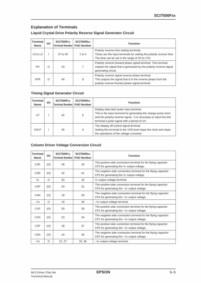
SCI7500F0A
MLS Driver Chip Set EPSON 6–5Technical Manual
Explanation of TerminalsLiquid Crystal Drive Polarity Reverse Signal Generator Circuit
Timing Signal Generator Circuit
Column Driver Voltage Conversion Circuit
TerminalI/O
SCI7500F0A SCI7500D0AFunction
Name Terminal Number PAD Number
Polarity reverse time setting terminals.L0 to L3 I 37 to 40 1 to 4 These are the input terminals for setting the polarity reverse time.
The time can be set in the range of 2H to 17H.
Polarity reverse forward phase signal terminal. This terminalFR O 43 7 outputs the signal that is generated by the polarity reverse signal
generating circuit.
Polarity reverse signal reverse phase terminal.XFR O 44 8 This outputs the signal that is in the reverse phase from the
polarity reverse forward phase signal terminal.
TerminalI/O
SCI7500F0A SCI7500D0AFunction
Name Terminal Number PAD Number
Display data latch pulse input terminal.
LP I 42 6This is the input terminal for generating the charge pump clockand the polarity reverse signal. It is necessary to input into thisterminal a pulse signal with a period of 1H.
The display off control signal terminal.XSLP I 45 9 Setting this terminal to the VSS level stops the clock and stops
the operations of the voltage converter.
TerminalI/O
SCI7500F0A SCI7500D0AFunction
Name Terminal Number PAD Number
C3P (O) 35 43The positive-side connection terminal for the flying capacitorCP3 for generating the V2 output voltage.
C3N (O) 32 41The negative-side connection terminal for the flying capacitorCP3 for generating the V2 output voltage.
V2 O 33 42 V2 output voltage terminal.
C4P (O) 20 31The positive-side connection terminal for the flying capacitorCP4 for generating the –V2 output voltage.
C4N (O) 18 29The negative-side connection terminal for the flying capacitorCP4 for generating the –V2 output voltage.
–V2 O 19 30 –V2 output voltage terminal.
C1P (O) 30 39The positive-side connection terminal for the flying capacitorCP1 for generating the –V3 output voltage.
C1N (O) 23 34The negative-side connection terminal for the flying capacitorCP1 for generating the –V3 output voltage.
C2P (O) 28 37The positive-side connection terminal for the flying capacitorCP2 for generating the –V3 output voltage.
C2N (O) 24 35The negative-side connection terminal for the flying capacitorCP2 for generating the –V3 output voltage.
–V3 O 21, 27 32, 36 –V3 output voltage terminal.

SCI7500F0A
6–6 EPSON MLS Driver Chip SetTechnical Manual
Row Driver Voltage Conversion Circuit
Common Driver Logic Circuit Part Power Supply Voltage Generator Circuit
TerminalI/O
SCI7500F0A SCI7500D0AFunction
Name Terminal Number PAD Number
The negative-side connection terminal for the flying capacitorC8N (O) 2 14 CP8 for generating the VDDy output voltage. The positive
connection terminal for CP8 is the same as C1PB.
The row driver logic circuit part power supply output terminal.This generates the power supply voltage required for the row
VDDy O 3 15 driver logic circuit part. The output is higher than the VL level inthe positive direction by an amount equal to the differencebetween VDD and VSS.
TerminalI/O
SCI7500F0A SCI7500D0AFunction
Name Terminal Number PAD Number
C1PB (O) 16 27The positive-side connection terminal for the flying capacitorCP1B and CP8 for generating the –V3B output voltage.
C1NB (O) 14 25The negative-side connection terminal for the flying capacitorCP1B for generating the –V3B output voltage.
The negative V3B output voltage terminal. This is an output–V3B O 13 24 terminal equipped as the middle voltage level for generating the
VEE output voltage.
The step-up mode select terminal. When this terminal is tied VSS,HC I 10 22 then the chip is put into 5 X step-up mode. However, when it is
connected to –3B, the chip is set to 6 X step-up mode.
C5P (O) 12 23The positive-side connection terminal for the flying capacitorCP5 and CP6 for generating the VEM output voltage.
C5N (O) 9 21The negative-side connection terminal for the flying capacitorCP5 for generating the VEM output voltage.
The VEM output voltage terminal.VEM O 8 20 This is an output terminal equipped as the middle voltage level for
generating the VEE output voltage.
The negative-side connection terminal for the flying capacitorC6N (O) 7 19 CP6 for generating the VEE output voltage. (The positive-side of
CP6 is C5P.)
The VEE output voltage terminal.
VEE O 6 18By changing the HC terminal interconnection method, it ispossible to switch between the 5-level step-up mode and the6-level step-up mode.
SCI7500F0A
MLS Driver Chip Set EPSON 6–7Technical Manual
VH Voltage Generator Control Circuit
TerminalI/O
SCI7500F0A SCI7500D0AFunction
Name Terminal Number PAD Number
The VH output voltage generator clock terminal A.AB O 47 11 This is the clock output terminal for the external N-channel MOS
transistor control.
The VH output voltage generator clock terminal B.XBB O 48 12 This is the clock output terminal for the external P-channel MOS
transistor control.
The negative-side connection terminal for the flying capacitorC7N (O) 4 16 CP7 for generating the VH output voltage. The positive-side
connection terminal corresponds to the external transistor.
TerminalI/O
SCI7500F0A SCI7500D0AFunction
Name Terminal Number PAD Number
VDD I17, 29, 28, 38
Input power supply terminals (positive).36 *1 44 *1
VSS I5, 15, 22, 5, 17, 26
Input power supply terminals (negative).31, 41 *1 33, 40 *1
Note: *1 Please connect these power supply terminals externally.
Power Supply Terminals <Note 1>
The Test Circuit
VL Discharge Circuit
TerminalI/O
SCI7500F0A SCI7500D0AFunction
Name Terminal Number PAD Number
This is the row driver negative voltage level power supply voltageterminal.
VL I 1 13The VL signal that is used to adjust the contrast is input to thisterminal. This serves as the power supply for the VH voltagegenerator control circuit.XSLP operates the discharge circuit at the VSS level.
TerminalI/O
SCI7500F0A SCI7500D0AFunction
Name Terminal Number PAD Number
XTST I 46 10This is a test terminal.Insure that this terminal is always tied to the VDD level.

SCI7500F0A
6–8 EPSON MLS Driver Chip SetTechnical Manual
Column Driver(SED1580)
Common Driver(SED1751)
Common Driver(SED1751)
Power Supply IC(SCI7500)
ExternalComponents
LCD Controller(SED1360)
V3
VCV2, –V2, –V3
VSS
VDD
VEM, VEE, VL
VDD
VSS
VH, VL VC
VDDyColumn Driver
(SED1580)
V3
VC
Liquid CrystalPanel
Figure 2: The System Configuration
Overview of OperationThe SCI7500F0A is a power supply IC for operating the 4-line simultaneous selection method MLS (MultiLine Selection) driver LCDs. Using its CMOS charge pump-type high-efficiency voltage converter circuit,this chip can produce all of the bias voltages necessary for a 4-line MLS driving based on a single 3.0 Vpower supply.The voltage levels produced are as follows:• The liquid crystal drive power supply voltages required for the column drivers (V3 = VDD, V2, VC =
VSS, –V2, –V3).• The liquid crystal drive power supply voltages required for the row drivers (VH, VC = VSS, VL).• The power supply voltages for the logic circuits of the row driver (VDDy).
However, the row driver low voltage-side power supply voltage (VL) requires an external bipolar transistorfor adjusting the contrast. Moreover, external MOS transistors (2SK***, 2SJ***) are required forgenerating the row driver high-level power supply voltage (VH).Depending on a terminal setting, the chip can switch between 6 X step-up mode and 5 X step-up mode,with 1/240 duty and 1/200 duty, respectively. Consequently, it is possible to obtain the required voltageswith maximum efficiency.An example of a system structure diagram for the power supply interconnections is given below:
EXPLANATIONS OF FUNCTIONS

SCI7500F0A
MLS Driver Chip Set EPSON 6–9Technical Manual
6
5
4
3
2
1
0
-1
-2
-3
-4
-5
-6
VH VH
VDD
VSS
VDD
VSS
VDD
VSS
[SED1360]Controller
[SCI7500]Power Supply IC +
External Components
[SED1580]ColumnDriver
[SED1751]Row Driver
V2
–V2–V3
VEMVDDy
VLVEE
V3V2VC–V2–V3
VDDy
VL
When in 6 × step-up mode When in 5 × step-up mode(when HC is connected to –V 3B). (when HC is connected to V SS).
Voltage level when Voltage level whenLogical Formula V DD = 3.0V Logical Formula V DD = 3.0V
and VSS = 0V and VSS = 0V
VH = –VL = 5 (VDD–VSS)–α 15.0–α VH = –VL = 4 (VDD–VSS)–α 12.0–αV3 = VDD–VSS 3.0 V3 = VDD–VSS 3.0
V2 = 1/2 (VDD–VSS) 1.5 V2 = 1/2 (VDD–VSS) 1.5
VC = VSS 0 VC = VSS 0
–V2 = –1/2 (VDD–VSS) –1.5 –V2 = –1/2 (VDD–VSS) –1.5
–V3 = –V3B = –(VDD–VSS) –3.0 –V3 = –V3B = –(VDD–VSS) –3.0
VEM = –3 (VDD–VSS) –9.0 VEM = –2 (VDD–VSS) –6.0
VDDy = –4 (VDD–VSS) + α –12.0 + α VDDy = –3 (VDD–VSS) + α –9.0 + αVL = –5 (VDD–VSS) + α –15.0 + α VL = –4 (VDD–VSS) + α –12.0 + αVEE = –5 (VDD–VSS) –15.0 VEE = –4 (VDD–VSS) –12.0
Where α = variable ≥ 0 (contrast adjustment)
The relationships between voltage levels in the system shown in Figure 2 are given in the table below.
The logical formulas for each of the voltage levels is as given below:
Figure 3: The Relationships Between Voltages Within the System (in 6 × step-up mode)
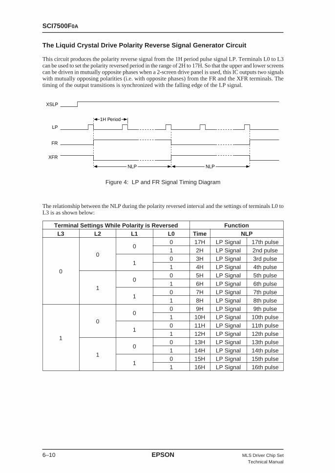
SCI7500F0A
6–10 EPSON MLS Driver Chip SetTechnical Manual
1H Period
NLP
XSLP
NLP
LP
FR
XFR
Terminal Settings While Polarity is Reversed FunctionL3 L2 L1 L0 Time NLP
00 17H LP Signal 17th pulse
01 2H LP Signal 2nd pulse
10 3H LP Signal 3rd pulse
01 4H LP Signal 4th pulse
00 5H LP Signal 5th pulse
11 6H LP Signal 6th pulse
10 7H LP Signal 7th pulse1 8H LP Signal 8th pulse
00 9H LP Signal 9th pulse
01 10H LP Signal 10th pulse
10 11H LP Signal 11th pulse
11 12H LP Signal 12th pulse
00 13H LP Signal 13th pulse
11 14H LP Signal 14th pulse
10 15H LP Signal 15th pulse1 16H LP Signal 16th pulse
Figure 4: LP and FR Signal Timing Diagram
This circuit produces the polarity reverse signal from the 1H period pulse signal LP. Terminals L0 to L3can be used to set the polarity reversed period in the range of 2H to 17H. So that the upper and lower screenscan be driven in mutually opposite phases when a 2-screen drive panel is used, this IC outputs two signalswith mutually opposing polarities (i.e. with opposite phases) from the FR and the XFR terminals. Thetiming of the output transitions is synchronized with the falling edge of the LP signal.
The relationship between the NLP during the polarity reversed interval and the settings of terminals L0 toL3 is as shown below:
The Liquid Crystal Drive Polarity Reverse Signal Generator Circuit
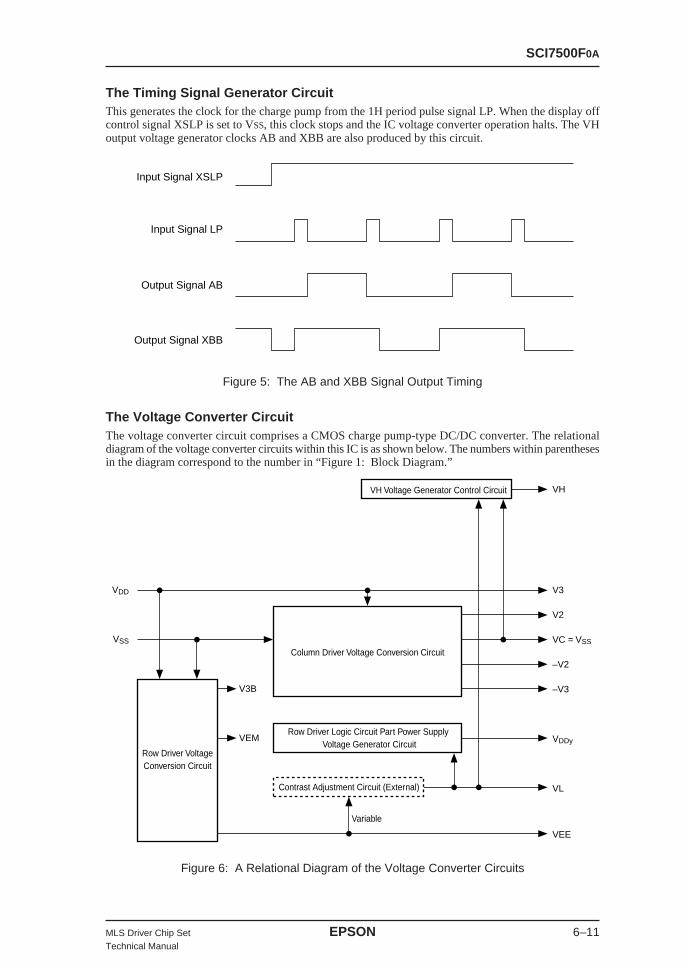
SCI7500F0A
MLS Driver Chip Set EPSON 6–11Technical Manual
Input Signal XSLP
Input Signal LP
Output Signal AB
Output Signal XBB
Figure 5: The AB and XBB Signal Output Timing
Contrast Adjustment Circuit (External)
Variable
Column Driver Voltage Conversion Circuit
VDD
VSS
V3B
VH
V3
V2
VC = VSS
–V2
–V3
VDDy
VL
VEE
VEM
Row Driver VoltageConversion Circuit
Row Driver Logic Circuit Part Power Supply Voltage Generator Circuit
VH Voltage Generator Control Circuit
Figure 6: A Relational Diagram of the Voltage Converter Circuits
The Timing Signal Generator CircuitThis generates the clock for the charge pump from the 1H period pulse signal LP. When the display offcontrol signal XSLP is set to VSS, this clock stops and the IC voltage converter operation halts. The VHoutput voltage generator clocks AB and XBB are also produced by this circuit.
The Voltage Converter CircuitThe voltage converter circuit comprises a CMOS charge pump-type DC/DC converter. The relationaldiagram of the voltage converter circuits within this IC is as shown below. The numbers within parenthesesin the diagram correspond to the number in “Figure 1: Block Diagram.”
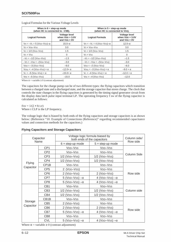
SCI7500F0A
6–12 EPSON MLS Driver Chip SetTechnical Manual
When in 6 × step-up mode When in 5 × step-up mode(when HC is connected to –V3B). (when HC is connected to V SS).
Voltage level Voltage levelLogical Formula when V DD = 3.0V Logical Formula when V DD = 3.0V
and VSS = 0V and VSS = 0V
VH = –VL = 5 (VDD–VSS)–a 15.0–α VH = –VL = 4 (VDD–VSS)–α 12.0–αV3 = VDD–VSS 3.0 V3 = VDD–VSS 3.0
V2 = 1/2 (VDD–VSS) 1.5 V2 = 1/2 (VDD–VSS) 1.5
VC = VSS 0 VC = VSS 0
–V2 = –1/2 (VDD–VSS) –1.5 –V2 = –1/2 (VDD–VSS) –1.5
–V3 = –V3B = –(VDD–VSS) –3.0 –V3 = –V3B = –(VDD–VSS) –3.0
VEM = –3 (VDD–VSS) –9.0 VEM = –2 (VDD–VSS) –6.0
VDDy = –4 (VDD–VSS) + α –12.0+ α VDDy = –3 (VDD–VSS) + α –9.0 + αVL = –5 (VDD–VSS) + α –15.0+ α VL = –4 (VDD–VSS) + α –12.0 + αVEE = –5 (VDD–VSS) –15.0 VEE = –4 (VDD–VSS) –12.0
Where α = variable ≥ 0 (contrast adjustment)
CapacitorVoltage logic formula biased by
Column side/Name
both ends of the capacitorsRow side
6 × step-up mode 5 × step-up modeCP1 VDD–VSS VDD–VSS
CP2 VDD–VSS VDD–VSSColumn Side
CP3 1/2 (VDD–VSS) 1/2 (VDD–VSS)
FlyingCP4 1/2 (VDD–VSS) 1/2 (VDD–VSS)
CapacitorCP1B VDD–VSS VDD–VSS
CP5 2 (VDD–VSS) VDD–VSS
CP6 2 (VDD–VSS) 2 (VDD–VSS) Row sideCP7 5 (VDD–VSS) –α 4 (VDD–VSS) –αCP8 5 (VDD–VSS) –α 4 (VDD–VSS) –αCB1 VDD–VSS VDD–VSS
CB3 1/2 (VDD–VSS) 1/2 (VDD–VSS) Column sideCB4 1/2 (VDD–VSS) 1/2 (VDD–VSS)
StorageCB1B VDD–VSS VDD–VSS
CapacitorCB5 2 (VDD–VSS) VDD–VSS
CB6 2 (VDD–VSS) 2 (VDD–VSS)Row side
CB7 5 (VDD–VSS) –α 4 (VDD–VSS) –αCB8 VDD–VSS VDD–VSS
CVL 5 (VDD–VSS) –α 4 (VDD–VSS) –αWhere α = variable ≥ 0 (contrast adjustment)
Logical Formulas for the Various Voltage Levels
The capacitors for the charge pump can be of two different types: the flying capacitors which transitionbetween a charged state and a discharged state, and the storage capacitor that stores charge. The clock thatcontrols the state changes in the flying capacitors is generated by the timing signal generator circuit fromthe display data latch pulse input terminal LP. The operating frequency f sw of the flying capacitor iscalculated as follows:
fSW = 1/(2 × tCLP)Where t CLP is the LP frequency.
The voltage logic that is biased by both ends of the flying capacitors and storage capacitors is as shownbelow: (Reference “10. Example of Connections (Reference)” regarding recommended capacitancevalues and connection methods for the capacitors.)
Flying Capacitors and Storage Capacitors
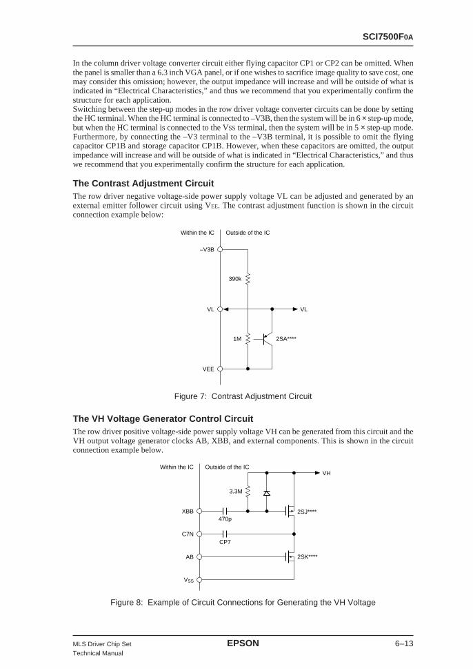
SCI7500F0A
MLS Driver Chip Set EPSON 6–13Technical Manual
Figure 7: Contrast Adjustment Circuit
–V3B
Within the IC Outside of the IC
VL
VEE
VL
390k
1M 2SA****
XBB
C7N
AB
VSS
Within the IC Outside of the ICVH
2SJ****
2SK****
3.3M
470p
CP7
In the column driver voltage converter circuit either flying capacitor CP1 or CP2 can be omitted. Whenthe panel is smaller than a 6.3 inch VGA panel, or if one wishes to sacrifice image quality to save cost, onemay consider this omission; however, the output impedance will increase and will be outside of what isindicated in “Electrical Characteristics,” and thus we recommend that you experimentally confirm thestructure for each application.Switching between the step-up modes in the row driver voltage converter circuits can be done by settingthe HC terminal. When the HC terminal is connected to –V3B, then the system will be in 6 × step-up mode,but when the HC terminal is connected to the VSS terminal, then the system will be in 5 × step-up mode.Furthermore, by connecting the –V3 terminal to the –V3B terminal, it is possible to omit the flyingcapacitor CP1B and storage capacitor CP1B. However, when these capacitors are omitted, the outputimpedance will increase and will be outside of what is indicated in “Electrical Characteristics,” and thuswe recommend that you experimentally confirm the structure for each application.
The Contrast Adjustment CircuitThe row driver negative voltage-side power supply voltage VL can be adjusted and generated by anexternal emitter follower circuit using VEE. The contrast adjustment function is shown in the circuitconnection example below:
The VH Voltage Generator Control CircuitThe row driver positive voltage-side power supply voltage VH can be generated from this circuit and theVH output voltage generator clocks AB, XBB, and external components. This is shown in the circuitconnection example below.
Figure 8: Example of Circuit Connections for Generating the VH Voltage
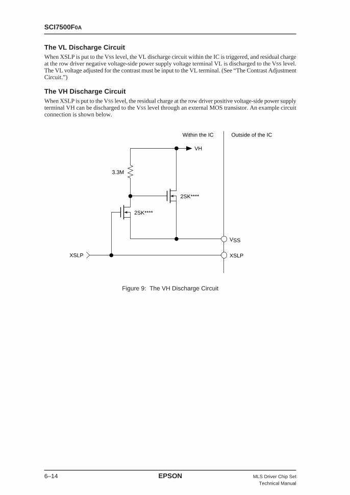
SCI7500F0A
6–14 EPSON MLS Driver Chip SetTechnical Manual
Figure 9: The VH Discharge Circuit
VSS
XSLP
Within the IC Outside of the IC
VH
3.3M
XSLP
2SK****
2SK****
The VL Discharge CircuitWhen XSLP is put to the VSS level, the VL discharge circuit within the IC is triggered, and residual chargeat the row driver negative voltage-side power supply voltage terminal VL is discharged to the VSS level.The VL voltage adjusted for the contrast must be input to the VL terminal. (See “The Contrast AdjustmentCircuit.”)
The VH Discharge CircuitWhen XSLP is put to the VSS level, the residual charge at the row driver positive voltage-side power supplyterminal VH can be discharged to the VSS level through an external MOS transistor. An example circuitconnection is shown below.

SCI7500F0A
MLS Driver Chip Set EPSON 6–15Technical Manual
VSS = 0V
Item SignalRated Value
Units NotesMinimum Maximum
Input power supply voltage 1 VDD — 3.7 V VDD terminalInput power supply voltage 2 VL VEE-0.3 0.3 V VL terminal
The L3 to L0, LP,Input terminal voltage VI –0.3 VDD + 3.0 V XSLP, and XTST
terminalsInput current IDD — 10 mA VDD, VL
Output current 1 IV2 — 6 mA V2 terminalOutput current 2 I-V2 — 6 mA -V2 terminalOutput current 3 I-V3 — 5 mA -V3 terminalOutput current 4 I VEE — 1 mA VEE terminalOutput current 5 I VDDy — 0.1 mA VDDy terminalAllowable loss Pd — 100 mW Ta ≤ 55 °COperating temperature Topr –30 85 °C —Storage temperature Tstg –55 150 °C —Soldering temperature and time Tsol — 260 × 10 °C × S At the lead
Notes: *1 Do not apply a voltage from the outside to the output terminals nor to the capacitorconnection terminals.
Notes: *2 Operating failures and/or permanent damage may occur if this chip is used underconditions exceeding the absolute maximum ratings listed above. Moreover, the reliabilityof this chip may be dramatically compromised even if the chip continues to functionnormally for a time.
ELECTRICAL CHARACTERISTICSThe Absolute Maximum Ratings
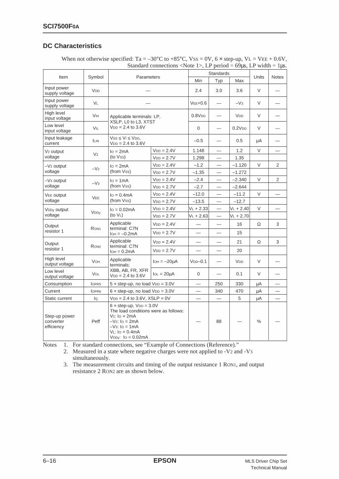
SCI7500F0A
6–16 EPSON MLS Driver Chip SetTechnical Manual
When not otherwise specified: Ta = –30°C to +85°C, VSS = 0V, 6 × step-up, VL = VEE + 0.6V,Standard connections <Note 1>, LP period = 69µs, LP width = 1µs.
Item Symbol ParametersStandards
Units NotesMin Typ Max
Input power VDD — 2.4 3.0 3.6 V —supply voltage
Input power VL — VEE+0.6 — –V3 V —supply voltage
High level VIH Applicable terminals: LP, 0.8VDD — VDD V —input voltageXSLP, L0 to L3, XTST
Low levelVIL VDD = 2.4 to 3.6V 0 — 0.2VDD V —input voltage
Input leakage ILINVSS ≤ VI ≤ VDD, –0.5 — 0.5 µA —
current VDD = 2.4 to 3.6V
V2 outputV2
IO = 2mA VDD = 2.4V 1.148 — 1.2 V —voltage (to VSS) VDD = 2.7V 1.298 — 1.35
–V2 output–V2
IO = 2mA VDD = 2.4V –1.2 — –1.120 V 2voltage (from VSS) VDD = 2.7V –1.35 — –1.272
–V3 output–V3
IO = 1mA VDD = 2.4V –2.4 — –2.340 V 2voltage (from VSS) VDD = 2.7V –2.7 — –2.644
VEE outputVEE
IO = 0.4mA VDD = 2.4V –12.0 — –11.2 V —voltage (from VSS) VDD = 2.7V –13.5 — –12.7
VDDy outputVDDy
IO = 0.02mA VDD = 2.4V VL + 2.33 — VL + 2.40 V —voltage (to VL) VDD = 2.7V VL + 2.63 — VL + 2.70
Output Applicable VDD = 2.4V — — 16 Ω 3
resistor 1RON1 terminal: C7N
IOH = –0.2mA VDD = 2.7V — — 15
Output Applicable VDD = 2.4V — — 21 Ω 3
resistor 1 RON2 terminal: C7NIOH = 0.2mA VDD = 2.7V — — 20
High levelVOH Applicable IOH = –20µA VDD–0.1 — VDD V —output voltage terminals:
Low level VOLXBB, AB, FR, XFR
IOL = 20µA 0 — 0.1 V —output voltage VDD = 2.4 to 3.6V
Consumption IOPR5 5 × step-up, no load VDD = 3.0V — 250 330 µA —
Current IOPR6 6 × step-up, no load VDD = 3.0V — 340 470 µA —
Static current IQ VDD = 2.4 to 3.6V, XSLP = 0V — — 5 µA —
6 × step-up, VDD = 3.0VThe load conditions were as follows:
Step-up power V2: IO = 2mAconverter Peff –V2: IO = 2mA — 88 — % —efficiency –V3: IO = 1mA
VL: IO = 0.4mAVDDy: IO = 0.02mA
Notes 1. For standard connections, see “Example of Connections (Reference).”2. Measured in a state where negative charges were not applied to -V2 and -V3
simultaneously.3. The measurement circuits and timing of the output resistance 1 RON1, and output
resistance 2 RON2 are as shown below.
DC Characteristics

SCI7500F0A
MLS Driver Chip Set EPSON 6–17Technical Manual
VDD V
VDD × 6VV
A
VC7N
1C7N = 0.2mA
1 C7NR ON1 =
V C7N
VDD
VSS
C7N
VEE
SCI7500
VDD VVDD × 6V
VDD × 6-0.6V V
A
VC7N
1C7N = 0.2mA
1 C7NR ON2 =
V C7N
VDD
VSS
C7N
VEE
VL
SCI7500
XSLP
R ON1
LP
R ON2
Figure 12: The Measurement Timingusing RON1 and RON2
Figure 10: The RON1 MeasurementCircuit Figure
Figure 11: The RON2 MeasurementCircuit
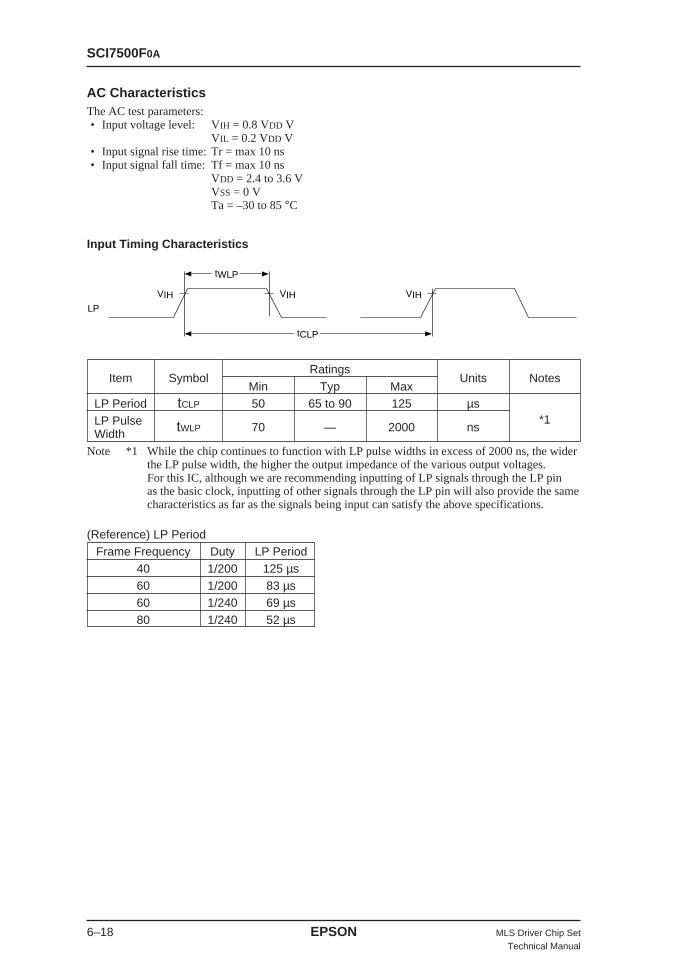
SCI7500F0A
6–18 EPSON MLS Driver Chip SetTechnical Manual
Input Timing Characteristics
tCLP
LP
VIH VIH VIH
tWLP
Item SymbolRatings
Units NotesMin Typ Max
LP Period tCLP 50 65 to 90 125 µsLP Pulse tWLP 70 — 2000 ns
*1Width
Note *1 While the chip continues to function with LP pulse widths in excess of 2000 ns, the widerthe LP pulse width, the higher the output impedance of the various output voltages.For this IC, although we are recommending inputting of LP signals through the LP pinas the basic clock, inputting of other signals through the LP pin will also provide the samecharacteristics as far as the signals being input can satisfy the above specifications.
(Reference) LP PeriodFrame Frequency Duty LP Period
40 1/200 125 µs60 1/200 83 µs60 1/240 69 µs80 1/240 52 µs
AC CharacteristicsThe AC test parameters:• Input voltage level: VIH = 0.8 VDD V
VIL = 0.2 VDD V• Input signal rise time: Tr = max 10 ns• Input signal fall time: Tf = max 10 ns
VDD = 2.4 to 3.6 VVSS = 0 VTa = –30 to 85 °C
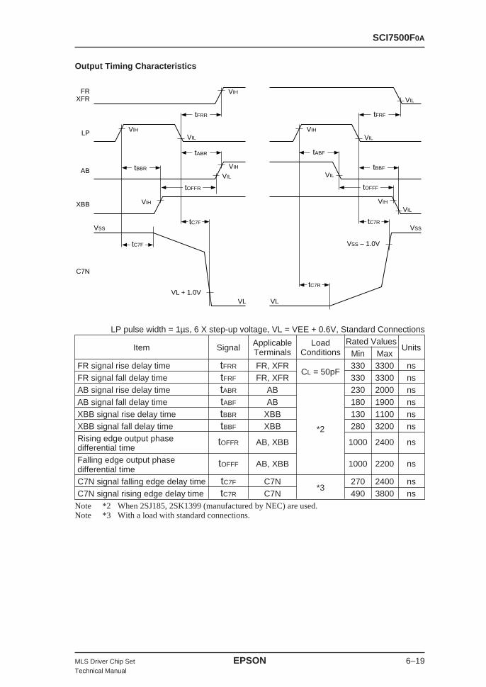
SCI7500F0A
MLS Driver Chip Set EPSON 6–19Technical Manual
tFRR
tABR
tFRF
tABF
tC7F tC7R
tC7F
tC7R
tBBR tBBF
tOFFR tOFFF
VIHFRXFR
LP
AB
XBB
C7N
VIH
VIH
VSS VSS
VIH
VIL
VIL
VIH
VIL
VIL
VIL
VIL
VIH
VL + 1.0V
VSS – 1.0V
VL VL
LP pulse width = 1µs, 6 X step-up voltage, VL = VEE + 0.6V, Standard Connections
Item Signal Applicable Load Rated ValuesUnitsTerminals Conditions Min Max
FR signal rise delay time tFRR FR, XFRCL = 50pF
330 3300 nsFR signal fall delay time tFRF FR, XFR 330 3300 nsAB signal rise delay time tABR AB 230 2000 nsAB signal fall delay time tABF AB 180 1900 nsXBB signal rise delay time tBBR XBB 130 1100 nsXBB signal fall delay time tBBF XBB *2 280 3200 nsRising edge output phase tOFFR AB, XBB 1000 2400 nsdifferential timeFalling edge output phase tOFFF AB, XBB 1000 2200 nsdifferential timeC7N signal falling edge delay time tC7F C7N
*3270 2400 ns
C7N signal rising edge delay time tC7R C7N 490 3800 nsNote *2 When 2SJ185, 2SK1399 (manufactured by NEC) are used.Note *3 With a load with standard connections.
Output Timing Characteristics

SCI7500F0A
6–20 EPSON MLS Driver Chip SetTechnical Manual
4417,29,36
5,15,2231,41
40
39
38
37
46
XFR
FR
C3P
C3N
V2
VSS
–V2
C4P
C4N
–V3
C1P
C1N
C2P
C2N
C1PB
C1NB
–V3B
HC
C5N
C5P
C6N
VEM
C8N
VDDy
VL
VEE
XBB
C7N
AB
VSS
VDD
VSS
L3
L2
L1
L0
XTST
LP
XSLP
LP
XSLP
VDD
VSS
43
35
32
33
19
20
18
21,27
30
23
28
24
16
14
13
10
9
12
7
8
2
3
1
6
48
4
47
3.3M3.3M
CB8
CP6
CP5
CP1B
CP2
CP1
CP4
CP3
CB3
CB4
2SJ****
2SK****
2SK****
2SA****
2SK****
VH
VL
VDDy
–V3
–V2
VC
V2
V3
470p
CP7
CB1B
CB1
CP8 CVL
CB7
CB5
CB6 500k
510k
To Row Drivers
To Column Driver
42
45
EXAMPLE OF CONNECTIONS (REFERENCE)Standard Connections for the 6 × step-up mode.
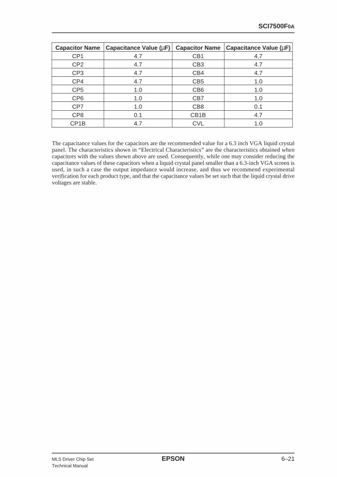
SCI7500F0A
MLS Driver Chip Set EPSON 6–21Technical Manual
Capacitor Name Capacitance Value ( µF) Capacitor Name Capacitance Value ( µF)CP1 4.7 CB1 4.7CP2 4.7 CB3 4.7CP3 4.7 CB4 4.7CP4 4.7 CB5 1.0CP5 1.0 CB6 1.0CP6 1.0 CB7 1.0CP7 1.0 CB8 0.1CP8 0.1 CB1B 4.7
CP1B 4.7 CVL 1.0
The capacitance values for the capacitors are the recommended value for a 6.3 inch VGA liquid crystalpanel. The characteristics shown in “Electrical Characteristics” are the characteristics obtained whencapacitors with the values shown above are used. Consequently, while one may consider reducing thecapacitance values of these capacitors when a liquid crystal panel smaller than a 6.3-inch VGA screen isused, in such a case the output impedance would increase, and thus we recommend experimentalverification for each product type, and that the capacitance values be set such that the liquid crystal drivevoltages are stable.

SCI7500F0A
6–22 EPSON MLS Driver Chip SetTechnical Manual
EXTERNAL DIMENSIONS (REFERENCE)Note: These dimensions are subject to change without notice.
7±0.1
9±0.4
2536
7±0.
1
9±0.
4
13
24
INDEX
0.18121
48
37
1.4±
0.1
0.1
1.7m
ax
1
0.5±0.2
0°10°
0.125±0.05
0.5+0.1–0.05
Plastic QFP12-48 pin

SCI7500F0A
MLS Driver Chip Set EPSON 6–23Technical Manual
EXTERNAL SHAPE OF THE CHIP (SCI7500D 0A)
PAD layout
Chip size: 3.48mm × 3.44mm
Chip thickness: 400µm ± 30µm
PAD hole size: 100µm × 100µm
Substrate potential: VDD
DIE number: F7500D0A
35
36
37
38
39
40
41 (0, 0)
Y
X
42
34 33 32 31 30 29 28 27 26 25 24
C2N C1N VSS –V3 C4P –V2 C4N VDD C1PB VSS C1NB –V3B
23
22
21
20
19
18
17
16
15
14
13
C5P
HC
C5N
VEM
C6N
VEE
VSS
C7N
VDDy
C8N
VL
121110987654321
XBBABXTSTXSLPXFRFRLPVSSL3L2L1L0
44
43
–V3
C2P
VDD
C1P
VSS
C3N
V2
VDD
C3P
DIENUMBER
3.48mm
3.44mm

SCI7500F0A
6–24 EPSON MLS Driver Chip SetTechnical Manual
COORDINATES OF RESPECTIVE PAD CENTERSUnit: µm
1 L0 –1431.2 –1554.4
2 L1 –1191.2
3 L2 –951.2
4 L3 –711.2
5 VSS –471.2
6 LP –280.8
7 FR –40.8
8 XFR 199.2
9 XSLP 439.2
10 XTST 679.2
11 AB 919.2
12 XBB 1159.2
13 VL 1574.4 –1264.8
14 C8N –1024.8
15 VDDy –784.8
16 C7N –544.8
17 VSS –304.8
18 VEE –64.8
19 C6N 175.2
20 VEM 415.2
21 C5N 655.2
22 HC 895.2
23 C5P 1574.4 1135.2
24 –V3B 1235.2 1554.4
25 C1NB 995.2
26 VSS 755.2
27 C1PB 475.2
28 VDD 235.2
29 C4N –4.8
30 –V2 –244.8
31 C4P –484.8
32 –V3 –724.8
33 VSS –964.8
34 C1N –1204.8
35 C2N –1444.8
36 –V3 –1574.4 935.2
37 C2P 655.2
38 VDD 415.2
39 C1P 175.2
40 VSS –64.8
41 C3N –304.8
42 V2 –544.8
43 C3P –1024.8
44 VDD –1264.8
PAD No. PAD name X Y PAD No. PAD name X Y
AMERICAEPSON ELECTRONICS AMERICA, INC.HEADQUARTERS1960 E. Grand AveEl Segundo, CA 90245, U.S.A.Phone : +1-310-955-5300 Fax : +1-310-955-5400
SALES OFFICESWest150 River Oaks ParkwaySan Jose, CA 95134, U.S.A.Phone : +1-408-922-0200 Fax : +1-408-922-0238
Central1450 East American Lane Suite 1550Schaumburg, IL 60173, U.S.A.Phone : +1-847-517-7667 Fax : +1-847-517-7601
101 Virginia Street, Suite 290Crystal Lake, IL 60014, U.S.A.Phone : +1-815-455-7630 Fax : +1-815-455-7633
Northeast301 Edgewater Place, Suite 120Wakefield, MA 01880, U.S.A.Phone : +1-781-246-3600 Fax : +1-781-246-5443
Southeast4300 Six Forks Road, Suite 430Raleigh, NC 27609, U.S.A.Phone : +1-919-781-7667 Fax : +1-919-781-6778
1700 Spinnaker DriveAlptaretta, GA 30005, U.S.A.Phone : +1-770-754-4872 Fax : +1-770-753-0601
EUROPEEPSON EUROPE ELECTRONICS GmbHHEADQUARTERSRiesstrasse 1580992 Muenchen, GERMANYPhone : +49- (0) 89-14005-0 Fax : +49- (0) 89-14005-110
- GERMANY -SALES OFFICEBreidenbachstrasse 46D-51373 Leverkusen, GERMANYPhone : +49- (0) 214-83070-0 Fax : +49- (0) 214-83070-10
- UNITED KINGDOM -UK BRANCH OFFICEG6 Doncastle House, Doncastle RoadBracknell, Berkshire RG12 8PE, ENGLANDPhone : +44- (0) 1344-381700 Fax : +44- (0) 1344-381701
- FRANCE -FRENCH BRANCH OFFICE1 Avenue de l’ Atlantique, LP 915 Les ConquerantsZ.A. de Courtaboeuf 2, F-91976 Les Ulis Cedex, FRANCEPhone : +33- (0) 1-64862350 Fax : +33- (0) 1-64862355
ASIA- HONG KONG, CHINA -EPSON HONG KONG LTD.20/F., Harbour Centre, 25 Harbour RoadWanchai, HONG KONGPhone : +852-2585-4600 Fax : +852-2827-4346Telex : 65542 EPSCO HX
- CHINA -SHANGHAI EPSON ELECTRONICS CO., LTD.4F, Bldg., 27, No. 69, Gui Jing RoadCaohejing, Shanghai, CHINAPhone : 21-6485-5552 Fax : 21-6485-0775
- TAIWAN, R.O.C. -EPSON TAIWAN TECHNOLOGY & TRADING LTD.10F, No. 287,Nanking East Road, Sec. 3Taipei, TAIWAN, R.O.C.Phone : 02-2717-7360 Fax : 02-2712-9164Telex : 24444 EPSONTB
HSINCHU OFFICE13F-3, No.295, Kuang-Fu Road, Sec. 2HsinChu 300, TAIWAN, R.O.C.Phone : 03-573-9900 Fax : 03-573-9169
- SINGAPORE -EPSON SINGAPORE PTE., LTD.No. 1 Temasek Avenue, #36-00Millenia Tower, SINGAPORE 039192Phone : +65-337-7911 Fax : +65-334-2716
- KOREA -SEIKO EPSON CORPORATIONKOREA OFFICE10F, KLI 63 Bldg., 60 Yoido-DongYoungdeungpo-Ku, Seoul, 150-010, KOREAPhone : 02-784-6027 Fax : 02-767-3677
- JAPAN -SEIKO EPSON CORPORATIONELECTRONIC DEVICES MARKETING DIVISION
Electronic Device Marketing DepartmentIC Marketing & Engineering Group421-8, Hino, Hino-shi, Tokyo 191-8501, JAPANPhone: +81-(0)42-587-5816 Fax: +81-(0)42-587-5624
ED International Marketing Department I (Europe & U.S.A.)421-8, Hino, Hino-shi, Tokyo 191-8501, JAPANPhone: +81-(0)42-587-5812 Fax: +81-(0)42-587-5564
ED International Marketing Department II (Asia)421-8, Hino, Hino-shi, Tokyo 191-8501, JAPANPhone: +81-(0)42-587-5814 Fax: +81-(0)42-587-5110
International Sales Operations

MLS Driver Chip SetLCD driver with RAM
First issue Nov., 1997 Printed Oct., 1998 in Japan H A
Electronic Devices Information on Epson WWW Server
SEIKO EPSON CORPORATION ELECTRONIC DEVICES MARKETING DIVISION
http://www.epson.co.jp