
Circuit and Full Custom Layout Design of 8-bit Comparator ...
73
Circuit and Full Custom Layout Design of 8-bit Comparator using 0.25μm CMOS Technology PARTHA SARATI DAS Student No: 082238(F) DEPARTMENT OF ELECTRICAL AND ELECTRONIC ENGINEERING DHAKA UNIVERSITY OF ENGINEERING & TECHNOLOGY, GAZIPUR SEPTEMBER, 2012
Transcript of Circuit and Full Custom Layout Design of 8-bit Comparator ...
Circuit and Full Custom Layout Design of 8-bit
Comparator using 0.25µm CMOS Technology
PARTHA SARATI DAS
Student No: 082238(F)
DEPARTMENT OF ELECTRICAL AND ELECTRONIC ENGINEERING
DHAKA UNIVERSITY OF ENGINEERING & TECHNOLOGY, GAZIPUR
SEPTEMBER, 2012

Circuit and Full Custom Layout Design of 8-bit
Comparator using 0.25µm CMOS Technology
A Project Report Submitted in partial fulfillment of the requirements for the award of the
degree of
MASTER OF ENGINNEERING IN
ELECTRICAL AND ELECTRONIC ENGINEERING By
Partha Sarati Das
Student No. 082238 F Session: 2011-2012
Under Supervision of
Dr. Md. Anwarul Abedin
Professor
DEPARTMENT OF ELECTRICAL AND ELECTRONIC ENGINEERING
DHAKA UNIVERSITY OF ENGINEERING & TECHNOLOGY, GAZIPUR
SEPTEMBER, 2012

The project report titled “Circuit and Full Custom Layout Design of 8-bit Comparator using 0.25µm CMOS Technology” submitted by Partha Sarati Das, Student No. 082238F, Session: 2011-2012 has been accepted as satisfactory in partial fulfillment of the requirement for the Degree of Master of Engineering in Electrical and Electronic Engineering on September 18, 2012.
Board of Examiners
1. ………………………… (Dr. Md. Bashir Uddin) Chairman Professor and Head Department of EEE DUET, Gazipur 2. ………………………..................... (Engr. Mohammad Abdul Mannan) Member Professor Department of EEE DUET, Gazipur 3. ……………………………... (Dr. Md. Anwarul Abedin) Member Professor (Supervisor) Department of EEE DUET, Gazipur 4. …………………………… (Dr. Md. Saifuddin Faruk) Member Assistant Professor Department of EEE DUET, Gazipur 5. …………………....................... (Dr. Md. Ziaur Rahman Khan) Member Associate Professor (External) Department of EEE BUET, Dhaka

Declaration
It is hereby declared that this Project or any part of it has not been submitted elsewhere for the award of any degree of diploma. Signature of the candidate ------------------------ Partha Sarati Das


i
Acknowledgement First of all, I like to thank and express my gratefulness to Almighty God for giving me the
strength and energy to complete this project successfully.
I wish to acknowledge my gratefulness to my project supervisor Dr. Md. Anwarul Abedin,
Professor, Department of Electrical and Electronic Engineering (EEE), Dhaka University of
Engineering and Technology, Gazipur, for his valuable advices, endless patience, important
suggestions, constant and energetic supervision, constructive criticism, and above all scholarly
guidance from beginning to the end of the project work. However, I believe, it is not possible to
properly acknowledge his effort in written words.
I would like to express my heartiest gratefulness to all of my teachers here at the Department of
EEE, Dhaka University of Engineering and Technology. Discussions with many of them have
enriched my conception and knowledge about this project. I want to give heartiest thanks to my
class mates.
Finally, last but not the least I would like to thank my parents and family members who have
given me a tremendous support and inspiration.

ii
ABSTRACT
In this project, a compact and low power 8-bit comparator is designed using 0.25µm CMOS
technology. The circuit produces 3 bit output: first output is active when first input is less than
second input, second output is active when first input is equal to second input and third output is
active when first input is greater than second input. Our approach is first to build up a 1-bit
comparator as one component and then connect eight such kind of 1-bit comparator together.
In this project the design is implemented through two ways. One form uses the same component
N times. This component that is instantiated repeatedly has a two 1-bit primary input, three 1-bit
control input and three 1-bit output interface.
The three control inputs are the three comparison (relation) outputs from the previous pair of
bits. However, the first comparator in this design requires the control signals being driven by
ground and high voltage in order to initialize the system and guarantee functionality.
The second design implementation is that uses a basic single bit comparator with no control
inputs for the first comparator block. Then N-1 cascading comparators are used to finish of the
design (i.e. all of the design is iterative except for the first component). The advantage to this
design is that it has a clean, straight forward input interface. There is no need to ground or power
any input pins because the initial component has been designed without the control inputs. The
outputs of the first comparator are the control inputs for the second comparator (or the first
cascading single bit comparator). The completely iterative design is composed completely of the
cascading single bit comparator.

iii
CONTENTS Page No. ACKNOWLEDGEMENT i ABSTRACT ii CONTENTS iii LIST OF FIGURES vi CHAPTER 1: INTRODUCTION 1 1.1 Introduction 1 1.1.1 Structured Design 3 1.1.2 Challenges 3 1.2 Objectives 5 1.3 Project Organization 5 CHAPTER 2: COMPARATORS & IT’S APPLICATION 6 2.1 Introduction 6 2.1.1 Digital Comparator 6 2.1.2 Comparator truth tables 7 2.1.3 Implementation 8 2.1.4 Equality 8 2.1.5 Inequality 9 2.2 Voltage Comparator 9
2.2.1 Input Voltage Range 9 2.2.2 Op-Amp voltage comparator 10 2.2.3 Dedicated Voltage Comparator Chips 10
2.3 Key Specifications 11
2.3.1 Speed & Power 11 2.3.2 Hysteresis 11 2.3.3 Output Type 12 2.3.4 Internal Reference 13 2.3.5 Continuous Versus Clocked 13
2.4 Applications 13
2.4.1 Null Detector 13 2.4.2 Zero Crossing Detector 14 2.4.3 Relaxation Oscillator 14 2.4.4 Level shifter 15 2.4.5 Analog to Digital Converter 15
iv
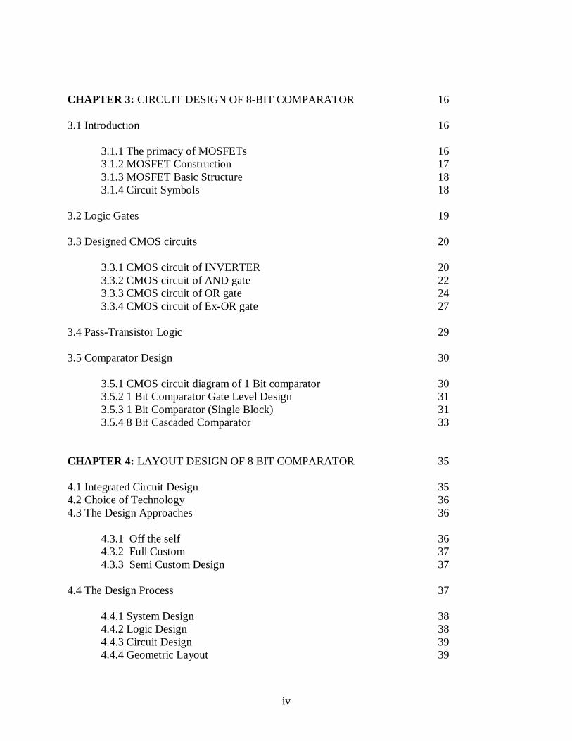
CHAPTER 3: CIRCUIT DESIGN OF 8-BIT COMPARATOR 16 3.1 Introduction 16 3.1.1 The primacy of MOSFETs 16
3.1.2 MOSFET Construction 17 3.1.3 MOSFET Basic Structure 18 3.1.4 Circuit Symbols 18
3.2 Logic Gates 19
3.3 Designed CMOS circuits 20
3.3.1 CMOS circuit of INVERTER 20 3.3.2 CMOS circuit of AND gate 22 3.3.3 CMOS circuit of OR gate 24 3.3.4 CMOS circuit of Ex-OR gate 27
3.4 Pass-Transistor Logic 29 3.5 Comparator Design 30 3.5.1 CMOS circuit diagram of 1 Bit comparator 30 3.5.2 1 Bit Comparator Gate Level Design 31 3.5.3 1 Bit Comparator (Single Block) 31 3.5.4 8 Bit Cascaded Comparator 33
CHAPTER 4: LAYOUT DESIGN OF 8 BIT COMPARATOR 35 4.1 Integrated Circuit Design 35 4.2 Choice of Technology 36 4.3 The Design Approaches 36 4.3.1 Off the self 36 4.3.2 Full Custom 37 4.3.3 Semi Custom Design 37 4.4 The Design Process 37 4.4.1 System Design 38 4.4.2 Logic Design 38 4.4.3 Circuit Design 39 4.4.4 Geometric Layout 39

v
4.4.5 Design Rule Check 39 4.4.6 Fabrication 39 4.5 Layout Design Software (Microwind) 40
4.5.1 Drawing a single MOS 41 4.5.2 Manual Design 41 4.5.3 Process Simulation 42 4.5.4 MOS Characteristics 43 4.5.5 ADD properties for simulation 43
4.6 Layout of CMOS circuit 44
4.6.1 Layout of the designed inverter 44 4.6.3 Layout of the designed 3 input AND gate 46 4.6.5 Layout of the designed 2 input AND gate 48 4.6.7 Layout of the designed 2 input OR gate 50 4.6.9 Layout of the designed 2 input EX-OR gate 52
4.7 Logic Diagram of 1 bit comparator cell 53 4.8 Designed Layout of 1 bit comparator cell 54 4.9 Designed layout of 8 bit comparator 56 4.10 Specification of Designed Test Chip 58
CHAPTER 5: CONCLUSION 59 5.1 Conclusion 59 5.2 Future Scope of Work 59 REFERENCES 61

vi
LIST OF FIGURES Fig. No. Figure Caption Page No 2.1 Truth Table of 1 bit comparator 7
2.2 Truth Table of 2 bit comparator 7
2.3 A simple op-amp comparator 10
2.4 Low Power CMOS Clocked Comparator 12
3.1 Basic structure of MOSFET 18
3.2 Different Types of MOSFET symbol 19
3.3 CMOS circuit diagram of an Inverter (NOT) gate 21
3.4 Block diagram of an Inverter (NOT) gate 22
3.5 Input Output wave shape of an Inverter (NOT) gate 22
3.6 CMOS circuit diagram of 2 input AND gate 23
3.7 Block diagram of a 2 input AND gate 23
3.8 Input Output wave shape of a 2 input AND gate 24
3.9 CMOS circuit diagram of 2 input OR gate 25
3.10 Block diagram of a 2 input OR gate 26
3.11 Input Output wave shape of a 2 input OR gate 26
3.12 CMOS circuit diagram of 2 input Ex-OR gate 27
3.13 Block diagram of a 2 input Ex-OR gate 28
3.14 Input Output wave shape of a 2 input Ex-OR gate 28
3.15 Pass-Transistor Logic Gate 29
3.16 EX-NOR Gate Implemented in Pass-Transistor Logic 29
3.17 CMOS circuit diagram of 1bit comparator 30
3.18 Gate level Design of 1 bit comparator 31
3.19 Block diagram of an 1 bit comparator 31
3.20 Input Output wave shape of an 1 bit comparator output 32
3.21 Block diagram of an 8 Bit Cascaded Comparator 33
3.22 Input Output wave shape of an 8 bit comparator output 34
4.1 Top-down design hierarchy for full custom design 37
4.2 Microwind main window 39

vii
4.3 Symbol of nMOS & pMOS 40
4.4 Minimum width of polysilicon box 41
4.5 Steps of Oxidations 41
4.6 Designed Layout of an Inverter (NOT gate) 43
4.7 Input output wave shape of an Inverter (NOT gate) 44
4.8 Layout of the Designed 3-input and gate 45
4.9 Input Output wave shape of the designed 3-input and gate 46
4.10 Layout of the Designed 2-input and gate 47
4.11 Input Output wave shape of the designed 2-input and gate 48
4.12 Layout of the Designed 2-input or gate 49
4.13 Input Output wave shape of the designed 2-input or gate 50
4.14 Layout of the Designed 2-input ex-or gate 51
4.15 Input Output wave shape of the designed 2-input ex-or gate 52
4.16 Logic Diagram of 1 bit comparator cell 52
4.17 Designed Layout of 1 bit comparator cell 53
4.18 Input output wave shape of 1 bit comparator 54
4.19 Designed Layout of 8 bit comparator cell 55
4.20 Input output wave shape of 8 bit comparator 56

1
CHAPTER 1 Introduction
1.1 Introduction Current society would be unimaginable without electronic gadgets. Nowadays, nobody
can imagine having no internet, computers, TV, mobile phones, etc. and the trend of
dependence on technology is still growing. In this scheme of development, electronic
devices are becoming more and more complex and initial integrated circuits (IC)
developed in the 1950s with a few transistors has grown to current IC with billions of
transistors. This last evolution of ICs, the VLSI (Very Large Scale Integration)
generation, demands a much more sophisticated way of designing than the handmade
approach of the earliest ICs. There is also a big challenge involving the more and more
“narrow” technology as far as CMOS manufacturing process [1] is concerned.
Very-large-scale integration (VLSI) is the process of creating integrated circuits by
combining thousands of transistors into a single chip. VLSI began in the 1970s when
complex semiconductor and communication technologies were being developed. The
microprocessor is a VLSI device.

2
The first semiconductor chips held two transistors each. Subsequent advances added
more and more transistors, and, as a consequence, more individual functions or systems
were integrated over time. The first integrated circuits [2] held only a few devices,
perhaps as many as ten diodes, transistors, resistors and capacitors, making it possible to
fabricate one or more logic gates on a single device. Now known retrospectively as
small-scale integration (SSI), improvements in technique led to devices with hundreds of
logic gates, known as medium-scale integration (MSI). Further improvements led to
large-scale integration (LSI), i.e. systems with at least a thousand logic gates. Current
technology has moved far past this mark and today's microprocessors have many millions
of gates and billions of individual transistors.
At one time, there was an effort to name and calibrate various levels of large-scale
integration above VLSI. Terms like ultra-large-scale integration (ULSI) were used. But
the huge number of gates and transistors available on common devices has rendered such
fine distinctions moot. Terms suggesting greater than VLSI levels of integration are no
longer in widespread use.
As of early 2008, billion-transistor processors are commercially available. This is
expected to become more commonplace as semiconductor fabrication moves from the
current generation of 65 nm processes to the next 45 nm generations (while experiencing
new challenges such as increased variation across process corners). A notable example is
Nvidia's 280 series GPU. This GPU is unique in the fact that almost all of its 1.4 billion
transistors are used for logic, in contrast to the Itanium, whose large transistor count is
largely due to its 24 MB L3 cache. Current designs, as opposed to the earliest devices,
use extensive design automation and automated logic synthesis to lay out the transistors,
enabling higher levels of complexity in the resulting logic functionality. Certain high-
performance logic blocks like the SRAM (Static Random Access Memory) cell, however,
are still designed by hand to ensure the highest efficiency (sometimes by bending or

3
breaking established design rules to obtain the last bit of performance by trading
stability).
1.1.1 Structured Design
Structured VLSI design is a modular methodology originated by Carver Mead and Lynn
Conway for saving microchip area by minimizing the interconnect fabrics area [2-4].
This is obtained by repetitive arrangement of rectangular macro blocks which can be
interconnected using wiring by abutment. An example is partitioning the layout of an
adder into a row of equal bit slices cells. In complex designs this structuring may be
achieved by hierarchical nesting.
Structured VLSI design had been popular in the early 1980s, but lost its popularity later
because of the advent of placement and routing tools wasting a lot of area by routing,
which is tolerated because of the progress of Moore's Law. When introducing the
hardware description language KARL in the mid' 1970s, Reiner Hartenstein coined the
term “structured VLSI design” (originally as “structured LSI design”), echoing Edsger
Dijkstra's structured programming approach by procedure nesting to avoid chaotic
spaghetti-structured programs.
1.1.2 Challenges
As microprocessors become more complex due to technology scaling, microprocessor
designers have encountered several challenges which force them to think beyond the
design plane, and look ahead to post-silicon:
Power usage/Heat dissipation – As threshold voltages have ceased to scale
with advancing process technology, dynamic power dissipation has not scaled
proportionally. Maintaining logic complexity when scaling the design down only
means that the power dissipation per area will go up. This has given rise to

4
techniques such as dynamic voltage and frequency scaling (DVFS) to minimize
overall power.
Process variation – As photolithography techniques tend closer to the
fundamental laws of optics, achieving high accuracy in doping concentrations and
etched wires is becoming more difficult and prone to errors due to variation.
Designers now must simulate across multiple fabrication process corners before a
chip is certified ready for production.
Stricter design rules – Due to lithography and etch issues with scaling, design
rules for layout have become increasingly stringent. Designers must keep ever
more of these rules in mind while laying out custom circuits. The overhead for
custom design is now reaching a tipping point, with many design houses opting to
switch to electronic design automation (EDA) tools to automate their design
process.
Timing/design closure – As clock frequencies tend to scale up, designers are
finding it more difficult to distribute and maintain low clock skew between these
high frequency clocks across the entire chip. This has led to a rising interest in
multicore and multiprocessor architectures, since an overall speedup can be
obtained by lowering the clock frequency and distributing processing.
First-pass success – As die sizes shrink (due to scaling), and wafer sizes go up
(to lower manufacturing costs), the number of dies per wafer increases, and the
complexity of making suitable photomasks goes up rapidly. A mask set for a
modern technology can cost several million dollars. This non-recurring expense
deters the old iterative philosophy involving several “spin-cycles” to find errors in
silicon, and encourages first-pass silicon success. Several design philosophies
have been developed to aid this new design flow, including design for
manufacturing (DFM), design for test (DFT).

5
1.2 Objectives
The goals to be achieved in this project is to design a Modular Circuit and Full Custom
Layout of a 8-bit comparator using 0.25µm CMOS Technology which will be compact
and the main emphasis is on low power. This designed Modular circuit of 8-bit
comparator analyses power dissipation, clock frequency & also delay times of each
parameter of that designed circuit.
1.3 Project Report Organization This project report is organized in this way. Chapter 1 gives history & features of VLSI
design. A basic background of various types of comparators including a brief explanation
about the comparators are explained in Chapter 2. Chapter 3 presents the starting point of
the design i.e. CMOS circuit design with ORCAD. Chapter 4 presents the full custom
layout design of 8 bit Comparator using Microwind. Finally, a concluding remarks and
scope for future work is presented in Chapter 5.

6
CHAPTER 2 Comparators & It’s Application
2.1 Introduction This chapter describes the basic of comparators & its application. The roles of Different
types of comparators & its application are described briefly. The important characteristics
of comparators are explained. Finally consideration is given to the commercially
produced comparators [4] that was basis for practical investigation in this project.
2.1.1 Digital Comparator
A digital comparator [5-6] or magnitude comparator is a hardware electronic device that
takes two numbers as input in binary form and determines whether one number is greater
than, less than or equal to the other number. Comparators are used in a central processing
units (CPU) and microcontrollers. Examples of digital comparator include the CMOS
4063 and 4585 and the TTL 7485 and 74682-89.The analog equivalent of digital

7
comparator is the voltage comparator. Many microcontrollers have analog comparators
on some of their inputs that can be read or trigger an interrupt.
2.1.2 Comparator truth tables
The operation of a single bit digital comparator can be expressed as truth table:
A B A<B A=B A>B
0 0 0 1 0
0 1 1 0 0
1 0 0 0 1
1 1 0 1 0
Fig. 2.1: Truth Table of 1 bit comparator
The operation of a single bit digital comparator can be expressed as truth table:
Inputs Outputs Inputs Outputs
A1 A0 B1 B0 A<B A=B A>B A1 A0 B1 B0 A<B A=B A>B
0 0 0 0 0 1 0 1 0 0 0 0 0 1
0 0 0 1 1 0 0 1 0 0 1 0 0 1
0 0 1 0 1 0 0 1 0 1 0 0 1 0
0 0 1 1 1 0 0 1 0 1 1 1 0 0
0 1 0 0 0 0 1 1 1 0 0 0 0 1
0 1 0 1 0 1 0 1 1 0 1 0 0 1
0 1 1 0 1 0 0 1 1 1 0 0 0 1
0 1 1 1 1 0 0
1 1 1 1 0 1 0
Fig. 2.2: Truth Table of 2 bit comparator

8
2.1.3 Implementation
Consider two 4-bit binary numbers A and B such that
A = A3A2A1A0
B = B3B2B1B0
Here each subscript represents one of the digits in the numbers.
2.1.4 Equality
The binary numbers A and B will be equal if all the pairs of significant digits of both
numbers are equal, i.e.,
A3 = B3, A2 = B2, A1 = B1 and A0 = B0
Since the numbers are binary, the digits are either 0 or 1 and the boolean function for
equality of any two digits Ai and Bi can be expressed as
.
xi is 1 only if Ai and Bi are equal.
For the equality of A and B, all xi variables (for i = 0, 1, 2, 3) must be 1.
So the quality condition of A and B can be implemented using the AND operation as
(A = B) = x3x2x1x0
The binary variable (A=B) is 1 only if all pairs of digits of the two numbers are equal.

9
2.1.5 Inequality
In order to manually determine the greater of two binary numbers inspect the relative
magnitudes of pairs of significant digits, starting from the most significant bit, gradually
proceeding towards lower significant bits until an inequality is found. When an inequality
is found, if the corresponding bit of A is 1 and that of B is 0 then we conclude that A>B.
This sequential comparison can be expressed logically as:
(A>B) and (A < B) are output binary variables, which are equal to 1 when A>B or A<B
respectively.
2.2 Voltage Comparator
A comparator compares the voltages at the + and – inputs. If the + input is at a higher
voltage than the – input the comparator output will be high. If the –input is at a higher
voltage than the + input the comparator output will be low.
2.2.1 Input voltage range
The input voltages must stay within the limits specified by the manufacturer. Early
integrated comparators, like the LM111 family, and certain high-speed comparators like
the LM119 family, require input voltage ranges lower than the power supply voltages
(±15 V vs. 36V). Rail-to-rail comparators allow any input voltages within the power
supply range. When powered from a bipolar (dual rail) supply,
10
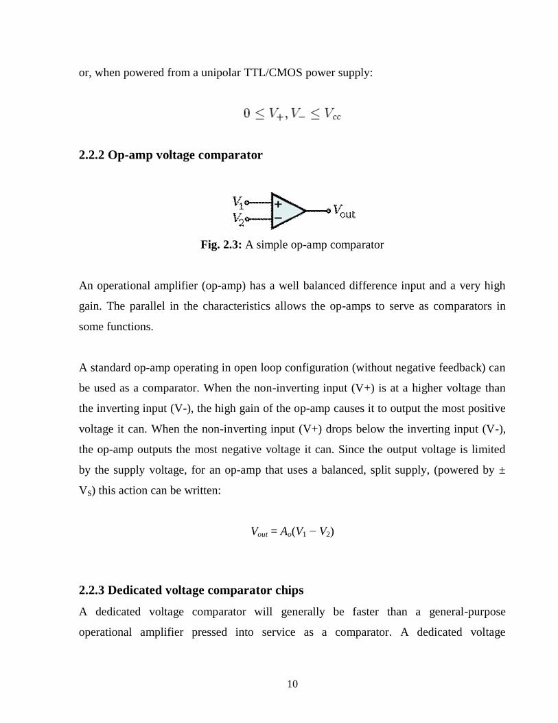
or, when powered from a unipolar TTL/CMOS power supply:
2.2.2 Op-amp voltage comparator
Fig. 2.3: A simple op-amp comparator
An operational amplifier (op-amp) has a well balanced difference input and a very high
gain. The parallel in the characteristics allows the op-amps to serve as comparators in
some functions.
A standard op-amp operating in open loop configuration (without negative feedback) can
be used as a comparator. When the non-inverting input (V+) is at a higher voltage than
the inverting input (V-), the high gain of the op-amp causes it to output the most positive
voltage it can. When the non-inverting input (V+) drops below the inverting input (V-),
the op-amp outputs the most negative voltage it can. Since the output voltage is limited
by the supply voltage, for an op-amp that uses a balanced, split supply, (powered by ±
VS) this action can be written:
Vout = Ao(V1 − V2)
2.2.3 Dedicated voltage comparator chips
A dedicated voltage comparator will generally be faster than a general-purpose
operational amplifier pressed into service as a comparator. A dedicated voltage

11
comparator may also contain additional features such as an accurate, internal voltage
reference, an adjustable hysteresis and a clock gated input.
Inputs Output
− > + Negative
+ > − Floating
With a pull-up resistor and a 0 to +5V power supply, the output takes on the voltages 0 or
+5 and can interface with TTL logic.
2.3 Key specifications of Comparator
It is easy to understand the basic task of a comparator, that is, comparing two voltages or
currents, several parameters must be considered while selecting a suitable comparator:
2.3.1 Speed and power
In general comparators are “fast”, their circuits are not immune to the classic speed-
power tradeoff. High speed comparators use transistors with larger aspect ratios and
hence also consume more power. Depending on the application, select either a
comparator with high speed or one that saves power.
2.3.2 Hysteresis
A comparator normally changes its output state when the voltage between its inputs
crosses through approximately zero volts. Small voltage fluctuations due to noise, always
present on the inputs can cause undesirable rapid changes between the two output states
when the input voltage difference is near zero volts. To prevent this output oscillation, a
small hysteresis of a few millivolts is integrated into many modern comparators. If the

12
comparator does not have internal hysteresis or if the input noise is greater than the
internal hysteresis then an external hysteresis network can be built using positive
feedback from the output to the non-inverting input of the comparator. The resulting
Schmitt trigger circuit gives additional noise immunity and a cleaner output signal.
2.3.3 Output type
Fig. 2.4: Low Power CMOS Clocked Comparator
Because comparators have only two output states, their outputs are near zero or near the
supply voltage. Bipolar rail-to-rail comparators have a common-emitter output that
produces a small voltage drop between the output and each rail. That drop is equal to the
collector-to-emitter voltage of a saturated transistor. When output currents are light,
output voltages of CMOS rail-to-rail comparators, which rely on a saturated MOSFET,
range closer to the rails than their bipolar counterparts.
On the basis of outputs, comparators can also be classified as open drain or push–pull.
Comparators with an open-drain output stage use an external pull up resistor to a positive
supply that defines the logic high level.Open drain comparators can also be used to

13
connect multiple comparators on to a single bus. Push pull output does not need a pull up
resistor and can also source current unlike an open drain output.
2.3.4 Internal reference
The most frequent application for comparators is the comparison between a voltage and a
stable reference. Most comparator manufacturers also offer comparators in which a
reference voltage is integrated on to the chip. Combining the reference and comparator in
one chip not only saves space, but also draws less supply current than a comparator with
an external reference.
2.3.5 Continuous versus clocked
A continuous comparator will output either a “1” or a “0” any time a high or low signal is
applied to its input and will change quickly when the inputs are updated. However, many
applications only require comparator outputs at certain instances, such as in A/D
converters and memory. Higher accuracy and lower power can be achieved with a
clocked (or dynamic) comparator structure, also called a latched comparator. Often
latched comparators employ strong positive feedback for a “regeneration phase” when a
clock is high, and have a “reset phase” when the clock is low. This is in contrast to a
continuous comparator, which can only employ weak positive feedback since there is no
reset period.
2.4 Applications of Comparator
2.4.1 Null detectors
A null detector is one that functions to identify when a given value is zero. Comparators
can be a type of amplifier for null comparison measurements. It is the equivalent to a
very high gain amplifier with well-balanced inputs and controlled output limits. The

14
circuit compares the two input voltages, determining the larger. The inputs are an
unknown voltage and a reference voltage, usually referred to as vu and vr. A reference
voltage is generally on the non-inverting input (+), while vu is usually on the inverting
input (-). The output is either positive or negative, for example +/-12V. In this case, the
idea is to detect when there is no difference between in the input voltages. This gives the
identity of the unknown voltage since the reference voltage is known.
When using a comparator as a null detector, there are limits as to the accuracy of the zero
value measurable. Zero output is given when the magnitude of the difference in the
voltages multiplied by the gain of the amplifier is less than the voltage limits. For
example, if the gain of the amplifier is 106, and the voltage limits are +/-6V, then no
output will be given if the difference in the voltages is less than 6µV.
2.4.2 Zero-crossing detectors
For this type of detector, a comparator detects each time an ac pulse changes polarity.
The output of the comparator changes state each time the pulse changes its polarity, that
is, the output is HI (high) for a positive pulse and LO (low) for a negative pulse. The
comparator also amplifies and squares the input signal.
2.4.3 Relaxation oscillator
A comparator can be used to build a relaxation oscillator. It uses both positive and
negative feedback. The positive feedback is a Schmitt trigger configuration. Alone, the
trigger is a bistable multivibrator. However, the slow negative feedback added to the
trigger by the RC circuit causes the circuit to oscillate automatically. That is, the addition
of the RC circuit turns the hysteretic bistable multivibrator into an astable multivibrator.

15
2.4.4 Level shifter
This circuit requires only a single comparator with an open-drain output as in the LM393,
TLV3011 or MAX9028. The circuit provides great flexibility in choosing the voltages to
be translated by using a suitable pull up voltage. It also allows the translation of bipolar
±5V logic to unipolar 3V logic by using a comparator like the MAX972.
2.4.5 Analog-to-digital converters
When a comparator performs the function of telling if an input voltage is above or below
a given threshold, it is essentially performing a 1-bit quantization. This function is used in
nearly all analog to digital converters [7] (such as flash, pipeline, successive
approximation, delta-sigma modulation, folding, interpolating, dual-slope and others) in
combination with other devices to achieve a multi-bit quantization.

16
CHAPTER 3
Circuit Design of 8-bit Comparator
3.1 Introduction Circuit design of 8 bit comparator is essential part of layout design. In this chapter one bit
comparator is established through step by step & then the one bit is cascaded up to 8 bit.
Before cascading one bit circuit is fully analyzed & simulated part by part which
demonstrates the original output result. Also, utilizing some design guidelines are
discussed & investigated.
3.1.1 The primacy of MOSFETs
In 1959, Dawon Kahng and Martin M. (John) Atalla at Bell Labs invented the metal–
oxide–semiconductor field-effect transistor (MOSFET) [8]. Operationally and
structurally different from the bipolar junction transistor, the MOSFET was made by

17
putting an insulating layer on the surface of the semiconductor and then placing a
metallic gate electrode on that. It used crystalline silicon for the semiconductor and a
thermally oxidized layer of silicon dioxide for the insulator. The silicon MOSFET did not
generate localized electron traps at the interface between the silicon and its native oxide
layer, and thus was inherently free from the trapping and scattering of carriers that had
impeded the performance of earlier field-effect transistors. Following the (expensive)
development of clean rooms to reduce contamination to levels never before thought
necessary, and of photolithography and the planar process to allow circuits to be made in
very few steps, the Si–SiO2 system possessed such technical attractions as low cost of
production (on a per circuit basis) and ease of integration. Largely because of these two
factors, the MOSFET has become the most widely used type of transistor in integrated
circuits.
3.1.2 MOSFET Construction
The metal–oxide–semiconductor field-effect transistor (MOSFET, MOS-FET, or MOS
FET) is a device used for amplifying or switching electronic signals. The basic principle
of the device was first proposed by Julius Edgar Lilienfeld in 1925. In MOSFETs, a
voltage on the oxide-insulated gate electrode can induce a conducting channel between
the two other contacts called source and drain. The channel can be of n-type or p-type,
and is accordingly called an nMOSFET or a pMOSFET. It is by far the most common
transistor in both digital and analog circuits, though the bipolar junction transistor was at
one time much more common. Metal gate material is now often a layer of polysilicon
(polycrystalline silicon). Aluminum had been the gate material until the mid 1970s, when
polysilicon became dominant, due to its capability to form self-aligned gates. Metallic
gates are regaining popularity, since it is difficult to increase the speed of operation of
transistors without metal gates. IGFET [9] is a related term meaning insulated-gate field-
effect transistor, and is almost synonymous with MOSFET, though it can refer to FETs

18
with a gate insulator that is not oxide. Another synonym is MISFET for metal–insulator–
semiconductor FET.
3.1.3 MOSFET-Basic Structure
Fig. 3.1: Basic structure of MOSFET
3.1.4 Circuit symbols
A variety of symbols are used for the MOSFET. The basic design is generally a line for
the channel with the source and drain leaving it at right angles and then bending back at
right angles into the same direction as the channel. Sometimes three line segments are
used for enhancement mode and a solid line for depletion mode. Another line is drawn
parallel to the channel for the gate.

19
Types of MOSFET (Symbol)
Enhancement Mode Enhancement Mode
Depletion Mode Depletion Mode
Fig. 3.2: Different types of MOSFET symbol
3.2 Logic Gate Logic gates process signals, which represent true or false. Normally the positive supply
voltage +Vs represents true and 0V represents false. Other terms, which are used, for the
true and false states are shown in the table on the right. It is best to be familiar with them
all. Gates are identified by their function: NOT, AND, NAND, OR, NOR, EX-OR and
EX-NOR. Capital letters are normally used to make it clear that the term refers to a logic
gate. There are two series of symbols for logic gates: The traditional symbols have
distinctive shapes making them easy to recognize so they are widely used in industry and
education.

20
The IEC (International Electro technical Commission) symbols are rectangles with a
symbol inside to show the gate function. They are rarely used despite their official status,
but you may need to know them for an examination.
3.3 Designed CMOS circuits The MOSFET is used in digital CMOS logic [11] which uses p- and n-channel
MOSFETs as building blocks. Overheating is a major concern in integrated circuits since
ever more transistors are packed into ever smaller chips. CMOS logic reduces power
consumption because no current flows (ideally), and thus no power is consumed, except
when the inputs to logic gates are being switched. CMOS accomplishes this current
reduction by complementing every nMOSFET with a pMOSFET and connecting both
gates and both drains together. A high voltage on the gates will cause the nMOSFET to
conduct and the pMOSFET not to conduct and a low voltage on the gates causes the
reverse. During the switching time as the voltage goes from one state to another, both
MOSFETs will conduct briefly. This arrangement greatly reduces power consumption
and heat generation. Digital and analog CMOS applications are described below.
3.3.1 CMOS Inverter Circuit (NOT Gate)
An inverter is a logic gate which is an elementary building block of a digital circuit. A
logical inverter, sometime called a NOT gate to differentiate it from other types of
electronic inverter devices. In digital logic, an inverter [11] or NOT gate is a logic gate
which implements logical negation.The NOT gate is so named because, if 0 is called

21
“false” and 1 is called “true”, the gates acts in the same way as the logical “inverter”
operator.It has only one input and one output.It reverse the logic state.Most logic gates
have two inputs and one output. At any given moment, every terminal is in one of the two
binary conditions low (0) or high (1), represented by different voltage levels. The logic
state of a terminal can, and generally does, change often, as the circuit processes data. In
most logic gates, the low state is approximately zero volts (0 V), while the high state is
approximately five volts positive (+5 V).
The output Q is true when the input A is NOT true, the output is the inverse of the input:
Q = NOT A . A NOT gate can only have one input. A NOT gate is also called an
inverter.
Input A
Output Q
0 1 1 0
Traditional symbol IEC symbol Truth Table
Fig. 3.3: CMOS circuit diagram of an Inverter (NOT) gate

22
Fig. 3.4: Block diagram of an Inverter (NOT gate).
Fig. 3.5: Input Output wave shape of Inverter (NOT gate).
3.3.2 CMOS circuit of AND gate The output Q is true if input A AND input B are both true: Q = A AND B.
An AND [9][10] gate can have two or more inputs, its output is true if all inputs are true.
IN
OUT

23
Input A Input B Output Q 0 0 0 0 1 0 1 0 0 1 1 1
Traditional symbol IEC symbol Truth Table
Fig. 3.6: CMOS circuit diagram of 2-input AND gate
Fig. 3.7: Block diagram of 2-input AND gate

24
Fig.3.8: Input Output wave shape of 2-input AND gate.
3.3.3 CMOS circuit of OR gate
The output Q is true if input A OR input B is true (or both of them are true): Q = A OR B
An OR gate can have two or more inputs, its output is true if at least one input is true.
A
B
Out

25
Input A Input B Output Q 0 0 0 0 1 1 1 0 1 1 1 1
Traditional symbol IEC symbol Truth Table
Fig. 3.9: CMOS circuit diagram of 2-input OR gate

26
Fig. 3.10: Block diagram of 2-input OR gate
Fig. 3.11: Input Output wave shape of a 2 input OR gate.
3.3.4 CMOS circuit of Ex-OR gate
A
B
Out

27
The output Q is true if either input A is true OR input B is true, but not when both of
them are true: Q = (A AND NOT B) OR (B AND NOT A).This is like an OR gate but
excluding both inputs being true. The output is true if inputs A and B are different. EX-
OR gates [8][10] can only have 2 inputs.
Input A Input B Output Q 0 0 0 0 1 1 1 0 1 1 1 0
Traditional symbol IEC symbol Truth Table
Fig. 3.12: CMOS circuit diagram of 2-input Ex-OR gate
28
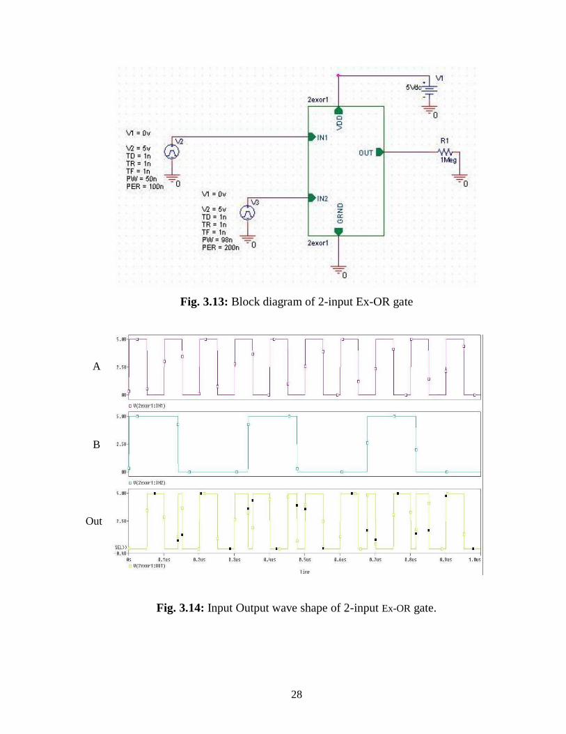
Fig. 3.13: Block diagram of 2-input Ex-OR gate
Fig. 3.14: Input Output wave shape of 2-input Ex-OR gate.
A
B
Out

29
3.4 Pass-Transistor Logic
Fig. 3.15: Basic Circuit of Pass-Transistor Logic.
Fig. 3.16: EX-NOR Gate Implemented in Pass-Transistor Logic.
Fig. 3.15 shows an EXNOR implemented in pass-transistor logic [13]. A is used as a
control signal and B is used as a pass signal. In this circuit, when A is true, B is passed to
the output. When A is false, the complement of B is passed. As can be seen this logic
form is not always active, which limits its ability to be used in long chains. The
advantage of pass-transistor logic is that it occupies much less area to construct complex
Boolean function. The EXNOR in CMOS complementary logic needs 32-input NAND

30
gates, which consisted of 12 transistors. It only need 2 transistors in pass-transistor logic
as shown in Fig. 3.15.
3.5 Comparator Design One bit Comparator design is established through a sequential process. Previously
comparator component which are developed by using Logic gates. Now the total
implemented component circuits are attached through single bit connection diagram. 3.5.1 CMOS circuit diagram of 1 Bit comparator
Fig. 3.17: CMOS circuit diagram of 1 Bit comparator

31
3.5.2 1 Bit Comparator (Gate Level Design)
Fig. 3.18: Gate level Design of 1 bit comparator
3.5.3 1 Bit Comparator (Single Block)
Fig. 3.19: Block diagram of 1 bit comparator

32
Fig. 3.20: Input Output wave shape of 1 bit comparator output
In1
In2
Out1
Out2
Out3

33
3.5.4 8-Bit Cascaded Comparator
Fig. 3.21: Block diagram of 8 Bit Cascaded Comparator

34
`
Fig. 3.22: Input Output wave shape of 8 bit comparator output
A0
A1
A2
A3
A4
A5
A6
A7
B0
B1
B2
B3
B4
B5
B6
B7
OUT1
OUT2
OUT3

35
CHAPTER 4 Layout Design of 8 Bit Cascaded Comparator
4.1 Integrated Circuit Design
The increase complexity available from Integrated Circuits [3] with passing time has
significant influence on the design of digital computer systems. Integrated Circuits
(known as chips), where an entire circuit is manufactured in a single piece of silicon,
first appeared around 1960. At that time, the chip size and transistor dimensions were
such that only a few simple gates offering primitive logic functions such as not, nand,
nor etc. could be accommodated; this level of integration is called small-scale
integration (SSI). The increasing of chip area and a progressive reducing feature size
has allowed a complexity increase of approximately one hundred every ten years.
Thus by 1970 medium scale integration (MSI) with about a thousand transistors
appeared, while by 1980 large scale integration (LSI) circuit of approximately one
hundred thousand devices were possible. At this rate, chips capable of containing

36
around ten million components were available to the designer by 1990. There is every
confidence that this projection of several million transistors per chip is realistic. This
level of integration is very large scale integration (VLSI).
4.2 Choice of Technology
Distinct types of technology are fabricated in silicon based upon the bipolar junction
transistor and the metal-oxide-semiconductor (MOS) transistor [10-13]. MOS logic
occupies a much smaller area of silicon then the equivalent bipolar logic. This is
partly due to smaller device size and partly due to the fact that MOS structure requires
fewer components. Thus MOS technology has a much higher potential packing
density. The structure of an MOS transistor is much simpler then that for bipolar
devices and this makes its manufacturing process easier. At present bipolar transistor
are faster then MOS devices. The speed of an MOS transistor is dependent upon its
size. This speed is increasing with time, owing to fabrication advances, which
continue to reduce
This surface feature size. The speed of bipolar device is dependent upon a vertical
dimension (defining the base width), which is near its limit for the fastest transistors.
The NMOS logic family is based upon n-channel MOS transistors while CMOS
requires both n-channel and p-channel MOS transistors. The NMOS process is simpler
then that for CMOS since only one transistor type is involved. NMOS logic structures
require fewer devices and occupy less area then the equivalent CMOS circuit. Despite
this CMOS is likely to be eventually the design medium for VLSI as it requires much
less power than NMOS and its circuit speed superior to that of NMOS.
4.3 The Design Approaches There are three different design approaches. These are: a) Off the self: In this approach digital design is made with chips that are available
from the manufacturers. Here the designer has no control over the chip function

37
and specification of the content of each layer manufactured in silicon. Here the
design is influence by the availability of specific function.
b) Full Custom: Here the designers have full control over the chip function
including the content of each layer manufactured in silicon. It is the most efficient
process. Here the designer's imagination is an important factor. The design can be
integrated most efficiently from the viewpoint of functionality, space and power.
1. It will take time.
2. It will result sophisticated design
3. Considerable development
4. Increasing manufacturing cost.
c) Semi Custom Design: In this approach there is a set of unconnected logic cells
already fabricated on silicon each of which can be configured to perform a Varity
of logic function. The designers only need to specify the cell interconnection and
cell configuration to provide a user define function.
4.4 The Design Process The design methodology [14] adopted for all digital design is top-down hierarchical
approach. Here the design is divided into a number of distinct levels where each level
is derived from the information in the level above it. In this way, a design progresses
from the initial system specification to its actual implementation. Thus, at each level
down in the hierarchy, the design becomes a progressively more detailed description
of how the system specification is to be implemented.
For VLSI design full custom is the best approach. The different levels in the hierarchy
for a full custom design are shown in Fig. 4.1

38
System Specification
Fig. 4.1: Top-down design hierarchies for full custom design. 4.4.1 System Design
System design is performed at the highest level. This takes the system specification
and translates it into a block diagram of the architecture. This diagram shows the
system’s functional blocks, such as cache memory, registers, arithmetic blocks, logic
blocks etc.
4.4.2 Logic Design
The next level down in the hierarchy, the architectural blocks are expended into logic
diagrams. Here each item drawn represents a particular logic function, such as gate.
Control and timing logic is also included at this level. Logic simulation can be used to
verify that the logic functions correctly and performs the tasks required by the system
specification.
System Design
Logic Design
Circuit Design
Geometric Layout
Design Rule Check
Fabrication

39
4.4.3 Circuit Design
The next level down in the in the hierarchy is the circuit design. Here the logic is
translated into circuits with dimensions assigned to the transistors. The circuit
diagrams are often drawn as stick diagrams rather than with conventional transistor
symbols. A stick diagram is a pictorial representation of the circuit in terms of the
lines and connection required at each layer of the silicon. In this level, the logic is
implemented with simple, regular transistor structure wherever possible. Circuit
simulation can verify the design at this level and provide an indication of the power
dissipation and speed. 4.4.4 Geometric Layout
If the circuit design is correct, translation to the next level down in the hierarchy can
proceed. The circuits are allocated to the positions on the silicon and geometric shapes
are generated for each silicon layer corresponding to the circuit and their
interconnections. If stick diagrams have been used then a Geometric Layout can be
derive from them by just ‘fleshing out’ their lines.
4.4.5 Design Rule Check (DRC)
The layout is checked against the circuit design to confirm that circuit details have
been correctly translated to the lower level. The layout is also checked for violations
of the fabrication process layout rules.
4.4.6 Fabrication After the layout stage, the design normally process out of the designer’s hands. The
data representation of the geometric layout is normally used to produce a mask of each
silicon layer. The masks are then used at the different production stages of the
fabrication process to produce the specified chip.

40
4.5 Layout Design Software (Microwind)
Fig. 4.2: Microwind main window
MICROWIND is licensed software. The software has been licensed in France by
Language et Informatique Inc, Toulouse, by the American Society for Engineering
Education (ASEE) in USA, and by INSA in all other countries. MICROWIND [15] is
recommended by EURO-PRACTICE, the American Society for Engineering
Education, and supported by the French Ministry of Research and Higher Education,
National Comity for Micro-Electronics Education.
The MICROWIND main window includes four main windows: the main menu, the
layout display window, the icon menu and the layer palette. The cursor appears in the
middle of the layout window and is controlled by the mouse. The layout window
features a grid that represents the current scale of the drawing, scaled in0.25 µm units
and in micron. The µm unit is fixed to half of the minimum available lithography of
the technology. The default technology is ATMEL-ES2 0.25 µm CMOS technology.

41
4.5.1 Drawing a Single MOS
The MOS symbols are reported below. The n-channel MOS is built using polysilicon
as the gate material and N+ diffusion to build the source and drain. The p-channel
MOS is built using polysilicon as the gate material and P+ diffusion to build the
source and drain.
Fig. 4.3: Symbol of nMOS & pMOS 4.5.2 Manual Design Creating a manual design of the n-channel MOS using the following procedure. The
default icon is the drawing icon shown above. It enables box editing. The display
window is empty. The palette is located in the lower right corner of the screen. A red
color indicates the current layer. Initially the selected layer in the palette is
polysilicon.
A specific command displays the characteristics of pMOS and nMOS, where the size
of the device and the process parameters can be changed very simply. By altering the
MOS model parameters and then seeing the affects on the Vds and Ids curves, it is a
good interactive tutorial on devices.
The box width should not be lower than 2, which is the minimum width of the
polysilicon box.

42
Fig. 4.4: Minimum width of polysilicon box Change the current layer into N+ diffusion by a click on the palette the Diffusion N+
button. Be sure that the red layer is now the N+ Diffusion. Draw a n-diffusion box on
the bottom of the drawing as shown below. N-diffusion boxes are represented in
green. The intersection between diffusion and polysilicon creates the channel of the
nMOS device.
4.5.3 Process Simulation Click this icon to access process simulation. The cross-section is given by a click with
the mouse at the first point and the release of the mouse at the second point. In the
example, three nodes appear in the cross-section of the n-channel MOS device: the
gate (red), the left diffusion called source (green) and the right diffusion called drain
(green), over a substrate (gray). The gate is isolated by a thin oxide called the gate
oxide. Various steps of oxidation have lead to a thick oxide on the top of the gate.
Fig. 4.5: Steps of oxidation

43
The physical properties of the source and drain are exactly the same. Theoretically,
the source is the source of channel impurities. In the case of this nMOS device, the
channel impurities are the electrons. Therefore, the source is the diffusion area with
the lowest voltage. The polysilicon gate floats over the channel, and splits the
diffusion into 2 zones, the source and drain. The gate controls the current flow from
drain to source, both ways. A high voltage on the gate attracts electrons below the
gate, creates an electron channel and enables current to flow. A low voltage disables
the channel.
4.5.4 MOS Characteristics Click the MOS characteristics icon. The screen shown below appears. It represents the
Id/Vd simulation of the nMOS device.
The MOS size (width and length of the channel situated at the intersection of the
polysilicon gate and the diffusion) has a strong influence on the value of the current.
Click OK to return to the editor. A high gate voltage (Vg =5.0) corresponds to the
highest Id/Vd curve. For Vg=0, no current flows. The maximum current is obtained
for Vg=5.0V, Vd=5.0V, with Vs=0.0.
The MOS parameters correspond to SPICE Level 3. You can alter the value of the
parameters. You may also access to Level 1. You may also skip to PMOS. Also, you
may add some measurements to fit the simulation. Finally, you can simulate devices
with other sizes in the proposed list.
4.5.5 Adding Properties for Simulation Properties must be added to the layout to activate the MOS device. The most
convenient way to operate the MOS is to apply a clock to the gate, a clock to the
source and to observe the drain. The summary of available properties is reported
below.

44
Apply a clock to the drain. Click the Clock icon, click on the left diffusion. The Clock
menu appears (See below). Change the name into « drain » and click OK. A default
clock with 3 ns period is generated. The Clock property is sent to the node and
appears at the right hand side of the desired location with the name « drain ».
Apply a clock to the gate. Click the Clock icon, click on the polysilicon gate. The
clock menu appears again. Change the name into « gate» and click OK to apply a
clock with 6 ns period. Watch the output: Click the Visible icon, click on the right
diffusion. The window below appears. Click OK. The Visible property is sent to the
node.
4.6 Designed Layout of CMOS circuits 4.6.1 Layout of the Designed inverter (NOT gate)
Fig. 4.6: Designed Layout of an Inverter (NOT gate)

45
Fig 4.6 shows the full custom design of an inverter [5] which has one pMOS and one
nMOS. Gate of the two MOS is common and named input. The source of the NMOS
is connected to the ground and source of PMOS is connected to the supply (Vdd). The
Gate of NMOS and PMOS are connected together and input is given there. Output is
taken from the point where the drain of NMOS and PMOS are connected. Dimension
of the inverter is dx=11.6 µm, dy=12.2µm.
Input output wave shape of the designed Inverter (NOT gate)
Fig. 4.7: Input output wave shape of the designed Inverter (NOT gate)
The input output wave shape of the designed inverter is shown in Fig 4.7 from the
figure it is clear that the inverter is performing well. When the input is low then the
output is high and when the input is high then the output is low. The rise time and fall

46
time of the inverter output are 270ps and 110ps respectively. The propagation delay is
190ps. By increasing the width of PMOS we can decrease the rise time of the inverter.
Simulation of the wave is completed with MOS model level 3 with 1 NMOS and 1
PMOS.
4.6.2 Layout of the Designed 3-input AND gate
Fig. 4.8: Layout of the Designed 3-input AND gate

47
Input output wave shape of the designed 3-input AND gate
Fig. 4.9: Input output wave shape of the designed 3-input AND gate
The input output wave shape of the designed 3-input and gate is shown in Fig 4.9
from the figure it is clear that the AND [1] gate is performing well. When the 3 input
is high then the output is high and when one input is low then the output is low. The
rise time and fall time of the 3 input AND Gate output are 540ps and 300ps
respectively. The propagation delay is 420ps. By increasing the width of PMOS we
can decrease the rise time of the AND gate. Simulation of the wave is complete with
MOS model level 3 with 4 NMOS, 4 PMOS.

48
4.6.5 Layout of the Designed 2-input AND gate
Fig. 4.10: Layout of the Designed 2-input AND gate

49
Input output wave shape of the designed 2-input AND gate
Fig. 4.11: Input output wave shape of the designed 2-input AND gate
The input output wave shape of the designed 2-input AND [11] gate is shown in Fig
4.11 from the figure it is clear that the AND gate is performing well. When the 2 input
is high then the output is high and when one input is low then the output is low. The
rise time and fall time of the inverter output are 500ps and 305ps respectively. The
propagation delay is 402.5ps. By increasing the width of PMOS we can decrease the

50
rise time of the AND gate. Simulation of the wave is completed with MOS model
level 3 with 3 NMOS, 3 PMOS.
4.6.7 Layout of the Designed 2-input OR gate
Fig. 4.12: Layout of the Designed 2-input OR gate

51
Input output wave shape of the designed 2-input OR gate
Fig. 4.13: Input output wave shape of the designed 2-input OR gate
The input output wave shape of the designed 2-input OR [1] gate is shown in Fig 4.13.
From the figure it is clear that the OR gate is performing well. When the one input is
high then the output is high and when both input is low then the output is low. The

52
rise time and fall time of the inverter output are 325ps and 525ps respectively. The
propagation delay is 425ps. By increasing the width of PMOS we can decreasing the
rise time of the OR gate. Simulation of the wave is complete with MOS model level 3
with 3 NMOS, 3 PMOS.
4.6.9 Layout of the Designed 2-input EX-OR gate
Fig. 4.14: Layout of the Designed 2-input EX-OR gate

53
Input output wave shape of the designed 2-input EX-OR gate
Fig. 4.15: Input output wave shape of the designed 2-input EX-OR gate
4.7 Logic Diagram of 1-bit comparator cell A[i] B[i]
A<B[i+1]
A<B[i]
A=B[i+1]
A=B[i]
A>B[i+1]
A>B[i]
Fig. 4.16: Logic Diagram of 1 bit comparator cell

54
4.8 Designed Layout of 1 bit comparator cell
Fig. 4.17: Designed Layout of 1 bit comparator cell
The designed Layout of 1 bit comparator cell is shown in Fig 4.17. It contains two NOT gate,
two 3 input AND gate, two 2 input OR gate, one 2 input AND gate, one 3 input EX-OR gate.
The size of the 1 Bit Comparator cell is 17.0µm x 18.0µm.

55
Input output wave shape of designed 1 bit comparator cell
Fig. 4.18: Input output wave shape of 1 bit comparator

56
4.9 Design layout of 8 bit comparator cell
Fig. 4.19: Designed layout of 8 bit comparator

57
Input output wave shape of designed 8 bit comparator cell
Fig. 4.20: Input output wave shape of 8 bit comparator
The full custom complete layout design of the 8-bit comparator array is shown in
Fig. 4.19. It has 8 inputs, 3 preset values & 3 outputs. Three outputs shows the value
gradually, first one is A<B, second one is A=B, Third one is A>B.
0
0
0
0
0
0
0
0
0
0
0
0
0
0
1
0
0
When A=B
0
1
0
0
1
0
0
1
1
0
1
0 1
0
0
0
0 1
When A>B
1
0
1
0
0
0

58
The full custom complete layout design of the 8-bit comparator array is shown in
Fig. 4.19. It has 8 inputs, 3 preset values & 3 outputs. Three outputs shows the value
gradually, first one is A<B, second one is A=B, Third one is A>B.
4.9 Specification of Designed Test Chip
Chip function 8 bit Comparator
Chip Size 274.8µm × 44.4µm
Chip Pins 22
No. of Transistors 128 nMOS, 128 pMOS
Technology ATMEL-ES2 5-metal 0.25µm
CMOS process
Supply Voltage 5V
Power dissipation 15.712 mW

59
CHAPTER 5 Conclusion
5.1 Conclusion In this project a 8-bit cascaded comparator has been investigated & designed using 0.25µm
CMOS Technology using Microwind 1.0 which is CMOS layout design & simulation tool,
it would be possible to use this designed circuit in a complex circuit. At first Logic Circuit
of 1-bit comparator cell has successfully implemented through ORCAD & got the correct
output result. When the simulation of 1-bit comparator gives correct result then Logic
circuit of 8-bit cascaded comparator has designed & output result is ok. Then 1-bit
comparator cell layout designed through Microwind. After getting satisfactory output result,
final 8-bit cascaded comparator layout has been designed. Now the masks are ready to use
at the different production stages of the fabrication process to produce the specified chip.
The design is mainly optimized for low power, moderate speed & less delay times. The
output 8-bit comparator along with power dissipation of 15.712 mW have been achieved.
5.2 Future Scope of Work Future scope for improvement of this project is mentioned in this section. Simulation result
shows that 8-bit comparator dissipates power of 15.712 mW. Few of design issues that limit
its performance have been discussed & various techniques can be used for its improvement
also. Such enhancements as well as the design of the improved 8-bit comparator can be
included in the future work. Since the designed 8-bit comparator delay time is 3225ps &

60
when more bit will be added, the delay time will be higher because delay time is added
consecutively from 1-bit to 8-bit. This problem may be due to the cascading techniques.
Hence improved comparator circuit need to be design to extend this work in future. Futher
scaling of technology will also led to change in calculated parameters. Hence technology
scaling can also be the future scope of this work.

61
REFERENCES [1] John P. Uyemura, Chip Design for Submicron VLSI: CMOS Layout and Simulation,
1st Edition. [2] P. Gray and R.G. Hodges, Analog Integrated Circuits, 3rd ed., John Wiley & Sons,
1993. [3] D. Hodges and H. Jackson, Analysis and Design of Digital Integrated Circuits, 2nd
Edition McGraw-Hill, 1988. [4] G. Massobrio and P. Antognetti, Semiconductor Device Modelling with SPICE, 2nd
Edition McGraw-Hill, 1993. [5] Douglas A Pucknell and kamran Eshraghian, Basic VLSI Design, 3rd Edition,
December 1998. [6] Neil H . E . Weste, Kamran Eshraghian, Principles of CMOS VLSI Design, 2nd
Edition, 2002. [7] Linda E. M. Brackenbury, Design of VLSI Systems, New Edition. [8] D. Roulston, Semiconductor Devices, McGraw-Hill, 1990. [9] S. M. Sze, Physics of Semiconductor Devices, Wiley Interscience, 1981. [10] Y. Tsividis, Operation and Modelling of the MOS Transistor, McGraw-Hill, 1987. [11] S. Wolf, Silicon Processing for the VLSI Era Volume 3: The Submicron MOSFET,
Lattice Press, 1995. [12] Floyd, Digital Fundamentals, 6th Edition. [13] Steven M. Rubin, Computer Aids for VLSI Design, 2nd Edition. [14] R. Geiger, P. Allen, and N. Strader, VLSI, Design Techniques for Analog and Digital
Circuits, McGraw-Hill, 1990. [15] N. H. E. Weste and K. Eshraghian, Principles of CMOS VLSI Design : a System
Perspective, 2nd Edition Addison-Wesley, 1993.