CIGS PV Technology: Challenges, Opportunities, and...
60
NREL is a national laboratory of the U.S. Department of Energy, Office of Energy Efficiency and Renewable Energy, operated by the Alliance for Sustainable Energy, LLC. CIGS PV Technology: Challenges, Opportunities, and Potential Rommel Noufi NCPV, NREL Date: 2/22/2013 CIGS: A High Content Technology
Transcript of CIGS PV Technology: Challenges, Opportunities, and...
NREL is a national laboratory of the U.S. Department of Energy, Office of Energy Efficiency and Renewable Energy, operated by the Alliance for Sustainable Energy, LLC.
CIGS PV Technology: Challenges, Opportunities, and Potential
Rommel Noufi NCPV, NREL Date: 2/22/2013
CIGS: A High Content Technology
Innovation for Our Energy Future
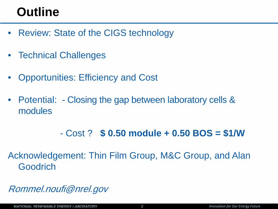
Outline • Review: State of the CIGS technology
• Technical Challenges
• Opportunities: Efficiency and Cost
• Potential: - Closing the gap between laboratory cells & modules
- Cost ? $ 0.50 module + 0.50 BOS = $1/W
Acknowledgement: Thin Film Group, M&C Group, and Alan Goodrich
2

Innovation for Our Energy Future
ZnO, ITO 2500 Å
CdS or ZnS 500 Å
Mo 0.5-1 µm
Glass, Metal Foil,
Plastics
CIGS 1-2.5 µm
CIGS Device Structure
3

Innovation for Our Energy Future
Parameters of High Efficiency CIGS Solar Cells
Sample Number Voc (V) Jsc (mA/cm2) Fill factor (%) Efficiency (%)
ZSW 0.740 35.40 77.5 20.3 ZSW
M2992-11 0.690 35.55 81.2 20.0 NREL
S2229A1-3 0.720 32.86 80.27 19.0 S2229A1-5 0.724 32.68 80.37 19.0 S2229B1-2 0.731 31.84 80.33 18.7 C3010-22-4 0.803 29.15 79.47 18.6 AIST, Monolith Flex. Module 11.60 (0.683) 34.00 68.40 16.0 (75 cm2)
EMPA, Polyimide 0.670 34.00 74.10 16.9 (18.6)
NREL, Nakada, SS 0.650 36.38 74.20 >17.5
Tolerance to wide range of molecularity
Cu/(In+Ga) 0.95 to 0.82
Ga/(In+Ga) 0.26 to 0.55
Yields device efficiency of 18% to >20%
4
Innovation for Our Energy Future
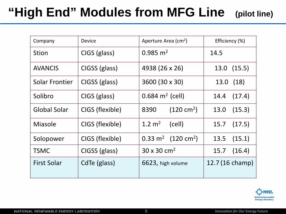
“High End” Modules from MFG Line (pilot line)
Company Device Aperture Area (cm2) Efficiency (%)
Stion CIGS (glass) 0.985 m2 14.5
AVANCIS CIGSS (glass) 4938 (26 x 26) 13.0 (15.5)
Solar Frontier CIGSS (glass) 3600 (30 x 30) 13.0 (18)
Solibro CIGS (glass) 0.684 m2 (cell) 14.4 (17.4)
Global Solar CIGS (flexible) 8390 (120 cm2) 13.0 (15.3)
Miasole CIGS (flexible) 1.2 m2 (cell) 15.7 (17.5)
Solopower CIGS (flexible) 0.33 m2 (120 cm2) 13.5 (15.1)
TSMC CIGSS (glass) 30 x 30 cm2 15.7 (16.4)
First Solar CdTe (glass) 6623, high volume 12.7 (16 champ)
5
Innovation for Our Energy Future
Technical Challenges Large impact on performance and cost
6
Innovation for Our Energy Future
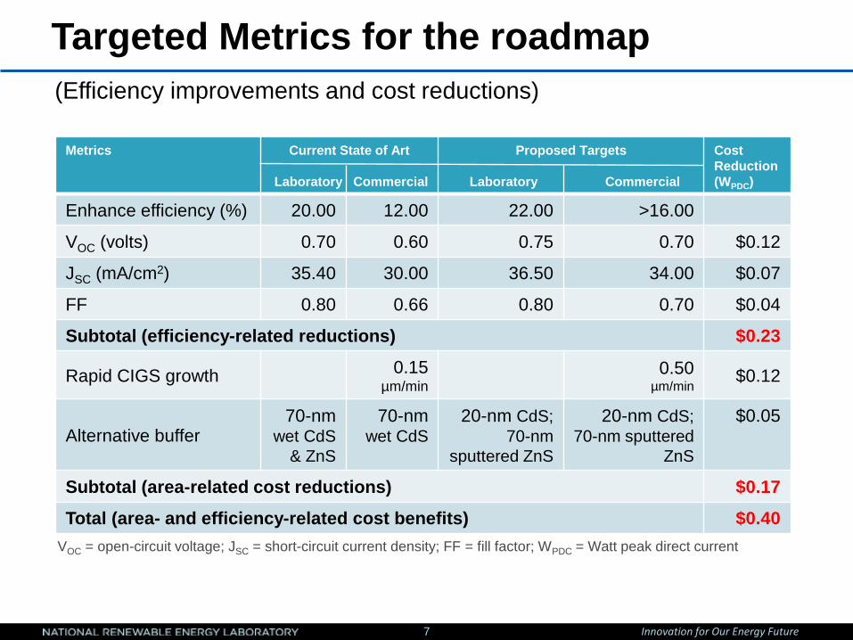
Targeted Metrics for the roadmap
7
Metrics Current State of Art
Laboratory Commercial
Proposed Targets
Laboratory Commercial
Cost Reduction (WPDC)
Enhance efficiency (%) 20.00 12.00 22.00 >16.00
VOC (volts) 0.70 0.60 0.75 0.70 $0.12
JSC (mA/cm2) 35.40 30.00 36.50 34.00 $0.07
FF 0.80 0.66 0.80 0.70 $0.04
Subtotal (efficiency-related reductions) $0.23
Rapid CIGS growth 0.15 µm/min
0.50 µm/min
$0.12
Alternative buffer 70-nm
wet CdS & ZnS
70-nm wet CdS
20-nm CdS; 70-nm
sputtered ZnS
20-nm CdS; 70-nm sputtered
ZnS
$0.05
Subtotal (area-related cost reductions) $0.17
Total (area- and efficiency-related cost benefits) $0.40
(Efficiency improvements and cost reductions)
VOC = open-circuit voltage; JSC = short-circuit current density; FF = fill factor; WPDC = Watt peak direct current

Innovation for Our Energy Future
Higher efficiency through higher photovoltage
8
Goal: Demonstrate Voc between 0.75 and 1.0 V for Ga content between 30 and 100% with efficiencies higher than the state of the art.
Relevance: Being able to maintain high efficiency (>20% as in low Ga cells) while raising the Ga content of the cell relative to In content, allows progress toward higher theoretical efficiency.
The cost reduction opportunity is about $0.12/W
Innovation for Our Energy Future
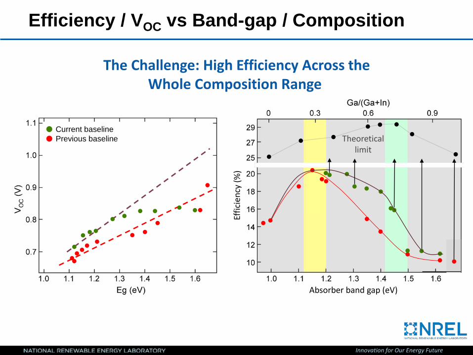
Efficiency / VOC vs Band-gap / Composition
Absorber band gap (eV)
Theoretical limit
The Challenge: High Efficiency Across the Whole Composition Range
Effic
ienc
y (%
)
Current baseline Previous baseline

Innovation for Our Energy Future
Voc is limited to a certain value

Innovation for Our Energy Future 11
Eg~1.4 eV
Eg~1.6 eV Key findings: (a) loss of collection efficiency as Ga is increased (b) Existence of random and discrete electronically inactive grains in carrier generation/collection ANALYTICAL MICROSCOPY GROUP: origin of inactive grains and/or interfaces (chemical, structural, optoelectronic studies of grains and grain boundary )
Eg~1.1 eV
•as the Ga content is increased, the overall collection of the cells decreases predominantly for the longer wavelengths (diff. length) • highest bandgap materials, such as the CuGaSe2 case, also show an overall lower collection efficiency (<90%) in the visible wavelengths, an indication additional recombination is further limiting the performance of such cells (interface recombination?)
Eg~1.2 eV
Results: EBIC/EQE

Innovation for Our Energy Future
Electronic Properties of Grain Boundaries in the Improved High-Ga CIGS Solar Cells

Innovation for Our Energy Future
Grain/Grain Boundary Structure Model
03562808-2
Cu-poor Defect Layer • A surface region (of finite thickness) including GBs exists which is Cu-deficient relative to the bulk of the grains • Cu-vacancies result in decrease in p-d repulsion. The latter causes a lowering of the EV maximum, and effectively an increase in Eg – See: Albin et al, MRS Proc., 228, p. 267, 1992; Jaffe et al, Phys. Rev. B27, 5167 (1983); B29, 1882, (1984)
– As a result, a barrier is created that repels holes from the surface and GBs.
Space charge
Neutral region
h+
Hole barrier
Mo
Cu-depleted/ inverted layer/
e--rich
p-Type core/ hole-rich
h+ e–
e–
Innovation for Our Energy Future
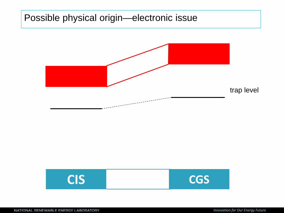
Possible physical origin—electronic issue
CIS CGS
trap level

Innovation for Our Energy Future
Previous defect calculations in CIS/CGS
S. B. Zhang et al, 1998

Innovation for Our Energy Future
CIS CGS
a) Cu vacancies are the main source of hole carrier density b) Antistie defects like neutral CuIn and InCu are the most important deep traps in CIS/CGS. c) Mcu+2 is the most important deep traps that influences the Voc of CIGS. d) Vse is not important.

Innovation for Our Energy Future
MCu + 2VCu: benefit the CIGS with Ga<50%

Innovation for Our Energy Future
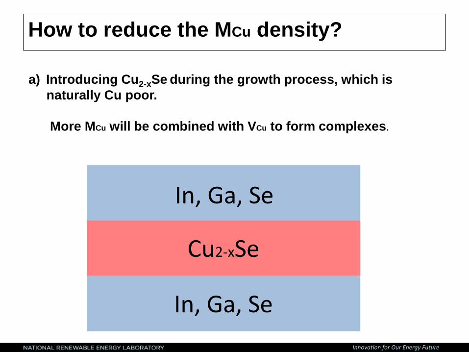
How to reduce the MCu density?
Innovation for Our Energy Future
How to reduce the MCu density?
a) Introducing Cu2-xSe during the growth process, which is naturally Cu poor. More MCu will be combined with VCu to form complexes.
In, Ga, Se
Cu2-xSe
In, Ga, Se

Innovation for Our Energy Future
b) Lower the growth temperature (e.g., grow at 450 K, work at 300 K)
CIS CGS
How to reduce the MCu density?
1) The defect density of MCu is large reduced in a large range of Cu chemical potential. 2) More growth time is needed to reach thermal equilibrium.
Innovation for Our Energy Future
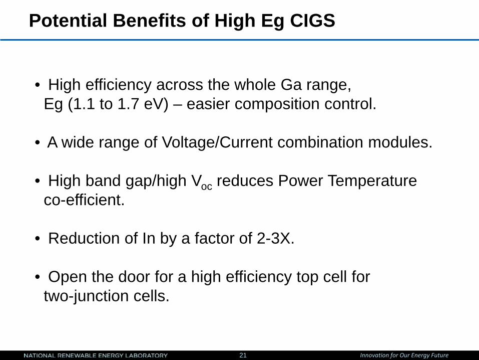
Potential Benefits of High Eg CIGS
• High efficiency across the whole Ga range, Eg (1.1 to 1.7 eV) – easier composition control.
• A wide range of Voltage/Current combination modules.
• High band gap/high Voc reduces Power Temperature
co-efficient.
• Reduction of In by a factor of 2-3X. • Open the door for a high efficiency top cell for
two-junction cells.
21

Innovation for Our Energy Future
Higher cell efficiency through higher photocurrent and lower cost through streamlined process
22
Goal: Demonstrate a >20% efficient CIGS device, using ZnOxS1-x
Relevance: The buffer/emitter layer in the CIGS device has been identified as high impact barrier for both efficiency and area related cost reduction.
Deposition methods: CBD, ALD, Sputter
The estimated cost reduction opportunity is about $0.13/W.

Innovation for Our Energy Future
Higher Cell Efficiency through Higher Photo Current
23
1. The best Jsc value obtained in the record CIGS solar cells is still quite lower than that achieved in Si (similar bandgap)
2. Great gains in efficiency could be attained if increased photocurrents are attained by maintaining Voc and FF values
3. The window materials (TCOs and CdS) are responsible for the absorption of photns that otherwise could generate additional photocurrent Best case scenario:
Potential for efficiency = 20.3% x (40.5/35.4) = 23.2%

Innovation for Our Energy Future
Design of Junction Interface with ZnOS layers
Optical Bowing in ZnOS system
Targeted range From published reports, we understand that: •Pure ZnS layer blocks the photocurrent (> 1 eV conduction band spike). •Pure ZnO layer presents a cliff and increased interface recombination. •Optimum band gap and band offset (efficiency) can be obtained by careful choice of the alloy composition.
Amorphous two-phase region
Data from sputtering, substrate temperature 200C Grimm, et. al., Thin Solid Films 520 (2011) 1330
Innovation for Our Energy Future
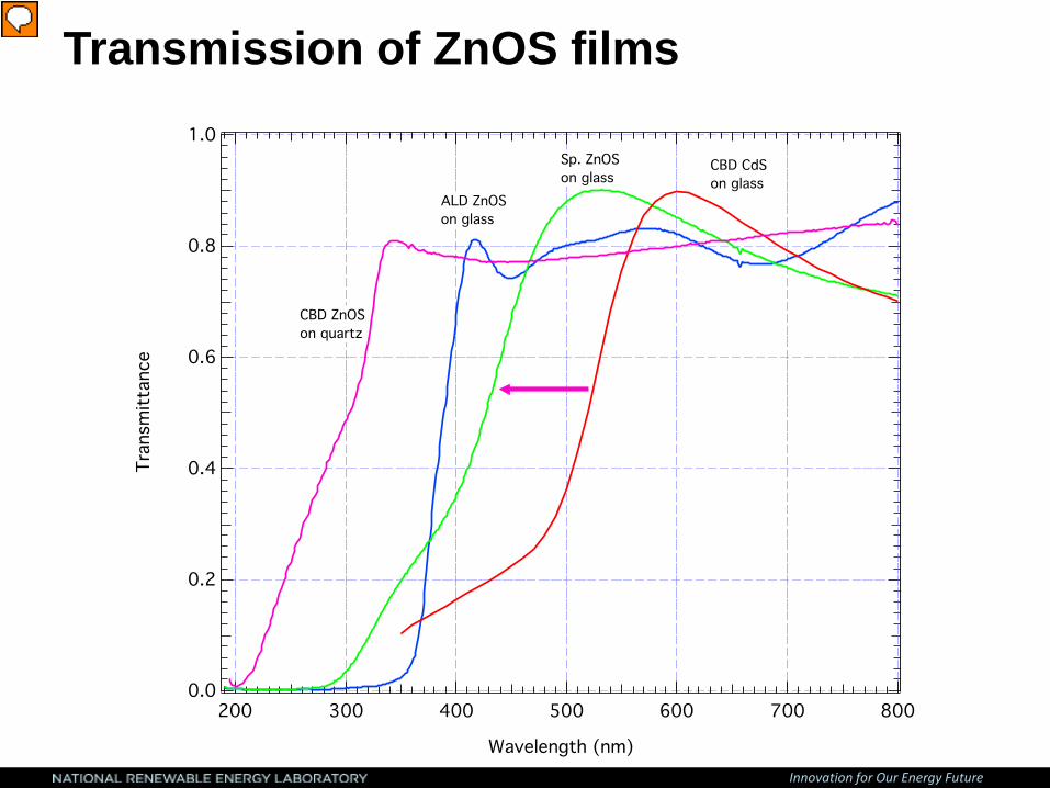
Transmission of ZnOS films
Presenter
Presentation Notes
Please note: CBD ZnS is on quartz. The optical constants measured by SE are much lower than expected. The apparent larger band gap could be due to size effect. Anyhow, the photon flux is very weak below 400 nm. ALD film is 300 nm (quite thick) Sputter ZnOS film is ~ 50 nm. Transmission curves look different because of thickness and composition differences. The takeaway is the pink arrow.

Innovation for Our Energy Future
Approach to making efficient cells using CBD ZnOS
Build on the understanding of CdS CBD model interface. o Simplify device structure, if possible o Eliminate need for long heat treatments, light soaking o Demonstrate stable, higher performing cells with higher photocurrent
Process step This work Aoyama, Japan ZSW, Germany
ZnOS thickness 20 nm 100 nm, Repeat coating 20-50 nm
Post heating None 30 min to hours 30 min to hours
Light soaking None 30 min to hours 30 min to hours
i-ZnO None None Need special ZnMgO
Best cell 18.5% 18.5% 19.0%
Comparison of our work with two leading groups
Innovation for Our Energy Future
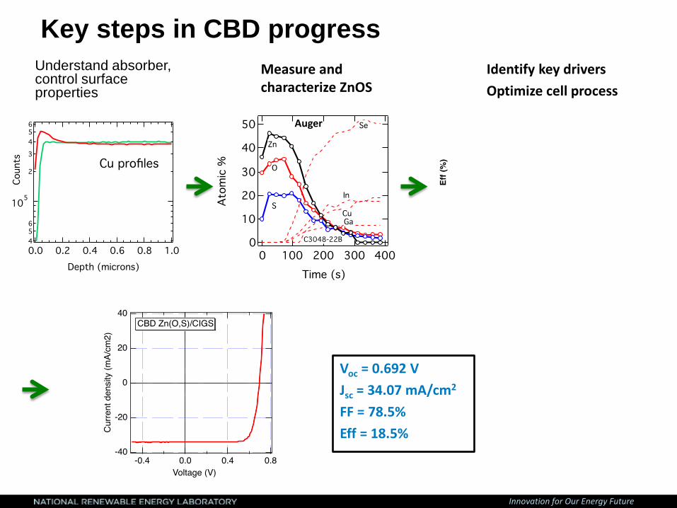
Key steps in CBD progress Understand absorber, control surface properties
Measure and characterize ZnOS
Identify key drivers Optimize cell process
Voc = 0.692 V Jsc = 34.07 mA/cm2
FF = 78.5% Eff = 18.5%
Auger

Innovation for Our Energy Future
ALD Zn(O,S) junctions Permits precise, atomic level control of composition, grading and thickness. Ideally suited for depositing coherent, covering, thin buffer layers.
Band gap variation in ZnOS films Composition
Best cell ~14.7% No AR coat
Process optimization under way. Stretch goal: demonstrate 19% without surface treatments.

Innovation for Our Energy Future
Sputter Zn(O,S) junctions Reactive sputtering of ZnS in Ar/O2
Key: Change band gap and conduction band offset with S/O ratio
Measure S/O ratio XRD
Intensity, FWHM correlate with efficiency
Optimize cell performance (sputter parameters, O2 etc)
Advanced characterization Interface: UNLV, NREL Cell: Colorado State

Innovation for Our Energy Future
Best result from sputtering
Achieved expected current gain of > 2 mA/cm2
Emitter Voc (V)
Jsc (mA/cm2)
FF(%) Eff(%)
CBD CdS C3272-21-6
0.706 31.8 78.6 17.65
Sputter ZnOS
C3272-22-6
0.666 34.3 73 16.6

Innovation for Our Energy Future
Opportunities
31

Innovation for Our Energy Future
Efficiency Opportunities - CIGS
Slide 32
Short Circuit
Current (mA/cm2)
Open Circuit Voltage
(volts/cell) Fill Factor Efficiency (%)
Practical Potential+ 30.0 - 39.0 0.75 - 0.95 0.83 25.0
Best laboratory cell 35.4 0.74 0.78 20.4
Commercial cells*
30 (32.5)
0.60 (0.69)
0.70 (0.73)
13 (15.7)
+ Ranges reflect variation in bandgap (i.e., Ga/In ratio) * Values in parentheses are from hero modules

Innovation for Our Energy Future
Future Opportunities and Challenges
33
Today Forward
ZnO, ITO (2500 Å)
• Sputter Hardened TCO
(moisture barrier) CdS (700 Å)
• Chemical Bath Deposition
• Sputter
Cd-free; dry, eliminate
CIGS (1-2.5 µm) • Multiple methods
(coevaporation, sputtering,
printing, electrodeposition)
Increase Ga-%, Reduce thickness, Rapid deposition
Uniformity (composition, temp., thickness)
Mo (0.5-1 µm) • Sputter
Na dosing
Glass, Metal Foil,
Plastics
High temp. glass Metal foils: smooth,
flex-dielectric (monolith.)
• Screen Print Ag • Reduce shadowing • Faster application
Front Contact Grid

Innovation for Our Energy Future
Pathways to increase CIGS Open Circuit Voltage from commercial (0.63 V) to best lab cell (0.80 V)
Slide 34
Action Potential Voltage
Increase (V)
Technical Risk Pathways
Improve the absorber carrier lifetime and concentration
0.05 Medium Implement in-situ quality control at minimal additional cost
Increase the Ga/In ratio in CIGS by a factor of 2 to 3
0.1 Medium Increase CIGS deposition temperature via higher temperature glass substrates or alternative stable substrates.

Innovation for Our Energy Future
Pathways to increase CIGS Short Circuit Current Density from commercial (30 mA/cm2) to best lab cell (36 mA/cm2)
Slide 35
Action
Potential Current Increase
(mA/cm2)
Technical Risk
Pathways
Reduce CdS window layer thickness
1.5 Medium Develop 20 nm thick continuous CdS layer without shunting.
Larger band gap junction partner
2.5 Medium Replace CdS (e.g. 2.5 eV) with wide bandgap emitter (i.e., ZnS (3.4 eV))
Improved TCO 1.5 Medium Develop TCO with high conductivity, transparency, environmental stability (i.e., a-InZnO)
Improved monolithic integration
1
Low Reduce line width of laser/mechanical scribing
Minimize reflection off CIG surface
1.5 Medium Develop a suitable low cost anti-reflection coating

Innovation for Our Energy Future
Pathways to increase CIGS fill factor from commercial (0.69) to best lab cell (0.82)
Action Potential
FF Increase
Technical Risk
Pathways
Reduce contact resistance
0.07 Low Improved TCO and contact grid combination
Reduce parasitic leakage current
0.10 Low Improve the density, phase, and crystallinity of the absorber

Innovation for Our Energy Future
Cost drivers per area - CIGS
Slide 37
Drivers Cost
Reduction Potential
Technical
Risk Pathways
Materials cost and availability (Indium, selenium, cadmium)
High Medium Thinner layers or replacement with Earth abundant and benign materials (e.g., CZTS, ZnS, …)
Transparent Conductors High Low ITO alternative materials and/or deposition methodologies
Glass and/or Encapsulants Medium Medium Flexible low-cost front and backsheets with low WVTR (i.e., ultrabarriers, glass replacement)
Operational costs of selenization ovens
Medium Medium Eliminate batch selenization, alternative deposition methodologies (e.g., atmospheric deposition).
Large scale spatial uniformity and improved throughput with same or lower cost of capital
High Medium Improved In-situ metrology, thermal control, and elimination of chemical bath CdS

Innovation for Our Energy Future
Potential
38
Innovation for Our Energy Future
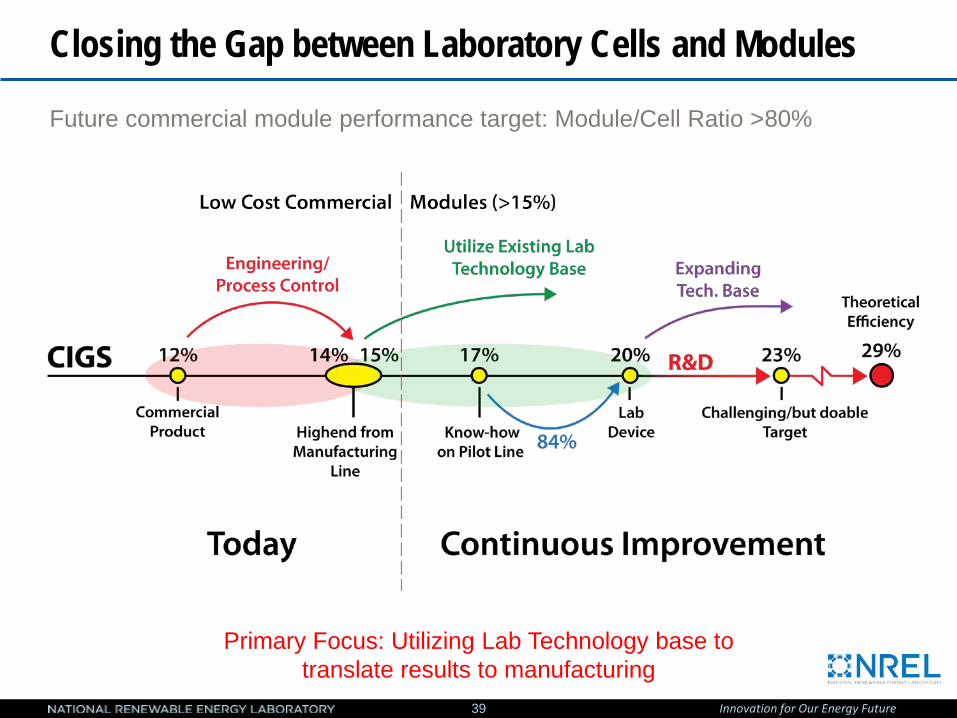
Closing the Gap between Laboratory Cells and Modules
Primary Focus: Utilizing Lab Technology base to translate results to manufacturing
Future commercial module performance target: Module/Cell Ratio >80%
39

Innovation for Our Energy Future
The Value Proposition for High Efficiency CIGS
• At no added cost ($/m2), 17.5% CIGS module = ~$0.50/Wp module ASP target • New champion lab cell efficiency (≥22%), BoS improvements are required

Innovation for Our Energy Future
END
Happy to share the presentation with you
41

Innovation for Our Energy Future
Device temperature: 25.0±1°C Device area: 0.402 cm2
Irradiance: 1000.0 W/m2
Voc = 0.67 V
Isc = 14.12 mA Jsc = 35.11 mA/cm2
Fill factor = 78.8% Imax = 13.3 mA Vmax = 0.56 V Pmax = 7.45 mW Efficiency = 18.5%
16
Voltage (V)
Cur
rent
(mA
)
12
8
4
0
-4 -0.2 0.0 0.2 0.4 0.6
X25 IV System PV Performance Characterization Team
18.5% Device using NREL’s Single Layer CBD ZnOS
Device temperature: 25.0±1°C Device area: 0.4023 cm2
Voltage bias: 0.0 V Light bias for 8.00 mA Light bias region area: 0.4023 cm2
Light bias density: 19.89 cm2
Jsc (Global) = 38.3 mA/cm2
100
Wavelength (nm)
Uns
cale
d qu
antu
m e
ffici
ency
(%)
80
60
40
20
0 400 600 800 1000 1200
Filter QE System PV Performance Characterization Team
Innovation for Our Energy Future
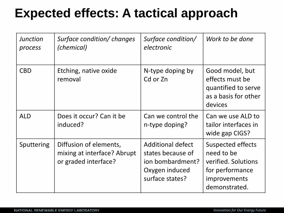
Expected effects: A tactical approach
Junction process
Surface condition/ changes (chemical)
Surface condition/ electronic
Work to be done
CBD Etching, native oxide removal
N-type doping by Cd or Zn
Good model, but effects must be quantified to serve as a basis for other devices
ALD Does it occur? Can it be induced?
Can we control the n-type doping?
Can we use ALD to tailor interfaces in wide gap CIGS?
Sputtering Diffusion of elements, mixing at interface? Abrupt or graded interface?
Additional defect states because of ion bombardment? Oxygen induced surface states?
Suspected effects need to be verified. Solutions for performance improvements demonstrated.

Innovation for Our Energy Future
Best ALD result to date
• ~ 12% cells, early stages of process development and optimization
• Need to perform loss analysis and address interface issues.

Innovation for Our Energy Future
Best result to date with sputtering
Zn(O,S) cells ~ 14 to 15% range, within 1% of CBD CdS cells. Voc loss: 50 mV, FF loss: 10 abs %.
Superior response in 400 -500 nm (CdS region) Better transmission of TCO in Zn(O,S) cell, AZO only. Red response is also good.

Innovation for Our Energy Future
Summary
We have made rapid strides in the development of ZnOS based junctions using three vastly different approaches: CBD, ALD and sputter. Process robustness and sources of variability are under investigation. Direct impact to industry expected. Focus is on the electronic properties of critical interfaces as affected by the specific process.
NREL is a national laboratory of the U.S. Department of Energy, Office of Energy Efficiency and Renewable Energy, operated by the Alliance for Sustainable Energy, LLC.
Origin of Reduced Efficiency in Cu(In,Ga)Se2 Solar Cells with High Ga Concentration
Innovation for Our Energy Future
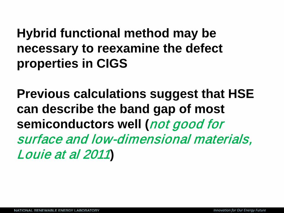
Hybrid functional method may be necessary to reexamine the defect properties in CIGS Previous calculations suggest that HSE can describe the band gap of most semiconductors well (not good for surface and low-dimensional materials, Louie at al 2011)
Innovation for Our Energy Future
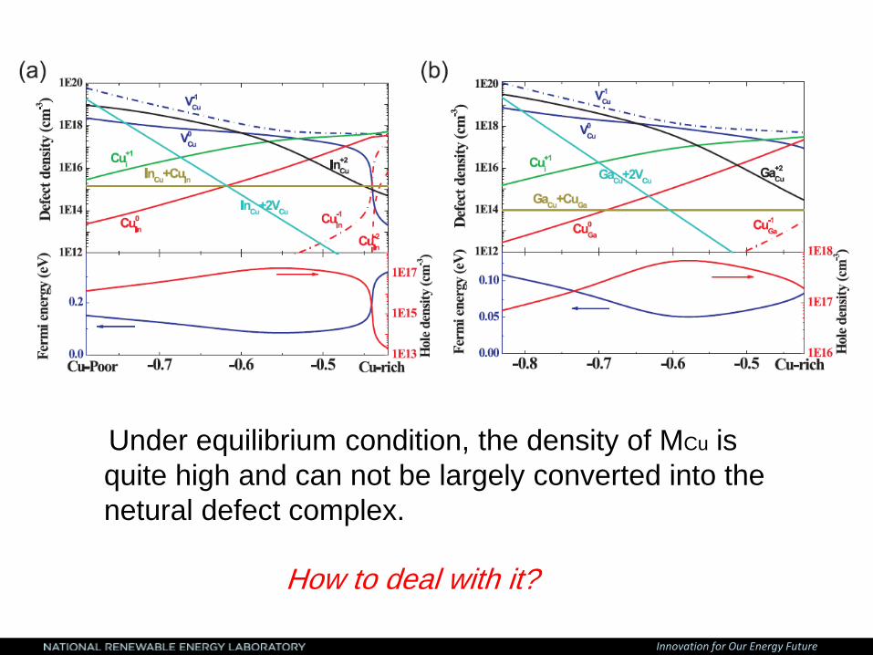
Under equilibrium condition, the density of MCu is quite high and can not be largely converted into the netural defect complex.
How to deal with it?
Innovation for Our Energy Future
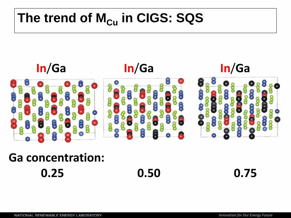
The trend of MCu in CIGS: SQS
In/Ga
Ga concentration: 0.25 0.50 0.75
In/Ga In/Ga

Innovation for Our Energy Future
The trend of Mcu in CIGS: 0/+2
The more the Ga concentration, the deeper the MCu level.
Innovation for Our Energy Future
Rapid two-step Selenization of CIGS films
52
Goal: Demonstrate the fabrication of a >20% solar cell by the two-step selenization with reaction time <10 minutes as compared to hours (practiced by industry).
Relevance: This task represents a medium cost reduction potential opportunity on area-related basis with low technical risk. The cost reduction estimate is about $24/m2 to $14/m2.

Innovation for Our Energy Future
Rapid Two-step Selenization of CIGS Films
53
1. Two typical questions are usually asked by industry. a. What is the best precursor structure and morphology for the
selenization reaction? b. What is the best selenization reaction pathway to form the CIGS
film such that the Ga profile is flat and hence the film is homogeneous?
2. To answer both interdependent questions, we propose to study the reaction pathway to rapid selenization of the Cu/In/Ga stack in Se vapor to understand the reaction diffusion kinetics, from which we can specify the conditions for thorough inter-diffusion resulting in homogeneous films.
3. The major change involves reducing the reaction time to < 10 minutes and replacing the H2Se/H2S gases with elemental Se.
Goal: Demonstrate the fabrication of a >20% solar cell by the two-step selenization with reaction time < 10 minutes
Innovation for Our Energy Future
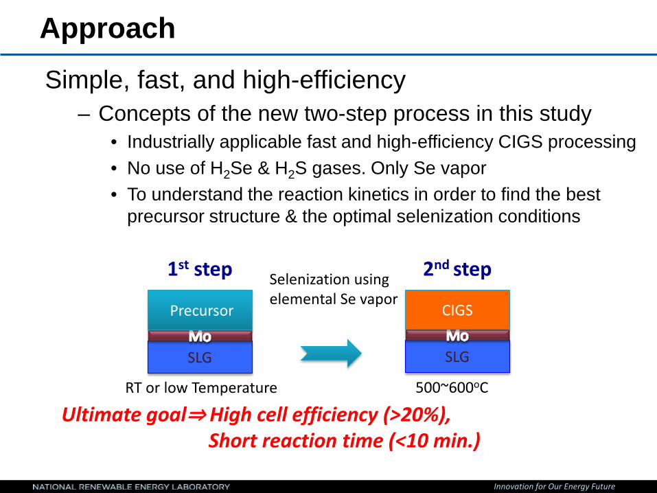
Approach Simple, fast, and high-efficiency
– Concepts of the new two-step process in this study • Industrially applicable fast and high-efficiency CIGS processing • No use of H2Se & H2S gases. Only Se vapor • To understand the reaction kinetics in order to find the best
precursor structure & the optimal selenization conditions
SLG
Precursor
SLG
CIGS
500~600oC RT or low Temperature
Selenization using elemental Se vapor
1st step 2nd step
Ultimate goal⇒ High cell efficiency (>20%), Short reaction time (<10 min.)

Innovation for Our Energy Future
Comparison of NREL and Commercial CIGS films made by two-step selenization
CIGSeS
ZnO Transform
Transform
Innovation for Our Energy Future
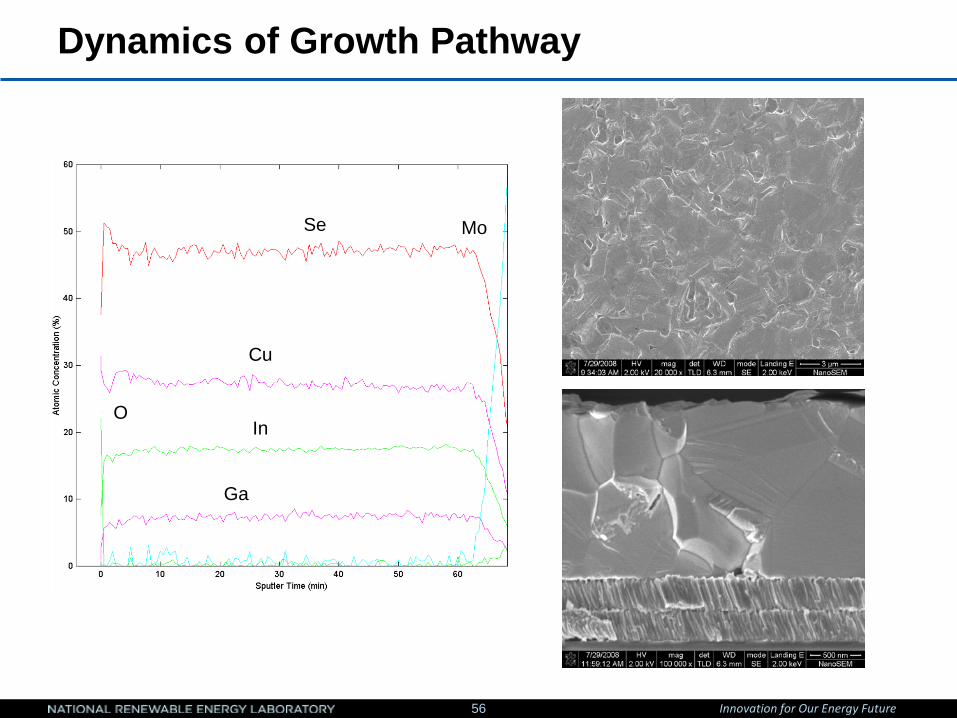
Dynamics of Growth Pathway
56
Se Mo
Cu
O In
Ga

Innovation for Our Energy Future
Dynamics of Growth Pathway
57
Voc=0.6 V, Jsc = 35.0%, FF = 72% Efficiency = 15.1%

Innovation for Our Energy Future 58
Coevaporated CIGS (on glass): Road Map
• Assumes (2011) In and Ga prices (historic highs)
Goodrich, A.; Woodhouse, M.; Noufi, R. “CIGS Road Map”. NREL Technical Report (In preparation), 2011
Presenter
Presentation Notes
Frameless 20.8 or 20.5 percent? Value of added 0.1% points at 1 TW scale.
Innovation for Our Energy Future
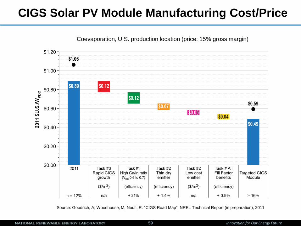
CIGS Solar PV Module Manufacturing Cost/Price
59
Coevaporation, U.S. production location (price: 15% gross margin)
Source: Goodrich, A; Woodhouse, M; Noufi, R. “CIGS Road Map”, NREL Technical Report (in preparation), 2011

Innovation for Our Energy Future
Technical Approach/past experience lessons
60
Ts~600˚C Ts~660˚C
•Deep level DAP => 0.220 eV < EA + ED < 0.280 eV •Emission decreases with increased Ts
Ts~660˚C Ts~630˚C Ts~600˚C
•Improved band-edge SR with increased Ts •Effect of Ts on SR ∆Jsc ~4 mA/cm2
OPTIMIZATION OF CuGaSe2 FOR WIDE-BANDGAP SOLAR CELLS, Miguel A. Contreras, M. Romero, and D. Young Proceedings of the 3rd World Conference in Photovoltaic Energy Conversion, Osaka, Japan 2003,
Key finding: higher (than std) processing temperatures lead to a reduction of recombination centers located deep within the gap of CGS