Chip/package co-analysis of thermo-mechanical …Chip/Package Co-Analysis of Thermo-Mechanical...
10
Chip/Package Co-Analysis of Thermo-Mechanical Stress and Reliability in TSV-based 3D ICs Moongon Jung 1 , David Z. Pan 2 , and Sung Kyu Lim 1 1 School of ECE, Georgia Institute of Technology, Atlanta, GA, USA 2 Department of ECE, University of Texas at Austin, Austin, TX, USA [email protected], [email protected], [email protected] ABSTRACT In this work, we propose a fast and accurate chip/package thermo- mechanical stress and reliability co-analysis tool for TSV-based 3D ICs. We also present a design optimization methodology to allevi- ate mechanical reliability issues in 3D IC. First, we analyze the stress induced by chip/package interconnect elements, i.e., TSV, µ-bump, and package bump. Second, we explore and validate the principle of lateral and vertical linear superposition of stress ten- sors (LVLS), considering all chip/package elements. This linear su- perposition principle is utilized to perform full-chip/package-scale stress simulations and reliability analysis. Finally, we study the mechanical reliability issues in practical 3D chip/package designs including wide-I/O and block-level 3D ICs. Categories and Subject Descriptors B.7.2 [Hardware, Integrated Circuit]: Design Aids General Terms Design Keywords 3D IC, TSV, stress, mechanical reliability, chip/package co-analysis 1. INTRODUCTION Most previous works on the thermo-mechanical stress and reli- ability of TSV-based 3D ICs have been done separately in chip or package domain. The impact of TSV-induced stress due to coef- ficient of thermal expansion (CTE) mismatch between TSV and substrate materials on device performance [1] and crack growth in TSV [7] were studied in the chip domain. As for the package domain, many works focused on the reliability of package bump (= C4 bump) [9]. Recently, authors in [8] showed the significant impact of package components on the chip domain stress. They proposed a stress exchange file to transfer the boundary conditions from package-level to silicon-level analysis. However, all of these approaches require FEA methods which are computationally ex- pensive or infeasible for full-chip or -package analysis. To overcome the limitation of FEA method, linear superposi- tion of stress tensors [5] and response surface method [4] were uti- lized. However, all of these are limited to the chip domain anal- ysis. In this paper, we propose a full-chip/package-scale thermo- mechanical stress and reliability co-analysis flow as well as a de- Permission to make digital or hard copies of all or part of this work for personal or classroom use is granted without fee provided that copies are not made or distributed for profit or commercial advantage and that copies bear this notice and the full citation on the first page. To copy otherwise, to republish, to post on servers or to redistribute to lists, requires prior specific permission and/or a fee. DAC ’12, Jun 03-07 2012, San Francisco, CA, USA Copyright 2012 ACM 978-1-4503-1199-1/12/06 ...$10.00. substrate TSV 30um device layer 30um μ-bump 20um 20um TSV Pkg-bump 30um 100um 100um TSV Pkg-bump 30um 100um μ-bump 20um 100um BEOL Back metal 5um (a) (b) (c) (d) underfill underfill TSV Pkg-bump device layer top substrate surface BEOL μ-bump TSV Back metal (e) (f) Figure 1: Impact of bumps and underfill on the stress of device layer (= red line). (a) TSV only [5] (b) TSV + µ-bump (c) TSV + package-bump (d) TSV + µ-bump + package-bump. (e) De- formed structure of (b). (f) Deformed structure of (c). Both (e) and (f) are drawn with 10X deformation scale factor. sign optimization methodology to reduce the mechanical reliability problems in TSV-based 3D ICs. We show the impact of design parameters such as the size and pitch of chip/package interconnect elements and the number of dies in the stack on thermo-mechanical stress and reliability. The main contributions of this work include the following: (1) Modeling: Compared with existing works, we simulate more de- tailed 3D IC structures including both chip and package compo- nents and study their interaction and impact on thermo-mechanical stress and reliability. (2) Full-chip/package co-analysis: We, for the first time, validate the principle of lateral and vertical linear superposition of stress tensors induced by each chip/package inter- connect element such as TSV, µ-bump, and package-bump against FEA simulations. We apply this methodology to generate a stress map and a reliability metric map in full-chip scale. (3) Case study: we study the mechanical stress and reliability issues in practical 3D chip/package designs including wide-I/O and block-level 3D ICs. 1 2. MOTIVATION We first examine how various chip/package interconnect compo- nents interact and alter the thermo-mechanical stress distribution on the device layer around TSV caused by the CTE mismatch between 1 We also explore the impact of TSV/bump placement, size, and pitch on the overall system, and the materials are moved to the Supplemental Section due to the space limit. 317
Transcript of Chip/package co-analysis of thermo-mechanical …Chip/Package Co-Analysis of Thermo-Mechanical...
Chip/Package Co-Analysis of Thermo-Mechanical Stressand Reliability in TSV-based 3D ICs
Moongon Jung1, David Z. Pan2, and Sung Kyu Lim1
1 School of ECE, Georgia Institute of Technology, Atlanta, GA, USA2 Department of ECE, University of Texas at Austin, Austin, TX, [email protected], [email protected], [email protected]
ABSTRACTIn this work, we propose a fast and accurate chip/package thermo-mechanical stress and reliability co-analysis tool for TSV-based 3DICs. We also present a design optimization methodology to allevi-ate mechanical reliability issues in 3D IC. First, we analyze thestress induced by chip/package interconnect elements, i.e., TSV,µ-bump, and package bump. Second, we explore and validate theprinciple of lateral and vertical linear superposition of stress ten-sors (LVLS), considering all chip/package elements. This linear su-perposition principle is utilized to perform full-chip/package-scalestress simulations and reliability analysis. Finally, we study themechanical reliability issues in practical 3D chip/package designsincluding wide-I/O and block-level 3D ICs.
Categories and Subject DescriptorsB.7.2 [Hardware, Integrated Circuit]: Design Aids
General TermsDesign
Keywords3D IC, TSV, stress, mechanical reliability, chip/package co-analysis
1. INTRODUCTIONMost previous works on the thermo-mechanical stress and reli-
ability of TSV-based 3D ICs have been done separately in chip orpackage domain. The impact of TSV-induced stress due to coef-ficient of thermal expansion (CTE) mismatch between TSV andsubstrate materials on device performance [1] and crack growthin TSV [7] were studied in the chip domain. As for the packagedomain, many works focused on the reliability of package bump(= C4 bump) [9]. Recently, authors in [8] showed the significantimpact of package components on the chip domain stress. Theyproposed a stress exchange file to transfer the boundary conditionsfrom package-level to silicon-level analysis. However, all of theseapproaches require FEA methods which are computationally ex-pensive or infeasible for full-chip or -package analysis.
To overcome the limitation of FEA method, linear superposi-tion of stress tensors [5] and response surface method [4] were uti-lized. However, all of these are limited to the chip domain anal-ysis. In this paper, we propose a full-chip/package-scale thermo-mechanical stress and reliability co-analysis flow as well as a de-
Permission to make digital or hard copies of all or part of this work forpersonal or classroom use is granted without fee provided that copies arenot made or distributed for profit or commercial advantage and that copiesbear this notice and the full citation on the first page. To copy otherwise, torepublish, to post on servers or to redistribute to lists, requires prior specificpermission and/or a fee.DAC ’12, Jun 03-07 2012, San Francisco, CA, USACopyright 2012 ACM 978-1-4503-1199-1/12/06 ...$10.00.
substrate TSV 30um
device layer
30um
μ-bump 20um
20um
TSV
Pkg-bump
30um
100um
100um
TSV
Pkg-bump
30um
100um
μ-bump 20um
100um
BEOL
Back metal 5um
(a) (b)
(c) (d)
underfill
underfill
TSV
Pkg-bumpdevice layer
top substrate surface BEOLμ-bump
TSV
Back metal
(e) (f)
Figure 1: Impact of bumps and underfill on the stress of devicelayer (= red line). (a) TSV only [5] (b) TSV + µ-bump (c) TSV+ package-bump (d) TSV + µ-bump + package-bump. (e) De-formed structure of (b). (f) Deformed structure of (c). Both (e)and (f) are drawn with 10X deformation scale factor.
sign optimization methodology to reduce the mechanical reliabilityproblems in TSV-based 3D ICs. We show the impact of designparameters such as the size and pitch of chip/package interconnectelements and the number of dies in the stack on thermo-mechanicalstress and reliability.
The main contributions of this work include the following: (1)Modeling: Compared with existing works, we simulate more de-tailed 3D IC structures including both chip and package compo-nents and study their interaction and impact on thermo-mechanicalstress and reliability. (2) Full-chip/package co-analysis: We, forthe first time, validate the principle of lateral and vertical linearsuperposition of stress tensors induced by each chip/package inter-connect element such as TSV, µ-bump, and package-bump againstFEA simulations. We apply this methodology to generate a stressmap and a reliability metric map in full-chip scale. (3) Case study:we study the mechanical stress and reliability issues in practical 3Dchip/package designs including wide-I/O and block-level 3D ICs.1
2. MOTIVATIONWe first examine how various chip/package interconnect compo-
nents interact and alter the thermo-mechanical stress distribution onthe device layer around TSV caused by the CTE mismatch between1We also explore the impact of TSV/bump placement, size, and pitch on theoverall system, and the materials are moved to the Supplemental Sectiondue to the space limit.
317

TSV
Figure 2: Impact of package components on the stress (σrr)around TSV on device layer (FEA results).
Pkg-bump
Figure 3: Comparison of impact of package-bump on the de-vice layer stress (σrr) between 2D IC and 3D IC (2-die stack)(FEA results).
TSV and substrate materials. First, we only consider TSV and sub-strate which most previous works studied. We employ the samesimulation structure used in [5] as shown in Figure 1(a). Then,we add a µ-bump and underfill layer above the substrate as shownin Figure 1(b). All structures undergo ∆T = -250◦C of thermalload (annealing/reflow 275◦C→ room temperature 25◦C). As Fig-ure 2 shows, by adding the µ-bump layer (= dotted red line), wesee slightly more tensile (= positive) stress than the TSV-only case(= solid black line). This is because ∆CTE of µ-bump and under-fill is 24 ppm/K, while that of TSV and substrate is 14.7 ppm/K,hence the deformation of the entire structure is largely determinedby the µ-bump and underfill layer. Since the top side of µ-bumplayer is free surface, the entire structure easily bends upward asall the elements shrink from the negative thermal load as shown inFigure 1(e). Thus, the materials on device layer stretch outward,which results in more tensile stress.
On the other hand, if we add a package-bump (= C4 bump) layerbelow the substrate as shown in Figure 1(c), now the entire structurebends downward as shown in Figure 1(f) because package elementsare shrinking more than chip elements. The ∆CTE of packagebump and underfill is 22 ppm/K. This generates highly compressive(= negative) stress on the device layer. Comparing Figure 1(b) andFigure 1(c), we see that the bending direction depends on whichlayer shrinks more: in both cases, the bump layers shrink morethan the silicon substrate.
Lastly, we include both bump layers as shown in Figure 1(d).In this case, the ∆CTE is almost the same (24 ppm/K on the top,22 ppm/K on the bottom). However, the overall structure bendsdown in a similar fashion as shown in Figure 1(f) because of thesheer volume of package bump layer (= shrinking more than theµ-bump layer). This in turn causes compressive stress in the de-vice layer. However, the magnitude is slightly more (= solid greenline in Figure 2) than the package-bump layer only case (= dottedblue line). One might expect the overall compressive stress would
die0
μ-bump
TSV
die1
die0
die1
die2
die3
Pkg-bump
Pkg-substrate
750um
20um
30um
100um
1000um
device layer
(a) (b)
BEOL
Back metal
BEOL
underfill
Figure 4: Side view of baseline chip/package simulation struc-tures. (a) 2-die stack (b) 4-die stack.
be less because the µ-bump layer tries to bend upward while thepackage-bump layer tries to bend downward (= canceling effect).However, this additive effect is because the µ-bump layer eventu-ally bends down and adds more compressive stress to the devicelayer. Remember that the bending direction of the µ-bump layeris affected by adjacent layers. Since now the deformation of theentire structure is dominated by the package-bump layer, the flexi-ble underfill material in the µ-bump layer easily bends downward.These basic simulations clearly show the importance of consideringpackage element impact on the chip-domain stress distribution.
Figure 3 shows the stress contributions of package bump and un-derfill layer to the chips (2D vs. 3D) mounted on it. For the 3DIC/package structure, we build a two-die stack chip/package struc-ture similar to Figure 4(a) excluding TSV and µ-bump. This wasto examine the impact of package-bump solely. The bottom die (=die0) is thinned, and we examine the device layer of this thin die.One 2D IC/package structure is also created, where we use a singleun-thinned die of 1000 µm thickness. We examine the device layerof this un-thinned die. We apply the same thermal load (∆T = -250◦C) for both cases. Figure 3 shows that the 3D IC experiencesmore severe compressive stress than the 2D IC case. The main rea-son is the thickness and the flexibility of the die that we are moni-toring. Even though the thickness of the entire structure is thickerin 3D IC, the thin die (30 µm thick) and the underfill material abovethe thin die is much more flexible than the un-thinned substrate in2D IC. Thus, this thin die is highly affected by the package-bumpunderneath it. This indicates that the impact of package-bump ismore significant in 3D IC.
3. 3D IC/PACKAGE STRESS MODELINGWe use the von Mises yield criterion [10] as a mechanical relia-
bility metric for TSVs, which is explained in Section S.1. However,we do not use a specific threshold value for the von Mises criterionin this work, since it is greatly affected by fabrication process.
3.1 3D IC/Package Simulation StructureFigure 4 shows our simulation structure, where the dimensions
of our baseline simulation structures are based on the fabricatedand/or published data [2, 8]. In this work, we specifically exam-ine the stress distribution on device layer for each die shown inred lines in Figure 4. Our baseline TSV diameter, height, land-ing pad size, Cu diffusion barrier thickness, and dielectric linerthickness are 5 µm, 30 µm, 6 µm, 50 nm, and 125 nm, respec-tively. We use Ti and SiO2 as Cu diffusion barrier and liner mate-rials. Also, diameter/height of µ-bump and package-bump are 20µm and 100 µm, respectively, unless otherwise specified. Materialproperties used for our experiments are as follows: CTE (ppm/K) /Young’s modulus (GPa) for Cu = (17/110), Si = (2.3/188), SiO2 =
318

(a)
(b)
TSV
TSV
Figure 5: Impact of die stacking on device layer stress (FEAresults). (a) σrr stress on device layer in each die in 4-die stack.(b) von Mises stress in each die in a 4-die stack.
(0.5/71), Ti = (8.6/116), package-bump (SnCu)= (22/44.4), µ-bump(Sn97Ag3) = (20/26.2), underfill = (44/5.6), package substrate (FR-4) = (17.6/19.7).
We use a FEA simulation tool ABAQUS to perform experiments,and all materials are assumed to be linear elastic and isotropic. Wealso discuss the impact of the anisotropic Si material property onthe thermo-mechanical stress and reliability in Section S.4. Theentire structure undergoes ∆T = -250◦C of thermal load (anneal-ing/reflow 275◦C→ room temperature 25◦C) to represent a fabri-cation process. In addition, all materials are assumed to be stressfree at the annealing/reflow temperature.
3.2 Impact of Die StackingPrevious works on the full-chip thermo-mechanical stress analy-
sis used the same stress pattern for different dies in a multiple-diestack [1, 5]. In this section, for the first time, we examine how thethermo-mechanical stress distribution on the device layer aroundTSV differs across strata. We employ the four-die stack structurefor this purpose. Also, we use only one TSV, µ-bump, and package-bump for each die or layer, respectively, and their center locationsare aligned as shown in Figure 4.
First of all, the stress level, the extent of compression or tension,differs significantly across dies as shown in Figure 5(a). The overallstress trend remains similar: the stress is highest at TSV edge anddecays then saturates as distance increases from the TSV center.However, the bottom-most die (= die0, solid red line), which isclosest to the package-bump layer, shows most compressive stressamong three dies containing TSV. This is because the impact ofpackage-bump is most significant in die0 due to their proximity.
Also, as we go to the upper dies, the stress level becomes closerto the case considering only TSV and substrate. We also see that thestress curve of die0 is very close to the case of TSV + µ-bump +package-bump (= dotted purple line), which does not contain thepackage substrate and un-thinned top die shown in Figure 1(d).This also indicates that the stress level in die0 is mostly determinedby package-bump. The stress distribution in die3 (un-thinned top
Figure 7: Vertical linear superposition of σrr stress in a 2-diestack shown in Figure 6
die without TSVs) is almost flat (-110 ± 5 MPa). Since die3 doesnot contain any TSVs, there is no local von Mises stress peak (=dangerous region) caused by TSVs. Thus, we only consider thedies containing TSVs in this work.
Moreover, we observe that the mechanical reliability problemis most severe in die0 shown in Figure 5(b). The maximum vonMises stress at TSV edge in die0 is about 110 MPa higher than theupper two dies. This is again mostly due to the package-bump thatinduces large deformation at the nearest die.
4. HANDLING FULL-CHIP/PACKAGEFEA simulation for multiple TSVs, µ-bumps, and package-bumps
require huge computing resources and time, thus it is not feasi-ble for a full-system-scale analysis. In this section, we presenta chip/package thermo-mechanical stress co-analysis flow in full-chip/package scale. We use the principle of lateral and vertical lin-ear superposition of stress tensors from individual TSVs, µ-bumps,and package-bumps to enable a full-system-level analysis. We vali-date our approach against FEA simulation results. Based on the lin-ear superposition method, we build full-chip stress maps and thencompute the von Mises yield metric to assess the mechanical relia-bility problems in TSV-based 3D ICs.
4.1 Lateral and Vertical Linear SuperpositionIn [5], authors used the principle of linear superposition of stress
tensors to perform a full-chip stress and reliability analysis consid-ering many TSVs. In that case, all stress contributors (= TSVs) areon the same layer, hence we call this lateral linear superposition.However, as we consider the impact of µ-bump and package-bump,which are not in the same layer where TSVs are located, this laterallinear superposition cannot be used alone. Fortunately, the princi-ple of linear superposition is not limited to 2D plane, but applicableto any linearly elastic structures including 3D structures.
Figure 6 illustrates our vertical linear superposition method, whichenables us to consider the stress induced by elements which are notin the same layer. We first decompose the target structure into fourseparate structures: TSV only, package-bump only, µ-bump only,and background which does not contain TSV and bumps. Next, weobtain stress tensors along the red line on device layer affected byeach interconnect element separately from FEA simulations. Then,we add up the stress tensors from TSV only, package-bump only,and µ-bump only structures, and subtract twice the magnitude ofthe background stress tensors since this background stress is al-ready included in previous three structures. If the point under con-sideration is affected by n components, then we need to substractn-1 times the background stress.
Figure 7 shows the stress distributions from each structure aswell as the stress obtained by the vertical linear superposition. Wesee that µ-bump induces more tensile stress than background andpackage-bump generates much more compressive stress than back-ground, which is discussed in Section 2. We also observe that evenwithout interconnect elements (= background) device layer is in
319

μ-bump
TSV
Pkg-bump
die0
die1
Pkg-substrate
TSV
Pkg-bump
μ-bump
= + + ‒ 2x
target TSV only pkg-bump only μ-bump only background
Figure 6: Illustration of vertical linear superposition with a 2-die stack structure. Stress is extracted along the red line on devicelayer from each structure using FEA tool.
compression due to the shrinking of the underfill material whichhas the highest CTE (= 44 ppm/K) among all materials in the simu-lation structure. Most importantly, our vertical linear superpositionmethod matches well with the target stress distribution. Althoughwe see the maximum error (11 MPa) occurs inside TSV, this isinevitable since we ignore the direct vertical interaction betweenTSV, µ-bump, and package-bump by decomposing the structure.Nonetheless, this error is acceptable for a fast full-system-scaleanalysis.
To obtain the stress tensor at a point affected by multiple TSVs,µ-bumps, and package-bumps, we apply both lateral and verticallinear superposition (LVLS) as follows:
S =
nTSV∑i=1
STSV i +
nµB∑j=1
SµBj +
npkgB∑k=1
SpkgBk
−(nTSV + nµB + npkgB − 1)× Sbg (1)
where, S is the total stress at the point under consideration andSTSV i, SµBj , and SpkgBk are individual stress tensor at this pointdue to ith TSV, jth µ-bump, and kth package-bump, respectively.Sbg indicates the background stress at that point.
4.2 Full-Chip/Package Stress Analysis FlowWe briefly explain how we perform a full-chip/package stress
analysis based on the LVLS method. We first build a stress libraryfrom FEA simulations. This library contains stress tensors along anarbitrary radial line on the device layer induced by each intercon-nect element, i.e., TSV, µ-bump, and package-bump, separately.Given locations of TSVs, µ-bumps, and package-bumps, we finda stress influence zone for each element. Beyound this stress in-fluence zone of each interconnect element, the stress induced bythe element under consideration is negligible [5]. In our work, weuse five times the diameter of each component as a stress influencezone, where stress level is saturated to the background stress levelfrom FEA simulations.
Then, we associate each grid point with all the interconnect el-ements whose stress influence zone overlaps with the point. Next,we apply the LVLS method at the point under consideration to ob-tain the stress tensor induced by every component found in the as-sociation step. Finally, we compute the von Mises stress to assessthe mechanical reliability problem in TSVs. More details of ouralgorithm is discussed in Section S.6.
4.3 Validation of LVLSIn this section, we validate our LVLS method against FEA sim-
ulations by varying the number of TSVs, µ-bumps, and package-bumps as well as their arrangement. We set the minimum pitch ofTSV, µ-bump, and package-bump as 10 µm, 20 µm, and 200 µmfor all test cases. Stress tensors along the radial line on device layerinduced by each interconnect element (stress tensor library) are ob-tained through FEA simulation with 0.25 µm interval. In our lin-ear superposition method, simulation area is divided into uniformarray style grid with 0.1 µm pitch. If the stress tensor at the grid
Table 1: Von Mises stress comparison between FEA and LVLSfor a 4-die stack structure (die0). Error = LVLS - FEA. (AtTSV edge, typical von Mises stress level is around 900 MPa.)# TSV FEA LVLS max error (MPa)
/µ-B# node run
# grid run inside TSV outside/pkg-B time time TSV edge TSV1/1/1 754K 1d2h 1M 23s -11.4 -12.6 7.92/2/1 812K 1d2h 1M 26s -12.7 -13.2 7.35/5/2 902K 1d6h 6M 2m43s -14.1 -15.3 8.2
10/10/4 1.3M 1d20h 9M 6m44s -23.1 -19.8 9.410/10/9 1.4M 2d0h 16.8M 11m11s -22.5 -20.5 11.9
point under consideration is not obtainable directly from the stresslibrary, we compute the stress tensor using linear interpolation withadjacent stress tensors in the library.
Table 1 shows some of our comparisons in die0 in a four-diestack, which shows the largest errors among three dies containingTSVs due to its proximity to package-bumps. Also, we only list thecases with the minimum pitches for each component, which againshows maximum errors. First, we observe a huge run time reduc-tion in our LVLS method. Note that we perform FEA simulationsusing 8 CPUs while only one CPU is used for our linear super-position method. Even though the LVLS method performs stressanalysis on a 2D plane (= device layer), whereas FEA simulation isperformed on the entire 3D structure, we can perform stress analy-sis for other planes in a similar way if needed.
The error between FEA simulations and LVLS is very small.Results show that our LVLS method underestimates stress mag-nitude inside TSV and TSV edge, and overestimates outside TSV,as shown in Figure 7. In general, the most critical region for themechanical reliability is the interface between different materials,hence TSV edge is most important in our case. Even though themaximum error at TSV edge is as high as -20.5 MPa, its % erroris only -2.24 %. Figure 8 shows one test case comparison of vonMises stress between FEA and LVLS. The structure has 10 TSVs(5 µm diameter and 10 µm pitch), 10 µ-bumps (20 µm diameterand 40 µm pitch), and 9 package-bumps (100 µm diameter and200 µm pitch). It clearly shows our LVLS method matches wellwith the FEA simulation result.
5. SIMULATION RESULTSWe implement a chip/package thermo-mechanical stress and re-
liability co-analysis flow based on LVLS in C++/STL. More detailscan be found in Section S.6. We explore the impact of package-bump and µ-bump on the reliability in full-system scale. Also,we examine the reliability concerns in wide-I/O DRAM and block-level 3D IC designs.
In our experiments, we adopt a regular TSV placement style inwhich TSVs are placed uniformly across each die or inside TSVblocks with pre-defined pitch. In all cases, the pair of TSV and µ-bump is vertically aligned. Default diameter/height (µm) of TSV,µ-bump, and package-bump are 5/30, 10/10, and 100/100, respec-
320

(a) (b) (c)
TSV TSV TSV TSV
LVLS
FEA200um
40um
Pkg-bump
μ-bump
TSV
Figure 8: Sample stress comparison between FEA and LVLS. (a) Test structure. (b) Close-up shot of von Mises stress map (usingLVLS) taken from the red box in (a) on the device layer in die0 in a 4-die stack. (c) FEA vs. LVLS along the red line in (b).
die w/o pkg die0 w/ pkg
die1 w/ pkg die2 w/ pkg
(a) (b)
(c) (d)
Figure 9: Impact of package components and die stacking onthe mechanical reliability of TSVs (900 TSVs in each die).
tively, unless otherwise specified.
5.1 Impact of Package-Bump and µ-BumpWe first study the impact of package-bump and µ-bump on the
mechanical reliability of different dies in a four-die stack. We alsocompare this to the case without these components as in the pre-vious work [5] as shown in Figure 1(a). In this experiment, thepitch of TSV/µ-bump and package-bump are 20 µm and 100 µm,respectively; the total number of TSV/µ-bump and package-bumpare 900 and 16, respectively, as shown in Figure 10(a).
We first observe that unlike the die without package-bumps andµ-bumps (Figure 9(a)) and the upper dies with package compo-nents (Figure 9(c) and (d)), TSVs in die0 (Figure 9(b)) experiencelarge variations of von Mises stress across the die. This is be-cause die0 is highly affected by package-bumps underneath it, andhence depending on the relative position between TSVs in die0 andpackage-bumps the von Mises stresses of TSVs change noticeably.2
We also identify that higher von Mises stress occurs around package-bump edge and in between package-bumps due to constructive stressinterference shown in Figure 10(b). However, as we see in the
2Note that we see higher von Mises stress level in (Figure 9(a) than theprevious work [5] even with the same simulation structure. This is becausewe use the Young’s modulus of 188 GPa for Si instead of 130 GPa in [5] asa worst case scenario. More details are discussed in Section S.4.
Pkg-bump 200um
stress
(MPa)
780
810
840
870
900
930
960
750
(a) (b)
Figure 10: Von Mises stress map for TSVs (die0 in a 4-diestack). Colored dots are TSVs and white circles are package-bumps. (a) Test structure. (b) Close-up shot of red box in (a)
Table 2: Reliability in wide-I/O DRAM.case von Mises stress distribution (MPa) median
780-810 810-840 840-870 870-900 900-930 (MPa)(a) 30 114 52 220 608 944.8(b) 182 842 0 0 0 856.2
center of Figure 10(b), if the distance between TSV and package-bumps is long enough, the von Mises stress of TSV becomes low.
Interestingly, die1 shows lowest von Mises stress level among allcases even though die2 is farthest from package-bumps. This is dueto the fact that die2 is affected by the rigid un-thinned top siliconsubstrate above it. Since die0 is most problematic in terms of themechanical reliability, we only consider die0 in a four-die stack inthe subsequent experiments.
5.2 Case Study I: Wide-I/O DRAMWide-I/O based 3D DRAM is fast becoming the first mainstream
product that utilizes TSV in 3D ICs, mainly targeting mobile com-puting applications such as smart phones which need lower powerconsumption and high data bandwidth. In this section, we evaluatethe reliability concerns of TSVs in wide-I/O DRAM. We follow theTSV placement style similar to the work in [6], where TSV arraysare placed in the middle of a chip. We assume that 2x128 TSV ar-ray (per memory bank) is placed in the middle of a chip shown inFigure 11. We employ four memory banks and 1024 TSVs in to-tal. We set the pitch of TSV/µ-bump and package-bump as 15 µmand 200 µm, respectively. We compare two cases; (a) Package-bumps are placed right underneath TSV arrays; (b) Package-bumpsare placed with 200 µm spacing from TSV arrays. This 200 µmdistance is chosen since we see that the effect of package-bump onthe TSV reliability is negligible beyond 200 µm in case of the 100µm diameter package-bump shown in Figure 16.
Table 2 clearly shows that the chip/package co-design can greatlyreduce the mechanical reliability concerns in TSV-based 3D ICs.
321

8mm8
mm
Bank0 Bank1
Bank2 Bank3
2x128 TSV array
Bank0 Bank1
Bank2 Bank3
(a) (b)
Pkg-bump
200um
… …
… …
… …
… …
Figure 11: Mechanical reliability in wide I/O DRAM. 1024TSVs are placed in the middle of a chip. (a) Package-bumps areplaced underneath TSV arrays. (b) Package-bumps are placed200 µm apart from TSV arrays. (not drawn in scale.)
(a) (b)
1000um
1200um
Pkg-bump
200um
14 15 161 2
3
4 5 6
7 89
10
12
13 14
11
15
16
Pkg-bump
200um
4 5 6
Figure 12: Mechanical reliability in block-level 3D IC. (a) Sam-ple layout of block-level design. (b) Von Mises stress map forTSVs in red box in (a).
With a safe margin of 200 µm (= case(b)), von Mises stress magni-tude reduces significantly. Thus, given the TSV placement, we canfind safe locations for package-bumps without affecting the pack-age design much, or vice versa.
5.3 Case Study II: Block-Level 3D ICIn this section, we study the reliability issues in block-level 3D
designs. 3D block-level designs are generated using an in-house3D floorplanner which treats a group of TSVs as a block shown inFigure 12. Total 16 TSV blocks (368 TSVs) are used and the TSVpitch is 15 µm. Package-bumps are regularly placed with 200 µmpitch.
Table 3 shows von Mises stress level in selected TSV blocks.We first observe that larger TSV blocks experience more variationof von Mises stress within the TSV block. This is because the dis-tance between each TSV in the block and package-bumps can varymore than small TSV blocks, which is a key factor that affects thereliability of TSVs. We also see that TSV blocks with the samesize can show quite different characteristics depending on the dis-tance to the nearest package-bump. For example, although TSVblock 4, 5, and 6 are all 5x5 TSV blocks and are located side-by-side, TSV block 5 shows the lowest von Mises stress level. How-ever, its standard deviation of von Mises stress is highest amongthree blocks. We observe lower von Mises stress if TSV is placednear the package-bump center or far away from it; however, we seehigher stress in TSV located around package-bump edge shown inFigure 16 in Section S.5. In case of TSV block 5, most TSVs arenear the package-bump center, which lowers von Mises stress level.
Table 3: Mechanical reliability in block-level 3D IC. TSVblocks are shown in Figure 12.
TSV# TSV von Mises stress (MPa) blk-bump
block # max min avg std dev dist (µm)3 5x3 901.0 811.1 859.5 26.0 96.44 5x5 939.6 853.5 902.6 24.0 67.65 5x5 908.6 816.0 858.7 33.3 24.16 5x5 942.3 874.4 910.4 22.0 91.411 3x1 896.6 855.9 871.0 18.2 39.316 12x8 943.7 806.0 877.2 33.6 90.7
However, at the same time a few TSVs are around the package-bump edge, which increases the standard deviation of von Misesstress inside the TSV block.
From this experiment, we observe two possible ways to reducethe mechanical reliability problems in block-level 3D designs: (1)Assign TSV blocks right above package-bump center locations ifpossible. (2) Place package-bumps outside the TSV block locationswith a safe margin such as outside the red box in Figure 12(a).However, other design constraints such as package area and therequired number of pins sholud be carefully considered as well.
6. CONCLUSIONSIn this work, we showed how package elements affect the stress
field and the mechanical reliability on top of the TSV-induced stressin 3D ICs. We observed that the mechanical reliability of TSVs inthe bottom-most die in the stack are highly affected by packagingelements, and that effect decreases as we go to the upper dies. Wealso presented an accurate and fast full-chip/package stress and me-chanical reliability co-analysis flow based on the principle of lateraland vertical linear superposition of stress tensors (LVLS), consid-ering all chip/package elements.
7. ACKNOWLEDGMENTSThis work is supported in part by the National Science Founda-
tion under Grants No. CCF-1018216, CCF-1018750, the SRC In-terconnect Focus Center (IFC), SRC Task 2239.001 and 2238.001(CADTS), and SRC task 2244.001 and 2243.001 (SEMATECH 3DEC).
8. REFERENCES[1] K. Athikulwongse, A. Chakraborty, J.-S. Yang, D. Z. Pan, and S. K.
Lim. Stress-Driven 3D-IC Placement with TSV Keep-Out Zone andRegularity Study. In Proc. IEEE Int. Conf. on Computer-AidedDesign, 2010.
[2] G. V. der Plas et al. Design Issues and Considerations for Low-Cost3D TSV IC Technology. In IEEE Int. Solid-State Circuits Conf. Dig.Tech. Papers, 2010.
[3] M. A. Hopcroft, W. D. Nix, and T. W. Kenny. What is the Young’sModulus of Silicon. In J. Microelectromechanical Systems, 2010.
[4] M. Jung, X. Liu, S. K. Sitaraman, D. Z. Pan, and S. K. Lim.Full-Chip Through-Silicon-Via Interfacial Crack Analysis andOptimization for 3D IC. In Proc. IEEE Int. Conf. on Computer-AidedDesign, 2011.
[5] M. Jung, J. Mitra, D. Z. Pan, and S. K. Lim. TSV Stress-awareFull-Chip Mechanical Reliability Analysis and Optimization for 3DIC. In Proc. ACM Design Automation Conf., 2011.
[6] J.-S. Kim et al. A 1.2V 12.8GB/s 2Gb Mobile Wide-I/O DRAM with4x128 I/O Using TSV-Based Stacking. In IEEE Int. Solid-StateCircuits Conf. Dig. Tech. Papers, 2011.
[7] K. H. Lu, S.-K. Ryu, J. Im, R. Huang, and P. S. Ho.Thermomechanical Reliability of Through-Silicon Vias in 3DInterconnects. In IEEE Int. Reliability Physics Symposium, 2011.
[8] M. Nakamoto et al. Simulation Methodology and Flow Integrationfor 3D IC Stress Management. In Proc. IEEE Custom IntegratedCircuits Conf., 2010.
[9] S. R. Vempati et al. Development of 3-D Silicon Die Stacked PackageUsing Flip Chip Technology with Micro Bump Interconnects. InIEEE Electronic Components and Technology Conf., 2009.
[10] J. Zhang et al. Modeling Thermal Stresses in 3-D IC InterwaferInterconnects. In IEEE Trans. on Semiconductor Manufacturing,2006.
322
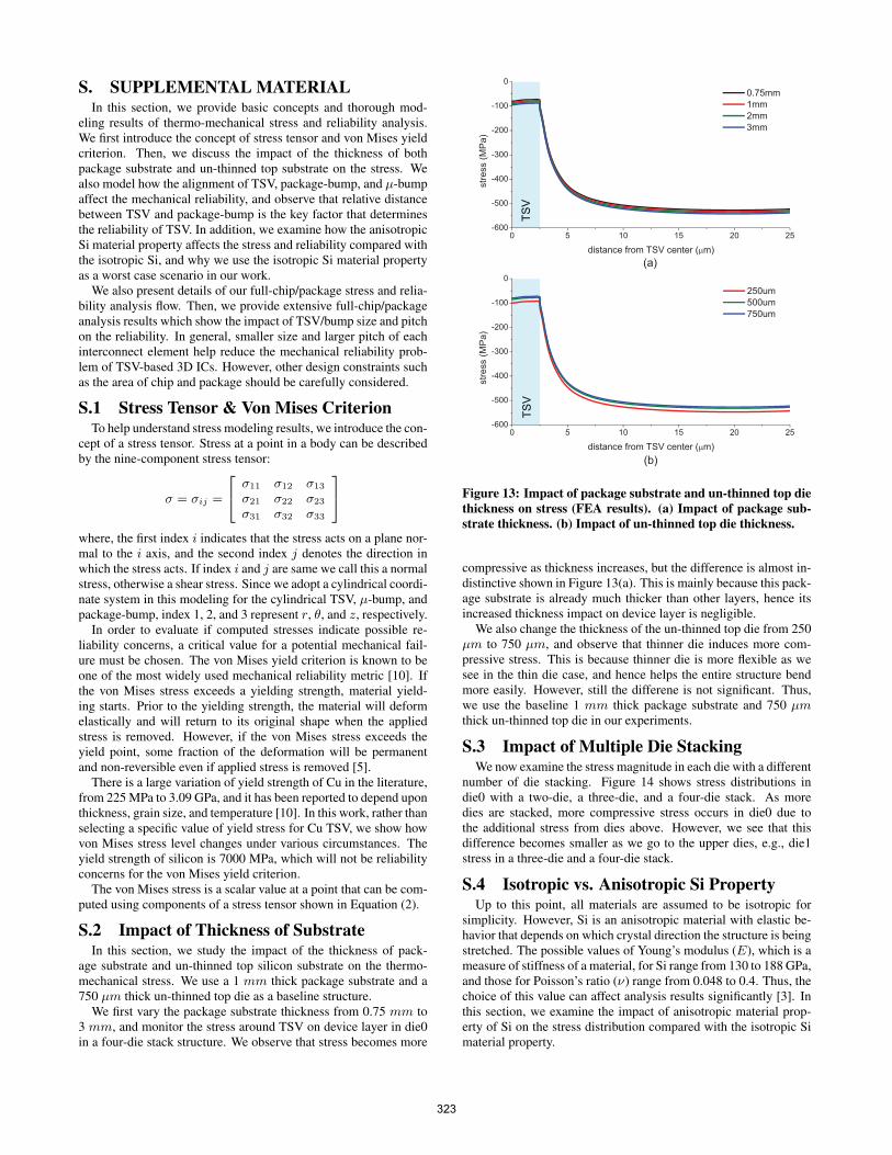
S. SUPPLEMENTAL MATERIALIn this section, we provide basic concepts and thorough mod-
eling results of thermo-mechanical stress and reliability analysis.We first introduce the concept of stress tensor and von Mises yieldcriterion. Then, we discuss the impact of the thickness of bothpackage substrate and un-thinned top substrate on the stress. Wealso model how the alignment of TSV, package-bump, and µ-bumpaffect the mechanical reliability, and observe that relative distancebetween TSV and package-bump is the key factor that determinesthe reliability of TSV. In addition, we examine how the anisotropicSi material property affects the stress and reliability compared withthe isotropic Si, and why we use the isotropic Si material propertyas a worst case scenario in our work.
We also present details of our full-chip/package stress and relia-bility analysis flow. Then, we provide extensive full-chip/packageanalysis results which show the impact of TSV/bump size and pitchon the reliability. In general, smaller size and larger pitch of eachinterconnect element help reduce the mechanical reliability prob-lem of TSV-based 3D ICs. However, other design constraints suchas the area of chip and package should be carefully considered.
S.1 Stress Tensor & Von Mises CriterionTo help understand stress modeling results, we introduce the con-
cept of a stress tensor. Stress at a point in a body can be describedby the nine-component stress tensor:
σ = σij =
σ11 σ12 σ13
σ21 σ22 σ23
σ31 σ32 σ33
where, the first index i indicates that the stress acts on a plane nor-mal to the i axis, and the second index j denotes the direction inwhich the stress acts. If index i and j are same we call this a normalstress, otherwise a shear stress. Since we adopt a cylindrical coordi-nate system in this modeling for the cylindrical TSV, µ-bump, andpackage-bump, index 1, 2, and 3 represent r, θ, and z, respectively.
In order to evaluate if computed stresses indicate possible re-liability concerns, a critical value for a potential mechanical fail-ure must be chosen. The von Mises yield criterion is known to beone of the most widely used mechanical reliability metric [10]. Ifthe von Mises stress exceeds a yielding strength, material yield-ing starts. Prior to the yielding strength, the material will deformelastically and will return to its original shape when the appliedstress is removed. However, if the von Mises stress exceeds theyield point, some fraction of the deformation will be permanentand non-reversible even if applied stress is removed [5].
There is a large variation of yield strength of Cu in the literature,from 225 MPa to 3.09 GPa, and it has been reported to depend uponthickness, grain size, and temperature [10]. In this work, rather thanselecting a specific value of yield stress for Cu TSV, we show howvon Mises stress level changes under various circumstances. Theyield strength of silicon is 7000 MPa, which will not be reliabilityconcerns for the von Mises yield criterion.
The von Mises stress is a scalar value at a point that can be com-puted using components of a stress tensor shown in Equation (2).
S.2 Impact of Thickness of SubstrateIn this section, we study the impact of the thickness of pack-
age substrate and un-thinned top silicon substrate on the thermo-mechanical stress. We use a 1 mm thick package substrate and a750 µm thick un-thinned top die as a baseline structure.
We first vary the package substrate thickness from 0.75 mm to3 mm, and monitor the stress around TSV on device layer in die0in a four-die stack structure. We observe that stress becomes more
(a)
(b)
TSV
TSV
Figure 13: Impact of package substrate and un-thinned top diethickness on stress (FEA results). (a) Impact of package sub-strate thickness. (b) Impact of un-thinned top die thickness.
compressive as thickness increases, but the difference is almost in-distinctive shown in Figure 13(a). This is mainly because this pack-age substrate is already much thicker than other layers, hence itsincreased thickness impact on device layer is negligible.
We also change the thickness of the un-thinned top die from 250µm to 750 µm, and observe that thinner die induces more com-pressive stress. This is because thinner die is more flexible as wesee in the thin die case, and hence helps the entire structure bendmore easily. However, still the differene is not significant. Thus,we use the baseline 1 mm thick package substrate and 750 µmthick un-thinned top die in our experiments.
S.3 Impact of Multiple Die StackingWe now examine the stress magnitude in each die with a different
number of die stacking. Figure 14 shows stress distributions indie0 with a two-die, a three-die, and a four-die stack. As moredies are stacked, more compressive stress occurs in die0 due tothe additional stress from dies above. However, we see that thisdifference becomes smaller as we go to the upper dies, e.g., die1stress in a three-die and a four-die stack.
S.4 Isotropic vs. Anisotropic Si PropertyUp to this point, all materials are assumed to be isotropic for
simplicity. However, Si is an anisotropic material with elastic be-havior that depends on which crystal direction the structure is beingstretched. The possible values of Young’s modulus (E), which is ameasure of stiffness of a material, for Si range from 130 to 188 GPa,and those for Poisson’s ratio (ν) range from 0.048 to 0.4. Thus, thechoice of this value can affect analysis results significantly [3]. Inthis section, we examine the impact of anisotropic material prop-erty of Si on the stress distribution compared with the isotropic Simaterial property.
323

σv =
√(σxx − σyy)2 + (σyy − σzz)2 + (σzz − σxx)2 + 6(σ2
xy + σ2yz + σ2
zx)
2(2)
TSV
Figure 14: σrr stress on die0 with a different number of diestacking.
Elasticity is the relationship between stress (σ) and strain (ϵ).Hooke’s law describes this relationship in terms of stiffness C, i.e.,σ = Cϵ. For isotropic uniaxial cases, stiffness C can be repre-sented by a single value of Young’s modulus E, and the equationtakes the form of σ = Cϵ. In an anisotropic material, a fourthrank stiffness tensor with 34 = 81 terms is required to describe theelasticity. Fortunately, due to the cubic symmetry of Si, the elasticproperties can be expressed in terms of orthotropic material con-stants. An orthotropic material is one which contains at least twoorthogonal planes of symmetry, and Si, with cubic symmetry, canbe described this way. The orthotropic elasticity of Si can be ex-pressed with reference axes of a standard (100) Si wafer, which are[110], [1̄10], and [001],
σxx
σyy
σzz
σyz
σzx
σxy
=
c1 c5 c6 0 0 0c5 c1 c6 0 0 0c6 c6 c2 0 0 00 0 0 c3 0 00 0 0 0 c3 00 0 0 0 0 c4
ϵxxϵyyϵzzϵyzϵzxϵxy
where, orientation specific constants c1, c2, c3, c4, c5, c6 are 194.5,165.7, 79.6, 50.9, 35.7, and 64.1, all in GPa, respectively. Thisstiffness tensor translates to Ex = Ey = 169 GPa, Ez = 130 GPa,νyz = 0.36, νzx = 0.28, and νxy = 0.064 [3].
Figure 15 shows the stress comparison between anisotropic andisotropic Si (Young’s modulus = 188 GPa for all directions) ma-terial properties. We see that the normal stress component be-comes less compressive and the von Mises stress is lower with theanisotropic Si compared with the isotropic Si case. This is largelydue to the fact that we use the maximum Young’s modulus for theisotropic Si case. With higher Young’s modulus Si substrate be-comes stiffer, hence higher stress builds up at the TSV/substrateinterface. In this work, even though anisotropic Si property is morerealistic, we use the isotropic Si property as a worst case scenario.
S.5 Impact of TSV and Bump AlignmentIn this section, we explore the impact of alignment between TSV,
µ-bump, and package-bump on the mechanical reliability of TSVs.We first examine the impact of relative position between TSV/µ-bump and package-bump. We use a two-die stack structure inwhich center locations of TSV, µ-bump, and package-bump arealigned as shown in Figure 16(a). Then we shift both TSV and
(a)
(b)TSV
TSV
Figure 15: Impact of silicon material property on stress (FEAresults). (a) σθθ stress. (b) Von Mises stress.
µ-bump together from the package-bump center with a 25 µm stepand monitor the von Mises stress at the right edge of TSV.
Figure 16(c) shows that the von Mises stress is maximum aroundpackage-bump edge region and then decreases and saturates as dis-tance increases. The difference between minimum and maximumis as high as 11.1 %. As Figure 3 shows, the highest stress gradi-ent occurs around package-bump edge which results in the highestdeformation of the structure near this region. Hence, this higherdeformation causes more severe mechanical reliability problem inTSV.
We also see the decrease in von Mises stress near the package-bump center. This is because the material around this area is thesame (= package-bump material), hence its deformation is rela-tively smaller than the edge which is the interface between twodifferent materials.
We also examine whether relative position between µ-bump andTSV/package-bump affects the mechanical reliability of TSV. Wefix the location of TSV and package-bump whose centers are aligned,then move µ-bump only with a 5 µm step up to 30 µm and monitorthe von Mises stress at TSV edges. We observe the similar trend asbefore. However, the difference between minimum and maximumis only 6.5 MPa (0.8 %), which is negligible. Thus, we identify thatthe relative position between TSV and package-bump is a criticalfactor that affects the mechanical reliability of TSV.
S.6 Full-Chip/Package Analysis AlgorithmIn this section, we discuss details of our full-system-scale thermo-
mechanical stress and reliability analysis flow. First, based on the
324

(a) (b)
(c)
Pkg-bump
Pkg-bump
TSV
μ-bump move
-bump
TSV
μ-bump
300um shi!TSV right edge
Pkg
Figure 16: Impact of relative position between TSV/µ-bumpand package-bump on von Mises stress. (a) Initial position. (b)Final position where TSV/µ-bump are shifted by 300 µm frompackage bump center. (c) Von Mises stress at TSV edge alongthe distance between TSV/µ-bump and package-bump (FEAresults).
observation that the stress field induced by a single TSV, a µ-bump,and a package-bump in isolation is radially symmetrical due to theircylindrical shape, we obtain stress tensors for each interconnectcomponent along an arbitrary radial line on device layer from theircenter location in a cylindrical coordinate system. To evaluate thestress tensor at a point affected by multiple interconnect elements,a conversion of a stress tensor to a Cartesian coordinate system isrequired. This is due to the fact that we extract stress tensors fromthese interconnect components whose center position is the originin the cylindrical coordinate system; hence we cannot perform avector sum of stress tensors from each component which has a dif-ferent center location.
Then, we compute the stress tensor at the point of interest byadding up the stress tensors from TSVs, µ-bumps, and package-bumps that affect this point. We set a stress influence zone of TSV,µ-bump, and package-bump 25 µm, 100 µm, 500 µm from thecenter of each component, which is five times the diameter of eachcomponent, respectively. This is because the magnitude of eachstress tensor component saturates well before this distance, hencethere is a negligible impact from the interconnect element beyondthis stress influence zone.
Let the stress tensor in Cartesian and cylindrical coordinate sys-tem be Sxyz and Srθz , respectively.
Sxyz =
σxx σxy σxz
σyx σyy σyz
σzx σzy σzz
, Srθz =
σrr σrθ σrz
σθr σθθ σθz
σzr σzθ σzz
The transform matrix Q is the form:
Q =
cos θ − sin θ 0sin θ cos θ 00 0 1
where, θ is the angle between the x-axis and a line from the cen-ter of each interconnect element to the simulation grid point. Astress tensor in a cylindrical coordinate system can be converted to
input : TSV list T , pkg-bump list P , µ-bump list M , stresslibrary
output: stress map, von Mises stress mapfor each TSV t, pkg-bump p, and µ-bump m in T , P , and Mdo
(it, ip, im)←− FindStressInfluenceZone(t, p,m)for each point it′, ip′, and im′ in it, ip, and im do
it′.TSV ←− itip′.pkg-bump←− ipim′.µ-bump←− im
endendfor each simulation point r do
if r.TSV ̸= ∅ || r.pkg-bump ̸= ∅ || r.µ-bump ̸= ∅ thenfor each (t, p,m) ∈ (r.TSV ,r.pkg-bump,r.µ-bump)do
(dt, dp, dm)←− distance(t, p,m, r)Scyl(t, p,m)←− GetStressTensor(dt, dp, dm)Scyl(t, p,m)←− Scyl(t, p,m)−BGstressθ(t, p,m)←− GetAngle(line tr, pr,mr, x-axis)Q(t, p,m)←− SetConversionMatrix(θt,θp,θm)SCart(t, p,m)←−Q(t, p,m)Scyl(t, p,m)Q(t, p,m)T
r.SCart ←− r.SCart + SCart(t, p,m)
endendr.SCart ←− r.SCart +BGstressvonMises(r)←− ComputeVonMises(r.Scart)
endAlgorithm 1: Full-Chip/Package Stress and Reliability Analy-sis Flow (LVLS)
a Cartesian coordinate system using conversion matrices: Sxyz =QSrθzQ
T [5].Our full-system-scale thermo-mechanical stress and reliability
analysis flow is shown in Algorithm 1. We first start to find a stressinfluence zone from each TSV, µ-bump, and package-bump. Then,we associate the points in the influence zone with the affecting in-terconnect elements. Next, for each grid point under consideration,we look up the stress tensors from each interconnect componentfound in the association step, and subtract background stress fromthe stress tensor. Then, we use the coordinate conversion matricesto obtain stress tensors in the Cartesian coordinate system. We visitan individual TSV, µ-bump, and package-bump affecting this sim-ulation point and add up their stress contributions. After visiting allthe components effecting this point, we add one background stressback. Once we finish the stress computation at the point, we obtainthe von Mises stress value using Equation (2).
S.7 Impact of Bump SizeIn this section, we study the impact of package-bump and µ-
bump size on the reliability. First, we vary the package-bump di-ameter/height from 100 µm to 300 µm, while fixing the package-bump pitch and the TSV/µ-bump count and pitch as 400 µm, 1600,and 20 µm, respectively. Table 4 shows that the number of TSVsexperiencing higher von Mises stress increases with larger package-bumps due to the larger deformation of a stack and the increasedpackage-bump circumference where highest von Mises stress oc-curs. However, in the 300 µm package-bump case, there are moreTSVs with lower von Mises stress (780 - 870 MPa) than the 200µm package-bump case. As discussed in Section S.5, TSVs lo-
325
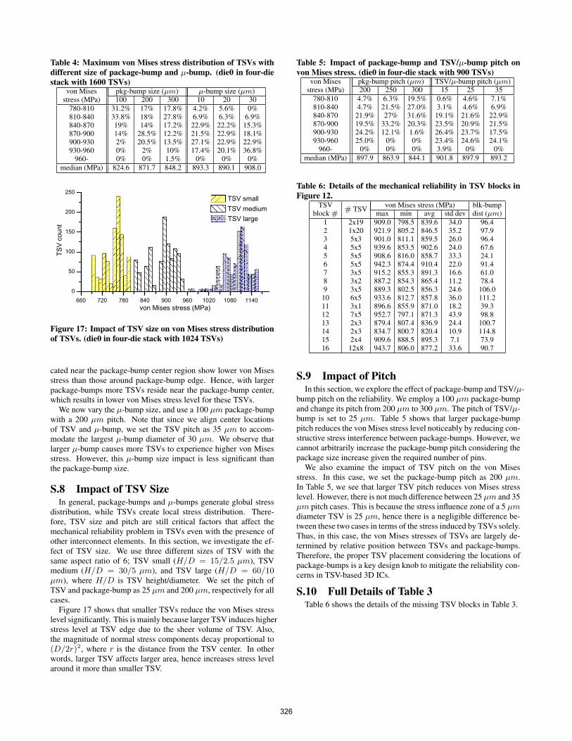
Table 4: Maximum von Mises stress distribution of TSVs withdifferent size of package-bump and µ-bump. (die0 in four-diestack with 1600 TSVs)
von Mises pkg-bump size (µm) µ-bump size (µm)stress (MPa) 100 200 300 10 20 30
780-810 31.2% 17% 17.8% 4.2% 5.6% 0%810-840 33.8% 18% 27.8% 6.9% 6.3% 6.9%840-870 19% 14% 17.2% 22.9% 22.2% 15.3%870-900 14% 28.5% 12.2% 21.5% 22.9% 18.1%900-930 2% 20.5% 13.5% 27.1% 22.9% 22.9%930-960 0% 2% 10% 17.4% 20.1% 36.8%
960- 0% 0% 1.5% 0% 0% 0%median (MPa) 824.6 871.7 848.2 893.3 890.1 908.0
0
50
100
150
200
250
TSV
coun
t
von Mises stress (MPa)
TSV small
660 720 780 840 900 960 1020 1080 1140
TSV medium TSV large
Figure 17: Impact of TSV size on von Mises stress distributionof TSVs. (die0 in four-die stack with 1024 TSVs)
cated near the package-bump center region show lower von Misesstress than those around package-bump edge. Hence, with largerpackage-bumps more TSVs reside near the package-bump center,which results in lower von Mises stress level for these TSVs.
We now vary the µ-bump size, and use a 100 µm package-bumpwith a 200 µm pitch. Note that since we align center locationsof TSV and µ-bump, we set the TSV pitch as 35 µm to accom-modate the largest µ-bump diameter of 30 µm. We observe thatlarger µ-bump causes more TSVs to experience higher von Misesstress. However, this µ-bump size impact is less significant thanthe package-bump size.
S.8 Impact of TSV SizeIn general, package-bumps and µ-bumps generate global stress
distribution, while TSVs create local stress distribution. There-fore, TSV size and pitch are still critical factors that affect themechanical reliability problem in TSVs even with the presence ofother interconnect elements. In this section, we investigate the ef-fect of TSV size. We use three different sizes of TSV with thesame aspect ratio of 6; TSV small (H/D = 15/2.5 µm), TSVmedium (H/D = 30/5 µm), and TSV large (H/D = 60/10µm), where H/D is TSV height/diameter. We set the pitch ofTSV and package-bump as 25 µm and 200 µm, respectively for allcases.
Figure 17 shows that smaller TSVs reduce the von Mises stresslevel significantly. This is mainly because larger TSV induces higherstress level at TSV edge due to the sheer volume of TSV. Also,the magnitude of normal stress components decay proportional to(D/2r)2, where r is the distance from the TSV center. In otherwords, larger TSV affects larger area, hence increases stress levelaround it more than smaller TSV.
Table 5: Impact of package-bump and TSV/µ-bump pitch onvon Mises stress. (die0 in four-die stack with 900 TSVs)
von Mises pkg-bump pitch (µm) TSV/µ-bump pitch (µm)stress (MPa) 200 250 300 15 25 35
780-810 4.7% 6.3% 19.5% 0.6% 4.6% 7.1%810-840 4.7% 21.5% 27.0% 3.1% 4.6% 6.9%840-870 21.9% 27% 31.6% 19.1% 21.6% 22.9%870-900 19.5% 33.2% 20.3% 23.5% 20.9% 21.5%900-930 24.2% 12.1% 1.6% 26.4% 23.7% 17.5%930-960 25.0% 0% 0% 23.4% 24.6% 24.1%
960- 0% 0% 0% 3.9% 0% 0%median (MPa) 897.9 863.9 844.1 901.8 897.9 893.2
Table 6: Details of the mechanical reliability in TSV blocks inFigure 12.
TSV# TSV von Mises stress (MPa) blk-bump
block # max min avg std dev dist (µm)1 2x19 909.0 798.5 839.6 34.0 96.42 1x20 921.9 805.2 846.5 35.2 97.93 5x3 901.0 811.1 859.5 26.0 96.44 5x5 939.6 853.5 902.6 24.0 67.65 5x5 908.6 816.0 858.7 33.3 24.16 5x5 942.3 874.4 910.4 22.0 91.47 3x5 915.2 855.3 891.3 16.6 61.08 3x2 887.2 854.3 865.4 11.2 78.49 3x5 889.3 802.5 856.3 24.6 106.010 6x5 933.6 812.7 857.8 36.0 111.211 3x1 896.6 855.9 871.0 18.2 39.312 7x5 952.7 797.1 871.3 43.9 98.813 2x3 879.4 807.4 836.9 24.4 100.714 2x3 834.7 800.7 820.4 10.9 114.815 2x4 909.6 888.5 895.3 7.1 73.916 12x8 943.7 806.0 877.2 33.6 90.7
S.9 Impact of PitchIn this section, we explore the effect of package-bump and TSV/µ-
bump pitch on the reliability. We employ a 100 µm package-bumpand change its pitch from 200 µm to 300 µm. The pitch of TSV/µ-bump is set to 25 µm. Table 5 shows that larger package-bumppitch reduces the von Mises stress level noticeably by reducing con-structive stress interference between package-bumps. However, wecannot arbitrarily increase the package-bump pitch considering thepackage size increase given the required number of pins.
We also examine the impact of TSV pitch on the von Misesstress. In this case, we set the package-bump pitch as 200 µm.In Table 5, we see that larger TSV pitch reduces von Mises stresslevel. However, there is not much difference between 25 µm and 35µm pitch cases. This is because the stress influence zone of a 5 µmdiameter TSV is 25 µm, hence there is a negligible difference be-tween these two cases in terms of the stress induced by TSVs solely.Thus, in this case, the von Mises stresses of TSVs are largely de-termined by relative position between TSVs and package-bumps.Therefore, the proper TSV placement considering the locations ofpackage-bumps is a key design knob to mitigate the reliability con-cerns in TSV-based 3D ICs.
S.10 Full Details of Table 3Table 6 shows the details of the missing TSV blocks in Table 3.
326