
CHIP MONOLITHIC CERAMIC CAPACITOR FOR … Sheets/Murata PDFs... · Specifications and Test Methods...
29
GRM1555C1HR75BA01_ (0402, C0G, 0.75pF, 50Vdc) _: packaging code Reference Sheet 1.Scope 2.MURATA Part NO. System (Ex.) 3. Type & Dimensions (Unit:mm) 4.Rated value 5.Package Product specifications in this catalog are as of Jan.24,2013,and are subject to change or obsolescence without notice. Please consult the approval sheet before ordering. Please read rating and !Cautions first. CHIP MONOLITHIC CERAMIC CAPACITOR FOR GENERAL g 0.15 to 0.35 0.75 pF Temp. Range (Ref.Temp.) (8) Packaging mark (4) DC Rated Voltage Packaging Unit ±0.1 pF -55 to 125 °C 0±30 ppm/°C 25 to 125 °C (25 °C) (3) Temperature Characteristics (Public STD Code):C0G(EIA) Specifications and Test Methods (Operationg Temp. Range) Temp. coeff or Cap. Change (5) Nominal Capacitance (6) Capacitance Tolerance 50 Vdc 0.3 min. (2) T 0.5±0.05 This product specification is applied to Chip Monolithic Ceramic Capacitor used for General Electronic equipment. (1)-1 L 1.0±0.05 (1)-2 W 0.5±0.05 e J f330mm Reel PAPER W8P2 50000 pcs./Reel D f180mm Reel PAPER W8P2 10000 pcs./Reel W f180mm Reel PAPER W8P1 20000 pcs./Reel (1)L/W Dimensions (2)T Dimensions (3)Temperature Characteristics (4)DC Rated Voltage (5)Nominal Capacitance (6)Capacitance Tolerance (8)Packaging Code (7)Murata’s Control Code T L W e e g GRM 15 5 5C 1H R75 B A01 D GRM1555C1HR75BA01-01 1
Transcript of CHIP MONOLITHIC CERAMIC CAPACITOR FOR … Sheets/Murata PDFs... · Specifications and Test Methods...

GRM1555C1HR75BA01_ (0402, C0G, 0.75pF, 50Vdc)_: packaging code Reference Sheet
1.Scope
2.MURATA Part NO. System(Ex.)
3. Type & Dimensions
(Unit:mm)
4.Rated value
5.Package
Product specifications in this catalog are as of Jan.24,2013,and are subject to change or obsolescence without notice.
Please consult the approval sheet before ordering.
Please read rating and !Cautions first.
CHIP MONOLITHIC CERAMIC CAPACITOR FOR GENERAL
g
0.15 to 0.35
0.75 pF
Temp. Range
(Ref.Temp.)
(8) Packagingmark
(4)
DC Rated
Voltage
Packaging Unit
±0.1 pF -55 to 125 °C0±30 ppm/°C25 to 125 °C
(25 °C)
(3) Temperature Characteristics
(Public STD Code):C0G(EIA)Specifications and Test
Methods
(Operationg
Temp. Range)Temp. coeff
or Cap. Change
(5) Nominal
Capacitance
(6)
Capacitance
Tolerance
50 Vdc
0.3 min.
(2) T
0.5±0.05
This product specification is applied to Chip Monolithic Ceramic Capacitor used for General Electronic equipment.
(1)-1 L
1.0±0.05
(1)-2 W
0.5±0.05
e
Jf330mm Reel
PAPER W8P250000 pcs./Reel
Df180mm Reel
PAPER W8P210000 pcs./Reel
Wf180mm Reel
PAPER W8P120000 pcs./Reel
(1)L/WDimensions
(2)T Dimensions
(3)Temperature Characteristics
(4)DC Rated Voltage
(5)Nominal Capacitance
(6)Capacitance Tolerance
(8)Packaging Code
(7)Murata’s Control Code
T
L
W
e eg
GRM 15 5 5C 1H R75 B A01 D
GRM1555C1HR75BA01-01 1

Temperature
Compensating Type
High Dielectric
Constant Type
1 Operating -55℃ to 125℃ R6:-55℃ to 85℃ Reference Temperature : 25℃
Temperature Range R7:-55℃ to 125℃
C8:-55℃ to 105℃
E4:10℃ to 85℃
F5:-30℃ to 85℃
L8/R9:-55℃ to 150℃
2 Rated Voltage See the previous pages. The rated voltage is defined as the maximum voltage which may be applied
continuously to the capacitor.
When AC voltage is superimposed on DC voltage, VP-P or VO-P, whichever is
larger, should be maintained within the rated voltage range.
3 Appearance No defects or abnormalities. Visual inspection.
4 Dimension Within the specified dimensions. Using calipers. (GRM02 size is based on Microscope)
5 Dielectric Strength No defects or abnormalities. No failure should be observed when 300% of the rated voltage
(ΔC to7U and 1X) or 250% of the rated voltage (R6,R7,C8,E4,F5,L8 and R9)
is applied between the terminations for 1 to 5 seconds, provided the
charge/discharge current is less than 50mA.
6 Insulation More than 10,000MΩ or 500Ω ∙F The insulation resistance should be measured with a DC voltage
Resistance (whichever is smaller) not exceeding the rated voltage at 25℃ and 75%RH max.
and within 2 minutes of charging, provided the charge/discharge
current is less than 50mA.
7 Capacitance Within the specified tolerance. The capacitance/Q/D.F. should be measured at 25℃ at the frequency
and voltage shown in the table.
8 Q/Dissipation 30pF and over:Q≧1000 [R6,R7,C8,L8] (1)Temperature Compensating Type
Factor (D.F.) 30pF and below:Q≧400+20C W.V.:100V :0.025max.(C<0.068mF)
:0.05max.(C≧0.068mF)
C:Nominal Capacitance(pF) W.V.:50V/25V :0.025max.
W.V.:16V/10V :0.035max.
W.V.:6.3V/4V :0.05max.(C<3.3mF)
:0.1max.(C≧3.3mF) (2)High Dielectric Constant Type
[R9]
W.V.:50V: 0.05max.
[E4]
W.V.:25Vmin: 0.025max.
[F5]
W.V.:25Vmin
:0.05max. (C<0.1mF)
:0.09max.(C≧0.1mF)
W.V.:16V/10V:0.125max.
W.V.:6.3V:0.15max.
9 Capacitance Capacitance Within the specified The capacitance change should be measured after 5min. at eachTemperature Change tolerance.(Table A-1) specified temp.stage.
Characteristics (1)Temperature Compensating Type
The temperature coefficient is determind using the capacitance
measured in step 3 as a reference.
When cycling the temperature sequentially from step 1 through
5 (Δ C:+25℃ to +125℃,other temp.coeffs.:+25℃ to +85℃) the capacitance
should be within the specified tolerance for the temperature coefficient
and capacitance change as Table A-1.
The capacitance drift is caluculated by dividing the differences between
the maximum and minimum measured values in the step 1,3 and 5
by the cap.value in step 3.
Temperature Within the specified
Coefficent tolerance.(Table A-1)
Capacitance Within±0.2% or±0.05pF
Drift (Whichever is larger.)
*Not apply to 1X/25V
(2)High Dielectric Constant Type
The ranges of capacitance change compared with the 25℃
value over the temperature ranges shown in the table should be
within the specified ranges.*
Initial measurement for high dielectric constant type
Perform a heat treatment at 150 +0/-10°C for one hour and then set
for 24±2 hours at room temperature.
Perform the initial measure-ment.
10 Adhesive Strength No removal of the terminations or other defect should occur. Solder the capacitor on the test jig (glass epoxy board)shown in
of Termination Fig.3 using a eutectic solder. Then apply 10N* force in parallel
with the test jig for 10±1sec.
The soldering should be done either with an iron or using the
reflow method and should be conducted with care so that the
soldering is uniform and free of defects such as heat shock.
*1N(GRM02),2N(GR□03),5N(GR□15,GRM18)
■SPECIFICATIONS AND TEST METHODS
No ItemSpecification
Test Method
Step Temperature(C)
1 25±2
2 -55±3(for C to 7U/1X)
3 25±2
4 125±3(for Δ C),
85±3(for other TC)
5 25±2
Capacitance Frequency Voltage
C≦10μF 1±0.1kHz 1±0.2Vrms
C>10μF 120±24Hz 0.5±0.1Vrms
E4 1±0.1kHz 0.5±0.05Vrms
Capacitance Frequency Voltage
C≦1000pF 1±0.1MHz 0.5 to 5Vrms
C>1000pF 1±0.1kHz 1±0.2Vrms
Char. Temp. Range
Reference Temp.
Cap. Change
R6 -55C to +85C
25C
Within ±15%
R7 -55C to +125C Within ±15%
C8 -55C to +105C Within ±22%
L8 -55C to +125C Within ±15%
+125C to+150C Within+15/-40%
R9 -55C to+150C Within ±15%
E4 +10C to +85C Within+22/-56%
F5 -30C to +85C Within+22/-82%
Step Temperature(C)
1 25±2
2 -55±3(for R6/R7/C8/L8/R9)
-30±3(for F5) 10±3(for E4)
3 25±2
4 150±3(for L8/R9)
125±3(for R7) 105±3(for C8)
5 25±2
JEMCGS-0015Q 2
Temperature
Compensating Type
High Dielectric
Constant Type11 Vibration Appearance No defects or abnormalities. Solder the capacitor on the test jig (glass epoxy board) in the same
Resistance manner and under the same conditions as (10).
Capacitance Within the specified tolerance. The capacitor should be subjected to a simple harmonic motion
having a total amplitude of 1.5mm, the frequency being varied
Q/D.F. 30pF and over:Q≧1000 [R6,R7,C8,L8] uniformly between the approximate limits of 10 and 55Hz. The
30pF and beloow:Q≧400+20C W.V.:100V :0.025max.(C<0.068mF) frequency range, from 10 to 55Hz and return to 10Hz, should be
:0.05max.(C≧0.068mF) traversed in approximately 1 minute. This motion should be
C:Nominal Capacitance(pF) W.V.:50V/25V :0.025max. applied for a period of 2 hours in each 3 mutually perpendicular
W.V.:16V/10V :0.035max. directions(total of 6 hours).
W.V.:6.3V/4V :0.05max. (C<3.3mF)
:0.1max.(C≧3.3mF)
[R9]
W.V.:50V: 0.05max.
[E4]
W.V.:25V: 0.025max.
[F5]
W.V.:25Vmin
:0.05max. (C<0.1mF)
:0.09max. (C≧0.1mF)
W.V.:16V/10V:0.125max.
W.V.:6.3V:0.15max.
12 Deflection Appearance No defects or abnormalities. Solder the capacitor on the test jig (glass epoxy board) shown in
Fig.1 using an eutectic solder. Then apply a force in the direction
Capacitance Within ±5% or± 0.5pF Within ±10% shown in Fig 2 for 5±1 seconds. The soldering should be done
Change (Whichever is larger) by the reflow method and should be conducted with care so that
the soldering is uniform and free of defects such as heat shock.
13 Solderability 75% of the terminations is to be soldered evenly and continuously. Immerse the capacitor in a solution of ethanol (JIS-K-8101) and
of Termination rosin (JIS-K-5902) (25% rosin in weight propotion) .
Preheat at 80 to 120℃ for 10 to 30 seconds.
After preheating , immerse in an eutectic solder solution for
2±0.5 seconds at 230±5℃ or Sn-3.0Ag-0.5Cu solder solution
for 2±0.5 seconds at 245±5℃.
14 Resistance to The measured and observed characteristics should satisfy Preheat the capacitor at *120 to 150℃ for 1 minute.
Soldering Heat the specifications in the following table. Immerse the capacitor in an eutectic solder solution* or
Sn-3.0Ag-0.5Cu solder solution at 270±5℃ for 10±0.5 seconds.
Appearance No defects or abnormalities. Set at room temperature for 24±2 hours, then measure.
Capacitance Within ±2.5% or± 0.25pF R6,R7,R9,C8,L8:Within ±7.5% *Not apply to GRM02
Change (Whichever is larger) E4,F5 :Within ±20%
Q/D.F. 30pF and over:Q≧1000 [R6,R7,C8,L8] · Initial measurement for high dielectric constant type
30pF and beloow:Q≧400+20C W.V.:100V :0.025max.(C<0.068mF) Perform a heat treatment at 150+0/-10C for one hour and then set
:0.05max.(C≧0.068mF) at room temperature for 24±2 hours.
C:Nominal Capacitance(pF) W.V.:50V/25V :0.025max. Perform the initial measurement.
W.V.:16V/10V :0.035max.
W.V.:6.3V/4V :0.05max. (C<3.3mF)
:0.1max.(C≧3.3mF) *Preheating for GRM32/43/55
[R9]
W.V.:50V: 0.05max.
[E4]
W.V.:25V: 0.025max.
[F5]
W.V.:25Vmin
:0.05max. (C<0.1mF)
:0.09max. (C≧0.1mF)
W.V.:16V/10V:0.125max.
W.V.:6.3V:0.15max.
I.R. More than 10,000MW or 500W·F(Whichever is smaller)
Dielectric No defects.
Strength
15 Temperature Cycle The measured and observed characteristics should satisfy Fix the capacitor to the supporting jig in the same
the specifications in the following table. manner and under the same conditions as (10).
Perform the five cycles according to the four heat
Appearance No defects or abnormalities. treatments shown in the following table.
Set for 24±2 hours at room temperature, then measure.
Capacitance Within ±2.5% or± 0.25pF R6,R7,R9,C8,L8:Within ±7.5%
Change (Whichever is larger) E4,F5 :Within ±20%
Q/D.F. 30pF and over:Q≧1000 [R6,R7,C8,L8]
30pF and beloow:Q≧400+20C W.V.:100V :0.025max.(C<0.068mF)
:0.05max.(C≧0.068mF)
C:Nominal Capacitance(pF) W.V.:50V/25V :0.025max.
W.V.:16V/10V :0.035max.
W.V.:6.3V/4V :0.05max. (C<3.3mF)
:0.1max.(C≧3.3mF) · Initial measurement for high dielectric constant type
[R9] Perform a heat treatment at 150+0/-10C for one hour and then set
W.V.:50V: 0.05max. at room temperature for 24±2 hours.
[E4] Perform the initial measurement.
W.V.:25V: 0.025max.
[F5]
W.V.:25Vmin
:0.05max. (C<0.1mF)
:0.09max. (C≧0.1mF)
W.V.:16V/10V:0.125max.
W.V.:6.3V:0.15max.
I.R. More than 10,000MW or 500W·F(Whichever is smaller)
Dielectric No defects.
Strength
■SPECIFICATIONS AND TEST METHODS
No ItemSpecification
Test Method
Step Temperature Time
1 100C to 120C 1 min.
2 170C to 200C 1 min.
Step Temp.(C) Time (min)
1 Min.
Operating Temp.+0/-3 30±3
2 Room Temp 2 to 3
3 Max.
Operating Temp.+3/-0 30±3
4 Room Temp 2 to 3
JEMCGS-0015Q 3
Temperature
Compensating Type
High Dielectric
Constant Type16 Humidity The measured and observed characteristics should satisfy Set the capacitor at 40±2℃ and in 90 to 95% humiduty
Steady
State
the specifications in the following table. for 500±12 hours.
Appearance No defects or abnormalities. Remove and set for 24±2 hours at room temperature, then
Capacitance Within ±5% or± 0.5pF R6,R7,R9,C8,L8:Within ±12.5% measure.
Change (Whichever is larger) E4,F5 :Within ±30%
Q/D.F. 30pF and over:Q≧350 [R6,R7,R9,C8,L8]
10pF and over W.V.:100V :0.05max.( C<0.068mF)30pF and below:Q≧275+5C/2 :0.075max.(C≧0.068mF)
10pF and below:Q≧200+10C W.V.:50V/25V :0.05max.
W.V.:16V/10V :0.05max.
C:Nominal Capacitance(pF) W.V.:6.3V/4V :0.075max.(C<3.3mF)
:0.125max.(C≧3.3mF)[R9]
W.V.:50V: 0.075max.
[E4]
W.V.:25V: 0.05max.
[F5]
W.V.:25Vmin
:0.075max. (C<0.1mF)
:0.125max. (C≧0.1mF)W.V.:16V/10V:0.15max.
W.V.:6.3V:0.2max.
I.R. More than 1,000MW or 50W·F(Whichever is smaller)
Dielectric No defects.
Strength
17 Humidity Load The measured and observed characteristics should satisfy Apply the rated voltage at 40±2℃ and 90 to 95% humidity for 500
the specifications in the following table. ±12 hours. Remove and set for 24±2 hours at room temprature,
then muasure. The charge/discharge current is less than 50mA.
Appearance No defects or abnormalities.
Capacitance Within ±7.5% or±0.75pF R6,R7,R9,C8,L8:Within ±12.5% · Initial measurement for F5/10Vmax.
Change (Whichever is larger) E4 :Within ±30% Apply the rated DC voltage for 1 hour at 40±2C.F5 :Within ±30%(W.V.>10V) Remove and set for 24±2 hours at room temperature.
F5 :Within+30/-40%(W.V.≦10V) Perform initial measurement.
Q/D.F. 30pF and over:Q≧200 [R6,R7,R9,C8,L8]
30pF and below:Q≧100+10C/3 W.V.:100V :0.05max.( C<0.068mF)
:0.075max.(C≧0.068mF)
C:Nominal Capacitance(pF) W.V.:50V/25V :0.05max.
W.V.:16V/10V :0.05max.
W.V.:6.3V/4V :0.075max.(C<3.3mF)
:0.125max.(C≧3.3mF)
[R9]
W.V.:50V: 0.075max.
[E4]
W.V.:25V: 0.05max.
[F5]
W.V.:25Vmin
:0.075max. (C<0.1mF)
:0.125max. (C≧0.1mF)
W.V.:16V/10V:0.15max.
W.V.:6.3V:0.2max.
I.R. More than 500MΩ or 25Ω·F(Whichever is smaller)
Dielectric No defects.
Strength
18 High Temperature The measured and observed characteristics should satisfy Apply 200% of the rated voltage at the maximum operating
Load the specifications in the following table. temperature ±3℃ for 1000±12 hours.
Set for 24±2 hours at room temperature, then measure.
Appearance No defects or abnormalities. The charge/discharge current is less than 50mA.
Capacitance Within ±3% or ±0.3pF R6,R7,R9,C8,L8:Within ±12.5%
Change (Whichever is larger) E4 :Within ±30% ・Initial measurement for high dielectric constant type.
F5 :Within ±30%(Cap<1.0 mF) Apply 200% of the rated DC voltage at the maximun operating
F5 :Within+30/-40%(Cap≧1.0 mF) temperature ±3C for one hour. Remove and set forQ/D.F. 30pF and over:Q≧350 [R6,R7,R9,C8,L8] 24±2 hours at room temperature.
10pF and over W.V.:100V :0.05max.( C<0.068mF) Perform initial measurement.
30pF and below: Q≧275+5C/2 :0.075max.(C≧0.068mF)
10pF and below:Q≧200+10C W.V.:50V/25V :0.05max.
W.V.:16V/10V :0.05max.
C:Nominal Capacitance (pF) W.V.:6.3V/4V :0.075max.(C<3.3mF)
:0.125max.(C≧3.3mF)
[R9]
W.V.:50V: 0.075max.
[E4]
W.V.:25V: 0.05max.
[F1,F5]
W.V.:25Vmin
:0.075max. (C<0.1mF)
:0.125max. (C≧0.1mF)
W.V.:16V/10V:0.15max.
W.V.:6.3V:0.2max.
I.R. More than 1,000MW or 50W·F(Whichever is smaller)
Dielectric No defects.
Strength
■SPECIFICATIONS AND TEST METHODS
No ItemSpecification
Test Method
Table A-1
Char.
Nominal
Values
(ppm/C) *
Capacitance Change from 25C (%)
-55 -30 -10
Max. Min. Max. Min. Max. Min.
5C 0±30 0.58 -0.24 0.40 -0.17 0.25 -0.11
6C 0±60 0.87 -0.48 0.59 -0.33 0.38 -0.21
6P -150± 60 2.33 0.72 1.61 0.50 1.02 0.32
6R -220± 60 3.02 1.28 2.08 0.88 1.32 0.56
6S -330± 60 4.09 2.16 2.81 1.49 1.79 0.95
6T -470± 60 5.46 3.28 3.75 2.26 2.39 1.44
7U -750±120 8.78 5.04 6.04 3.47 3.84 2.21
1X +350~-1000 - - - - - -
* Nominal values denote the temperature coefficient within a range of 25C to 125C(for C)/ 85C(for other TC).
JEMCGS-0015Q 4

Adhesive Strength of Termination,Vibration Resistance,Temperature Cycle,
Test method : Deflection Humidity Steady State,Humidity Load,High Temperature Load
・Test substrate ・Test substrate
Material : Copper-clad laminated sheets for PCBs Material : Copper-clad laminated sheets for PCBs
(Glass fabric base, epoxy resin) (Glass fabric base, epoxy resin)
Thickness : 1.6mm(GRM02/03/GR□15: t:0.8mm) Thickness : 1.6mm(GRM02/03/GR□15: t:0.8mm)
Copper foil thickness : 0.035mm Copper foil thickness : 0.035mm
Gray colored part of Fig.1: Solder resist
(Coat with heat resistant resin for solder)
Fig.1 (in:mm) Fig.3 (in:mm)
Fig.2 (in:mm)
■SPECIFICATIONS AND TEST METHODS
Type Dimension (mm)
a b c
GRM02 0.2 0.56 0.23
GR□03 0.3 0.9 0.3
GR□15 0.4 1.5 0.5
GRM18 1.0 3.0 1.2
GRM21 1.2 4.0 1.65
GRM31 2.2 5.0 2.0
GRM32 2.2 5.0 2.9
GRM43 3.5 7.0 3.7
GRM55 4.5 8.0 5.6
*2
4.0±0.1
8.0±
0.3
3.5±
0.05
0.05以下
*1φ1.5+0.1-0
A
t
*1,2:2.0±0.05
1.75
±0.
1
B
100 4
0
a
c
b Land f4.5
c
*2
4.0±0.1
8.0±
0.3
3.5±
0.05
0.05以下
*1φ1.5+0.1-0
A
t
*1,2:2.0±0.05
1.75
±0.
1
B
a
c
b ランド f4.5
c
Glass epoxy board
Solder resist
Baked electrode or copper foil
b
45 45
R230
20 50
Flexure:≦1
Capacitance meter
Pressurization
speed
1.0mm/s
Support
Capacitor Pressurize
45 45
Type Dimension (mm)
a b c
GRM02 0.2 0.56 0.23
GR□03 0.3 0.9 0.3
GR□15 0.4 1.5 0.5
GRM18 1.0 3.0 1.2
GRM21 1.2 4.0 1.65
GRM31 2.2 5.0 2.0
GRM32 2.2 5.0 2.9
GRM43 3.5 7.0 3.7
GRM55 4.5 8.0 5.6
JEMCGS-0015Q 5

1.Tape Carrier Packaging(Packaging Code:D/E/W/F/L/J/K) 1.1 Minimum Quantity(pcs./reel)
φ180mm reel φ330mm reel
Plastic Tape Paper Tape Plastic Tape
Code:D/E Code:W Code:L Code:J/ F Code:K
GR□02 40000 (W4P1)
GR□03 15000(W8P2) 30000(W8P1) 50000(W8P2)
2 20000 50000
3/X 10000 50000
5 (Dimensions Tolerance:±0.05) 10000(W8P2) 20000(W8P1) 50000(W8P2)
5 (Dimensions Tolerance:±0.1min.) 10000 40000
GR□18 4000 10000
5/6/9 4000 3000 10000
A/B 3000 10000
6/9 4000 10000
M/X 3000 10000
C 2000 6000
5/6/9 4000 10000
A/M 3000 10000
N 2000 8000
C 2000 6000
R/D/E 1000 4000
M 1000 5000
N/C/R/D 1000 4000
E 500 2000
S 500 1500
M 1000 5000
N/C/R/D 1000 4000
E 500
F/X 300 1500
1.2 Dimensions of Tape(1)GR□02 (W4P1 CODE:L) (in:mm)
Code GR□02A *3 0.23B *3 0.43 *3 Nominal value
t 0.5 max.
Package
GRM/F Type
Type
GR□21
GR□31
GR□32
GR□43
Paper Tape
GR□55
GR□15
t
2.0±0.04
*2*1φ0.8±0.04 0.
9±0.05
4.0±
0.05
1.8±
0.02
*1,2:1.0±0.02
0.05以下
A
B
0.15~0.4
*1,2:1.0±0.02 2.0±0.04
*1
0.9±
0.05
4.0±
0.05
1.8±
0.02
A
B
t
*2
0.05 max.
φ0.8±0.04 0.15~0.4
JEMCGP-01796 6
(in:mm)
(2)GR□03/15(W8P2 CODE:D/E/J/F)
(3)GRM03/15(W8P1 CODE:W) (in:mm)
Package
GRM/F Type
*1,2:2.0±0.05
*2
4.0±0.1
8.0±
0.3
3.5±
0.05
0.05以下
*1φ1.5+0.1-0
A
t
*1,2:2.0±0.05
1.75
±0.
1
B
4.0±0.1
*1 φ1.5
+0.1 -0 1.
75±0.1
8.0±
0.3
3.5±
0.05
A
B
t
*2
0.05 max.
Code
GR□03
(Dimensions
Tolerance
±0.03)
GR□03
(Dimensions
Tolerance
±0.05)
GR□15
(Dimensions
Tolerance
±0.05)
GR□15
(Dimensions
Tolerance
±0.1)
GR□15
(Dimensions
Tolerance
±0.15)
GR□15
(Dimensions
Tolerance
±0.2)
A*3 0.37 0.39 0.65 0.70 0.72 0.75
B*3 0.67 0.69 1.15 1.20 1.25 1.35
t 0.5max. 0.5 max. 0.8 max. 0.8 max. 0.8 max. 0.8 max. *3 Nominal value
1.0±0.05
4.0±0.1
φ1.5 +0.1 -0 1.
75±
0.1
8.0±
0.3
3.5±
0.05
A
B
t
1.0±0.05
Code GRM03 GRM15
A* 0.37 0.65
B* 0.67 1.15
t 0.5max. 0.8max. *Nominal value
JEMCGP-01796 7

(4)GR□18/21/31/32 T:0.85 rank max. (in:mm)
(5)GR□21/31/32 T:1.0 rank min. (in:mm)
Package
GRM/F Type
4.0±0.1 4.0±0.1
2.0±0.1 φ1.5
+0.1 -0
1.75
±0.
1
8.0±
0.3
3.5±
0.05
0.8 max.(T=0.5mm)
1.15 max.(T≦0.85mm)
A B
Code
GR□18
(Dimensions Tolerance
±0.15within)
GR□18
(Dimensions Tolerance
±0.2)
GR□18
(Dimensions Tolerance
L:±0.2/ W,T:±0.1)
GR□21 GR□31 GR□32
A 1.05±0.1 1.10±0.1 1.05±0.1 1.55±0.15 2.0±0.2 2.8±0.2
B 1.85±0.1 2.00±0.1 2.00±0.1 2.3±0.15 3.6±0.2 3.6±0.2
8.0±
0.3
4.0±0.1
3.5±
0.05
1.75±
0.1
A
B
*
2.0±0.1
φ1.5 +0.1 -0
*
1.7 max.(T≦1.25mm)
2.5 max. (T:1.35/1.6mm)
3.0 max. (T:1.8/2.0mm)
3.7 max. (T≧2.5mm)
4.0±0.1 0.25±0.1(T≦2.0mm)
0.3±0.1(T:2.5mm)
Code
GR□21
(Dimensions Tolerance:
±0.1)
GR□21
(Dimensions Tolerance :
±0.15 /±0.2)
GR□31
(Dimensions Tolerance:
±0.2 within)
GR□31
(Dimensions Tolerance:
±0.3)
GR□32
A 1.45±0.2 1.5±0.2 1.9±0.2 2.1±0.2 2.8±0.2
B 2.25±0.2 2.3±0.2 3.5±0.2 3.6±0.2 3.5±0.2
JEMCGP-01796 8

(6)GR□43/55 (in:mm)
Code GR□43 GR□55A *2 3.6 5.2B *2 4.9 6.1 *2 Nominal value
Package
GRM/F Type
φ1.5 +0.1 -0
4.0±0.1 8.0±0.1
φ1.5 +0.2 -0
12.0±0.3
5.5±
0.1
1.75±
0.1
A
*
2.0±0.1
*1
2.5 max.(T≦1.8mm)
3.7 max.(T=2.0/2.5mm)
4.7 max.(T≧2.8mm)
4.0±0.1
B
*1
*:2.0±0.1
0.3±0.1
JEMCGP-01796 9

Package
GRM/F Type
図 1 チップ詰め状態
( 単位: mm)
φ21±0.8
w1
W
Top Tape : Thickness 0.06
Feeding Hole :As specified in 1.2.
Hole for Chip : As specified in 1.2.
Base Tape : As specified in 1.2.
Bottom Tape :Thickness 0.05 (Only a bottom tape existence )
W w1
GR□02 8.0 max. 5±1.5
GR□32 max. 16.5 max. 10±1.5
GR□43/55 20.5 max. 14±1.5
φ180+
0/-
3.0
φ330±2.0
φ50 m
in.
φ13±0.5
2.0±0.5
Chip
(in:mm) Fig.1 Package Chips
Fig.2 Dimensions of Reel
Fig.3 Taping Diagram
JEMCGP-01796 10
1.3 Tapes for capacitors are wound clockwise shown in Fig.3. (The sprocket holes are to the right as the tape is pulled toward the user.)
1.4 Part of the leader and part of the vacant section are attached as follows.
(in:mm)
1.5 Accumulate pitch : 10 of sprocket holes pitch = 40±0.3mm
1.6 Chip in the tape is enclosed by top tape and bottom tape as shown in Fig.1.
1.7 The top tape and base tape are not attached at the end of the tape for a minimum of 5 pitches.
1.8 There are no jointing for top tape and bottom tape.
1.9 There are no fuzz in the cavity.
1.10 Break down force of top tape : 5N min. Break down force of bottom tape : 5N min. (Only a bottom tape existence )
1.11 Reel is made by resin and appeaser and dimension is shown in Fig 2. There are possibly to change the material and dimension due to some impairment.
1.12 Peeling off force : 0.1N to 0.6N* in the direction as shown below.
* GR□02/03:0.05N~0.5N
1.13 Label that show the customer parts number, our parts number, our company name, inspection number and quantity, will be put in outside of reel.
Package
GRM/F Type
図 1 チップ詰め状態
( 単位: mm)
Tail vacant Section Chip-mounting Unit Leader vacant Section
Leader Unit
(Top Tape only)
Direction of Feed
160 min. 190 min. 210 min.
図 1 チップ詰め状態
( 単位: mm)
165~180° Top tape
JEMCGP-01796 11
Caution
■ Limitation of use Please contact our sales representatives or product engineers before using our products for the applications
listed below which require of our products for other applications than specified in this product.
①Aircraft equipment ②Aerospace equipment ③Undersea equipment ④Power plant control equipment
⑤Medical equipment ⑥Transportation equipment(vehicles,trains,ships,etc.) ⑦Traffic signal equipment
⑧Disaster prevention / crime prevention equipment ⑨Data-processing equipment
⑩Application of similar complexity and/or requirements to the applications listed in the above
■ Storage and Operation condition
1. The performance of chip monolithic ceramic capacitors may be affected by the storage conditions.
1-1. Store capacitors in the following conditions: Temperature of +5℃ to +40℃ and a Relative Humidity
of 20% to 70%.
(1) Sunlight, dust, rapid temperature changes, corrosive gas atmosphere or high temperature and humidity
conditions during storage may affect the solderability and the packaging performance
Please use product within six months of receipt.
(2) Please confirm solderability before using after six months.
Store the capacitors without opening the original bag.
Even if the storage period is short, do not exceed the specified atmospheric conditions.
1-2. Corrosive gas can react with the termination (external) electrodes or lead wires of capacitors, and result
in poor solderability. Do not store the capacitors in an atmosphere consisting of corrosive gas (e.g.,
hydrogen sulfide, sulfur dioxide, chlorine, ammonia gas etc.).
1-3. Due to moisture condensation caused by rapid humidity changes, or the photochemical change caused
by direct sunlight on the terminal electrodes and/or the resin/epoxy coatings, the solderability and
electrical performance may deteriorate. Do not store capacitors under direct sunlight or in high huimidity
conditions
!
JEMCGC-2701V 12
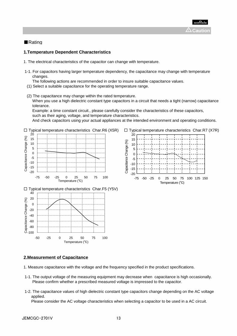
■Rating
1.Temperature Dependent Characteristics
1. The electrical characteristics of the capacitor can change with temperature.
1-1. For capacitors having larger temperature dependency, the capacitance may change with temperature
changes.
The following actions are recommended in order to insure suitable capacitance values.
(1) Select a suitable capacitance for the operating temperature range.
(2) The capacitance may change within the rated temperature.
When you use a high dielectric constant type capacitors in a circuit that needs a tight (narrow) capacitance
tolerance.
Example: a time constant circuit., please carefully consider the characteristics of these capacitors,
such as their aging, voltage, and temperature characteristics.
And check capacitors using your actual appliances at the intended environment and operating conditions.
□ Typical temperature characteristics Char.R6 (X5R) □ Typical temperature characteristics Char.R7 (X7R)
□ Typical temperature characteristics Char.F5 (Y5V)
2.Measurement of Capacitance
1. Measure capacitance with the voltage and the frequency specified in the product specifications.
1-1. The output voltage of the measuring equipment may decrease when capacitance is high occasionally.
Please confirm whether a prescribed measured voltage is impressed to the capacitor.
1-2. The capacitance values of high dielectric constant type capacitors change depending on the AC voltage
applied.
Please consider the AC voltage characteristics when selecting a capacitor to be used in a AC circuit.
Caution
-20
-15
-10
-5
0
5
10
15
20
-75 -50 -25 0 25 50 75 100
Capacitance C
hange (
%)
Temperature (℃)
-100
-80
-60
-40
-20
0
20
40
-50 -25 0 25 50 75 100
Capacitance C
hange (
%)
Temperature (℃)
!
20
15
10
5
0
-5
-10
-15
-20
-75
Capaci
tance
Change (%
)
-50 -25 0 25 50 75 100 125 150
Temperature (℃)
JEMCGC-2701V 13
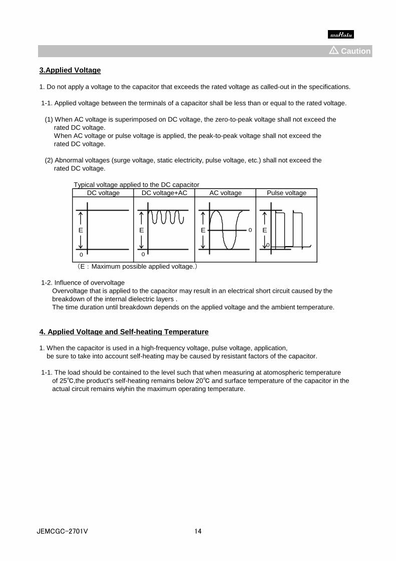
3.Applied Voltage
1. Do not apply a voltage to the capacitor that exceeds the rated voltage as called-out in the specifications.
1-1. Applied voltage between the terminals of a capacitor shall be less than or equal to the rated voltage.
(1) When AC voltage is superimposed on DC voltage, the zero-to-peak voltage shall not exceed the
rated DC voltage.
When AC voltage or pulse voltage is applied, the peak-to-peak voltage shall not exceed the
rated DC voltage.
(2) Abnormal voltages (surge voltage, static electricity, pulse voltage, etc.) shall not exceed the
rated DC voltage.
Typical voltage applied to the DC capacitor
DC voltage DC voltage+AC AC voltage Pulse voltage
(E:Maximum possible applied voltage.)
1-2. Influence of overvoltage
Overvoltage that is applied to the capacitor may result in an electrical short circuit caused by the
breakdown of the internal dielectric layers .
The time duration until breakdown depends on the applied voltage and the ambient temperature.
4. Applied Voltage and Self-heating Temperature
1. When the capacitor is used in a high-frequency voltage, pulse voltage, application,
be sure to take into account self-heating may be caused by resistant factors of the capacitor.
1-1. The load should be contained to the level such that when measuring at atomospheric temperature
of 25℃,the product's self-heating remains below 20℃ and surface temperature of the capacitor in the
actual circuit remains wiyhin the maximum operating temperature.
Caution!
E E E E
0 0
0
0
JEMCGC-2701V 14
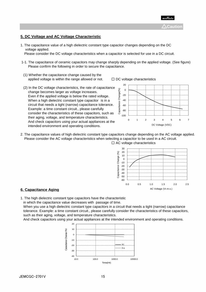
5. DC Voltage and AC Voltage Characteristic
1. The capacitance value of a high dielectric constant type capacitor changes depending on the DC
voltage applied.
Please consider the DC voltage characteristics when a capacitor is selected for use in a DC circuit.
1-1. The capacitance of ceramic capacitors may change sharply depending on the applied voltage. (See figure)
Please confirm the following in order to secure the capacitance.
(1) Whether the capacitance change caused by the
applied voltage is within the range allowed or not. □ DC voltage characteristics
(2) In the DC voltage characteristics, the rate of capacitance
change becomes larger as voltage increases.
Even if the applied voltage is below the rated voltage.
When a high dielectric constant type capacitor is in a
circuit that needs a tight (narrow) capacitance tolerance.
Example: a time constant circuit., please carefully
consider the characteristics of these capacitors, such as
their aging, voltage, and temperature characteristics.
And check capacitors using your actual appliances at the
intended environment and operating conditions.
2. The capacitance values of high dielectric constant type capacitors change depending on the AC voltage applied.
Please consider the AC voltage characteristics when selecting a capacitor to be used in a AC circuit.
□ AC voltage characteristics
6. Capacitance Aging
1. The high dielectric constant type capacitors have the characteristic
in which the capacitance value decreases with passage of time.
When you use a high dielectric constant type capacitors in a circuit that needs a tight (narrow) capacitance
tolerance. Example: a time constant circuit., please carefully consider the characteristics of these capacitors,
such as their aging, voltage, and temperature characteristics.
And check capacitors using your actual appliances at the intended environment and operating conditions.
Caution
-60
-50
-40
-30
-20
-10
0
10
20
30
0.0 0.5 1.0 1.5 2.0 2.5
Capacitance C
hange (
%)
AC Voltage (Vr.m.s.)
-100
-80
-60
-40
-20
0
20
0 1 2 3 4 5 6 7C
apacitance C
hange(%
)
DC Voltage (VDC)
!
20
10
0
-10
-20
-30
-40
10.0 100.0 1000.0 10000.0
Time(Hr)
Cap
acita
nce
Cha
nge
(%)
5C
RΔ
JEMCGC-2701V 15
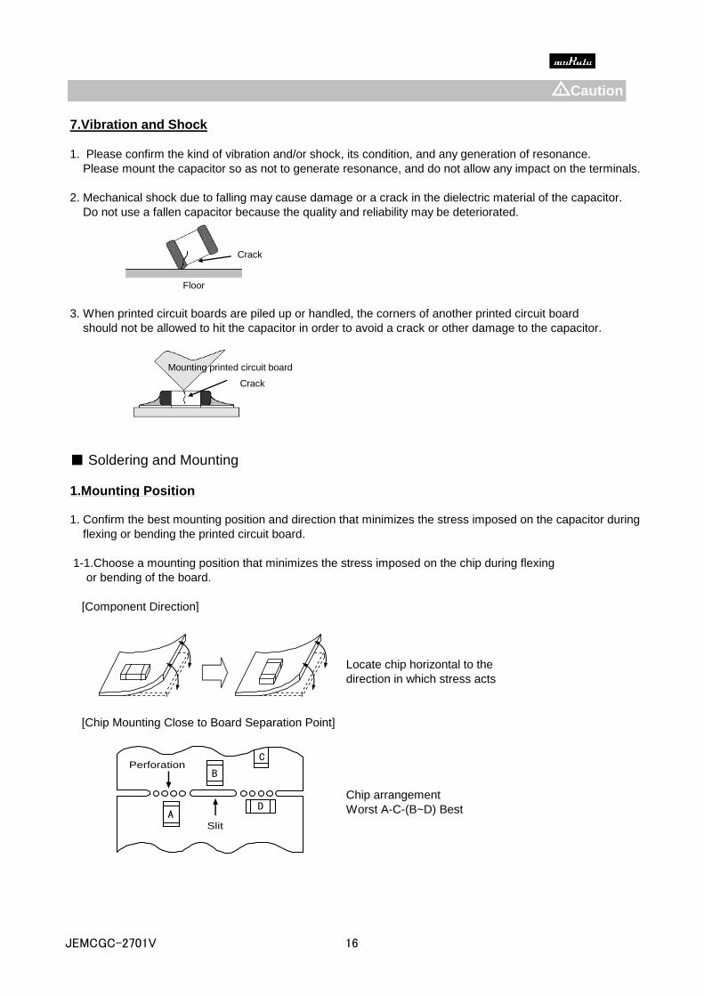
7.Vibration and Shock
1. Please confirm the kind of vibration and/or shock, its condition, and any generation of resonance.
Please mount the capacitor so as not to generate resonance, and do not allow any impact on the terminals.
2. Mechanical shock due to falling may cause damage or a crack in the dielectric material of the capacitor.
Do not use a fallen capacitor because the quality and reliability may be deteriorated.
3. When printed circuit boards are piled up or handled, the corners of another printed circuit board
should not be allowed to hit the capacitor in order to avoid a crack or other damage to the capacitor.
■ Soldering and Mounting
1.Mounting Position
1. Confirm the best mounting position and direction that minimizes the stress imposed on the capacitor during
flexing or bending the printed circuit board.
1-1.Choose a mounting position that minimizes the stress imposed on the chip during flexing
or bending of the board.
[Component Direction]
Locate chip horizontal to the
direction in which stress acts
[Chip Mounting Close to Board Separation Point]
Chip arrangement
Worst A-C-(B~D) Best
Caution
Floor
Crack
Mounting printed circuit board
Crack
!
①
② ③ 1C 1B
1A
Perforation
Slit
A
B
C
D
①
1A
JEMCGC-2701V 16

2.Information before mounting
1. Do Not re-use capacitors that were removed from the equipment.
2. Confirm capacitance characteristics under actual applied voltage.
3. Confirm the mechanical stress under actual process and equipment use.
4. Confirm the rated capacitance, rated voltage and other electrical characteristics before assembly.
5. Prior to use, confirm the Solderability for the capacitors that were in long-term storage.
6. Prior to measuring capacitance, carry out a heat treatment for capacitors that were in long-term storage.
7.The use of Sn-Zn based solder will deteriorate the reliability of the MLCC.
Please contact our sales representative or product engineers on the use of Sn-Zn based solder in advance.
3.Maintenance of the Mounting (pick and place) Machine
1. Make sure that the following excessive forces are not applied to the capacitors.
1-1. In mounting the capacitors on the printed circuit board, any bending force against them shall be kept
to a minimum to prevent them from any bending damage or cracking. Please take into account the
following precautions and recommendations for use in your process.
(1) Adjust the lowest position of the pickup nozzle so as not to bend the printed circuit board.
(2) Adjust the nozzle pressure within a static load of 1N to 3N during mounting.
[Incorrect]
[Correct]
2.Dirt particles and dust accumulated between the suction nozzle and the cylinder inner wall prevent
the nozzle from moving smoothly. This imposes greater force upon the chip during mounting,
causing cracked chips. Also the locating claw, when worn out, imposes uneven forces on the chip
when positioning, causing cracked chips. The suction nozzle and the locating claw must be maintained,
checked and replaced periodically.
Caution!
Board Guide
Board
Suction Nozzle
Deflection
Support Pin
JEMCGC-2701V 17
4-1.Reflow Soldering
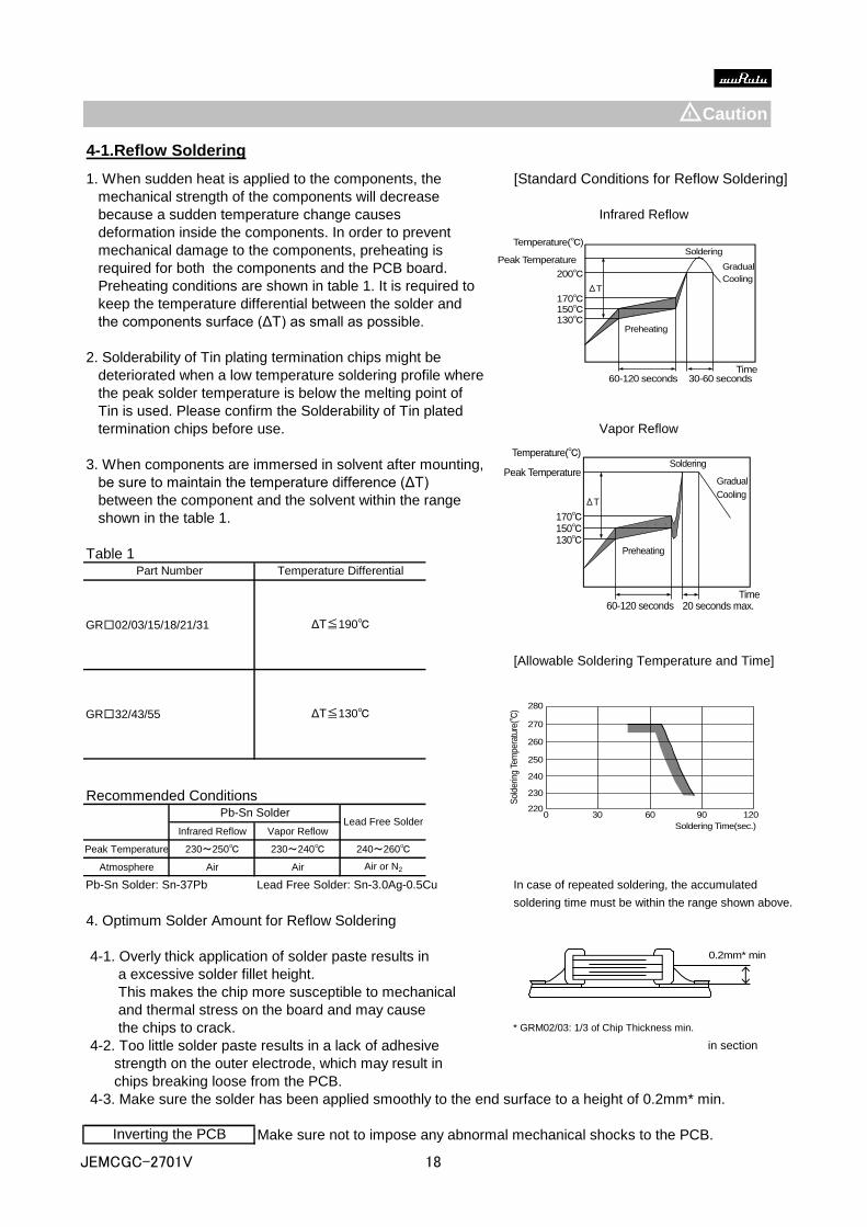
1. When sudden heat is applied to the components, the [Standard Conditions for Reflow Soldering]
mechanical strength of the components will decrease
because a sudden temperature change causes Infrared Reflow
deformation inside the components. In order to prevent
mechanical damage to the components, preheating is
required for both the components and the PCB board.
Preheating conditions are shown in table 1. It is required to
keep the temperature differential between the solder and
the components surface (ΔT) as small as possible.
2. Solderability of Tin plating termination chips might be
deteriorated when a low temperature soldering profile where
the peak solder temperature is below the melting point of
Tin is used. Please confirm the Solderability of Tin plated
termination chips before use. Vapor Reflow
3. When components are immersed in solvent after mounting,
be sure to maintain the temperature difference (ΔT)
between the component and the solvent within the range
shown in the table 1.
Table 1
GR□02/03/15/18/21/31
[Allowable Soldering Temperature and Time]
GR□32/43/55
Recommended Conditions
Infrared Reflow Vapor Reflow
Peak Temperature 230~250℃ 230~240℃ 240~260℃
Atmosphere Air Air Air or N2
Pb-Sn Solder: Sn-37Pb Lead Free Solder: Sn-3.0Ag-0.5Cu In case of repeated soldering, the accumulated
soldering time must be within the range shown above.
4. Optimum Solder Amount for Reflow Soldering
4-1. Overly thick application of solder paste results in
a excessive solder fillet height.
This makes the chip more susceptible to mechanical
and thermal stress on the board and may cause
the chips to crack. * GRM02/03: 1/3 of Chip Thickness min.
4-2. Too little solder paste results in a lack of adhesive in section
strength on the outer electrode, which may result in
chips breaking loose from the PCB.
4-3. Make sure the solder has been applied smoothly to the end surface to a height of 0.2mm* min.
Make sure not to impose any abnormal mechanical shocks to the PCB.Inverting the PCB
Caution
Part Number Temperature Differential
ΔT≦190℃
ΔT≦130℃
Pb-Sn SolderLead Free Solder
!
Temperature(℃)
Peak Temperature
170℃ 150℃ 130℃
200℃
Soldering
Gradual
Cooling
Preheating
ΔT
60-120 seconds 30-60 seconds Time
Sold
erin
g Te
mper
atur
e(℃
)
Soldering Time(sec.)
280
270
260
250
240
230
220 0 30 60 120 90
Temperature(℃)
Peak Temperature
170℃ 150℃ 130℃
ΔT
Soldering
Gradual
Cooling
Preheating
Time 60-120 seconds 20 seconds max.
0.2mm* min
JEMCGC-2701V 18
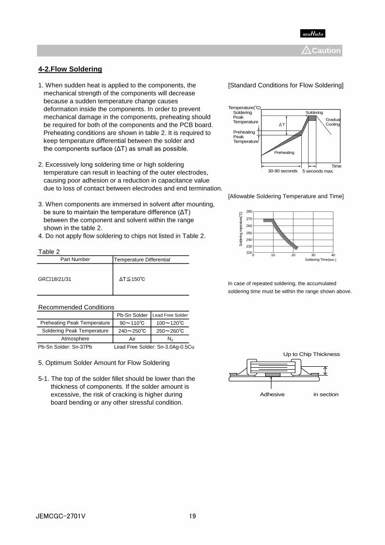
4-2.Flow Soldering
1. When sudden heat is applied to the components, the [Standard Conditions for Flow Soldering]
mechanical strength of the components will decrease
because a sudden temperature change causes
deformation inside the components. In order to prevent
mechanical damage in the components, preheating should
be required for both of the components and the PCB board.
Preheating conditions are shown in table 2. It is required to
keep temperature differential between the solder and
the components surface (ΔT) as small as possible.
2. Excessively long soldering time or high soldering
temperature can result in leaching of the outer electrodes,
causing poor adhesion or a reduction in capacitance value
due to loss of contact between electrodes and end termination.
[Allowable Soldering Temperature and Time]
3. When components are immersed in solvent after mounting,
be sure to maintain the temperature difference (ΔT)
between the component and solvent within the range
shown in the table 2.
4. Do not apply flow soldering to chips not listed in Table 2.
Table 2Temperature Differential
In case of repeated soldering, the accumulated
soldering time must be within the range shown above.
Recommended ConditionsPb-Sn Solder Lead Free Solder
90~110℃ 100~120℃
240~250℃ 250~260℃
Air N2
Pb-Sn Solder: Sn-37Pb Lead Free Solder: Sn-3.0Ag-0.5Cu
5. Optimum Solder Amount for Flow Soldering
5-1. The top of the solder fillet should be lower than the
thickness of components. If the solder amount is
excessive, the risk of cracking is higher during
board bending or any other stressful condition.
Preheating Peak Temperature
Soldering Peak Temperature
Atmosphere
Caution
Part Number
ΔT≦150℃GR□18/21/31
!
Up to Chip Thickness
Adhesive
in section
Sold
erin
g m
pera
ture
(℃)
Soldering Time(sec.)
280
270
260
250
240
230
220 0 10 20 40 30
Temperature(℃) Soldering
Peak Temperature
Preheating Peak Temperature
30-90 seconds
Preheating
5 seconds max. Time
Gradual Cooling
Soldering
ΔT
JEMCGC-2701V 19

4-3.Correction with a Soldering Iron
1. When sudden heat is applied to the components when using a soldering iron, the mechanical strength of
the components will decrease because the extreme temperature change can cause deformations inside the
components. In order to prevent mechanical damage to the components, preheating is required for both
the components and the PCB board. Preheating conditions, (The "Temperature of the Soldering Iron tip",
"Preheating Temperature", "Temperature Differential" between the iron tip and the components and the
PCB), should be within the conditions of table 3. It is required to keep the temperature differential
between the soldering Iron and the component surfaces (ΔT) as small as possible.
2. After soldering, do not allow the component/PCB to rapidly cool down.
3. The operating time for the re-working should be as short as possible. When re-working time is
too long, it may cause solder leaching, and that will cause a reduction in the adhesive
strength of the terminations.
Table 3
*Applicable for both Pb-Sn and Lead Free Solder.Pb-Sn Solder: Sn-37Pb
Lead Free Solder: Sn-3.0Ag-0.5Cu
4. Optimum Solder amount when re-working with a Soldering lron
4-1. In case of sizes smaller than 0603, (GR□03/15/18),
the top of the solder fillet should be lower than 2/3's
of the thickness of the component or 0.5mm whichever
is smaller. In case of 0805 and larger sizes, (GR□21/
31/32/43/55), the top of the solder fillet should be lower in section
than 2/3's of the thickness of the component. If the
solder amount is excessive, the risk of cracking is higher
during board bending or under any other stressful condition.
4-2. A Soldering iron with a tip of ø3mm or smaller should be used. It is also necessary to keep
the soldering iron from touching the components during the re-work.
4-3. Solder wire with ø0.5mm or smaller is required for soldering.
4-4.Leaded Component Insertion
1. If the PCB is flexed when leaded components (such as transformers and ICs) are being mounted,
chips may crack and solder joints may break.
Before mounting leaded components, support the PCB using backup pins or special jigs to prevent warping.
Caution
350℃ max. 150℃ min. ΔT≦190℃ Air
Part NumberTemperature
of Soldering
Iron tip
ΔT≦130℃ Air
Preheating
Temperature
GR□03/15/18/21/31
Temperature
Differential
(ΔT)
Atmosphere
GR□32/43/55 280℃ max. 150℃ min.
!
Solder Amount
JEMCGC-2701V 20

5.Washing
Excessive ultrasonic oscillation during cleaning can cause the PCBs to resonate,
resulting in cracked chips or broken solder joints. Take note not to vibrate PCBs.
6.Electrical Test on Printed Circuit Board
1. Confirm position of the support pin or specific jig, when inspecting the electrical performance of a
capacitor after mounting on the printed circuit board.
1-1. Avoid bending printed circuit board by the pressure of a test pin, etc.
The thrusting force of the test probe can flex the PCB, resulting in cracked chips or open solder joints.
Provide support pins on the back side of the PCB to prevent warping or flexing.
1-2. Avoid vibration of the board by shock when a test pin contacts a printed circuit board.
□ Not recommended □ Recommended
Caution!
Test-pin
Peeling
Test-pin
Support pin
JEMCGC-2701V 21
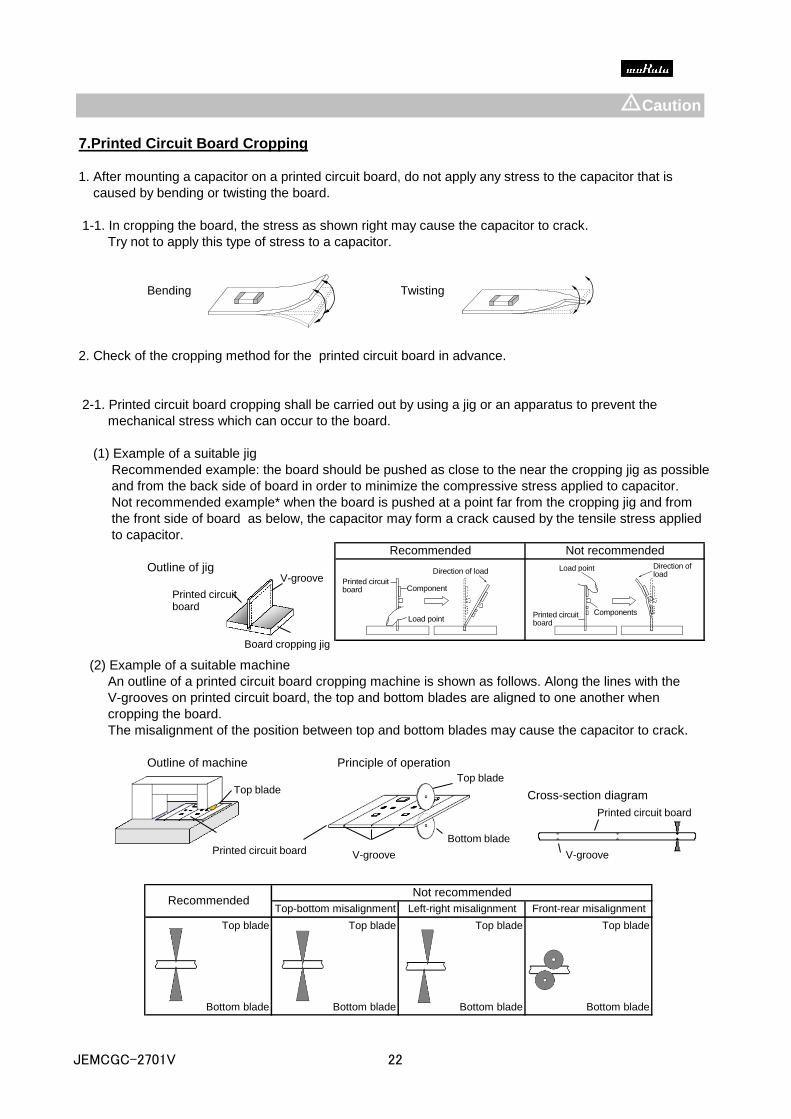
7.Printed Circuit Board Cropping
1. After mounting a capacitor on a printed circuit board, do not apply any stress to the capacitor that is
caused by bending or twisting the board.
1-1. In cropping the board, the stress as shown right may cause the capacitor to crack.
Try not to apply this type of stress to a capacitor.
Bending Twisting
2. Check of the cropping method for the printed circuit board in advance.
2-1. Printed circuit board cropping shall be carried out by using a jig or an apparatus to prevent the
mechanical stress which can occur to the board.
(1) Example of a suitable jig
Recommended example: the board should be pushed as close to the near the cropping jig as possible
and from the back side of board in order to minimize the compressive stress applied to capacitor.
Not recommended example* when the board is pushed at a point far from the cropping jig and from
the front side of board as below, the capacitor may form a crack caused by the tensile stress applied
to capacitor.
Outline of jig
(2) Example of a suitable machine
An outline of a printed circuit board cropping machine is shown as follows. Along the lines with the
V-grooves on printed circuit board, the top and bottom blades are aligned to one another when
cropping the board.
The misalignment of the position between top and bottom blades may cause the capacitor to crack.
Outline of machine Principle of operation
Cross-section diagram
Top blade Top blade Top blade Top blade
Bottom blade Bottom blade Bottom blade Bottom blade
Caution
RecommendedNot recommended
Top-bottom misalignment Left-right misalignment Front-rear misalignment
Recommended Not recommended
Printed circuit board
V-groove
Board cropping jig
Printed circuit board
Top blade
V-groove
Bottom blade
Top blade
Printed circuit board
V-groove
!
①
1A
Printed circuit board
Components
Load point
Direction of load
Printed circuit board
Components
Load point
Direction of load
JEMCGC-2701V 22

■ Others
1. Under Operation of Equipment
1-1. Do not touch a capacitor directly with bare hands during operation in order to avoid the danger of
a electric shock.
1-2. Do not allow the terminals of a capacitor to come in contact with any conductive objects (short-circuit).
Do not expose a capacitor to a conductive liquid, inducing any acid or alkali solutions.
1-3. Confirm the environment in which the equipment will operation is under the specified conditions.
Do not use the equipment under the following environment.
(1) Being spattered with water or oil.
(2) Being exposed to direct sunlight.
(3) Being exposed to Ozone, ultraviolet rays or radiation.
(4) Being exposed to toxic gas (e.g., hydrogen sulfide, sulfur dioxide, chlorine, ammonia gas etc.)
(5) Any vibrations or mechanical shocks exceeding the specified limits.
(6) Moisture condensing environments.
1-4. Use damp proof countermeasures if using under any conditions that can cause condensation.
2. Others
2-1. In an Emergency
(1) If the equipment should generate smoke, fire or smell, immediately turn off or unplug the equipment.
If the equipment is not turned off or unplugged, the hazards may be worsened by supplying
continuous power.
(2) In this type of situation, do not allow face and hands to come in contact with the capacitor or burns may be
caused by the capacitors high temperature.
2-2. Disposal of waste
When capacitors are disposed, they must be burned or buried by the industrial waste vender with
the appropriate licenses.
2-3. Circuit Design
GRM Series capacitors in this specification are not safety recognized products.
2-4. Remarks
Failure to follow the cautions may result, worst case, in a short circuit and smoking when
the product is used.
The above notices are for standard applications and conditions. Contact us when the products are
used in special mounting conditions.
Select optimum conditions for operation as they determine the reliability of the product after assembly.
The data herein are given in typical values, not guaranteed ratings.
Caution!
JEMCGC-2701V 23

■ Rating
1.Operating Temperature
1. The operating temperature limit depends on the capacitor.
1-1.Do not apply temperatures exceeding the upper operating temperature.
It is necessary to select a capacitor with a suitable rated temperature which will cover the operating
temperature range.
Also it is necessary to consider the temperature distribution in equipment and the seasonal temperature
variable factor.
1-2.Consider the self-heating of the capacitor
The surface temperature of the capacitor shall be the upper operating temperature or less when
including the self-heating factors.
2.Atmosphere surroundings (gaseous and liquid)
1. Restriction on the operating environment of capacitors.
1-1. The capacitor, when used in the above, unsuitable, operating environments may deteriorate
due to the corrosion of the terminations and the penetration of moisture into the capacitor.
1-2. The same phenomenon as the above may occur when the electrodes or terminals of the capacitor are
subject to moisture condensation.
1-3. The deterioration of characteristics and insulation resistance due to the oxidization or corrosion of
terminal electrodes may result in breakdown when the capacitor is exposed to corrosive or
volatile gases or solvents for long periods of time.
3.Piezo-electric Phenomenon
1. When using high dielectric constant type capacitors in AC or pulse circuits, the capacitor itself vibrates
at specific frequencies and noise may be generated.
Moreover, when the mechanical vibration or shock is added to capacitor, noise may occur.
Notice
JEMCGC-2701V 24
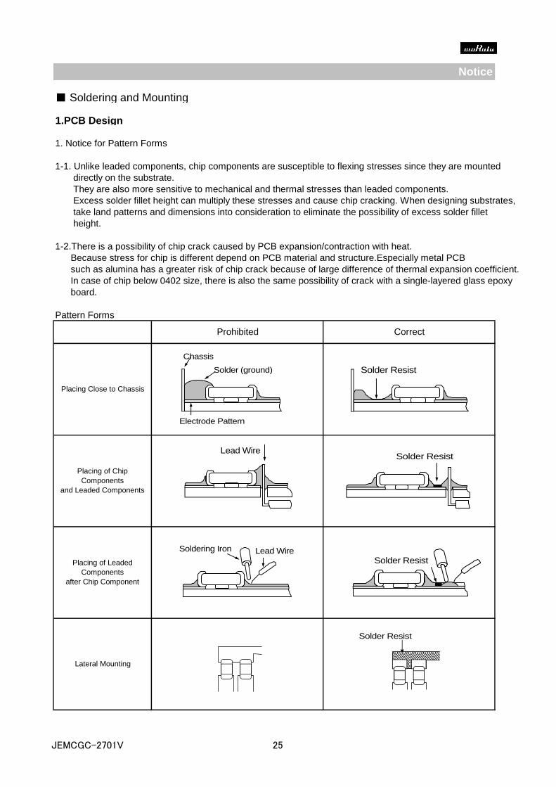
■ Soldering and Mounting
1.PCB Design
1. Notice for Pattern Forms
1-1. Unlike leaded components, chip components are susceptible to flexing stresses since they are mounted
directly on the substrate.
They are also more sensitive to mechanical and thermal stresses than leaded components.
Excess solder fillet height can multiply these stresses and cause chip cracking. When designing substrates,
take land patterns and dimensions into consideration to eliminate the possibility of excess solder fillet
height.
1-2.There is a possibility of chip crack caused by PCB expansion/contraction with heat.
Because stress for chip is different depend on PCB material and structure.Especially metal PCB
such as alumina has a greater risk of chip crack because of large difference of thermal expansion coefficient.
In case of chip below 0402 size, there is also the same possibility of crack with a single-layered glass epoxy
board.
Pattern Forms
Placing of Leaded
Components
after Chip Component
Lateral Mounting
Notice
Prohibited Correct
Placing Close to Chassis
Placing of Chip
Components
and Leaded Components
Chassis
Solder (ground)
Electrode Pattern
Solder Resist
Lead Wire
Solder Resist
Lead Wire Soldering Iron
Solder Resist
ソルダレジスト
Solder Resist
JEMCGC-2701V 25

2. Land Dimensions
2-1. Chip capacitor can be cracked due to the stress of PCB
bending / etc if the land area is larger than needed and has an excess
amount of solder.
Please refer to the land dimensions in table 1 for flow
soldering, table 2 for reflow soldering.
Please confirm the suitable land dimension by evaluating of the actual SET / PCB.
Table 1 Flow Soldering MethodDimensions
Part Number
GR□31 3.2×1.6 2.2~2.6 1.0~1.1 1.0~1.4
(in mm)
Table 2 Reflow Soldering MethodDimensions
Part Number
GR□02 0.4×0.2 0.16~0.2 0.12~0.18 0.2~0.23
GR□32 3.2×2.5 2.0~2.4 1.0~1.2 1.8~2.3
GR□43 4.5×3.2 3.0~3.5 1.2~1.4 2.3~3.0
GR□55 5.7×5.0 4.0~4.6 1.4~1.6 3.5~4.8
(in mm)
GR□21
1.9~2.1 1.0~1.3 1.7~1.9
2.0×1.25
(±0.15)1.2 0.6~0.8 1.2~1.4
GR□31
3.2×1.6
(within±0.20)1.8~2.0 0.9~1.2 1.5~1.7
3.2×1.6
(±0.30)
1.2~1.42.0×1.25
(±0.20)
0.9~1.0 0.8~1.1
GR□18
2.0×1.25
(within ±0.10)1.2 0.6 1.25
1.0~1.4 0.6~0.8
c
Notice
Chip(L×W) a b c
0.8~0.9 0.6~0.8
2.0×1.25 1.0~1.2GR□21
1.6×0.8 0.6~1.0
0.6×0.3 0.2~0.3 0.2~0.35
a
L×W
(Dimensions
Tolerance)
b
GR□03 0.2~0.4
0.3~0.5 0.35~0.45 0.4~0.6
1.6×0.8
(within ±0.10)
1.0×0.5
(±0.15/±0.20)0.4~0.6 0.40~0.50 0.5~0.7
GR□15
GR□181.6×0.8
(±0.15/±0.20)0.7~0.9 0.7~0.8 0.8~1.0
0.6~0.8 0.6~0.7 0.6~0.8
1.0×0.5
(within ±0.10)
Chip CapacitorLand
Solder Resistab
C
JEMCGC-2701V 26
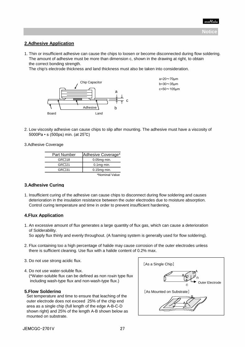
2.Adhesive Application
1. Thin or insufficient adhesive can cause the chips to loosen or become disconnected during flow soldering.
The amount of adhesive must be more than dimension c, shown in the drawing at right, to obtain
the correct bonding strength.
The chip's electrode thickness and land thickness must also be taken into consideration.
a=20~70μm
b=30~35μm
c=50~105μm
2. Low viscosity adhesive can cause chips to slip after mounting. The adhesive must have a viscosity of
5000Pa • s (500ps) min. (at 25℃)
3.Adhesive Coverage
Part Number Adhesive Coverage*GR□18 0.05mg min.
GR□21 0.1mg min.
GR□31 0.15mg min.
*Nominal Value
3.Adhesive Curing
1. Insufficient curing of the adhesive can cause chips to disconnect during flow soldering and causes
deterioration in the insulation resistance between the outer electrodes due to moisture absorption.
Control curing temperature and time in order to prevent insufficient hardening.
4.Flux Application
1. An excessive amount of flux generates a large quantity of flux gas, which can cause a deterioration
of Solderability.
So apply flux thinly and evenly throughout. (A foaming system is generally used for flow soldering).
2. Flux containing too a high percentage of halide may cause corrosion of the outer electrodes unless
there is sufficient cleaning. Use flux with a halide content of 0.2% max.
3. Do not use strong acidic flux.
4. Do not use water-soluble flux.
(*Water-soluble flux can be defined as non rosin type flux
including wash-type flux and non-wash-type flux.)
5.Flow Soldering Set temperature and time to ensure that leaching of the
outer electrode does not exceed 25% of the chip end
area as a single chip (full length of the edge A-B-C-D
shown right) and 25% of the length A-B shown below as
mounted on substrate.
Notice
Chip Capacitor
Board
Adhesive
Land
a
b
c
A
BD
COuter Electrode
[As a Single Chip]
[As Mounted on Substrate]
A
B
JEMCGC-2701V 27

Notice
6.Washing
1. Please evaluate a capacitor by actual cleaning equipment and condition surely
for confirming the quality and select the applicable solvent.
2. Unsuitable cleaning solvent may leave residual flux, other foreign substances, causing deterioration of
electrical characteristics and the reliability of the capacitors.
3. Select the proper cleaning conditions.
3-1. Improper cleaning conditions (excessive or insufficient) may result in the deterioration of the
performance of the capacitors.
7.Coating
1. A crack may be caused in the capacitor due to the stress of the thermal contraction of the resin during
curing process.
The stress is affected by the amount of resin and curing contraction.
Select a resin with small curing contraction.
The difference in the thermal expansion coefficient between a coating resin or a molding resin and
capacitor may cause the destruction and deterioration of the capacitor such as a crack or peeling, and
lead to the deterioration of insulation resistance or dielectric breakdown.
Select a resin for which the thermal expansion coefficient is as close to that of capacitor as possible.
A silicone resin can be used as an under-coating to buffer against the stress.
2. Select a resin that is less hygroscopic.
Using hygroscopic resins under high humidity conditions may cause the deterioration of the
insulation resistance of a capacitor.
An epoxy resin can be used as a less hygroscopic resin.
■ Others
1.Transportation
1. The performance of a capacitor may be affected by the conditions during transportation.
1-1. The capacitors shall be protected against excessive temperature, humidity and mechanical force
during transportation.
(1) Climatic condition
- low air temperature:-40℃ - change of temperature air/air:-25℃/+25℃ - low air pressure:30 kPa
- change of air pressure:6 kPa/min
(2) Mechanical condition
Transportation shall be done in such a way that the boxes are not deformed and forces are not directly
passed on to the inner packaging.
1-2. Do not apply excessive vibration, shock, and pressure to the capacitor.
(1) When excessive mechanical shock or pressure is applied to a capacitor, chipping or cracking may
occur in the ceramic body of the capacitor.
(2) When a sharp edge of an air driver, a soldering iron, tweezers, a chassis, etc. impacts strongly on the
surface of capacitor, the capacitor may crack and short-circuit.
1-3. Do not use a capacitor to which excessive shock was applied by dropping etc. The capacitor dropped accidentally during processing may be damaged.
JEMCGC-2701V 28
NOTE
1.Please make sure that your product has been evaluated in view of your specifications with our
product being mounted to your product.
2.Your are requested not to use our product deviating from this product specification.
3.We consider it not appropriate to include any terms and conditions with regard to the business
transaction in the product specifications, drawings or other technical documents. Therefore,
if your technical documents as above include such terms and conditions such as warranty clause,
product liability clause, or intellectual property infringement liability clause, they will be deemed to
be invalid.
!
JEMCGC-2701V 29


