
Chinese Journal of Physics - umexpert.um.edu.my · ... in wide band-gap II–VI and III–V...
12
Chinese Journal of Physics 55 (2017) 1032–1043 Contents lists available at ScienceDirect Chinese Journal of Physics journal homepage: www.elsevier.com/locate/cjph Optical properties of (Pb 1- x Mn x S) 1- y Fe y materials from first-principles calculations H. Belhadj a , M. Ameri b,∗ , B. Abbar a , N. Moulay b , A.Z. Bouyakoub b , O. Arbouche b , D. Bensaid b , I. Ameri c , S. Mesbah b , Y. Al-Douri c a Laboratoire de Modélisation et de Simulation en Sciences des Matériaux Département, Physique Université Djillali Liabès, Sidi Bel-Abbes, Algeria (LMSSM) b Laboratory of Physical Chemistry of Advanced Materials (LPCMA), University of Djillali Liabes, BP 89, Sidi-Bel-Abbes 22000, Algeria c Physics Department, Faculty of Science, University of Sidi-Bel-Abbes, 22000, Algeria a r t i c l e i n f o Article history: Received 25 September 2016 Revised 31 October 2016 Accepted 27 November 2016 Available online 23 March 2017 Keywords: L/APW+lo MBJ-GGA+U Lead/iron chalcogenides Photovoltaics Infrared lasers Optical properties a b s t r a c t A theoretical study of the optical properties of Pb 0.25 Mn 0.25 S, Pb 0.25 Fe 0.25 S, Pb 0.25 Mn 0.125 Fe 0.125 S in the framework of the density functional theory using the linearized- augmented plane-wave method is reported in order to predict new optical materials for continuous-wave lasers. The electronic structure of all lead/iron chalcogenides (LICs)is studied in the zircon-type structure. The DFT + U (Hubbard parameter) with U= 8 eV predicts an anti-ferromagnetic and nonmagnetic insulating ground states—at ambient conditions—for (Pb 0.25 Mn 0.25 S, Pb 0.25 Fe 0.25 S) and Pb 0.25 Mn 0.125 Fe 0.125 S, respectively. The results show that these LICs can be good candidats for laser-host materials and indicate the possibility of a material design to optimize this kind of materials. The rare-earth ion-doped crystals could enhance the laser performances and improve the isolation characteristic of the optical isolators. © 2017 The Physical Society of the Republic of China (Taiwan). Published by Elsevier B.V. All rights reserved. 1. Introduction Lead chalcogenides PbX (where X can be elements such as S, Se, and Te), as narrow gap semiconducting IV–VI com- pounds have been extensively studied by experiments over the past several decades due to their potential applications as electronic devices. They have attracted great theoretical interest aimed at understanding the physics of their phase transi- tions, electronic band gaps, and ferroelectric like behavior at low temperatures, exhibiting outstanding optical and electrical transport properties [1]. Nanoscale IV–VI lead chalcogenides have been an intensive research interest because of their po- tential applications in sensors, lasers, solar cells, infrared detectors, thermoelectric cooling materials, etc. [2]. They are very useful substances for optoelectronic devices in the infrared (IR) region of the spectrum [3]. Lead salt PbS is a family member of the lead chalcogenides, employed in photo-detectors and recognized as a promising material for photovoltaics, it has sev- eral unique properties, such as a high dielectric constant (190) and a large exciton Bohr radius (20 nm) [4]. It is also widely used as a material for tunable laser devices [5]. PbS has an experimental refractive index, as a function of photon energy in the increasing wavelength range 3.10–4.96 μm, decreasing from 4.30 to 4.10 [6], and a narrow direct band-gap (strongly temperature dependent) of 0.41 eV at 300 K [7]. ∗ Corresponding author. E-mail addresses: [email protected], [email protected] (M. Ameri). http://dx.doi.org/10.1016/j.cjph.2016.11.015 0577-9073/© 2017 The Physical Society of the Republic of China (Taiwan). Published by Elsevier B.V. All rights reserved.
Transcript of Chinese Journal of Physics - umexpert.um.edu.my · ... in wide band-gap II–VI and III–V...

Chinese Journal of Physics 55 (2017) 1032–1043
Contents lists available at ScienceDirect
Chinese Journal of Physics
journal homepage: www.elsevier.com/locate/cjph
Optical properties of (Pb 1- x Mn x S) 1- y
Fe y
materials from
first-principles calculations
H. Belhadj a , M. Ameri b , ∗, B. Abbar a , N. Moulay
b , A.Z. Bouyakoub
b , O. Arbouche
b , D. Bensaid
b , I. Ameri c , S. Mesbah
b , Y. Al-Douri c
a Laboratoire de Modélisation et de Simulation en Sciences des Matériaux Département, Physique Université Djillali Liabès, Sidi Bel-Abbes,
Algeria (LMSSM) b Laboratory of Physical Chemistry of Advanced Materials (LPCMA), University of Djillali Liabes, BP 89, Sidi-Bel-Abbes 220 0 0, Algeria c Physics Department, Faculty of Science, University of Sidi-Bel-Abbes, 220 0 0, Algeria
a r t i c l e i n f o
Article history:
Received 25 September 2016
Revised 31 October 2016
Accepted 27 November 2016
Available online 23 March 2017
Keywords:
L/APW + lo
MBJ-GGA + U
Lead/iron chalcogenides
Photovoltaics
Infrared lasers
Optical properties
a b s t r a c t
A theoretical study of the optical properties of Pb 0.25 Mn 0.25 S, Pb 0.25 Fe 0.25 S,
Pb 0.25 Mn 0.125 Fe 0.125 S in the framework of the density functional theory using the linearized-
augmented plane-wave method is reported in order to predict new optical materials for
continuous-wave lasers. The electronic structure of all lead/iron chalcogenides (LICs)is
studied in the zircon-type structure. The DFT + U (Hubbard parameter) with U = 8 eV
predicts an anti-ferromagnetic and nonmagnetic insulating ground states—at ambient
conditions—for (Pb 0.25 Mn 0.25 S, Pb 0.25 Fe 0.25 S) and Pb 0.25 Mn 0.125 Fe 0.125 S, respectively. The
results show that these LICs can be good candidats for laser-host materials and indicate
the possibility of a material design to optimize this kind of materials. The rare-earth
ion-doped crystals could enhance the laser performances and improve the isolation
characteristic of the optical isolators.
© 2017 The Physical Society of the Republic of China (Taiwan). Published by Elsevier B.V.
All rights reserved.
1. Introduction
Lead chalcogenides Pb X (where X can be elements such as S, Se, and Te), as narrow gap semiconducting IV–VI com-
pounds have been extensively studied by experiments over the past several decades due to their potential applications as
electronic devices. They have attracted great theoretical interest aimed at understanding the physics of their phase transi-
tions, electronic band gaps, and ferroelectric like behavior at low temperatures, exhibiting outstanding optical and electrical
transport properties [1] . Nanoscale IV–VI lead chalcogenides have been an intensive research interest because of their po-
tential applications in sensors, lasers, solar cells, infrared detectors, thermoelectric cooling materials, etc. [2] . They are very
useful substances for optoelectronic devices in the infrared (IR) region of the spectrum [3] . Lead salt PbS is a family member
of the lead chalcogenides, employed in photo-detectors and recognized as a promising material for photovoltaics, it has sev-
eral unique properties, such as a high dielectric constant (190) and a large exciton Bohr radius (20 nm) [4] . It is also widely
used as a material for tunable laser devices [5] . PbS has an experimental refractive index, as a function of photon energy
in the increasing wavelength range 3.10–4.96 μm, decreasing from 4.30 to 4.10 [6] , and a narrow direct band-gap (strongly
temperature dependent) of 0.41 eV at 300 K [7] .
∗ Corresponding author.
E-mail addresses: [email protected] , [email protected] (M. Ameri).
http://dx.doi.org/10.1016/j.cjph.2016.11.015
0577-9073/© 2017 The Physical Society of the Republic of China (Taiwan). Published by Elsevier B.V. All rights reserved.

H. Belhadj et al. / Chinese Journal of Physics 55 (2017) 1032–1043 1033
Paramagnetic doping (Mn
2 + , Fe 3 + , etc.) in wide band-gap II–VI and III–V compounds has been largely explored to tailor
their physical properties both in bulk and nanostructures and hence a large interest lies in such doped II–VI and III–V
semiconductor (SC) nanostructures for the realization of photonic and spintronic devices [8-10] . Mn
2 + ions are chosen as
the dopants because ( i ) their half-filled d orbital yields a maximum sp −d exchange interaction with the conduction electrons,
and ( ii ) Mn
2 + ions act neither as donors nor as acceptors in PbS if Mn
2 + substitutes Pb 2 + and thus will not affect the carrier
type and concentration in PbS [4] .
PbS has been alloyed with many other binary sulphides (like MnS and FeS) to form variable band gap ternary SCs such as
Pb 1 −x Mn x S to achieve variation in the band gap over large values; considering the band gaps of PbS (bulk) and MnS (bulk) as
0.41 and 3.5 eV, respectively, a bulk ternary alloy of the type Pb 1 −x Mn x S should show a variation of the bandgaps between
the limiting values of 0.41 and 3.5 eV [11] .Pb 1–x Mn x S crystallizes in the NaCl structure (space group: O
5 h
– Fm3m) and has
a lattice constant decreasing linearly with x (from solid solutions reported up to 0.05) [12] . Joshi et al. [13] have deposited
single-phase nanoparticle thin films of ternary Pb 1 −x Mn x S materials on different substrates, and found that optical band gap
in Pb 1 −x Mn x S varied from 1.65 to 1.42 eV by changing x in the range of 0.25 < x < 0.75. A small amount of Mn ions in the
PbS lattice causes an increase of the energy bandgap compared to PbS. For example, the stimulated emission wavelength of
Pb 0.986 Mn 0.014 S laser 3.87 μm is lower than the wavelength of the PbS laser 4.31 μm at the same temperature; the bandgap
of this material remains direct, as in PbS [14] . For terawatt-scale thin film photovoltaics, earth abundant absorber materials
are the most promising candidates due to the robust supply chains for the elements involved, so that the potential material
systems, FeS 2 and PbS, are just beginning to be re-examined with solution phase processing [15] .
As for the iron chalcogenides Fe X , they are of particular interest because of their interesting magnetic, semiconducting,
and structural properties [16–18] . Consequently they have been targeted for potential use in biomedical applications, in-
cluding protein immobilization and separation [19] , magnetic targeting and drug delivery [20–22] ,cancer hyperthermia [23] ,
magnetic resonance imaging [24–26] , etc. Iron sulfide (FeS), particularly the pyrite phase FeS 2 having properties suitable for
photovoltaics, is of considerable interest in solar applications and lithium batteries due to its low cost, favorable band gap
(0.95 eV), and high light absorption (6 × 10 5 cm
2 /mol), [27] FeS has a hexagonal structure with an energy gap of 0.04 eV in
the bulk phase and p -type conduction; when mixed with PbS, the resulting bulk Pb 1 −x Fe x S ternary alloys are likely to have
energy band gap values between 0.04 and 0.41 eV [28,29] .
Joshi et al. [30] have grew Pb 1 −x Fe x S nanoparticle films and reported that their optical band gap Eg N was observed to
decrease with an increase in the iron concentration x in the films. Eg N values for x = 0.25, 0.50 and 0.75 respectively of
1.65, 1.51 and 1.42 eV, suggest alloying between FeS with PbS to form the ternary Pb 1- x Fe x S, all nanoparticles. In Pb 1- x Fe x S
nanoparticle films, the larger optical band gap like that reported for PbS nanoparticles [31–33] is attributed to the quan-
tum confinement effect [34,35] . Tuning the optical and electrical properties of Pb 1 −x Fe x S (and maybe also Pb 1 −x Mn x S) by
controlling the size and material composition makes the PbS-based ternaries (and quaternaries) interesting candidates for
optoelectronic devices [36] .
The design and synthesis of high-efficiency materials to convert solar to electrical energy is becoming an increasingly
important research field [37] ; using first-principles electronic structure calculations we try in this work to design chalco-
genide photovoltaic absorbers, from Pb 1- x Mn x Sternary to (Pb 1- x Mn x S) 1- y Fe y quaternary compounds by predicting their optical
properties, in order to overcome the scarcity and high cost of indium and gallium in Cu(In,Ga)(S,Se) 2 based cells and the
high toxicity of cadmium in CdTe based cells. Zinc-blende chalcogenide SCs have been widely studied for photovoltaic ap-
plications [38] . Although these chalcogenides have shown some promising properties, it is important to develop systematic
design principles that accelerate the discovery of novel materials with lower cost and higher efficiency to satisfy the need
for wide-range photovoltaic applications [39–41] .
This paper is organized as follows: in Section 2 , we present the method of calculation, Section 3 contains all the results
and discussions, and finally we finish with a summary and conclusion in Section 4.
2. Methodology
The calculations have been performed within the DFT implemented in the Wien2 k code [42] .Atoms were represented
by the hybrid full-potential (linear) augmented plane wave plus local orbitals (L/APW + lo ) method [43] . In this method,
the wave functions, charge density and potential are expanded in spherical harmonics within non-overlapping muffin-tin
spheres, and plane waves are used in the remaining interstitial region of the unit cell. In the code, the core and valence
states are treated differently. Core states are treated within a multiconfiguration relativistic Dirac–Fock
Approach, while valence states are treated in a scalar relativistic approach. For the exchange-correlation energy we used
the GGA + U approach [44] . In order to overcome the underestimation on the band gaps from the common GGA approxi-
mation, we have used the newly suggested and most reliable technique called the modified Becke–Johnson (mBJ) potential
approximation [51] . Very carefully, step analysis is done to ensure convergence of the total energy in terms of the varia-
tional cutoff-energy parameter. At the same time, we have used an appropriate set of k -points to compute the total energy.
We compute the equilibrium lattice constants and bulk moduli by fitting the total energy versus volume to the Murnaghan
equation [52] . The total energy was minimized using a set of 10 k -points in the irreducible sector of the Brillouin zone,
equivalent to a6 × 6 × 6 Monkhorst–Pack [53] grid in the unit cell, and the value of 7 Ry for the cutoff energy was used. The
self-consistent calculations are considered to be converged only when the calculated total energy of the crystal converged
to less than 1 mRy. We have adopted the values of 2.5, 2.2, 2.3, and 1.6 Bohr respectively for the Pb, Mn, S and Fe atoms,

1034 H. Belhadj et al. / Chinese Journal of Physics 55 (2017) 1032–1043
Table 1
Calculated lattice constants and bulk modulus for PbS, Pb 0.25
Mn 0.25 S and Pb 0.25 Fe 0.25 S using the GGA and GGA + U.
Compounds Approximation a 0 ( ̊A) B 0 (Gpa) B’
PbS GGA 6.019 53.982 3.980
Pb 0.25 Mn 0.25 S GGA 5.886 55.930 4.370
GGA + U 5.902 55.823 4.711
Pb 0.25 Fe 0.25 S GGA 5.860 57.147 3.314
GGA + U 5.882 56.378 4.745
Fig. 1. Crystal structure of Pb 0.25 Mn 0.125 Fe 0.125 S.
as muffin tin radii. The density of states has been calculated using the linear tetrahedron method with Blöchl corrections
[54] . The supercell is made by multiples of the lattice vectors a , b , c , like the 64-atoms supercell for the Rock-salt phase. The
exchange-correlation energy was calculated using the GGA + U approach [44] (U = 0.25Ry). The analysis is done to ensure the
convergence of the total energy in terms of the variational cutoff-energy parameter. On the other hand, we have used an
appropriate set of k points to compute the total energy. The standard built-in basis functions were applied with the valence
configurations of (Pb: 5s 2 5p
6 4f 7 5d
1 6s 2 , S: 5s 2 5p
6 4f 11 5d
1 6s 2 , Mn: 5s 2 5p
6 4f 14 5d
1 6s 2 ) and (Fe: 3s 2 3p
6 3d
3 4s 2 ). The
total energy was minimized using a set of 150, 163 and 163 k -points in the irreducible sector of the Brillouin zone for the
LICsPb 0.25 Mn 0.25 S, Pb 0.25 Fe 0.25 S and Pb 0.25 Mn 0.125 Fe 0.125 S, respectively, and the value of 7 for the cutoff energy was used. In
fact, the DFT method has proven to be one of the most accurate methods for the computation of the electronic structure of
solids [45–50] , which our compounds are.
3. Results and discussion
3.1. Electronic properties and magnetism of Pb 1 −x Mn x S and Pb 1 −x Fe x S
In this work, the electronic structure and magnetic interactions of Mn and Fe substituting in cubic PbS are studied. Our
calculations were performed on the rock salt ferromagnetic phase, at the concentration x = 0.25, where Mn is substituted
toPb in PbMnS and Fe is substituted to Pb in PbFeS. We have reported the spin-polarized band structures and the density
of states. The calculated lattice constants and bulk modulus in both phases are presented in Table 1 . Generally, the results
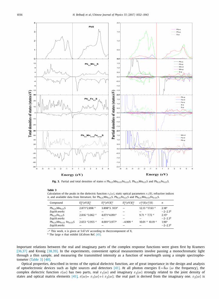
are in reasonable agreement with the experimental values ( Fig. 1 ).
Figs. 2 and 3 present the pictures of the calculated band structure and total and partial densities of states of
Pb 0.25 Mn 0.125 Fe 0.125 S and PbS, Pb 0.25 Mn 0.125 Fe 0.125 S, Pb 0.25 Mn 0.25 S, Pb 0.25 Fe 0.25 S, respectively. One can see the presence of
a gap above the Fermi level in all the compounds. The calculated results obtained for the doped compounds Pb 0.25 Mn 0.25 S
and Pb 0.25 Fe 0.25 Sshows that the total magnetic moments are very similar for both approximations (GGA and GGA + U). The
spin magnetic moment of Pb, S atoms varies in different doped compounds from 0.006μB to 0.021μB for the Pb atom and
from 0.047 μB to 0.085 μB for S atom using GGA. And from0.001 μB to 0.002 μB for Pb and from 0.005 μB to 0.009 μB for
the S using the GGA + U. In the case of Pb 0.25 Mn 0.25 S, the Mn atoms are randomly distributed on the crystallographic posi-
tions and they behave a magnetic impurities in the nonmagnetic(NM) states. The magnetic Mn atom enters the NM state
in the ferromagnetic(FM) state. Therefore, the Mn atoms behave as a magnetic impunity in PbS. The replacement of a Mn
atom with a Pb atom leads to FM-like behavior in this system but slightly smaller ( Table 2 ). By describing the response of a
medium to applied the electromagnetic radiation within the framework of the linear response theory, the optical properties
of a material change or affect the characteristics of light passing through it by modifying its propagation vector or intensity.

H. Belhadj et al. / Chinese Journal of Physics 55 (2017) 1032–1043 1035
Fig. 2. (a) Spin down/up energy bands of Pb 0.25 Mn 0.125 Fe 0.125 S. (b) Spin down/ dnenergy bands of Pb 0.25 Mn 0.125 Fe 0.125 S.
Table 2
Calculated total and local magnetic moments (in μB ) within the muffin-tin spheres
and in the interstitial sites for Pb 0.25 Mn 0.25 S and Pb 0.25 Fe 0.25 S using the GGA and
GGA + U.
Compounds Approximation Tot Pb Mn Fe S
Pb 0.25 Mn 0.25 S GGA 4.997 0.006 4.664 – 0.047
GGA + U 4.999 0.001 4.902 – 0.005
Pb 0.25 Fe 0.25 S GGA 4.044 0.021 – 3.579 0.085
GGA + U 4.002 0.002 – 3.931 0.009
1036 H. Belhadj et al. / Chinese Journal of Physics 55 (2017) 1032–1043
Fig. 3. Partial and total densities of states o Pb 0.25 Mn 0.125 Fe 0.125 S, Pb 0.25 Mn 0.25 S and Pb 0.25 Fe 0.25 S.
Table 3
Calculation of the peaks in the dielectric function ε2 ( ω), static optical parameters ε1 (0), refractive indices
n , and available data from literature, for Pb 0.25 Mn 0.25 S, Pb 0.25 Fe 0.25 S and Pb 0.25 Mn 0.125 Fe 0.125 S.
Compound E xx 0 (eV) E zz
0 E xx 1 (eV) E zz
1 E xx 2 (eV) E zz
2 ε xx 1 (0) ε zz
1 (0) n
Pb 0.25 Mn 0.25 S 2.871 a 2.898 a 3.898 a 3. 933 a — 12.13 a 17.63 a 2.18 a
Exp/th.works — — — — ∼2–2.3 b
Pb 0.25 Fe 0.25 S 2.816 a 3.062 a 4.071 a 4.091 a — 9.71 a 7.72 a 2.15 a
Exp/th.works — — — — ∼2–2.3 b
Pb 0.25 Mn 0.125 Fe 0.125 S 2.653 a 2.955 a 4.001 a 3.977 a –4.909 a 10.01 a 10.19 a 1.96 a
Exp/th.works — — — — ∼2–2.3 b
–a This work, n is given at 5.67 eV according to the zz component of X, b The large n that exhibit LICsfrom Ref. [45] .
Important relations between the real and imaginary parts of the complex response functions were given first by Kramers
[36,37] and Kronig [38,39] . In the experiments, convenient optical measurements involve passing a monochromatic light
through a thin sample, and measuring the transmitted intensity as a function of wavelength using a simple spectropho-
tometer ( Table 3 ) [40] .
Optical properties, described in terms of the optical dielectric function, are of great importance in the design and analysis
of optoelectronic devices such as light sources and detectors [41] . At all photon energies E = ̄h ω ( ω the frequency), the
complex dielectric function ε( ω) has two parts, real ε1 ( ω) and imaginary ε2 ( ω) strongly related to the joint density of
states and optical matrix elements [41] , ε( ω) = ε ( ω) + i ε ( ω); the real part is derived from the imaginary one. ε ( ω) is
1 2 2
H. Belhadj et al. / Chinese Journal of Physics 55 (2017) 1032–1043 1037
Fig. 4. Real ε1 and imaginary ε2 parts of the dielectric functions of Pb 0.25 Mn 0.125 Fe 0.125 S, Pb 0.25 Mn 0.25 S and Pb 0.25 Fe 0.25 S.
an essential quantity indicating the various interband transitions in a SC. There are two contributions to ε( ω), interband
and intraband transitions. We neglect the indirect interband transitions which involve the scattering of phonons and are
expected to give a small contribution to ε ( ω) [42] . Fig. 4 shows that ε2 ( ω) is characterized by a single peak structure
(beyond the fundamental gap energies) for Pb 0.25 Mn 0.25 S and Pb 0.25 Fe 0.25 S ( ε xx 2
): E 1 = 3.334 and 3.714 eV respectively, and a
two peak structure for Pb 0.25 Mn 0.125 Fe 0.125 S( ε zz 2
): (E 1 , E 2 ) = 0.8843, 1.455 eV.
The electronic properties of a SC are primarily determined by intraband transitions, which describe the transport of car-
riers in real space. Optical properties are meanwhile connected with these interband transitions, so that a strict separation
is impossible. Hence, the optical and electronic SC properties are intimately related and should be discussed jointly [43] . In
order to well understand the optical transitions phenomenon in our SC LICs, we give in Table 1 the peaks in the dielectric
function ε2 ( ω), static optical parameters ε1 (0) and refractive indices n zz at 5.67 eV near the upper limit of the energy range
experimentally exploited, compared to the available data in the literature.
3.2. Refractive index and extinction coefficient
The two most important optical properties of a material are its refractive index n and extinction coefficient (or attenu-
ation index) K . n , the most important optical constant, depends in general on the wavelength of the electromagnetic wave,
through dispersion relations denoting the frequency or wavelength dependence of n and K . In materials where an electro-
magnetic wave can lose its energy during its propagation, the refractive index becomes complex. Its real and imaginary parts
are respectively n and K [40] , usually used for the propagation and dissipation of electromagnetic waves in a medium [44] .
Given the material parameters such as the dielectric constant ε1 , the conductivity σ 1 , and the permeability μ1 denoting the
charge of the electric and magnetic fields and current when matter is present, the complex refractive index as a response
function describing the optical properties of the medium is defined as follows [44] :
−N
= n + ik =
[ ε
1 μ
1 + i
4 πμ1 σ
1
ω
] 1 / 2 =
[ −ε μ
1
] 1 / 2 (1)
where n and k are completely determined by σ 1 , μ1 , and ε1 [44] :
−n
2 =
μ1
2
{ [ε 2
1 +
(4 πσ
1
ω
)2 ]1 / 2
+ ε 1
}
and
−k 2 =
μ1
2
{ [ε 2
1 +
(4 πσ
1
ω
)2 ]1 / 2
− ε 1
}
. (2)

1038 H. Belhadj et al. / Chinese Journal of Physics 55 (2017) 1032–1043
Fig. 5. Refractive indexes and extinctions coefficients of Pb 0.25 Mn 0.125 Fe 0.125 S, Pb 0.25 Mn 0.25 S and Pb 0.25 Fe 0.25 S.
These two important relations contain all the information on the propagation of the electromagnetic wave in the material.
ε1 , μ1 , and σ 1 are given in terms of n and k:
n
2 − k 2 = ε 1 μ
1 and 2 nk =
4 πμ1 σ
1
ω
. (3)
and the complex refractive index, given in Eq.(1) , can be written as
−N
2 = μ1
[ ε
1 + i
4 πσ1
ω
] = μ
1
−ε �
4 π i μ1
−σ
ω
. (4)
As mentioned above, the refractive index n ( ω) of a SC is a very important physical parameter related to the microscopic
atomic interactions; its knowledge turns out to be of fundamental importance in optoelectronics [42] . The crystal can be
considered as a collection a of electric charges, n ( ω) will then be related to the local polarization of these entities. It can be
described in terms of the complex dielectric function as [42]
n (ω) =
√
ε 1 (ω) +
√
ε 2 1 (ω) + ε 2
1 (ω)
√
2
(5)
with regard to k :
k (ω) =
√
−ε 1 (ω) +
√
ε 2 1 (ω) + ε 2
1 (ω)
√
2
. (6)
In Fig. 5 , we present n over the range experimentally exploited ≤ 6 eV, where the dispersion is normal. Experimentaly, the
LICs exhibit large refractive indices ( ∼2–2.3), a birefringence ( ∼0.22) and effectively no IR absorption (1.5–2.5 μm) [45] .
Here according to the zz component of X, the common photon energy around 5.7 eV corresponds to a refractive index of
about 2,which yields a reflectivity of 0.16 and implies an extinction index of the same order corresponding to an absorption
coefficient larger than 2.5.10 5 cm
−1 .
3.3. Reflectivity
The experimental measurement of the reflectivity is easy, and the principal requirement is the availability of a reasonably
pure single crystal or polycrystalline material capable of having a face polished with a minimum surface area [52] . Several

H. Belhadj et al. / Chinese Journal of Physics 55 (2017) 1032–1043 1039
Fig. 6. Reflectivity of Pb 0.25 Mn 0.125 Fe 0.125 S, Pb 0.25 Mn 0.25 S and Pb 0.25 Fe 0.25 S.
methods can be employed to determine the optical constants from the measured reflectivity [53,54] . Alternatively, a direct
calculation of the optical constants can be obtained by a Kramers–Kronig analysis of the data [36–39] . Here it is more
essential that the absolute reflectivity be known accurately. This approach has more generally been used when the reflection
spectrum is more complex, as in the ultraviolet region. The reflectivity R of radiation incident normally on a semi-infinite
slab of an absorbing material is related to the complex index of refraction by Eq. (7) . In analogy with the situation in a
nonabsorbing medium where n = ε1 / 2 (both n and εreal ), in an absorbing medium the same relation can be used with both−N
and
−ε complex, where n is the ordinary index of refraction and k is the extinction coefficient. The optical reflectivity R( ω)
in the special configuration of normal incidence can be expressed as
R (ω) =
∣∣∣∣∣1 − −N
1 +
−N
∣∣∣∣∣2
=
∣∣∣∣ ( ε 1 (ω) + i ε 2 (ω)) 1 / 2 − 1
( ε 1 (ω) + i ε 2 (ω)) 1 / 2 + 1
∣∣∣∣2
=
(1 − n ) 2 + k 2
(1 + n ) 2 + k 2
. (7)
For a dielectric material without losses (the extinction coefficient k → 0), the normal-incidence reflectivity is solely deter-
mined by the refractive index:
R (ω) =
(1 − n
1 + n
)2
, (8)
and it can approach unity if n is large. This other very important parameter (deduced by the refracive index) characterizes
the reflective energy part of the interface of the solid, and depends on the incident photon energy. Main peaks in the
reflectivity spectrum correspond to interband transitions [40] . Fig. 6 shows the behavior of the reflectivity in dependence
on the photon energy for the three compounds. The main peaks of the reflectivity spectrum corresponding to interband
transitions are 3.41, 3.66, 4.66 eV and 3.877, 10.76 eV and 0.884, 1.510,3.877 eV, respectively for Pb 0.25 Mn 0.25 S, Pb 0.25 Fe 0.25 S
and Pb 0.25 Mn 0.125 Fe 0.125 S (according to the xx component of Z) and they decrease with increasing energy.
3.4. Optical conductivity
The complex dielectric constant −ε = ε 1 + i
4 πσ1 ω = ε 1 + i ε 2 and the optical conductivity
−σ = σ1 + i σ2 are related to each
other through
−ε = 1 +
4 π i −σ � 1 ⇒ σ (ω) = − iω
ε(ω) . (9)
ω 4 π
1040 H. Belhadj et al. / Chinese Journal of Physics 55 (2017) 1032–1043
Fig. 7. Real optical conductivity σ xx , σ zz of Pb 0.25 Mn 0.125 Fe 0.125 S, Pb 0.25 Mn 0.25 S and Pb 0.25 Fe 0.25 S.
We have calculated σ ( ω) over an energy range ≤ 15 eV In Fig. 7 , we show the optical conductivity spectra where several
peaks corresponding to the bulk plasmon excitations, which are caused by electrons crossing from the valence to the con-
duction band, are represented. Values of the optical conductivity in the high energy range (beyond 5 eV) and low energy
range (0.484 – 4.34 eV) correspond to the interband and intraband transitions, respectively. There is a single sharp peak in
the low energy range and several small peaks in the high energy range for all LICs compounds. The main peaks positions
are localized at 3.360, 8.367 and 10.13 eV and 3.877,10.762 eV and 0.884, 1.510 and 3.877 eV (according to the xx component
of Z) for Pb 0.25 Mn 0.25 S, Pb 0.25 Fe 0.25 S and Pb 0.25 Mn 0.125 Fe 0.125 S, respectively.
3.5. Electron energy loss function
The electron energy-loss function, L( ω), describes the interaction by which energy is lost by a fast moving electron trav-
elling throughout the material. Interactions may include phonon excitation, interband and intraband transitions, plasmon
excitations, inner shell ionizations and Cerenkov radiations. If both parts of the optical conductivity are such that σ 1 >> | σ 2 |,
the reflectivity R → 1. Usually large at the plasma frequency, L( ω)of the fast electrons moving in the mediumis [49]
L (ω) = Im [ −1 /ε(ω) ] =
ε 2 (ω)
ε 2 1 (ω) + ε 2
2 (ω)
. (10)
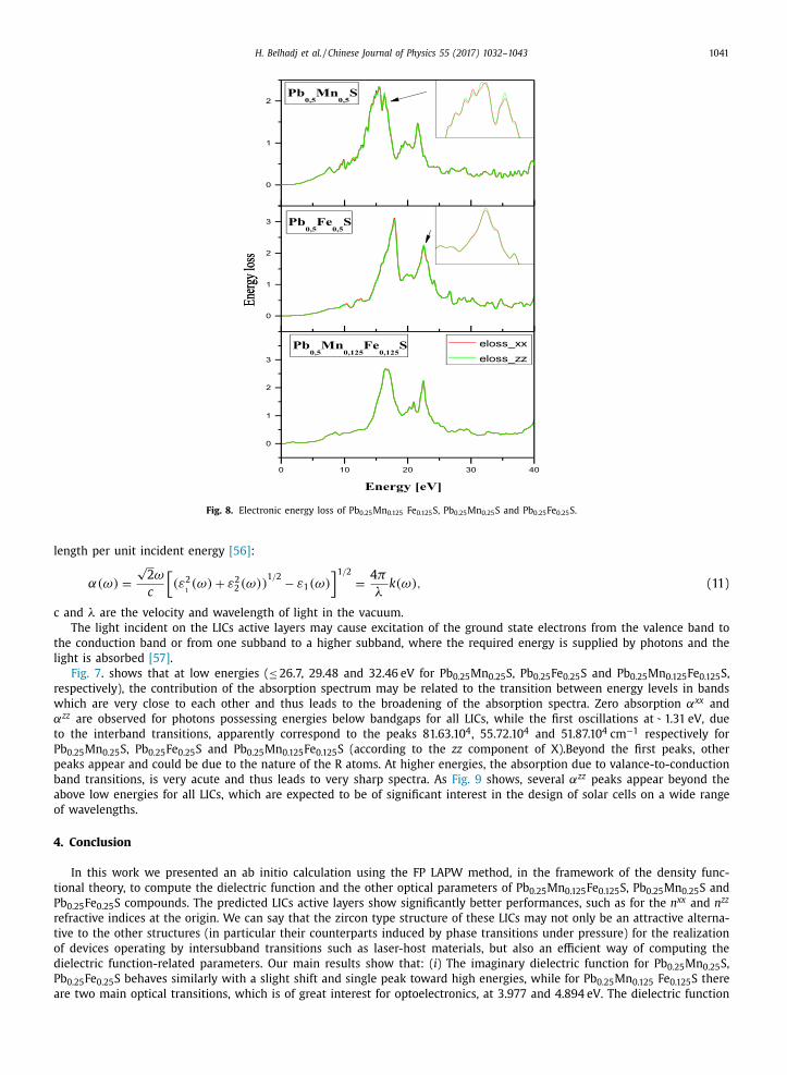
This function is the basic parameter measured by the electron loss spectroscopy. The most prominent peak in L( ω) is iden-
tified as the plasmon peak, signaling the energy of collective excitations of the electronic charge density in the crystal. As
displayed in Fig. 8 , the highest peak positions for L xx ( ω) were calculated at 15.524, 16.340,21.512 eV and 17.891, 22.517 and
16.911, 22.463 eV, respectively, for Pb 0.25 Mn 0.25 S, Pb 0.25 Fe 0.25 S and Pb 0.25 Mn 0.125 Fe 0.125 S. The sharp maximum in the energy-
loss function is associated with the existence of plasma oscillations. In comparison to the other physical quantities, the main
peaks of L( ω) are clear.
3.6. Absorption coefficient
The absorption related to transitions between the occupied and unoccupied states is caused by excitations due to the
interaction of photons and electrons. Optical absorption is due to the interband transition and intraband transition (Drude
term) [55,56] . The peak positions in the absorption spectrum correspond to the peaks of ε2 ( ω). Using both parts of ε( ω),
the optical absorption coefficient α( ω) characterizing such a phenomenon, is defined as the light energy absorbed in unit
H. Belhadj et al. / Chinese Journal of Physics 55 (2017) 1032–1043 1041
Fig. 8. Electronic energy loss of Pb 0.25 Mn 0.125 Fe 0.125 S, Pb 0.25 Mn 0.25 S and Pb 0.25 Fe 0.25 S.
length per unit incident energy [56] :
α(ω) =
√
2 ω
c
[ (ε 2
1 (ω) + ε 2 2 (ω))
1 / 2 − ε 1 ( ω) ] 1 / 2
=
4 π
λk ( ω) , (11)
c and λ are the velocity and wavelength of light in the vacuum.
The light incident on the LICs active layers may cause excitation of the ground state electrons from the valence band to
the conduction band or from one subband to a higher subband, where the required energy is supplied by photons and the
light is absorbed [57] .
Fig. 7 . shows that at low energies ( ≤ 26.7, 29.48 and 32.46 eV for Pb 0.25 Mn 0.25 S, Pb 0.25 Fe 0.25 S and Pb 0.25 Mn 0.125 Fe 0.125 S,
respectively), the contribution of the absorption spectrum may be related to the transition between energy levels in bands
which are very close to each other and thus leads to the broadening of the absorption spectra. Zero absorption αxx and
αzz are observed for photons possessing energies below bandgaps for all LICs, while the first oscillations at ̴ 1.31 eV, due
to the interband transitions, apparently correspond to the peaks 81.63.10 4 , 55.72.10 4 and 51.87.10 4 cm
−1 respectively for
Pb 0.25 Mn 0.25 S, Pb 0.25 Fe 0.25 S and Pb 0.25 Mn 0.125 Fe 0.125 S (according to the zz component of X).Beyond the first peaks, other
peaks appear and could be due to the nature of the R atoms. At higher energies, the absorption due to valance-to-conduction
band transitions, is very acute and thus leads to very sharp spectra. As Fig. 9 shows, several αzz peaks appear beyond the
above low energies for all LICs, which are expected to be of significant interest in the design of solar cells on a wide range
of wavelengths.
4. Conclusion
In this work we presented an ab initio calculation using the FP LAPW method, in the framework of the density func-
tional theory, to compute the dielectric function and the other optical parameters of Pb 0.25 Mn 0.125 Fe 0.125 S, Pb 0.25 Mn 0.25 S and
Pb 0.25 Fe 0.25 S compounds. The predicted LICs active layers show significantly better performances, such as for the n xx and n zz
refractive indices at the origin. We can say that the zircon type structure of these LICs may not only be an attractive alterna-
tive to the other structures (in particular their counterparts induced by phase transitions under pressure) for the realization
of devices operating by intersubband transitions such as laser-host materials, but also an efficient way of computing the
dielectric function-related parameters. Our main results show that: ( i ) The imaginary dielectric function for Pb 0.25 Mn 0.25 S,
Pb 0.25 Fe 0.25 S behaves similarly with a slight shift and single peak toward high energies, while for Pb 0.25 Mn 0.125 Fe 0.125 S there
are two main optical transitions, which is of great interest for optoelectronics, at 3.977 and 4.894 eV. The dielectric function

1042 H. Belhadj et al. / Chinese Journal of Physics 55 (2017) 1032–1043
Fig. 9. Absorption coefficient related to the real optical conductivity of Pb 0.25 Mn 0.125 Fe 0.125 S, Pb 0.25 Mn 0.25 S and Pb 0.25 Fe 0.25 S.
has a quite different behavior for LICs. ( ii ) The refractive index has nonlinear dispersion in the high energy range. A large
effect of R atoms on the facet reflectivity of LICs is shown at low energies and high pressure. ( iii ) Optical conductivities σ zz
have similar behaviors in low energies ( ≤ 4.67 eV); from 8.3 eV there are several peaks, the first one is common for all LICs,
then σ decreases with increasing energy which could be due to the difference between the R cations. ( iv ) Optical absorp-
tions exhibit behaviors totally different for the strongest peaks beyond 26.7 eV and regularly up-shifted energy ranges, for
Pb 0.25 Mn 0.25 S, Pb 0.25 Fe 0.25 S and Pb 0.25 Mn 0.125 Fe 0.125 S respectively.
References
[1] Yi Zhang , Xuezhi Ke , Changfeng Chen , J. Yang , P.R.C. Kent , Phys. Rev. B 80 (2009) 024304 . [2] Hou Yanglong , Kondoh Hiroshi , Ohta Toshiaki , Crystal Growth Des. 9 (7) (2009) 3119–3123 .
[3] Soong Ju Oh , Nathaniel E. Berry , Ji-Hyuk Choi , E. Ashley Gaulding , Taejong Paik , Sung-Hoon Hong , Christopher B. Murray , Cherie R. Kagan , Am. Chem.
Soc. 7 (3) (2013) 2413–2421 . [4] Dieter Isheim , Jason Kaszpurenko , Dong Yu , Zugang Mao , David N. Seidman , Ilke Arslan , J. Phys. Chem. C 116 (2012) 6595–6600 .
[5] Y.I. Ravich , B.A. Efimov , I. Smornov , Lead Chalcogenides, Plenum Press, New York, 1970 . [6] Barbara Jensen , Ahmad Torabi , IEEE J. Quant. Electron. 6 (June 1984) QE-20 .
[7] A.R. Mandal , S.K. Mandal , J. Exp. Nanosci. 2 (4) (December 2007) 257–267 [Karthik Ramasamy, Mohammad Azad Malik, Neerish Revaprasadu, and PaulO’Brien, Chem. Mater. 2013, 25, 3551 −3569 .
[8] S.A. Wolf , D.D. Awschalom , R.A. Buhrman , J.M. Daughton , S. von Molna´r , M.L. Roukes , A.Y. Chtchelkanova , D.M.T. Reger , Spintronics: a spin-based
electronics vision for the future, Science 294 (2001) 1488 . [9] S.J. Pearton , C.R. Abernathy , M.E. Overberg , G.T. Thaler , D.P. Norton , N. Theodoropoulou , A.F. Hebard , Y.D. Park , F. Ren , J. Kim , L.A. Boatner , Wide band
gap ferromagnetic semiconductors and oxides, J. Appl. Phys. 93 (2003) 1 . [10] S.A. Chambersa , T.C. Droubaya , C.M. Wanga , K.M. Rossoa , S.M. Healdb , D.A. Schwartzc , K.R. Kittilstvedc , D.R. Gamelinc , Ferromagnetism in oxide semi-
conductors, Mater. Today 9 (28) (2006) . [11] R.K. Joshi , P. Kumar , H.K. Sehgal , A. Kanjilal , J. Electrochem. Soc. 153 (2006) C707–C712 .
[12] B.V. Izvozchikov , I.A. Taksami , Fiz. Tekh. Poluprovodn. 1 (1967) 565; Sov. Phys.-Semicond. (English Transl.) 1 (1967) .
[13] R.K. Joshi , G.V. Subbaraju , R. Sharma , H.K. Sehgal , Appl. Surf. Sci. 239 (2004) 1–4 . [14] G. Karczewski , L. Kowalczyk , A. Szczerbakow , Solid St. Commun. 38 (1981) 499 .
[15] Ki Wooseok , Hugh W. Hillhouse , Photovolt. Special. Conf. (PVSC) 37th (2011) 246–249 IEEE . [16] P.R. Bonneau , R.R. Jarris Jr , R.B. Kaner , Nature 349 (1991) 510 .
[17] I.J Ferrer , F. Caballero , H. Delas , C. Sarchez , C. Solid State Commun. 89 (1994) 349 . [18] K.B Tang , Y.T. Qian , J.H. Zeng , X.G. Yang , Adv. Mater. 15 (2003) 448 .
[19] J.M Perez , F.J. Simeone , A. Tsourkas , L. Josephson , R. Weissleder , Nano Lett. 4 (2004) 119 Oscar, B. M., Maria, P. M., Pedro, T., Jesus, R. C., Pierre, B.,
Martin, S., Zhao, X. Q., Sabino, V. V. Biomaterials 2005, 26, 5695 . [20] J.J. Cheng , B.A. Teply , S.Y. Jeong , C.H. Yim , D. Ho , I. Sherifi, S. Jon , O.C. Farokhzad , A.R. Khademhosseini , S. Langer , Pharm. Res. 23 (2006) 557 .
[21] Y. Yang , J.S. Jiang , B Du , Z.F. Gan , M., Qian , P.J. Zhang , Mater. Sci. 20 (2009) 301 . [22] M.L Gou , Z.Y. Qian , H. Wang , Y.B. Tang , M.J. Huang , B. Kan , Y.J. Wen , M. Dai , X.Y. Li , C.Y. Gong , M.J.J. Tu , Mater. Sci. 19 (2008) 1033 .
[23] (a) M.L Matteucci , G. Anyarambhatla , G. Rosner , C. Azuma , P.E. Fisher , M.W. Dewhirst , D. Needham , D.E. Thrall , Clin. Cancer Res. 6 (20 0 0) 3748 ; (b)I.J. Majoros , A. Myc , T. Thomas , C.B. Mehta , J.R. Baker , Biomacromolecules 7 (2006) 572 .

H. Belhadj et al. / Chinese Journal of Physics 55 (2017) 1032–1043 1043
[24] M. Braahler , R. Georgieva , N. Buske , A Muller , S. Muller , J. Pinkernelle , U. Teichgraber , A. Voigt , H. Banmler , Nano Lett 6 (2006) 2505 . [25] M.C. Denis , U. Mahmood , C. Benoist , D. Mathis , R. Weissleder , Proc. Natl. Acad. Sci. U. S. A. 101 (2004) 12634 .
[26] J.W. Bulte , Methods Mol. Med. 124 (2006) 419 . [27] D.R. Cummins , H.B. Russell , J.B. Jasinski , M. Menon , M.K. Sunkara , Am. Chem. Soc. Nano Lett. 13 (2013) 2423–2430 .
[28] R.K. Joshi , H.K. Sehgal , Nanotechnology 14 (2003) 592 . [29] R.K. Joshi , Aloke Kanjilal , H.K. Sehgal , ibid 14 (2003) 809 .
[30] R.K. Joshi , G.V. Subbaraju , R. Sharma , H.K. Sehgal , Appl. Surf. Sci. 239 (2004) 1–4 .
[31] K.K. Nanda , F.E. Kruis , H. Fissan , M. Acet , J. Appl. Phys. 91 (2002) 2315 . [32] K.K. Nanda , S.N. Sahu , Appl. Phys. Lett. 79 (2001) 2743 .
[33] R.K. Joshi , A. Kanjilal , H.K. Sehgal , Appl. Surf. Sci. 221 (2004) 43 . [34] N. Chestnoy , R. Hull , L.E. Brus , J. Chem. Phys. 85 (1986) 2237 .
[35] Y. Wang , A. Suna , W. Mahler , R. Kawoski , J. Chem. Phys. 87 (1987) 7315 . [36] Varsha Banerjee , Rakesh K. Joshi , H.K. Sehgal , Phys. Rev. E 70 (2004) 036122 .
[37] Walsh Aron , Wei Su-Huai , Chen Shiyou , X.G. Gong , Photovolt. Special. Conf. (PVSC) 34th (2009) IEEE . [38] M.A. Green , K. Emery , Y. Hisikawa , W. Warta , Prog. Photovolt. 15 (2007) 425 .
[39] S. Chen , X.G. Gong , A. Walsh , S.-H. Wei , Phys. Rev. B 79 (2009) 165211 .
[40] S. Chen , X.G. Gong , A. Walsh , S.-H. Wei , Appl. Phys. Lett 94 (2009) 041903 . [41] S. Schorr , G. Wagner , M. Tovar , D. Sheptyakov , MRS Symp. Proc 1012 (Y03) (2007) .
[42] P. Blaha , et al. , WIEN2k. An Augmented Plane Wave + Local Orbitals Program for Calculating Crystal Properties, Vienna University of Technology, Vienna,20 01, 20 01 .
[43] E. Sjostedt , L. Nordstrom , D.J. Singh , Solid State Commun. 114 (20 0 0) 15 . [44] V.I. Anisimov , J. Zaanen , O.K. Andersen , Phys. Rev. B 44 (1991) 943 .
[45] A.H. Reshak , Phys. Chem. Chem. Phys. 16 (2014) 10558 .
[46] G.E. Davydyuk , O.Y. Khyzhun , A.H. Reshak , H. Kamarudin , G.L. Myronchuk , S.P. Danylchuk , A.O. Fedorchuk , L.V. Piskach , M. Yu , Mozolyuk , O.V. Parasyuk ,Phys. Chem. Chem. Phys. 15 (2013) 6965 .
[47] A.H. Reshak , Y.M. Kogut , A.O. Fedorchuk , O.V. Zamuruyeva , G.L. Myronchuk , O.V. Parasyuk , H. Kamarudin , S. Auluck , K.J. Plucinski , Jiri Bila , Phys. Chem.Chem. Phys. 15 (2013) 18979 .
[48] Ali.H. Reshak , D. Stys , S. Auluck , I.V. Kityk , Phys Chem. Chem. Phys. 13 (2011) 2945 . [49] A.H. Reshak , RSC Adv. 4 (2014) 39565 .
[50] A.H. Reshak , RSC Adv. 4 (2014) 63137 .
[51] F. Tran , P. Blaha , D. Koller , F. Tran , P. Blaha , Accurate band gaps of semiconductors and insulators with a semilocal exchange-correlation potential, Phys.Rev. Lett. 102 (22) (2009) 226401 2012 improving the modified BeckeJohnson exchange potential. Phys. Rev. B 85 ( 15 ), 155109 .
[52] F.D. Murnaghan , Proc. Natl. Acad. Sci. USA 30 (1944) 244 . [53] H.J. Monkhorst , J.D. Pack , Phys. Rev. B 13 (1976) 5188 .
[54] P.E. Blochl , O. Jepsen , O.K. Anderson , Phys. Rev. B 49 (1994) 16223 . [55] F.J. García de Abajo , Rev. Mod. Phys 82 (2010) 209 .
[56] D. Fisher , M. Fraenkel , Z. Henis , E. Moshe , S. Eliezer , Phys. Rev. E 65 (2001) 016409 .
[57] E. Batke , D. Heitmann , C.W. Tu , Phys. Rev. B 34 (1986) 6951 .