CHENNAI INSTITUTE OF TECHNOLOGY Sarathy Nagar, · PDF fileCHENNAI INSTITUTE OF TECHNOLOGY ....
48
MT6411 - Microprocessor Laboratory CHENNAI INSTITUTE OF TECHNOLOGY Sarathy Nagar, Pudupedu, Chennai– 600 069. DEPARTMENT OF MECHATRONICS ENGINEERING MT6411 – MICROPROCESSOR LABORATORY LABORATORY MANUAL \ 1
Transcript of CHENNAI INSTITUTE OF TECHNOLOGY Sarathy Nagar, · PDF fileCHENNAI INSTITUTE OF TECHNOLOGY ....

MT6411 - Microprocessor Laboratory
CHENNAI INSTITUTE OF TECHNOLOGY Sarathy Nagar, Pudupedu, Chennai– 600 069.
DEPARTMENT OF MECHATRONICS ENGINEERING
MT6411 – MICROPROCESSOR LABORATORY LABORATORY MANUAL
\
1

MT6411 - Microprocessor Laboratory
LIST OF EXEPRIMENTS
Sl.No. Name of the Experiments Page No.
Introduction to 8085 Microprocessor 3
1 Addition of 2 - 8 bit numbers
11
2 Subtraction of 2 – 8 bit numbers 14
3 Addition of 2 - 16 numbers
17
5 8 – bit Multiplication 21
6 8 – bit Division 24
7 To a arrange a series of numbers in Ascending order 27
8 To a arrange a series of numbers in Descending order 30
9 Analog to Digital Conversion 33
10 Decimal Addition of 8-bit numbers 36
11 Hexadecimal to Decimal & Decimal to Hexadecimal Conversion 37
12 Stepper motor Controller 44
2

MT6411 - Microprocessor Laboratory
INTRODUCTION TO MICROPROCESSOR 8085 Aim
To study the microprocessor 8085
Architecture of 8085 Microprocessor
a) General purpose register
It is an 8 bit register i.e. B,C,D,E,H,L. The combination of 8 bit register is known as register pair, which can hold 16 bit data. The HL pair is used to act as memory pointer is accessible to program.
b) Accumulator
It is an 8 bit register which hold one of the data to be processed by ALU and stored the result of the operation.
c) Program counter (PC)
It is a 16 bit pointer which maintain the address of a byte entered to line stack. d) Stack pointer (Sp)
It is a 16 bit special purpose register which is used to hold line memory address for line next instruction to be executed.
e) Arithmetic and logical unit
It carries out arithmetic and logical operation by 8 bit address it uses the accumulator content as input the ALU result is stored back into accumulator.
f) Temporary register
It is an 8 bit register associated with ALU hold data, entering an operation, used by the microprocessor and not accessible to programs.
g) Flags
Flag register is a group of fire, individual flip flops line content of line flag register will change after execution of arithmetic and logic operation. The line states flags are
i) Carry flag (C) ii) Parity flag (P) iii) Zero flag (Z) iv) Auxiliary carry flag (AC) v) Sign flag (S)
h) Timing and control unit
Synchronous all microprocessor, operation with the clock and generator and control signal from it necessary to communicate between controller and peripherals.
i) Instruction register and decoder
Instruction is fetched from line memory and stored in line instruction register decoder the stored information. j) Register Array
These are used to store 8 bit data during execution of some instruction.
3

MT6411 - Microprocessor Laboratory
PIN Description
Address Bus
1. The pins Ao – A15 denote the address bus. 2. They are used for most significant bit
Address / Data Bus
1. AD0 – AD7 constitutes the address / Data bus 2. These pins are used for least significant bit
ALE : (Address Latch Enable)
1. The signal goes high during the first clock cycle and enables the lower order address bits.
IO / M
1. This distinguishes whether the address is for memory or input. 2. When this pins go high, the address is for an I/O device.
S0 – S1
S0 and S1 are status signal which provides different status and functions.
RD
1. This is an active low signal 2. This signal is used to control READ operation of the microprocessor.
WR
1. WR is also an active low signal 2. Controls the write operation of the microprocessor.
HOLD
1. This indicates if any other device is requesting the use of address and data bus. HLDA
1. HLDA is the acknowledgement signal for HOLD 2. It indicates whether the hold signal is received or not.
INTR
1. INTE is an interrupt request signal 2. IT can be enabled or disabled by using software
INTA
1. Whenever the microprocessor receives interrupt signal 2. It has to be acknowledged.
RST 5.5, 6.5, 7.5
1. These are nothing but the restart interrupts 2. They insert an internal restart junction automatically.
4

MT6411 - Microprocessor Laboratory
TRAP
1. Trap is the only non-maskable interrupt 2. It cannot be enabled (or) disabled using program.
RESET IN
1. This pin resets the program counter to 0 to 1 and results interrupt enable and HLDA flip flops.
X1, X2
These are the terminals which are connected to external oscillator to produce the
necessary and suitable clock operation. SID
This pin provides serial input data
SOD This pin provides serial output data
VCC and VSS
1. VCC is +5V supply pin 2. VSS is ground pin
Specifications 1. Processors
Intel 8085 at E144 MHz clock 2. Memory
Monitor RAM: 0000 – IFFF EPROM Expansion: 2000 – 3FFF’s
0000 – FFF System RAM: 4000 – 5FFF Monitor data area 4100 – 5FFF RAM Expansion 6000 – BFFF
3. Input / Output Parallel: A8 TTL input timer with 2 number of 32-55 only input timer available in -85 EBI.
Serial: Only one number RS 232-C, Compatible, crucial interface using 8281A
Timer: 3 channel -16 bit programmable units, using 8253 channel ‘0’ used for no band late. Clock generator. Channel ‘1’ is used for single stopping used program.
Display: 6 digit – 7 segment LED display with filter 4 digit for adder display and 2 digit for data display.
Key board: 21 keys, soft keyboard including common keys and hexa decimal keys. RES: Reset keys allow to terminate any present activity and retain to - 85 its on initialize state.
5

MT6411 - Microprocessor Laboratory
INT: Maskable interrupt connect to CPU’s RST 7.5 interrupt
DEC: Decrement the adder by 1
EXEC: Execute line particular value after selecting address through go command.
NEXT: Increment the address by 1 and then display its content. Key Functions:
E 0
SUB
RD 1
REG
C 2
TN
B 3
TR
F 4
BLOC
A 5
FILL
L 6
SER
H 7
F2
i. Hex entry key ‘0’ ii. Substituting memory content where “next” key is paused immediately
after 1, take used to st cutting address. iii. Register key ‘E’
i) Hex code entry (1) ii) Register key ‘D’
i) Hex code entry ‘2’ ii) Retricre data from data ‘memory’ to data top iii) Register key ‘C’
i) Hex code entry ‘3’ ii) Retricre data from memory to top iii) Register key ‘B’
i) Hex key entry ‘C’ ii) Block search from byte iii) Register key ‘F’
i) Hex key entry ‘5’ ii) Fill block of RAM memory with desired data iii) Register key ‘A’
i) Hex key entry ‘6’ ii) TN/Tl used for sending (or) receiving iii) Register key ‘H’
i) Hex key entry ‘7’ ii) Register key ‘H’
6

MT6411 - Microprocessor Laboratory
I 8
G0
PL 9
SNG
A PH
F3
i) Register key ‘S’ ii) Register key ‘I’ i) Hex key entry ‘A’ ii) Function key F3 iii) Register key “ph” i) Hex key entry “y” ii) Signal step program (instruction by instruction)
C
MOV
SH i) ii) iii)
Hex key entry “c” Much a block of memory from a linear block Register key “SH”
D
i) ii)
Hex key D Compare 2 memory block
CMP
B
BC
SL
i) ii) iii)
Hex key entry ‘B’ Check a block from flame Register key “SPL”
E
i)
Hex key ‘E’
INS ii) Insert by test into memory (RAM)
F
i) ii)
Hex key ‘F’ Delete byte from memory RAM
DEL
System Power Consumption Micro BSEB2 MICRO SSEB +5V @ 1Amp +5V@ 800 mA +12V @ 200 mA - 12V @ 100 mA
7

MT6411 - Microprocessor Laboratory
Power Supply Specification
MICRO SSEM 230V, AC @ 80 Hz +5V @ 600 mA
Key Function
8

MT6411 - Microprocessor Laboratory
IC’s Used
8085 - 8 bit p 8253 - programmable internal timer 8255 - programmable peripheral interface 8279 - programmable key boards / display interface 8251 - programmable communication interface 2764 - 8 KV VV EPROM 6264 - 8K STATIC PROM 7414 - Hex inverter 7432 - Quad 21/p OR GATE 7409 - Quad 21/p AND GATE 7400 - NAND Gate 7404 - Dual D-FF 74373 - Octal ‘D’ Latch 74139 - Dual 2 to 4 line decoder 74138 - 3 to 8 line decoder
9

MT6411 - Microprocessor Laboratory
In Enter Program into Trainer Kit
1. Press ‘RESET’ key 2. Sub (key processor represent address field) 3. Enter the address (16 bit) and digit in hex 4. Press ‘NEXT’ key 5. Enter the data 6. Again press “NEXT” 7. Again after taking the program, are use HLT instruction
its Hex code 8. Press “NEXT”
How to executive program
1. Press “RESET” 2. Press “GO” 3. Enter the address location in which line program was executed 4. Press “Execute” key
Result:
Thus 8085 microprocessor was studied successfully.
10

MT6411 - Microprocessor Laboratory
ADDITION OF TWO 8-BIT NUMBERS Aim:
To write an assembly language for adding two 8 bit numbers by using micro
processor kit. Apparatus required:
8085 micro processor kit (0-5V) DC battery
Algorithm:
Step 1 : Start the microprocessor Step 2 : Intialize the carry as ‘Zero’ Step 3 : Load the first 8 bit data into the accumulator Step 4 : Copy the contents of accumulator into the register ‘B’ Step 5 : Load the second 8 bit data into the accumulator. Step 6 : Add the 2 - 8 bit datas and check for carry. Step 7 : Jump on if no carry Step 8 : Increment carry if there is Step 9 : Store the added request in accumulator Step 10 : More the carry value to accumulator Step 11 : Store the carry value in accumulator Step 12 : Stop the program execution.
11

MT6411 - Microprocessor Laboratory
START
Intialise the carry as zero
Load the 1st 8 bit number
Transfer the 1st number to register ‘B’
Load the 2nd 8 bit number
Transfer and Add the contents of A and B
Check for carry?
No Yes
Increment carry by
one
Store the added value in accumulator
Move the contents of carry into accumulator
Store the value of carry in accumulator
END
12

MT6411 - Microprocessor Laboratory
Address Label Mnemonics Hex Code Comments 4100 MVI C,00 OE, 00 Initialize the carry as zero 4102 LDA 4300 3A, (00, 43) Load the first 8 bit data 4105 MOV, B,A 47 Copy the value of 8 bit data
into register B 4106 LDA 4301 3A, (01, 43) Load the second 8 bit data
into the accumulator 4109 ADD B 80 Add the hoo values 410A JNC D2, 0E, 41 Jump on if no carry 410D INR C OC If carry is there increment it
by one 410E Loop STA 4302 32 (02, 43) Stone the added value in the
accumulator 4111 MOV A,C 79 More the value of carry to
the accumulator from register C
4112 STA 4303 32 (03, 43) Store the value of carry in the accumulator
4115 HLT 76 Stop the program execution
Input Without carry
Input Address Value 4300 04 4301 02
Output Output Address Value
4302 06 4303 00 (carry)
With carry Input Address Value
4300 FF 4301 FF
Output Address Value
4302 FE 4303 01 (carry)
Calculation 1111 1111 1111 1111
--------------- (1) 1111 1110
========= F E
Result:
The assembly language program for 8 bit addition of two numbers was executed successfully by using 8085 micro processing kit.
13

MT6411 - Microprocessor Laboratory
SUBTRACTION OF TWO 8 BIT NUMBERS Aim:
To write a assembly language program for subtracting 2 bit (8) numbers by using-
8085 micro processor kit. Apparatus required:
8085 micro processor kit (0-5V) DC battery
Algorithm:
Step 1 : Start the microprocessor Step 2 : Intialize the carry as ‘Zero’ Step 3 : Load the first 8 bit data into the accumulator Step 4 : Copy the contents of contents into the register ‘B’ Step 5 : Load the second 8 bit data into the accumulator. Step 6 : Subtract the 2 8 bit datas and check for borrow. Step 7 : Jump on if no borrow Step 8 : Increment borrow if there is Step 9 : 2’s compliment of accumulator is found out Step 10 : Store the result in the accumulator Step 11 : More the borrow value from ‘c’ to accumulator Step 12 : Store the borrow value in the accumulator Step 13 : Stop program execution
14

MT6411 - Microprocessor Laboratory
START
Intialise the borrow as zero
Load the 1st 8 bit number
Move the 1st 8 bit data to register ‘B’
Load the 2nd 8 bit number
Subtract the two values
Check
for carry?
No
Yes
Increment carry by one
1’s compliment of 2nd value
Add 1 to 1’s compliment for 2’s compliment
Store the value of result in accumulator
Move the carry into the accumulator
Store the value of carry in accumulator
END
15

MT6411 - Microprocessor Laboratory
Address Label Mnemonics Hex Code Comments 4100 MVI C,00 OE, 00 Initialize the carry as zero 4102 LDA 4300 3A, (00, 43) Load the first 8 bit data into the
accumulator 4105 MOV, B,A 47 Copy the value into register ‘B’ 4106 LDA 4301 3A, (01, 43) Load the 2nd 8 bit data into
the 4109 SUB B 90 Subtract both the values
410A Loop INC D2, 0E, 41 Jump on if no borrow 410D INR C OC If borrow is there, increment it by
one 410E Loop CMA 2F Compliment of 2nd data 410F ADI, 01 6, 01 Add one to 1’s compliment of 2nd
data 4111 STA 4302 32,02,43 Store the result in accumulator 4114 MOV A,C 79 Moul the value of borrow into the
accumulator 4115 STA 4303 32,03,43 Store the result in accumulator 4118 HLT 76 Stop Program execution
Input Without borrow
Input Address Value 4300 05 4301 07
Output Output Address Value
4302 02 4303 00 (borrow)
With carry borrow Input Address Value
4300 07 4301 05
Output Address Value
4302 02 4303 01 (borrow)
Calculation 05 – 07 07 – 0111 CMA 1000 ADJ 0.1 0001 ------ 1001
05 - 0101 ------ 1110 (-2)
Result: The assembly language program subtraction of two 8 bit numbers was executed
successfully by using 8085 micro processing kit.16

MT6411 - Microprocessor Laboratory
ADDITION OF TWO 16 – BIT NUMBERS Aim:
To write an assembly language program for adding two 16 bit numbers using 8085
micro processor kit. Apparatus required:
8085 micro processor kit (0-5V) DC battery
Algorithm:
Step 1 : Start the microprocessor Step 2 : Get the 1st 8 bit in ‘C’ register (LSB) and 2nd 8 bit in ‘H’
register (MSB) of 16 bit number. Step 3 : Save the 1st 16 bit in ‘DE’ register pair Step 4 : Similarly get the 2nd 16 bit number and store it in ‘HL’ register
pair. Step 5 : Get the lower byte of 1st number into ‘L’ register Step 6 : Add it with lower byte of 2nd number Step 7 : tore the result in ‘L’ register Step 8 : Get the higher byte of 1st number into accumulator Step 9 : Add it with higher byte of 2nd number and carry of the lower
bit addition. Step 10 : Store the result in ‘H’ register Step 11 : Store 16 bit addition value in ‘HL’ register pair Step 12 : Stop program execution
17

MT6411 - Microprocessor Laboratory
START
C = 00H
Load ‘HL’ with 1st Data
Transfer HL - DE
Load ‘HL’ with 2nd Data
DE + HL = HL
If
Cy =0
C = C + 01
Store ‘HL’ in memory (SUM)
Transfer C - A
Store ‘A’ in memory (Cy)
STOP
18

MT6411 - Microprocessor Laboratory
Address Label Mnemonics Hex Code Comments 4500 MVI C,00 0E C = 00H 4501 00 4502 LHLD 4800 2A HL – 1st No. 4503 00 4504 48 4505 XCHG EB HL – DE 4506 LHLD 4802 2A HL – 2nd No. 4507 02 4508 48 4509 DAD D 19 Double addition DE +
HL 450A JNC Ahead
450E D2 If Cy = 0, G0 to 450E
450B 0E 450C 45 450D INR C 0C C = C + 01 450E AHEAD SHLD 4804 22 HL – 4804 (sum) 450F 04 4510 48 4511 MOV C,A 79 Cy – A 4512 STA 4806 32 Cy – 4806 4513 06 4514 48 4515 HLT 76 Stop excution
Input Without
Input Address Value 4800 01 (addend) 4801 04 4802 02 (augend) 4803 03 (augend)
Output
Output Address Value 4804 03 (sum) 4805 07 (sum) 4806 00 (carry)
Calculation 0000 0100 0000 0001 0000 0011 0000 0010
--------------------------------- 0000 0111 0000 0011 0 7 0 3
19

MT6411 - Microprocessor Laboratory
With carry Input Address Value
4800 FF (addend) 4801 DE (addend) 4802 96 (augend) 4803 DF (augend)
Output Address Value
4804 95 (sum) 4805 BE (sum) 4806 01 (carry)
Calculation 1101 1110 1111 1111 1101 1111 1001 0101
--------------------------------- 1011 1110 1001 0101 B E 9 5
Result:
The assembly language program for addition of two 16 bit numbers was executed using 8085 micro processing kit.
20

MT6411 - Microprocessor Laboratory
MULTIPLICATION OF TWO 8 – BIT NUMBERS Aim:
To write an assembly language for multiplying two 8 bit numbers by using 8085
micro processor kit. Apparatus required:
8085 microprocessor kit (0-5V) DC battery
Algorithm:
Step 1 : Start the microprocessor Step 2 : Get the 1st 8 bit numbers Step 3 : Move the 1st 8it number to register ‘B’ Step 4 : Get the 2nd 8 bit number Step 5 : Move the 2nd 8 bit number to register ‘C’ Step 6 : Intialise the accumulator as zero Step 7 : Intialise the carry as zero Step 8 : Add both register ‘B’ value as accumulator Step 9 : Jump on if no carry Step 10 : Increment carry by 1 if there is Step 11 : Decrement the 2nd value and repeat from step 8, till the 2nd
value becomes zero. Step 12 : Store the multiplied value in accumulator Step 13 : Move the carry value to accumulator Step 14 : Store the carry value in accumulator
21

MT6411 - Microprocessor Laboratory
START
Get the 1st 8 bit number
Move it to register ‘B’
Get the 2nd 8 bit number
Intialize the accumulator as zero & carry as zero
Add the accumulator with 1st number
No Check for carry?
Yes
Increment carry
Decrement 2nd number
No 2nd Number
Yes
Store the value f carry in accumulator
END
22
MT6411 - Microprocessor Laboratory
Address Label Mnemonics Hex Code Comments 4100 LDA 4500 3A, 00, 45 Load the first 8 bit number 4103 MOV B,A 47 Move the 1st 8 bit data
to 4104 LDA 4501 3A, 01, 45 Load the 2nd 16 it number
4107 MOV C,A 4F Move the 2nd 8 bit data to
4108 MVI A, 00 3E, 00 Intialise the accumulator as zero
410A MVI D, 00 16, 00 Intialise the carry as zero 410C ADD B 80 Add the contents of ‘B’ and
accumulator 410D INC D2 11, 41 Jump if no carry 4110 INR D 14 Increment carry if there is 4111 DCR C OD Decrement the value ‘C’ 4112 JNZ C2 0C, 41 Jump if number zero 4115 STA 4502 32 02, 45 Store the result in
accumulator 4118 MOV A,D 7A Move the carry into
accumulator 4119 STA 4503 32,03,45 Store the result in
accumulator 411C HLT 76 Stop the program execution
Input
Input Address Value 4500 04 4501 02
Output Output Address Value
4502 08 4503 00
Result: The assembly language program for multiplication of two 8 bit numbers was executed
using 8085 micro processing kit.
23

MT6411 - Microprocessor Laboratory
DIVISION OF TWO 8 – BIT NUMBERS Aim:
To write an assembly language program for dividing two 8 bit numbers using
microprocessor kit. Apparatus required:
8085 microprocessor kit (0-5V) DC battery
Algorithm:
Step 1 : Start the microprocessor Step 2 : Intialise the Quotient as zero Step 3 : Load the 1st 8 bit data Step 4 : Copy the contents of accumulator into register ‘B’ Step 5 : Load the 2nd 8 bit data Step 6 : Compare both the values Step 7 : Jump if divisor is greater than dividend Step 8 : Subtract the dividend value by divisor value Step 9 : Increment Quotient Step 10 : Jump to step 7, till the dividend becomes zero Step 11 : Store the result (Quotient) value in accumulator Step 12 : Move the remainder value to accumulator Step 13 : Store the result in accumulator Step 14 : Stop the program execution
24

MT6411 - Microprocessor Laboratory
START
Get the divided
Intialise the Quotient as zero
Get the divisor
Compare the dividend & divisor
Add the accumulator with 1st number
No Check
for carry?
Increment carry
Decrement 2nd number
Dividend
Yes Store the Quotient in accumulator
Move the remainder to accumulator
Store the remainder in accumulator
END
25

MT6411 - Microprocessor Laboratory
Address Label Mnemonics Hex Code Comments 4100 MVI C, 00 0E, 00 Intialise Quotient as zero 4102 LDA, 4500 3A 00, 45 Get the 1st data 4105 MOV B,A 47 Copy the 1st data
into 4106 LDA, 4501 3A 01, 45 Get the 2nd data
4109 CMP B B8 Compare the 2 values 410A JC (LDP) DA 12,41 Jump if dividend lesser than
divisor 410D Loop 2 SUB B 90 Subtract the 1st value by
2nd 410E INR C 0C Increment Quotient (410D)
410F JMP (LDP, 41) C3, 0D, 41 Jump to Loop 1 till the value of dividend becomes zero
4112 Loop 1 STA 4502 32 02,45 Store the value in accumulator
4115 MOV A,C 79 Move the value of remainder to accumulator
4116 STA 4503 32 03,45 Store the remainder value in accumulator
4119 HLT 76 Stop the program execution
Input Input Address Value
4500 09 4501 02
Output Output Address Value
4502 04 (quotient) 4503 01 (reminder)
1001 0010 – I ------ 0111 0010 – II ------ 0101 0010 – III ------ 0011 0010 – IV ------ 0001 – carry
Quotient - 04 Carry - 01
Result: The assembly language program for division of two 8 bit numbers was executed using
8085 micro processing kit.
26

MT6411 - Microprocessor Laboratory
ASCENDING ORDER Aim:
To write a program to sort given ‘n’ numbers in ascending order
Apparatus required:
8085 microprocessor kit (0-5V) DC battery
Algorithm:
Step 1 : Start the microprocessor Step 2 : Accumulator is loaded with number of values to sorted and it is
saved Step 3 : Decrement 8 register (N-1) Repetitions) Step 4 : Set ‘HL’ register pair as data array Step 5 : Set ‘C’ register as counter for (N-1) repetitions Step 6 : Load a data of the array in accumulator Step 7 : Compare the data pointed in ‘HL’ pair Step 8 : If the value of accumulator is smaller than memory, then jump
to step 10. Step 9 : Otherwise exchange the contents of ‘HL’ pair and accumulator Step 10 : Decrement ‘C’ register, if the of ‘C’ is not zero go to step 6 Step 11 : Decrement ‘B’ register, if value of ‘B’ is not zero, go step 3 Step 12 : Stop the program execution
27

MT6411 - Microprocessor Laboratory
START
Load the count value in accumulator and save it in register ‘B’
Decrement ‘B’ register (N-1)
Load the starting address of array in ‘HL’
Decrement ‘C’ register of array in ‘HL’
Increment the data pointer
Compare the data pointed by ‘HL’ with ‘A’
Compare the datas A<M
No Yes
Exchange the contents of memory pointer by ‘HL’
C=0?
No
Increment carry by one
Yes Decrement register ‘B’
No
B=0?
END
28

MT6411 - Microprocessor Laboratory
Address Label Mnemonics Hex Code Comments 4100 LDA 4500 3A, 00,45 Load the number of values 4103 MOV B,A 47 Move it ‘B’ register 4104 DCR B 05 For (N-1) comparisons 4105 Loop 3 LXI H, 4500 21, 00,45 Set the pointer for array 4108 MOV C,M 4E Count for (N-1) comparisons 4109 DCR C 0D For (N-1) comparisons 410A INX H 23 Increment pointer 410B Loop 2 MOV A,M 7E Get one data in array ‘A’ 410C INX H 23 Increment pointer 410D CMP M BE Compare next with
accumulator 410E JC DA, 16, 41 If content less memory go
ahead 4111 MOV D,M 56 If it is greater than
interchange it 4112 MOV M,A 77 Memory content 4113 DCX H 2B Exchange the content of
memory pointed by ‘HL’ by previous location
4114 MOV M,D 72 One in by ‘HL’ and previous location
4115 INX H 23 Increment pointer 4116 Loop 1 DCR C 0D Decrement ‘C’ register 4117 JNZ Loop 1 C2, 0B, 41 Repeat until ‘C’ is zero 411A DCR B 05 Decrement in ‘B’ values 411B JNZ Loop 2 C2, 05, 41 Repeat till ‘B’ is zero 411E HLT 76 Stop the program execution
Input
Input Address Value 4500 04 4501 AB 4502 BC 4503 01 4504 0A
Output Address & Value
Output Address Value
4500 04 4501 01 4502 0A 4503 AB 4504 BC
Result: The assembly language program for sorting numbers in ascending order was executed
by microprocessor kit.
29

MT6411 - Microprocessor Laboratory
DESCENDING ORDER Aim:
To write a program to sort given ‘n’ numbers in descending order
Apparatus required:
8085 microprocessor kit (0-5V) DC battery
Algorithm:
Step 1 : Start the microprocessor Step 2 : Load the number of values into accumulator and save the
number of values in register ‘B’ Step 3 : Decrement register ‘B’ for (N-1) Repetitions Step 4 : Set ‘HL’ register pair as data array address pointer and load the
data of array in accumulator Step 5 : Set ‘C’ register as counter for (N-1) repetitions Step 6 : Increment ‘HL’ pair (data address pointer) Step 7 : Compare the data pointed by ‘HL’ with accumulator Step 8 : If the value of accumulator is larger than memory, then jump
to step 10, otherwise next step. Step 9 : Exchange the contents of memory pointed by ‘HL’ and
accumulator Step 10 : Decrement ‘C’ register, if the of ‘C’ is not zero go to step 6,
otherwise next step. Step 11 : Decrement ‘B’ register, if ‘B’ is not zero, go step 3, otherwise
next step. Step 12 : Stop the program execution
30

MT6411 - Microprocessor Laboratory
START
Load the count value to accumulator
Save the value in ‘B’ register
Decrement ‘B’ register (N-1)
Load the starting address of data array in ‘HL’ pair
Using data pointer, load the count value in ‘C’
Decrement ‘C’ register (counter for N-1)
Increment the data pointer ‘HL’ with ‘A’
Compare the data pointed at ‘HL’ with ‘A’
A<M
No Exchange the contents
C=0? Decrement register C
Yes
Decrement register ‘C’
No
B=0? No
Yes
END
31

MT6411 - Microprocessor Laboratory
Address Label Mnemonics Hex Code Comments 4100 LDA 4500 3A, 00,45 Load the number of values
in accumulator 4103 MOV B,A 47 Move it to ‘B’ register 4104 DCR B 05 For (N-1) comparisons 4105 Loop 3 LXI H, 4500 21, 00,45 Set the pointer for array 4108 MOV C,M 4E Count for (N-1) comparisons 4109 DCR C 0D For (N-1) comparisons 410A INX H 23 Increment pointer 410B Loop 2 MOV A,M 7E Get one data from array 410C INX H 23 Increment pointer 410D CMP M BE Compare next with number 410E ICE, Loop 1 D2, 16,41 If content ‘A’ is greater than
content of ‘HL’ pair 4111 MOV D,M 56 If it is greater than
interchange the datas 4112 MOV M,A 77 Accumulator to memory
value 4113 DCX H 2B Decrement memory pointer 4114 MOV M,D 72 Move the old to ‘HL’ and
previous location 4115 INX H 23 Increment pointer 4116 Loop 1 DCR C 0D Decrement ‘C’ register 4117 JNZ Loop 2 C2, 0B, 41 Repeat till ‘C’ is zero 411A DCR B 05 Decrement in ‘B’ values 411B JNZ Loop 3 C2, 05, 41 Jump to loop till the value of
‘B’ be 411E HLT 76 Stop the program execution
Input
Input Address Value 4500 04 4501 AB 4502 BC 4503 01 4504 0A
Output Address & Value
Output Address Value 4500 04 4501 BC 4502 AB 4503 0A 4504 01
Result: The assembly language program for sorting ‘4’ numbers in descending order was
executed successfully using microprocessor kit.
32

MT6411 - Microprocessor Laboratory
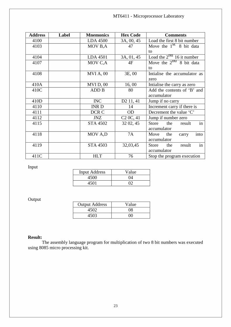
ANALOG TO DIGITAL CONVERTER Aim:
To write an assembly language program to convert analog to digital signal and to
display it in 7 segment LED display Apparatus required:
8085 microprocessor kit (0-5V) power supply
Algorithm:
Step 1 : Access the channel of ADC Step 2 : Intialise the accumulator with start of conversion signal &
output it to the ADC Step 3 : Send ‘0’ signal for ending the conversion for ADC Step 4 : Get the analog value converted to display from ADC Step 5 : The digital signal is separated into two nibbles and displayed in
hexadecimal from by calling service subroutine. Step 6 : Go to step 1
33
MT6411 - Microprocessor Laboratory
START
Load the control word necessary for generation of ALE signal to control register
Load the control word necessary to start the conversion to control register
Get the output port specified
If the 1st
LSB bit=1?
Get accumulator output in port specified
Transfer accumulator content to ‘B’
Mask all MSR & Store memory in location
Mask all 4 LSB & store memory in location
Load accumulator with 03 & with 08
Load the pair with address of MSR
Call the service subroutine
34

MT6411 - Microprocessor Laboratory
Memory Location
Hex Code Label Mnemonics Comments Op code Operand
5000 3E,10 MVI A,10 Intialise ‘a’ with 10 5002 D3,C OUT C8 Output channel through 5004 3E,18 MVI A,18 Intialise ‘A’ with 18 5006 D3, C8 OUT C8 Output channel through
8 bit port 5008 00 NOP No operation 5009 00 NOP No operation 500A 3E,10 MVI A,10 Intialise ‘A’ with 2nd
signal 500C D3,C8 OUT C8 Output channel through
8 bit port 500E 3E,01 L2 MVI A,01 Intialise ‘A’ with 2nd 5010 D3,D0 OUT D0 Output through 8 bit 5012 00 NOP 5013 00 NOP 5014 00 NOP 5015 3E,00 MVI A,00 5017 D3,D0 OUT D0 5019 DB,D8 L1 IN D8 501B E6,01 ANI 01 501D CA,19,50 JZ L1 5020 DB,C0 IN C0 Get input from 5022 47 MOV B,A B -> A 5023 E6,0F ANI 0F And of with ‘A’ 5025 32,51,51 STA 5151 Store in 5151 5028 78 MOV A,B B -> A 5029 E6,F0 ANI F0 And F0 with A 502B 0F RRC Rotate content ‘A’ 502C 0F RRC 502E 0F RRC 502F 32,50,51 STA 550 Store MSB in 5150 5032 3E,03 MVI A,03 03 -> A 5034 0E,08 MVI C,08 08 -> C 5036 21,50,51 LXI H 5150 Load ‘HL’ pair with
5150 5039 CD,05,00 CALL 0005 Call device subroutine 503C C3,0E,50 JMP 500E Jump to 500E
Result: Thus the analog to digital conversion was done microprocessor.
35

MT6411 - Microprocessor Laboratory
DECIMAL ADDITION OF TWO 8-BIT NUMBERS
Aim: To write an assembly language program for decimal addition of two8-bit numbers and sum is 8 bit.
Apparatus Required:
• 8085 Microprocessor Kit
• Power Chord
Algorithm:
Step 1: Initialise the memory location of first number in HL register pair. Step 2: Load the first number in accumulator Step 3: Increment the content of HL register pair to initialise the memory location of second data Step 4: Addition of the content of second memory location with first data Step 5: Decimal adjustment of result Step 6: Store the result in memory location 8002H
PROGRAM
Memory Machine Codes Labels Mnemonics Operands Comments
address 8100 21, 50, 80 LXI H,8050 Load the address of first
number in H-L register pair
8103 7E MOV A,M Store the first number in accumulator
8104 23 INX H Increment H-L register pair to
locate second number 8105 86 ADD M Addition of 1st and 2nd
number 8106 27 DAA Decimal Adjust
8107 32, 02, 80 STA 8002 Store result in 8002H location
810A 76 HLT Halt
RESULT : The decimal addition of two 8-bit numbers is performed using 8085 microprocessor where sum is 8-bit.
36

MT6411 - Microprocessor Laboratory
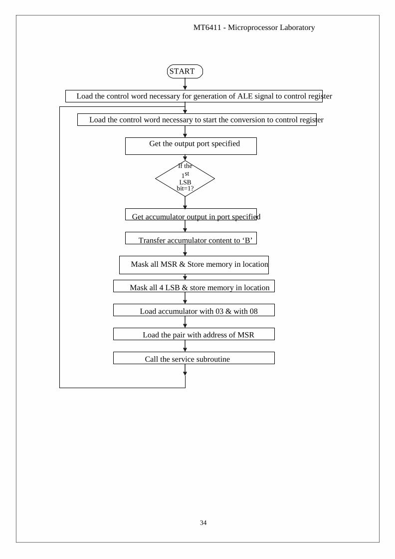
HEXADECIMAL TO DECIMAL CONVERSION: AIM:
To write an assembly language program to convert hexadecimal to decimal data using 8085-microprocessor kit. APPARATUS REQUIRED:
• 8085 Microprocessor Kit
• Power Chord ALGORITHM: Step1: Start the program. Step2: Load data from memory to accumulator and move the data 00 to D and E
registers. Step3: Compare the accumulator data with the data 64. Step4: If carry=0 jump to Step 6 else jump to Step 5. Step5: Jump to Step 10. Step6: Subtract accumulator data by 64. Step7: Increment the content of D register once. Step8: If carry=0 jump to Step 6 else jump to Step 9. Step9: Decrement the content of D register once and add data 64 with accumulator. Step10: Subtract accumulator data by 0A and Increment E register content once. Step11: If carry=0 jump to Step 10 and Decrement E register content once. Step12: Add data 64 with accumulator and move it to C register. Step13: Move E register content to accumulator. Step14: Rotate the accumulator content 4 tines by left. Step15: Add C register content with accumulator content. Step16: Store data in accumulator pair to specified memory Step17: Move D register content to accumulator Step18: Store data in accumulator pair to specified memory. Step19: End.
37
MT6411 - Microprocessor Laboratory
Memory Label
Mnemonics HEX Description
CODE
Instruc
tion Operand
4100 MVI E, 00H 1E Move data 00 to E register 4101 00 4102 MVI D, 00H 16 Move data 00 to D register 4103 00 4014 LDA 4200 3A Load data from memory to 4105 00 accumulator 4106 42 4107 CPI 64 FE Compare the accumulator data with 4108 64 the data 64 4109 JNC 410F D2 If carry=0 jump to specified memory 410A 0F 410B 41 410C JMP 4118 C3 Jump to specified memory 410D 18 410E 41 410F Loop1 SUI 64 D6 Subtract accumulator data by 64 4110 64 4111 INR D 14 Increment D register content once 4112 JNC 410F D2 If carry=0 jump to specified memory 4113 0F 4114 41 4115 DCR D 15 Decrement D register content once 4116 ADI 64 C6 Add data 64 with accumulator 4117 64 4118 Loop2 SUI 0A D6 Subtract accumulator data by 0A 4119 0A 411A INR E 1C Increment E register content once 411B JNC 4118 D2 If carry=0 jump to specified memory 411C 18
38

MT6411 - Microprocessor Laboratory
OUTPUT:
INPUT DATA: OUTPUT DATA:
4200: CE 4500: 06
4501: 02
411D 41 411E DCR E 1D Decrement E register content once `411F ADI 0A C6 Add data 64 with accumulator 4120 0A
4121 MOV C, A 4F Move accumulator content to C register
4122 MOV A, E 7B Move E register content to accumulator
4123 RLC 07
4124 RLC 07 Rotate the accumulator content 4 tines
4125 RLC 07 by left 4126 RLC 07
4127
ADD C 81
Add C register content with accumulator
content
4128 STA 4500 32 Store data in accumulator pair to 4129 00 specified memory 412A 45
412B MOV A, D 7A Move D register content to accumulator
412C STA 4501 32 Store data in accumulator pair to 412D 01 specified memory 412E 45 412F HLT 76 Halt
39

MT6411 - Microprocessor Laboratory
FLOW CHART :
Stop
START
HL 8100H
A 00
B 00H
A A +1
Decimal adjust accumulator
B B+1
D A, A B
Is A=M?
8101 A, A C 8102 A
C 00H
C C+1
Is there carry?
40

MT6411 - Microprocessor Laboratory
DECIMAL TO HEXADECIMAL
AIM:
To convert a given decimal number to hexadecimal.
ALGORITHM:
Step 1: Initialize the memory location to the data pointer. Step 2 : Increment B register. Step 3 : Increment accumulator by 1 and adjust it to decimal every time. Step 4 : Compare the given decimal number with accumulator value. Step 5 : When both matches, the equivalent hexadecimal value is in B register. Step 6 : Store the resultant in memory location.
41

MT6411 - Microprocessor Laboratory
FLOW CHART :
START
HL 4500H
A 00
B 00H
A A +1
Decimal adjust accumulator
B B+1
A B
Is A=M?
8101 A
Stop
42

MT6411 - Microprocessor Laboratory
ADDRESS OPCO
DE
LABEL MNEM ONICS
OPER AND
COMMENTS
8000 LXI H,8100 Initialize HL reg. to 8100H 8001
8002 8003 MVI A,00 Initialize A register. 8004 8005 MVI B,00 Initialize B register.. 8006 8007 LOOP INR B Increment B reg. 8008 ADI 01 Increment A reg 8009 800A DAA Decimal Adjust Accumulator 800B CMP M Compare M & A 800C JNZ LOOP If acc and given number are
not equal, then go to LOOP 800D 800E 800F MOV A,B Transfer B reg to acc. 8010 STA 8101 Store the result in a memory
location. 8011 8012 8013 HLT Stop the program
INPUT OUTPUT
ADDRESS DATA ADDRESS DATA
8100 8101
RESULT:
Thus an assembly language program to convert hexadecimal to decimal and decimal to hexadecimal data’s was written and executed using 8085-microprocessor kit.
43

MT6411 - Microprocessor Laboratory
STEPPER MOTOR CONTROLLER
AIM:
To write a program fro inter facing stepper motor and to run the motor in different directions and in different speeds. ALGORITHM: Step1: Start the program. Step2: Load HL register pair with memory address at look up. Step3: Move the contents of HL pair to accumulator. Step4: Out the contents of accumulator to run the motor. Step5: Decrease b register. If register content is not zero then rotate the motor
continuously. Step6: If zero then move to the Seginning of the program. Step7: Stop the process. THEORY: STEPPER MOTOR:
A motor in which the rotor is able to assume only discrete stationary angular position is a Stepper Motor. The rotary motion in a stepper motor is a stepwise manner from one equilibrium position to another. CONSTRUCTIONAL FEATURES: A stepper motor could be either of the reluctance type or of the permanent magnet type (PM). A PM stepper consists of multiphase stator and two part permanent magnet rotor. The VR stepper motor has unmagnetised rotor. PM stepper motor is the most commonly used type. The basic two phase stepper motor consists of two pairs of stator poles. Each of the four poles has its own winding. The excitation of any winding generates a north pole (N), a south pole (S) gets induced at the diametrically opposite side.
44

MT6411 - Microprocessor Laboratory
As shown in the figure the four pole structure is continuous with the stator
frame and the magnetic field passes through the cylindrical stator annular ring. The
rotor magnetic system has two end faces. The left face is permanently magnetized as
South Pole and their right face as North Pole. The South Pole structure and the North
Pole structure posses similar pole faces. The north pole structure is twisted with
respect to the south pole structure by one pole pitch.
Stepper Motor Cross-sectional View
45

In an arrangement where four stator poles and three poles of rotor poles, there exists 12 possible positions in which a south pole of the rotor can lock with a north pole of the stator. From this it can be rotated that the step size is
360o =
Ns*Nr
where, Ns is the number of stator pole pairs Nr is the
number of pairs rotor pole
Generally step size of the stepper motor depends upon NR. These stable positions can be
attained by simply energizing the winding on any one of the stator poles with a DC. There are
three different schemes available for ‘stepping’ a stepper motor. They are,
a) Wave Scheme
b) 2-Phase scheme
c) Half stepping or mixed scheme 2-PHASE SCHEME:
In this scheme any two adjacent stator windings are energized. There are two magnetic
fields active in quadrature and none of the rotor pole faces can in direct alignment with the
stator poles. A partial but symmetric alignment of the rotor poles is of course possible.
Typical equilibrium conditions of the rotor when the windings on two successive stator
poles are excited are illustrated. In Step (a) A1 and B1 are energized. The pole-face S1 tries to
align itself with the axis of A1 (N) and the pole-face S2 with B1 (N). The North Pole N3 of the
rotor finds itself in neutral zone between A1 (N) and B1 (N). S1 and S2 of the rotor position
themselves symmetrically with respect to the two stator north pole.
46

Next when B1 and A2 are energized S2 tends to align with B1 (N) and S3 with A2 (N)
of course. Again under equilibrium conditions only partial alignment is possible and N1 finds
itself in the neutral region midway between B1 (N) and A2 (N) [Step (b)]. In Step (c), A2(N)
and B2(N), respectively, with N2 in the neutral zone. Step (d) illustrates the case when A1 and
B2 are ON.
The step angle is 30ْ as in the two phase’s scheme. However the rotor is offset by 15ْ in
the two phase’s scheme with respect to the wave scheme. A total of 12 steps are required to
move the rotor by 360ْ (mechanical) Two Phases drives produce more torque than the wave
drives.
LOOK UP TABLE
Anticlockwise Clockwise
Step A1 A2 B1 B2 A1 A2 B1 B2
1 1 0 0 1 1 0 1 0
2 0 1 0 1 0 1 1 0
3 0 1 1 0 0 1 0 1
4 1 0 1 0 1 0 0 1
Memory Label Mnemonics HEX Description
CODE
Instruc
tion Operand
4100 START: LXI H, LOOK UP 21 Load HL pair with memory address
4101 1A at Look Up 4102 41 4103 MVI B,04 06 Move immediate the given data 4014 04 to B register 4105 REPT: MOV A,M 7E Move content of memory to Acc. 4106 MOV [2000], AX 03 Out the content of Accumulator 4107 C0 to C0 port address 4108 LXI D, 0303H 11 Load the data 0303H to D register 4109 03 410A 03 410B DELAY: NOP 00 Perform No operation
47

410C DCX D 1B Decrement address of DE pair once 410D MOV A,E 7B Move E register content to Acc. 410E ORA D B2 Perform OR operation With Acc. 410F JNZ 410B C2 Jump on no zero to the 4110 0B instruction at specified memory
4111 41 Address
4112 INX H 23 Increment HL pair address once
4113 DCR B 05 Decrement B register content once
4114 JNZ C2 Jump on no zero to the
4115 05 instruction at specified memory
4116 41 Address
4117 JMP START C3 Jump to the instruction at
4118 00 specified memory
4119 41
411A LOOK UP 09 Data will be stored in the location
05
06
04 RESULT:
Thus the stepper motor is rotated by varying the speed using COUNT operation and
its direction is also changed using program written and executed using 8085 micro processor kit.
48