Chemiresistive Gas Sensor Array based on Metal Oxide … · 2019-04-10 · Healthcare and...
11
Healthcare and biomarkers Gas sensing mechanism 2×4 sensor array & Temperature optimization 1750 1800 1900 1950 1990 2009 2020 1850 Healthcare 1.0 (Infectious disease care) Healthcare 2.0 (Disease care) Healthcare 3.0 (Preventive care) Mortality per million 7,000 6,000 5,000 4,000 3,000 2,000 1,000 0 90 80 70 60 50 40 30 0 20 10 Age Disease Associated volatile biomarker (Detection limit) Health Patient Asthma NO 2 (20~30 ppb) NO 2 (< 100 ppb) Diabetes CH 3 COCH 3 (> 0.9 ppm) CH 3 COCH 3 (< 1.8 ppm) Oral inflammation H 2 S(> 100 ppb) H 2 S(< 1 ppm) Electron beam evaporator (off-axis mode) Source 2x4 array sensor Back heater Chip carrier Heater wire Au Pt Pd Catalyst decoration (on-axis mode) Metal oxide nanocolumns (In 2 O 3 , WO 3 ) Pt Pt SiO 2 /Si In 2 O 3 WO 3 Sensing material (a) (b) (c) Resistance (Ω) Gas in (reducing gas) Times (s) O – O – O – O – O – O – O – O – O – O – O – O – O – O – O – O – O – O – O – O – O – O – O – E F E C qV s Electron transfer Adsorbed oxygen (over 150℃) Depletion layer Grain Double Schottky barriers Nanocolumn Nanotube ① High sensitivity ② High selectivity Low-power consumption Small size sensor Nanostructures & Catalyst Heater Sensing material Sensor array & Data patterning ③ CH 3 COCH 3 NO 2 H 2 S C 6 H 7 • • • Gas sensor array based on semiconductors Fabrication procedures 500 ppb 100 200 300 400 on off CH 3 COCH 3 Pd_In 2 O 3 Detection limit : 8.28 ppb 500 ppb 100 200 300 400 on off H 2 S Au_WO 3 Detection limit : 2.47 ppb 50 ppb 10 20 30 40 on off NO 2 Au_In2O3 Detection limit : 20 ppb NO 2 at 150 o C CH 3 COCH 3 at 300 o C H 2 S at 250 o C (a) (b) (c) (d) (e) (f) NO 2 CH 3 COCH 3 H 2 S 150℃ 300℃ 250℃ Au_In 2 O 3 Pd_In 2 O 3 Au_WO 3 NO 2 1 ppm CH 3 COCH 3 10 ppm Bare In 2 O 3 Au_In 2 O 3 Pt_In 2 O 3 Pd_In 2 O 3 Bare W O 3 Au_WO 3 Pt_WO 3 Pd_WO 3 H 2 S 1 ppm (a) (b) (c) Heater WO 3 Au_WO 3 Pt_WO 3 Pd_WO 3 Heater In 2 O 3 Au_In 2 O 3 Pt_In 2 O 3 Pd_In 2 O 3 300 o C 300 o C Bare In 2 O 3 Au_In 2 O 3 Pt_In 2 O 3 Pd_In 2 O 3 Bare WO 3 Au_WO 3 Pt_WO 3 Pd_WO 3 (a) (b) (c) Detection limits in high humidity (RH 80%) • Healthcare, which has been waiting for the patient to be sick, will be replaced by personalized, predictive, preventive and participatory (P4) medicine. • Disease diagnosis based on exhaled breath is inexpensive and noninvasive method to characterize abnormalities linked to medical conditions. • Semiconducting gas sensors have been much attention within sensor society cue to their high sensitivity, small size and cost effectiveness and easy to integration with other circuits. • Sensor arrays enhance the selectivity via data patterning and reduce the power- consumption which is an important parameter for battery-loaded wireless sensors. • Conventional gas sensing mechanisms could be explained by oxygen adsorption / desorption and double Schottky barriers . • Glancing angle deposition (GLAD) based on e-beam evaporator was used to fabricate 2x4 sensor array. • Our results show extremely low detection limits to distinguish the biomarkers from exhaled breath. • Temperature optimization was carried out using micro-heater as a function of biomarkers Chemiresistive Gas Sensor Array based on Metal Oxide Semiconductor for Exhaled Breath
Transcript of Chemiresistive Gas Sensor Array based on Metal Oxide … · 2019-04-10 · Healthcare and...

Healthcare and biomarkers
Gas sensing mechanism
2×4 sensor array & Temperature optimization
1750 1800 1900 1950 1990 2009 20201850
Healthcare 1.0(Infectious disease care)
Healthcare 2.0(Disease care)
Healthcare 3.0(Preventive care)
Mor
talit
y pe
r m
illio
n
7,000
6,000
5,000
4,000
3,000
2,000
1,000
0
90807060504030
0
2010
Age
DiseaseAssociated volatile biomarker (Detection limit)
Health PatientAsthma NO2 (20~30 ppb) NO2 (< 100 ppb)
Diabetes CH3COCH3 (> 0.9 ppm) CH3COCH3 (< 1.8 ppm)
Oral inflammation H2S (> 100 ppb) H2S (< 1 ppm)
Electron beam evaporator(off-axis mode)
Source2x4 array sensor
Back heater
Chip carrier
Heater wire
AuPtPd
Catalyst decoration(on-axis mode)
Metal oxide nanocolumns(In2O3, WO3)
PtPtSiO2/Si
In2O3 WO3Sensing material(a) (b)
(c)
Res
ista
nce
(Ω) Gas in
(reducing gas)
Times (s)
O–O–
O–O–O–O–
O–O–
O–
O–
O–
O–
O–
O–
O–
O–O–O–O–O– O–
O–O–
EF
ECqVs
Electron transfer
Adsorbed oxygen (over 150)
Depletion layerGrain
Double Schottky barriers
Nanocolumn
Nanotube
① High sensitivity ② High selectivity Low-power consumption
Small size sensor Nanostructures & Catalyst
Heater
Sensing material
Sensor array & Data patterning
③
CH3COCH3NO2H2SC6H7
••
•
Gas sensor array based on semiconductors
Fabrication procedures
500 ppb100 200 300 400onoff
CH3COCH3
Pd_In2O3Detection limit : 8.28 ppb
500 ppb100 200 300 400onoff
H2S
Au_WO3Detection limit : 2.47 ppb
50 ppb10 20 30 40onoff
NO2
Au_In2O3Detection limit : 20 ppb
NO2 at 150 oC CH3COCH3 at 300 oC H2S at 250 oC
(a) (b) (c)
(d) (e) (f)
NO2 CH3COCH3 H2S
150 300 250
Au_In2O3 Pd_In2O3 Au_WO3NO2 1 ppm CH3COCH3 10 ppmBare In2O3
Au_In2O3
Pt_In2O3
Pd_In2O3
Bare WO3
Au_WO3
Pt_WO3
Pd_WO3
H2S 1 ppm
(a) (b) (c)
HeaterWO3
Au_WO3
Pt_WO3
Pd_WO3
Heater
In2O3
Au_In2O3
Pt_In2O3
Pd_In2O3
300 oC
300 oC
Bare In2O3
Au_In2O3
Pt_In2O3
Pd_In2O3
Bare WO3
Au_WO3
Pt_WO3
Pd_WO3
(a) (b) (c) Detection limits in high humidity (RH 80%)
• Healthcare, which has been waiting for the patient to be sick, will be replaced by personalized, predictive, preventive and participatory (P4) medicine.
• Disease diagnosis based on exhaled breath is inexpensive and noninvasive method to characterize abnormalities linked to medical conditions.
• Semiconducting gas sensors have been much attention within sensor society cue to their high sensitivity, small size and cost effectiveness and easy to integration with other circuits.
• Sensor arrays enhance the selectivity via data patterning and reduce the power-consumption which is an important parameter for battery-loaded wireless sensors.
• Conventional gas sensing mechanisms could be explained by oxygen adsorption / desorption and double Schottky barriers.
• Glancing angle deposition (GLAD) based on e-beam evaporator was used to fabricate 2x4 sensor array.
• Our results show extremely low detection limits to distinguish the biomarkers from exhaled breath.
• Temperature optimization was carried out using micro-heater as a function of biomarkers
Chemiresistive Gas Sensor Array based on Metal Oxide Semiconductor for Exhaled Breath
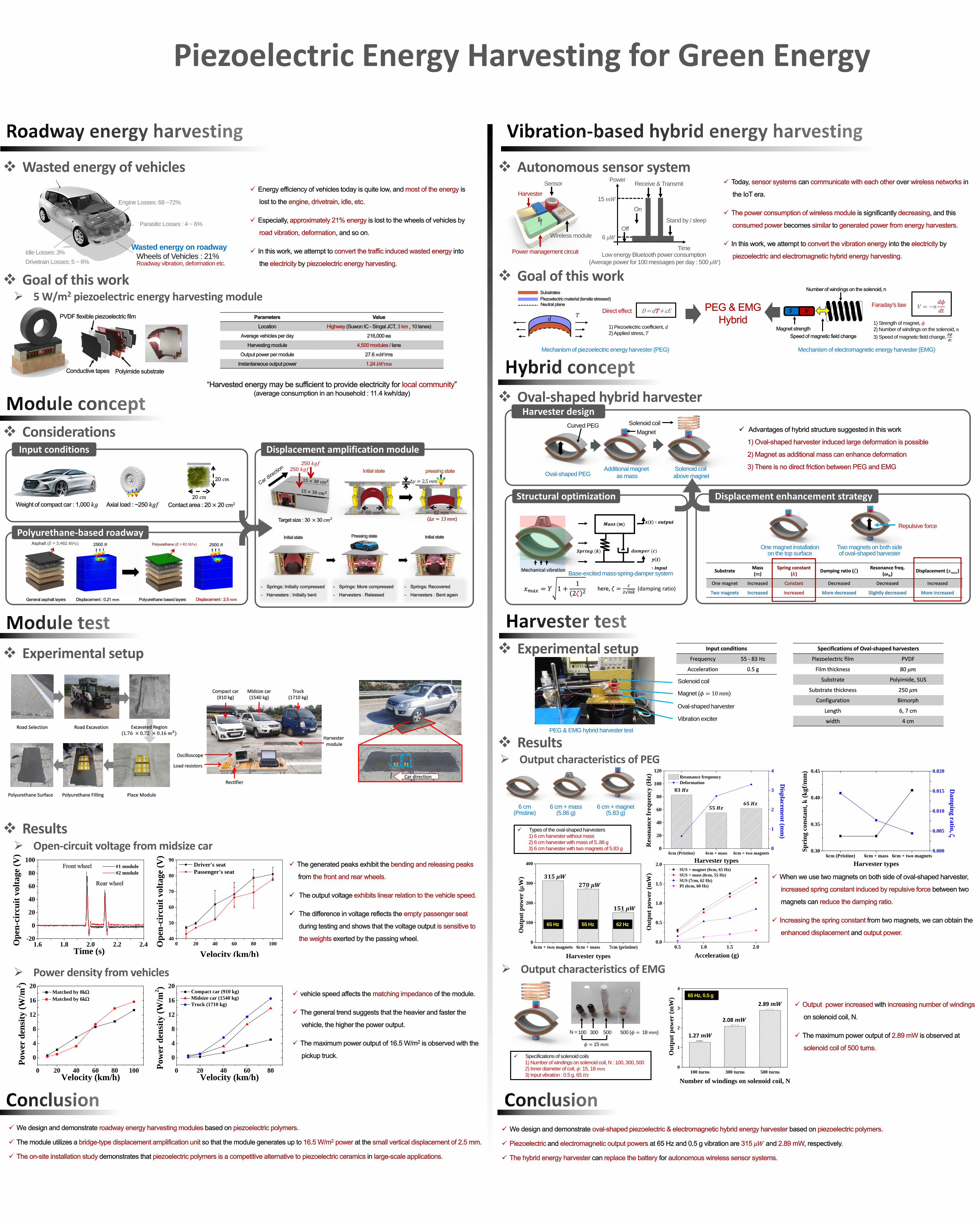
One magnet installation on the top surface
Two magnets on both side of oval-shaped harvester
Repulsive force
𝑺𝑺𝑺𝑺𝑺𝑺𝑺𝑺𝑺𝑺𝑺𝑺 (𝒌𝒌) 𝒅𝒅𝒅𝒅𝒅𝒅𝑺𝑺𝒅𝒅𝑺𝑺 (𝒄𝒄)
Base-excited mass-spring-damper system
Piezoelectric Energy Harvesting for Green Energy
Goal of this work
15 𝑚𝑚𝑊𝑊
6 𝜇𝜇𝑊𝑊
Receive & Transmit
On
Stand by / sleepOff
Power
TimeLow energy Bluetooth power consumption
(Average power for 100 messages per day : 500 𝜇𝜇𝑊𝑊)
Sensor
Wireless module
Harvester
Power management circuit
Autonomous sensor system Wasted energy of vehicles
Parasitic Losses : 4 ~ 6%
Engine Losses: 68 ~72%
Idle Losses: 3%Drivetrain Losses: 5 ~ 6%
Wasted energy on roadwayWheels of Vehicles : 21%Roadway vibration, deformation etc.
Goal of this work 5 W/m2 piezoelectric energy harvesting module
Oval-shaped hybrid harvester
Polyurethane-based roadway
Displacement amplification module
250 𝑘𝑘𝑘𝑘𝑘𝑘250 𝑘𝑘𝑘𝑘𝑘𝑘
Experimental setup
Results
1.6 1.8 2.0 2.2 2.4-20
0
20
40
60
80
100
Ope
n-ci
rcui
t vol
tage
(V)
Time (s)
#1 module #2 module
0 20 40 60 80 100
0
4
8
12
16
20
Pow
er d
ensi
ty (W
/m2 )
Velocity (km/h)
Matched by 8kΩ Matched by 6kΩ
0 20 40 60 80
0
4
8
12
16
20
Pow
er d
ensi
ty ( W
/m2 )
Velocity (km/h)
Compact car (910 kg) Midsize car (1540 kg) Truck (1710 kg)
0 20 40 60 80 10040
50
60
70
80
90
Ope
n-ci
rcui
t vol
tage
(V)
Velocity (km/h)
Driver's seat Passenger's seat
Open-circuit voltage from midsize car
Power density from vehicles
Δ𝑦𝑦
D = dT + εE
1) Piezoelectric coefficient, 𝑑𝑑2) Applied stress, 𝑇𝑇
𝑇𝑇𝑑𝑑Direct effect
Faraday’s law
1) Strength of magnet, 𝜙𝜙2) Number of windings on the solenoid, 𝑛𝑛3) Speed of magnetic field change, 𝑑𝑑𝜙𝜙
𝑑𝑑𝑑𝑑
𝑉𝑉 = −𝑛𝑛𝑑𝑑𝜙𝜙𝑑𝑑𝑑𝑑𝑵𝑵𝑺𝑺
6cm (Pristine) 6cm + mass 6cm + two magnets0.30
0.35
0.40
0.45
Harvester types
Spri
ng c
onst
ant,
k (k
gf/m
m)
0.000
0.005
0.010
0.015
0.020
Dam
ping ratio, ζ
6cm (Pristine) 6cm + mass 6cm + two magnets0
20
40
60
80
100
120 Resonance frequency Deformation
Harvester types
Res
onan
ce fr
eque
ncy
(Hz)
0
1
2
3
4
Displacem
ent (mm
)
𝟖𝟖𝟖𝟖 𝑯𝑯𝑯𝑯
𝟓𝟓𝟓𝟓 𝑯𝑯𝑯𝑯𝟔𝟔𝟓𝟓 𝑯𝑯𝑯𝑯
314270
151
6cm + two magnets 6cm + mass 7cm (pristine)0
100
200
300
400
Out
put p
ower
(µW
)
Harvester types
65 Hz 55 Hz 62 Hz
𝟖𝟖𝟑𝟑𝟓𝟓 𝝁𝝁𝝁𝝁𝟐𝟐𝟐𝟐𝟐𝟐 𝝁𝝁𝝁𝝁
𝟑𝟑𝟓𝟓𝟑𝟑 𝝁𝝁𝝁𝝁
0.5 1.0 1.5 2.00.0
0.5
1.0
1.5
2.0
Out
put p
ower
(mW
)
Acceleration (g)
SUS + magnet (6cm, 65 Hz) SUS + mass (6cm, 55 Hz) SUS (7cm, 62 Hz) PI (6cm, 60 Hz)
Input conditions
Oval-shaped PEGAdditional magnet
as massSolenoid coil above magnet
Curved PEGMagnet
Solenoid coil
Considerations
Experimental setup
Results Output characteristics of PEG
Output characteristics of EMG
Solenoid coil
Oval-shaped harvester
Vibration exciter
Magnet (𝜙𝜙 = 10𝑚𝑚𝑚𝑚)
PEG & EMG hybrid harvester test
N = 100 300 500 500 (𝜙𝜙 = 18 𝑚𝑚𝑚𝑚)
𝜙𝜙 = 15 𝑚𝑚𝑚𝑚
6 cm(Pristine)
6 cm + mass(5.86 g)
6 cm + magnet(5.83 g)
Types of the oval-shaped harvesters1) 6 cm harvester without mass2) 6 cm harvester with mass of 5..86 g3) 6 cm harvester with two magnets of 5.83 g
(damping ratio)
Specifications of solenoid coils1) Number of windings on solenoid coil, N : 100, 300, 5002) Inner diameter of coil, 𝜙𝜙: 15, 18 𝑚𝑚𝑚𝑚3) Input vibration : 0.5 g, 65 𝐻𝐻𝐻𝐻
Harvester design
Structural optimization Displacement enhancement strategy
Mechanism of piezoelectric energy harvester (PEG) Mechanism of electromagnetic energy harvester (EMG)
1.27
2.08
2.89
100 turns 300 turns 500 turns0
1
2
3
4
Out
put p
ower
(mW
)
Number of windings on solenoid coil, N
65 Hz, 0.5 g
1.27 𝒅𝒅𝝁𝝁
2.08 𝒅𝒅𝝁𝝁
2.89 𝒅𝒅𝝁𝝁

Electrochemically driven Mechanical Energy Harvesting
Efficient mechanical energy harvesters convert wasted motions and vibrations into useful electricity.
Thermodynamic working principle
The harvester possesses unique benefits at low-frequency motions
We design a ‘mechanically rechargeable battery’ as an energy harvester.
Device fabrication Current generationElectrode and silicon deposition on PI:
Shaping and electrochemical lithiation:
Device assembly with PDMS surfaces:
Bending and bending the device generates potential differences:
Generated current peaks have 3 second half-life:
Repeatedly bending for 1500 times generates continuous current output, with minimal damages observed:
The device accommodates different mechanical frequency inputs:
Applying stress to electrodes changes the electrochemistry:
h
x
y -z
Δ𝜇𝜇bottom−top = ΩLiΔ𝜎𝜎hydro
= ΩLiE
1 − 𝜈𝜈2h3𝑅𝑅
ΩLi =𝜕𝜕𝑉𝑉𝜕𝜕𝑁𝑁𝐿𝐿𝐿𝐿 𝑃𝑃,𝑇𝑇,𝑁𝑁𝑖𝑖≠Li
where
The power output may be described as the following:2 2
Li one-sideLi Li 2 2
2 21 2 1 23 (1 ) 3 (1 )
LiN E V Eh hNR R
ν νµν ν
Ω − − ∆ ∆ = = − −
Input frequency of f = 0.07 Hz, 100 cycles
Input frequency of f = 0.20 Hz, 100 cycles
We may design an energy harvester optimized for specific frequency motion:

0 1000 2000 3000 40000
50
100
150
200
Resis
tanc
e [MΩ
]
Time [s]
5 ppm NO2
S = 121%
0 10 20 30 400
5
10
15
20
Drain voltage [V]
Drai
n cu
rrent
[µA]
VGS-Vth= -30 VVGS-Vth= -20 VVGS-Vth= -10 VVGS-Vth= 0 V
120 160 200 240 280 320 360 400
SnS B3g
SnS Ag
Tg = 240oCTg = 210oCTg = 180oC
Raman shift [cm-1]
Inte
nsity
[arb
. uni
t]
Tg = 150oCTg = 120oCTg = 90oC
SnS2
SnS Ag
<Gas sensor>
< Layer structure> <Raman spectra>
< Thin film transistor>
2-D Materials : The Next-generation Channel Layers
Why 2-D?
MoS2
A injection purge B injection purgeadsorption removal of excess A reaction removal of excess B
and byproducts
<Future electronic devices> <2D layered chalcogenides>
Challenges Large area display Flexible and soft electronics High electronic mobility Low power consumption
Advantages of 2-D materials High electronic mobility Flexible Open band gap high on/off ratio
<MoS2> <SnS>
1. thickness controllability2. Good uniformity 3. Excellent stepcoverage
<ALD process>
1
2
3
4
Film
s th
ickn
ess
Cycle number
<Advantages of ALD>
n-SnS2
2 nm
epoxy
SiO2
d(002)=0.63 nm
340 360 380 400 420 440 460
Inte
nsity
[a.u
]
Raman shift [cm-1]
60s 30s 10s 5s
E2g
A1g
< Layer structure> <Raman spectra>
< Wafer growth>
10 20 30 40 50
annealing in H2S
annealing in Ar
Inte
nsity
[arb
. uni
t]
2θ [degree]
as-dep.
(002)
<Crystallinity> < Thin film transistor>
0.1 V1 V10 V
VDS
Mob
ility
[cm
2 /V
s]
16 V12 V8 V4 V0 V
VGS
SiO2
Al2O3
d=0.59 nm
10 nm
< Layer structure>
SnS2 A1g5 min10 min 30 min60 min
<Raman spectra>
Why ALD?
p-SnS
SnO or SnO2 SnSx SnS2
Sulfurization H2S plasma
<Sulfurization method> <Device fabrication>
Etching & Lift-off method
Thin film transistor
Gas sensor

Research on Next-generation Dynamic Random Access Memory Capacitor
Research trend of DRAM capacitor
Influence of reduced Al-doping concentration on electrical properties of TiO2
Removal of interfacial layers at the interface between polysilicon and dielectric material in SIS or MIS capacitors is necessary for sub 20nm scaled DRAM. So, capacitor structure has been changed to a metal-insulator-metal (MIM) structure recently.
The technology road map for memory devices states that tox less than 0.3nm is necessary for the DRAMs with a design rule of 1Xnm. The ever-shrinking dimensions of DRAM cells with the increasing packing density have made the capacitor size increasingly smaller and currently-used ZrO2 dielectric will not be able to maintain necessary capacitance. We choose rutile TiO2and cubic BeO as the promising dielectric layers for DRAM capacitor.
0 100 200 300 400 500 600-100
-50
0
50SnO2 + 2H2 = SnO + H2O
∆Gr [k
cal/m
ol]
Temperature [oC]
RuO2 + 2H2 = Ru + 2H2O
SnO2 + 2H2 = Sn + 2H2O
-0.50 -0.25 0.00 0.25 0.500
20
40
60
80
100
Diel
ectri
c co
nsta
nt
Applied voltage [V]
Pristine Ann. in H2
Ta-SnO2
RuO2
-2 -1 0 1 210-10
10-8
10-6
10-4
10-2
100
close: Pristineopen: Ann. in H2
Curre
nt d
ensit
y [A
/cm
2 ]
Electric field [MV/cm]
Red: Ta-SnO2
Blue: RuO2
• Regardless of heat treatment, crystal structure and electrical properties of TiO2 do not change on the Ta-SnO2• On the other hand, deterioration by heat treatment was observed on RuO2• The work function of RuO2 decrease from 5.2eV to 4.7eV, while work function of Ta-SnO2 does not change
Ta doped SnO2 as a DRAM capacitor electrode
C. J. Cho et al., J. Mater. Chem. C, 2017,5, 9405-9411
• The competitive adsorption method(co-feeding) significantly reduces TMA chemisorption• In the case of double doping layer, leakage current is effectively suppressed as expectation• tox of the films is negligibly increased
Al doping into rutile phase TiO2 Ideal Dielectric : Higher k & Larger band gap O3
Ru RuO2
TiO2
@ 250oCby ALD
• In order to obtain Rutile TiO2 growth at low temperature, RuO2 interface was induced by O3 oxidation
• Rutile TiO2 has small band gap and n-type nature. Al doping enhance leakage current properties by elevating Schottky barrier height.
• Al doped TiO2 show lower leakage current with same equivalent oxide thickness.
Wurtzite BeO Rocksalt BeO
• Band gap : 10.6eV• Dielectric Constant : 7~8
• Band gap : 10.1eV• Dielectric Constant : 274
• The phase transformation to rocksaltBeO requires really high pressure (~100GPa)
Sahariah and Ghosh, J. App. Phys. (2010) Park et al., Phys. Rev. B (1999)
S. K. Kim et al., Adv. Mater., 2008, 20, 1429-1435
W. J. Jeon et al., ACS Appl. Mater. Interfaces, 2014, 6 (10)
35 40 45 50 55 60 65 70
wurtzite (002)
wurtzite (100)
MgO:BeO=68:32
MgO:BeO=81:19
Inte
nsity
[arb
. uni
t]
2theta [degree]
MgO:BeO=100:0
rocksalt (220)
rocksalt (200)
MgO:BeO=62:38
MgO:BeO=54:46
MgO:BeO=48:52
MgO:BeO=41:59
MgO:BeO=33:67
MgO:BeO=24:76
MgO:BeO=17:83
MgO:BeO=0:100
Stabilization of cubic BeO : BexMg1-xO
Mg increase
Cubic Structure
• Rocksalt-structured BexMg1-xO films have an enhanced dielectric constant (~20)

Thermoelectric Power Generating Systemfor Wearable Devices
Industrial and technological mega-trend
Digital Single Function
Multi-Function,Unconnected
Multi-Function,Connected
Always connected,Smart&Wearable
Battery-freeLow power consumption
Wearable Tech Market to Reach $26B by 2025Potential Role of IoT Drive E- Harvesters
Source; 2014 , IDTechEx
Thermoelectric46%
“The energy harvesting market by component reaching $596 million in 2018, up from $163 million in 2014”
Thermal energy
Electrical energy
Module structure Commercial module
Lairdtech co. IntRMT Int.
Wireless Body-Area Network
Wearable energy havesting from human body
Thermoelectric power generation for wearable devices
Bi2Te3-based material
κσTSZT
2
=
S : Seebeck coefficient σ : Electrical conductivity K : Thermal conductivityT : Temperature
Figu
re-o
f-mer
it, Z
T
Materials synthesis strategies Device design & fabrication
Electron creation mechanism Powder-free hot extrusion Wearable thermoelectric device
A. Nanostructuring B. Texturing
Randomly-oriented Textured
Low mobility High mobility
a-axisc-axis
High density device fabrication ( > 50 pairs)
Proto-type wearble device
FEM modeling (Structure optimization)
Pole figure analysis
Fiber texturing
High reproducibility
J-.H. Bark et al. JMCC (2015)NPG Asia Mater. (2010)
c
a

Epitaxial Multifunctional Oxide Thin Film
Non-volatile control of 2DEG conductivity at LAO/STO interface using ferroelectric polarization switching of epitaxial PZT overlayer.
Electrical conductance is governed by depletion/accumulation of 2DEG as well as conducting filament formation in TaOx layer.
Defect control of oxide layer: Re-RAMOxide interface control: 2DEG
Anion control of epitaxial thin film
Epitaxial SnON thin film exhibited highly improved mechanical hardness due to the compact and dense crystal structure of cubic SnONas a high-pressure phase.
Phase control of thin film with buffer layers
VOx thin film deposited on STO buffer showed pure VO2(A) phase and had high TCR & low resistivity values simultaneously.
TCR: -3.40%/KResistivity: ~0.1 Ω∙cm at RT
TCR: -3.19 %/KResistivity: ~5 Ω∙cm at RTVO2(A)
110
VO2(A)220
V3O7-111
V2O5001
VO2(A)110
Si Substrate
Si Substrate
Thin film deposition technique Thin film analysis methods
Crystalline types of solid Multifunctional oxidePerovskite (ABO3)
ABO
• Ferroelectric, Piezoelectric• Multiferroic• Dielectric• (Anti) ferromagnetic• Metallic, Semiconductor,
Insulator• Superconductor• Colossal Magnetoresistance• Giant Piezoelectric, etc.
Couplings
Epitaxial oxide thin film
• Scientific interests : What is the intrinsic property?• Technological interests : How to enhance the properties?
1. Strain engineering 2. Domain engineering3. Defect engineering4. Interface engineering
Single-crystalline Poly-crystalline
INTRINSIC property from unit cell (elements and symmetry)
+ EXTRINSIC property from grain / domain boundaries
Amorphous
Lack of long-range order
Pulsed Laser Deposition Sputtering
XRD
TEM
AFM
Hall measurement
• Crystallographic structure• Nanostructure analysis
• Morphology of thin film• Carrier concentration• Hall mobility
Vacuum chamber
Substrate
GunPlasma
RFAr+O2

-40 -20 0 20 40-40
-20
0
20
40
Pola
rizat
ion
(µC/
cm2 )
Drive Voltage (V)
Epitaxial Piezoelectric Thin Film on Si forPiezoelectric Micromachined Ultrasonic Transducer
Orientation control by template
: Pt (top electrode): PMN-PZT
: Silicon: SiO2
AC~
relec
rwavehwave
hSi
hpiezo
Acoustic waveguide
: SrRuO3 (bottom electrode)
pMUT single cell 4th generation relaxor ferroelectrics
Template schematic
Optimizing piezoelectric propertyEpitaxial thin film deposition
20 50
Si 0
04SR
O 2
20
SRO
110
CeO
200
2YS
Z 00
2
30 6040 70 80
(110) SRO/CeO2/YSZ/Si
2 theta(°)
Si 0
04
LSM
O 0
02
LSM
O 0
01
CeO
200
2YS
Z 00
2
LSM
O 0
03
2 theta(°)
20 5030 6040 70 80
(001) LSMO/CeO2/YSZ/Si
Structural characterization
Heater
Off-axis Sputtering
Particle with High Energy
Particle with Low Energy
Substrate
Multi-gun off-axis sputtering
• Defect dipole• Point defect
• Domain structure• Domain walls
• Thermal strain• Lattice strain• Strain gradient
• Substrate Clamping
Thin film
Substrate
Composition (% of ferroelectric)
Extrinsic effect of thin Film Strain effect Orientation dependence
GADDS analysis
20 30 40 50 60 70100
101
102
103
104
105
106
107
Inte
nsity
(cps
)
2θ
YSZ
(002
)
YSZ
(004
)
Si (004)
CeO
2(0
02)
CeO
2(0
04)
LSM
O (0
01)
LSM
O (0
02)
LSM
O (0
03)
PMN
-PZT
(001
)
PMN
-PZT
(002
)
XRD P – E curve
Template design for epitaxial piezoelectric film
Single CrystalPZN-4.5%PT
(001)Single CrystalPZN-8%PT
(001)
Ceramics, PZT-5H
Ceramics, PMN-PTCeramics, PZT-8
0.8
0.6
0.4
0.2
0.020 40 60 800
Electric Field (kV/cm)
Stra
in (%
) Single CrystalPZN (001)
1st generation· High d33, k33
· Low TC, TRT, EC, Qm
2nd generation· High TC, TRT, EC
· Low Qm
3rd generation· High d33, k33, Qm
· Low TC, TRT, EC
4th generation· High d33, k33, TC, TRT, EC, Qm
Buffer Layers
Si (001)
SiO2
Si (001)
Piezoelectric Layer
Oxide Electrode
pMUT array
Epitaxial 4th generation relaxor ferroelectrics are chosen for its high d33, TC and TRT values.For pMUT, epitaxial piezoelectric filmshould be deposited on Si. Thus, proper buffer layers are required.
Different lattice constant of oxide films makedifferent orientation on CeO2/YSZ template
Piezoelectric property can be enhanced by extrinsic factors, strain and orientation of thin film.
Epitaxially grown piezoelectric layer on template shows hysteresis loop.
4 X 4 array N X N array

Multi-environmental Energy Harvesting Based on New Energy Conversion Mechanisms
Piezoluminescence stress/strain sensor
Mechanical Energy Light Emission Photobiomodulation Therapy
<In-Vivo Piezo-luminescence driven by Ultrasonic>
Dual phase broadband energy harvester: vibration and magnetic field
30 40 50 60 70 80 90 1000
1020304050607080
Frequency (Hz)
Out
put v
olta
ge (V
)
30 40 50 60 70 80 90 10005
1015202530354045 Beam #1
Beam #2 Beam #3 Beam #4 Beam #5
Frequency (Hz)
Out
put v
olta
ge (V
)
500 μT magnetic field
30 40 50 60 70 80 90 10005
101520253035404550
Beam 1 Beam 2 Beam 3 Beam 4 Beam 5
Frequency (Hz)
Out
put v
olta
ge (V
)
30 40 50 60 70 80 90 1000
102030405060708090
Frequency (Hz)
Out
put v
olta
ge (V
)
Broadband
Electric kettleOscilloscope
E harvester
Energy harvester
Rectifying circuits Oscilloscope
Thermo-magneto-electric generator for low-grade thermal energy Operation principle of thermo-magneto-electric generator (TMEG)
Magnetic Piezoelectric
Heating
Cooling
CurieTemperature
(Tc)
Hard magnet
Soft magnet Piezoelectric
Hot side
Cold side
Hot side (70oC)
Hard magnet (Nd)
Soft magnet (Gd)Cold side (-10oC)
Cantilever (PVDF)
Thermo-Magneto-Electric Generator (TMEG)
2 cm
TMEG
Heat sink module
Applications Heat sink for improving the power output of solar photovoltaic cells
Incorporation of photovoltaic harvesting systems in airborne platforms
Army LEMV Boeing Solar EagleSolar cell heat sink
Exploit thermally induced second order phase transition of soft magnet
Power generating from periodic oscillation of piezoelectric materials on spring
50 100 150 200 250 300 350
0
10
20
30
40
50
60
70 H=500 Oe
Mag
netiz
atio
n (e
mu/
g)
Temperature (K)
-20 -10 0 10 20
-120
-90
-60
-30
0
30
60
90
120
50K 100K 200K 250K 300K 350K
Mag
netiz
atio
n (e
mu/
g)
Magnetic field (kOe) 0.00 0.25 0.50 0.75 1.00-2
0
2
4
Volta
ge (V
)
Time (sec)
Hea
ting
Coo
ling
Heating
Cooling
Inside desktop
Hard magnet on CPU
Gadolinium (Gd)
TMEG operation from CPU heat
LED operation
Ferromagnetic State Paramagnetic State
Thermal E Mechanical E Electrical E
Dual phase energy harvester Applications Vibration condition Magnetic field condition
1 g acceleration E harvesting from a power cord E harvesting from a car Engine
<Stretching>
<Releasing>
Principle of piezoluminescence phenomenon Applications
ZnS: Cu2+
Dynamic 2-D stress/strain sensor
<Strain sensors for intelligent tire>
Piezoluminescence effect

Nano-architectronic Materials & Transparent Conducting Oxide
Background
Chemical exfoliation method
Single crystal nanosheet• The rise of the market of flexible electronics require the
development of new type passive element.
Limitations
Nano-architectronic (using 2D materials)
Experimental process
2D dielectric nanosheets
Solid-statesynthesismethod
Deposition by LB method
Dielectric monolayer
Dielectric property
Deposition thin film (10 L stacked)
Isotherm graph
Introduction Transparent Conducting Electrode
Transparent Conducting Oxide = Low resistivity + High transmittance< 10-4 Ω· > 85 %
(in the visible region)
Flexible display Touch panel
Solar cell Smart window
Transparent Conducting
Oxide
Application for transparent conducting electrode
ITO (Indium Tin Oxide)-> Mainly used as TCO materials
Property of TCOs
“Difficult to apply into flexible plastic substrates”⇒ Developments of alternative TCO materials are required.
Journal of Photonics for Energy 021215-1 Vol. 2, 2012
Oxide/Metal/Oxide Multilayer structure
Oxide
OxideMetal
→ low resistance→ high transmittance→ flexibility
Low resistivity
Visible light
High transmittance
Oxide
Oxide
Metal
noxide
noxide
nmetal
Destructive interference
Anti reflection effect(by refractive index difference of materials)
Reflection ↓
Oxide
SnO2 > < ZnO(doping materials)
Oxide
OxideMetal
Experimental process
Zn doped SnO2 single layer (deposited by CCS)
1 2 3 4 5 6 7 8 9 10SnO2 > < ZnO
<Substrate positions>P 3 P 6P 2
Thickness profile Sheet resistance Hall measurement
Zn doped SnO2 Multilayer structure
Oxide/Metal/Oxide(40 nm/12 nm/40 nm) Zn-doped SnO2 Un-doped SnO2
Substrate Glass PET Glass PET
Sheet resistance(Ω/sq) 5.2 5.6 8.6 8.3
Transmittance (%, @ 550nm) 86 86 79.9 80.5
Transmittance
Bending test
Rms : 1.3 nm
PET
Rms : 1.1 nm
Glass
AFM image Deposited on PET substrate
In Ar+O2 atmosphere

All-solid-state Lithium Thin Film Batteries
Lithium ion batteries
Characteristic of thin film batteries
Lithium ion batteries- Rechargeable battery types - Lithium ions move from the negative
electrode to the positive electrode during discharge
- High discharge current- Highest energy density- Multi-year, Long-term use
NMC
ApplicationLi-ion battery Present Future
MobileIT
EV
Robot
Mobile Phone, PDA
HEV, E-bike
Robot vacuum
High capacity- Phone, PC..
High power- Eco vehicle
High stability- human interface
Market for lithium thin film batteries
Li-ion batteries : lightweight and high energy density power sources
High capacity thin film batteries 3D structured thin film batteries
(a)Fabrication process flow for the three types 3D cathode films(b)Schematic diagram of the polystyrene (PS) template as a function of O2 plasma
etching with corresponding top-view SEM images
Using Microwave plasma etcher(NIST)
Discharge capacity correspondence between the effective surface area and discharge capacityVoltage profile
Flexible thin film batteries Flexible thin film batteries for smart lens
Applications
Battery
Soft lens(PDMS)
Pt/Ti LiFePO4 NiCr/Ti LiPON Li
0 10 20 30 40 50 60 700
20
40
60
80
100
0
10
20
30
40
Cycle number
Coul
ombi
c ef
ficie
ncy
(%)
Capa
city(µ
Ah/c
m2 µ
m)
0 3 6 9 12 15
3.0
3.2
3.4
3.6
3.8
4.0
50th70th 2nd
Capacity (µAh/cm2µm)
Volta
ge (V
)
0.1C-rate
1st
Li
LiPON
LiFePO4Pt/Ti
Polyimide substrate
500 nm
15 20 25 30 35 40 4515 20 25 30 35 40 45
Pt
LiFePO4 (#81-1173)
+ 15
(112
)
+ 32
(121
) +
100(
311)
+ 31
(301
)
+ 79
(211
)
+ 82
(111
)
+ 76
(101
)
+ 38
(200
)
Pt/Ti/PI
LiFePO4/Pt/Ti/PI
2 Theta (degree)
Rela
tive
Inte
nsity
(Arb
.uni
t)
20 30 40
Transparent thin film batteries
200 300 400 500 600 700 800 9000
20
40
60
80
100
90.2%
Wavelength [nm]
Tran
smitt
ance
[%]
Thickness : 360nm
0 25 50 75 100
0.0
0.5
1.0
1.5
2.0
0.1C-rate
Capacity[µAh/cm2µm]
Volta
ge[V
]
Charge Discharge
200 300 400 500 600 700 800 9000
20
40
60
80
100
Wavelength [nm]
Tran
smitt
ance
[%]
82.5%LFP thin film (480nm)
0 10 20 30 40 50
3.0
3.2
3.4
3.6
3.8
4.0
Capacity[µAh/cm2µm]
Volta
ge[V
]
0.2C-rate
Charge Discharge
Cathode material
Anode material
Solid electrolyte
Full cell