CHEMICAL VAPOR DEPOSITION BASED …arizona.openrepository.com/arizona/bitstream/10150/...CHEMICAL...
17
Chemical Vapor Deposition Based Synthesis of Graphene for Corrosion Mitigation of Copper and Fabrication of Extended Fullerene-Based Structures Item Type text; Electronic Thesis Authors Eddy, Steven Kyle Publisher The University of Arizona. Rights Copyright © is held by the author. Digital access to this material is made possible by the University Libraries, University of Arizona. Further transmission, reproduction or presentation (such as public display or performance) of protected items is prohibited except with permission of the author. Download date 14/05/2018 10:22:18 Link to Item http://hdl.handle.net/10150/320065
-
Upload
hoangxuyen -
Category
Documents
-
view
213 -
download
0
Transcript of CHEMICAL VAPOR DEPOSITION BASED …arizona.openrepository.com/arizona/bitstream/10150/...CHEMICAL...
Chemical Vapor Deposition Based Synthesis ofGraphene for Corrosion Mitigation of Copper and
Fabrication of Extended Fullerene-Based Structures
Item Type text; Electronic Thesis
Authors Eddy, Steven Kyle
Publisher The University of Arizona.
Rights Copyright © is held by the author. Digital access to this materialis made possible by the University Libraries, University of Arizona.Further transmission, reproduction or presentation (such aspublic display or performance) of protected items is prohibitedexcept with permission of the author.
Download date 14/05/2018 10:22:18
Link to Item http://hdl.handle.net/10150/320065


CHEMICAL VAPOR DEPOSITION BASED SYNTHESIS OF GRAPHENE FOR CORROSION MITIGATION OF COPPER AND FABRICATION OF EXTENDED FULLERENE-BASED
STRUCTURES
By
STEVEN KYLE EDDY
Abstract
Graphene has received considerable attention in today’s technological world because of its superior mechanical, thermal, and electronic properties. With the ability to conduct heat and electrons extremely quickly, graphene has many potential applications in the integrated circuits (IC) industry. Chemical vapor deposition is a standard, reliable technique for growing graphene films on various metallic substrates. Our experiment explored copper as a catalytic substrate and investigated the effect of chemical pretreatment of copper to physically tailor its surface for better quality graphene, specifically in terms of structural integrity and uniformity for use as physical corrosion protection barrier. Acetic acid cleaning had little affect on resultant graphene properties, while electropolishing of copper with phosphoric acid solution to selectively reduce roughness greatly improved quality and led to efficient corrosion inhibition as compared to electropolished copper without graphene. Graphene-based fullerene-composite structures deposited on EP copper with solvents 1-2 dichlorobenzene, tetralin, and CS2 yielded significant surface coverage of high porosity fullerene nanoassemblies. The ability to control the distribution and morphology of as-deposited fullerenes structures by varying solvent and deposition conditions will be the deciding factor for widespread implementation of fullerene-graphene composites for use as electrodes in battery and supercapacitor applications.

EDDY 1
CHEMICAL VAPOR DEPOSITION BASED SYNTHESIS OF GRAPHENE FOR CORROSION MITIGATION OF COPPER AND FABRICATION OF EXTENDED FULLERENE-BASED
STRUCTURES
Introduction
Graphene is the wonder material of the 21st Century. It is heralded as a new ‘Miracle Material’ [2] that boasts some unique properties. Graphene is a single atomic layer thick hexagonal lattice of purely carbon atoms, making it the thinnest possible structure with a height of only 0.33nm [1]. The carbon atoms constituting the 2D structure are bonded solely in plane with other carbons in an sp2 hybridized fashion and can only be divided into energetically unfavorable solitary carbon atoms, making graphene exhibit extraordinary strength of 1TPa and toughness allowing it to stretch to over 20% of its initial length. The extremely short carbon-carbon bond length of ~0.142nm [3] and the resulting small hexagonal lattice parameters allow graphene to function as an effective chemically inert physical barrier for underlying substrates. Graphene also has special electronic and thermal characteristics because electrons behave as massless particles in the ideal 2D lattice; Thermal conductivities upwards of 5000 Wm-1K-1 have been reported for various graphene-based systems [1].
Applications for graphene are nearly limitless due to its exceptional materials properties. Electrons flow readily through the carbon lattice, much faster than other conductors such as copper, making it great for integrated circuit transistors and use in high speed switching devices [4]; phonons propagate quickly leading to efficient heat conduction. Solvent and corrosive molecules cannot penetrate a pristine graphene lattice, which gives rise to excellent anti-corrosion properties. Hsieh et al. reported a corrosion inhibition efficiency of 99% for copper coated with single layer graphene (SLG) versus bare copper [5]. Superstructures utilizing graphene and other carbon allotropes like carbon nanotubes (CNTs) and fullerenes (mostly C60 molecules) allow the creation of specialized functionalized sensors that can detect trace molecules, such as DNA [6]. Graphene has already shown favorable properties for use as a supercapacitor [7] because of its amazingly high porosity and surface area. If combined with fullerenes to create a graphene-fullerene nanoassembly, the resulting meso-, micro-, and macro-porosity would be enormous and result in rapid charge transfer, and consequently large power density.
Fullerenes, like graphene, are constituted of purely sp2 hyrbridized carbon atoms. However, the planar carbon bonds do not form a 2D sheet, rather they form an enclosed sphere composed of 5 and 6 membered rings [8], making it the only molecule that can form a hollow sphere of a single atom type (carbon) [10]. The electronic density of fullerenes is less than that of graphene causing fullerenes to be much more reactive and exhibit a bonding nature close to that of an alkene [8]. Functional groups have successfully been added to fullerenes, atoms have effectively been encapsulated and ‘doped’ inside a fullerene cage (think drug delivery applications), and fullerenes have been elongated into tubular structures resembling CNTs [9]. Doping of fullerene with metal atoms and other species, like alkali metal ions, enables specialized properties and tailored functionality, such as superconductivity between 60 and 70K when doped with inter-halogen constituents [10].

EDDY 2
Chemical Vapor Deposition Chemical vapor deposition (henceforth known as CVD) is a powerful technique for
producing thin films. CVD has many applications in the IC industry for precisely controlling deposition of many components including: poly- and doped poly-silicon, dielectric insulating layers, and critical metal contacts like tungsten (W), among others. Extensive research has been done by Huttinger et al. to determine reaction kinetics for deposition of carbon from light hydrocarbons using CVD [11,12]. Their research group showed that carbon deposition is based on a dual mechanism paradigm of nucleation and growth [11]. Growth requires active sites on the copper substrate or along the edges of graphene to facilitate chemisorption and gas-phase reactions, whereas nucleation mechanics require physisorption of reacting species on the surface. Because growth can only proceed after nucleation has occurred, the adsorption equilibrium of the carbon feed-gas plays an important role while active sites for chemical reaction between the gas-phase and graphene are less important [11]. At relatively low temperatures (1050°C for Cu) growth rates are nearly independent of partial pressure of methane (CH4, carbon feed gas) on the surface and deposition rate follows classical heterogeneous gas-solid reaction kinetics indicated by the Langmuir– Hinshelwood kinetics model [11]. However at higher temperatures, deposition rate climbs despite saturation of active sites that suggests rate is controlled by large polycyclic, aromatic hydrocarbons assembling in the gas phase and adsorbing on the surface. In general, low-pressure regimes lead to growth for in-plane a, b directions, while high pressure facilitates nucleation and condensation in the c direction (vertical) [12]. In either case, continuous adding of carbon atoms requires repeated cleavage of C-H bonds, with a bonding energy of 461 kJ/mol [11]. Substrate dimensions and feed gas residence time also play important roles in CVD deposition kinetics. At low substrate area/volume ratios, adsorption of large hydrocarbons is favorable and leads to higher deposition rates than for high A/V. This is largely due to the fact that for high A/V substrate dimensions, gas species are quickly adsorbed and reacted at the surface and consequently cannot react in the gas phase to form larger hydrocarbon molecules [12]. An increase in feed gas residence time, or the average amount of time the gas molecules ‘see’ the reaction or adsorption surface, allows for larger hydrocarbon species to form and consequently leads to a higher deposition rate [12]. Residence time is defined as τ = Vr/Vt where Vr is the volume of the deposition space (reaction chamber) [m3] and Vt is volume flow of H2 at temperature T [m3 s-1].
CVD of graphene requires a metallic substrate that has a sufficient catalytic activity and carbon solubility [14] to allow for easy adsorption of hydrocarbon species on the surface. Kidambi et al. [13] utilized polycrystalline copper substrate in combination with CH4 chemistry to investigate the homogeneity and uniformity of graphene films. They found that Cu does not inherently select monolayer formation over multiple layers, but rather that multilayer nucleation sites appear along Cu grain boundaries and along cold rolling striations characteristic of as-delivered Cu from the manufacturer [13]. Additionally, their experimentation showed that extended exposure of CH4 yielded higher fractional yields of multilayer graphene (MLG), indicating that continual carbon supply penetrates single layer graphene (SLG) at polycrystalline graphene grain boundaries and travels along cold rolling striations to allow secondary nucleation under the already present primary nucleated graphene film.

EDDY 3
Further studies [14] have shown copper as a favorable choice to produce SLG films of high uniformity. Our research focused on physically altering the copper surface via chemical treatment before graphene deposition to achieve high fractions of pristine SLG for applications in corrosion protection and as a base layer in a fullerene composite electrode structure.
Experimental Methods
Graphene sheets were prepared using chemical vapor deposition on copper foil, 250µm thick 99.98% purity from Sigma-Aldrich. The copper in as-received condition was extremely rough and had extensive cold-rolling striations along the surface in parallel lines. Copper substrate pre-treatment regimes were investigated to help reduce the inherent surface roughness of the copper from the manufacturer. Basic acid treatment using glacial acetic acid to remove surface particles and contamination and a more advanced electropolishing chemistry using phosphoric acid to selectively remove high and low surface features were considered.
Chemical vapor deposition on copper was the method of choice for producing highly repeatable and uniform graphene films. The CVD reactor schematic is depicted in figure 2. Copper samples approximately 1.5cm x 2cm are cut from a stock copper sheet and subjected to one of the two pre-treatment recipes. Following treatment, the copper samples are loaded into the quartz reactor tube and entered into the furnace. The tube is
sealed on both ends and a roughing pump then begins to vacate the reaction chamber of any remnant gas particles. Thepressures is relatively low, ~100mTorr, and remains so as the reaction proceeds. When the vacuum is established, Argon and Hydrogen gas are flowed through the reactor at 60 and 10 sccm, respectively, while the furnace ramps up to 1050°C
EDDY 4
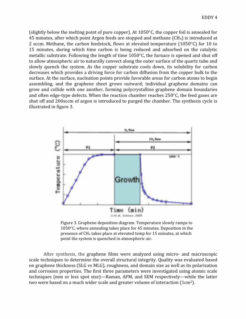
(slightly below the melting point of pure copper). At 1050°C, the copper foil is annealed for 45 minutes, after which point Argon feeds are stopped and methane (CH4) is introduced at 2 sccm. Methane, the carbon feedstock, flows at elevated temperature (1050°C) for 10 to 15 minutes, during which time carbon is being reduced and adsorbed on the catalytic metallic substrate. Following the length of time 1050°C, the furnace is opened and shut off to allow atmospheric air to naturally convect along the outer surface of the quartz tube and slowly quench the system. As the copper substrate cools down, its solubility for carbon decreases which provides a driving force for carbon diffusion from the copper bulk to the surface. At the surface, nucleation points provide favorable areas for carbon atoms to begin assembling, and the graphene sheet grows outward; individual graphene domains can grow and collide with one another, forming polycrystalline graphene domain boundaries and often edge-type defects. When the reaction chamber reaches 250°C, the feed gases are shut off and 200sccm of argon is introduced to purged the chamber. The synthesis cycle is illustrated in figure 3.
After synthesis, the graphene films were analyzed using micro- and macroscopic scale techniques to determine the overall structural integrity. Quality was evaluated based on graphene thickness (SLG vs MLG), roughness, and domain size as well as its polarization and corrosion properties. The first three parameters were investigated using atomic scale techniques (mm or less spot size)—Raman, AFM, and SEM respectively—while the latter two were based on a much wider scale and greater volume of interaction (1cm2).
Figure 3. Graphene deposition diagram. Temperature slowly ramps to 1050°C, where annealing takes place for 45 minutes. Deposition in the presence of CH4 takes place at elevated temp for 15 minutes, at which point the system is quenched in atmospheric air.

EDDY 5
Results and Discussion
Samples were characterized using Scanning Electron Microscopy (SEM) analysis. Pretreatment of copper with acetic acid (AA) serves to clean the surface of metal contaminants and particles, but figure 4 a) show it does not remediate the cold rolling striations that lead to graphene edge defects and MLG [13]. Further annealing b) helped to smooth the surface, however the striation lines are still evident. The results of deposition c,d) show wavy ‘ripples’ indicating the presence of graphene, however they occur in patches and lack uniformity. These images indicate that acetic acid treatment does not significantly assist in the formation of SLG films of good quality, when compared to graphene films grown on bare, untreated copper, as-received from the manufacturer.
Electropolishing (EP) of copper, shown in figure 5 a), effectively eliminates all traces of cold rolling striations and dramatically decreases the roughness of the copper substrate and correnspondingly the graphene sheet above. Graphene ripples seen in b) are highly regular and can be seen to cover the entire image. The triple junction in c) also shows good film quality, however the underlying copper grain area concentrated at the triple junction facilitated some secondary nucleation d) and led to limited MLG deposition. Electropolishing is the preferred pretreatment method for establishing a graphene synthesis method that produces predomiantly SLG films of good uniformity
a
c d
b
a
c d
b

EDDY 6
Raman analysis provides more information about SLG and MLG fractions. Laser excitation during Raman creates two major peaks at 1580 cm-1 and 2690 cm-1, known as the G and CD peaks respectively. The G peak is the primary signature resulting from in-plane vibrational modes, and 2D is a two-phonon coupled peak. The ratio of intensities I2D/IG reveals the number of graphene layers [15]. Figure 5 has values for the I2D/IG of acetic acid treatment (blue) and electropolishing (red) of 1.45 and 1.39 respectively. Both values suggest a mixed character of both SLG and MLG from further carbon supply penetration.
Atomic Force Microscopy (AFM) analysis shows that EP has drastically lower roughness values (figure 7) than AA treatment, which is in agreement with the SEM imaging as described before.
EDDY 7
Corrosion tests
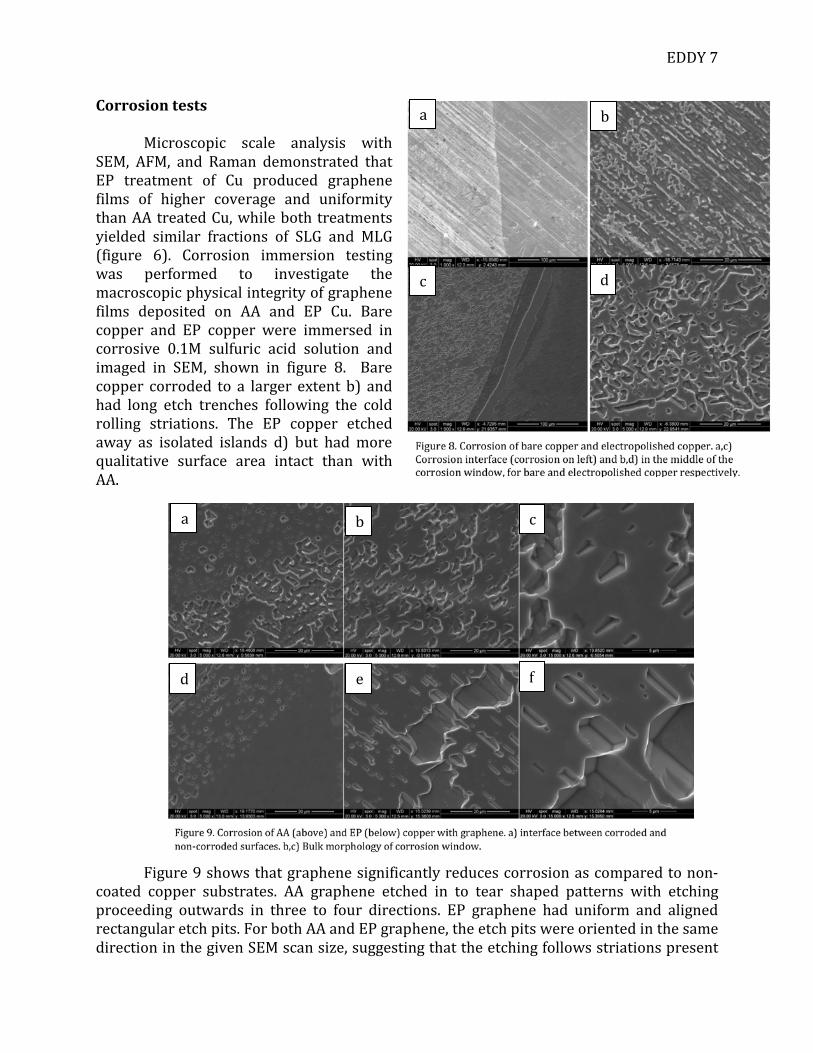
Microscopic scale analysis with SEM, AFM, and Raman demonstrated that EP treatment of Cu produced graphene films of higher coverage and uniformity than AA treated Cu, while both treatments yielded similar fractions of SLG and MLG (figure 6). Corrosion immersion testing was performed to investigate the macroscopic physical integrity of graphene films deposited on AA and EP Cu. Bare copper and EP copper were immersed in corrosive 0.1M sulfuric acid solution and imaged in SEM, shown in figure 8. Bare copper corroded to a larger extent b) and had long etch trenches following the cold rolling striations. The EP copper etched away as isolated islands d) but had more qualitative surface area intact than with AA.
Figure 9 shows that graphene significantly reduces corrosion as compared to non-coated copper substrates. AA graphene etched in to tear shaped patterns with etching proceeding outwards in three to four directions. EP graphene had uniform and aligned rectangular etch pits. For both AA and EP graphene, the etch pits were oriented in the same direction in the given SEM scan size, suggesting that the etching follows striations present
a
c d
b
a
d e
b
f
c

EDDY 8
in the graphene surface that arose during cooling due to the mismatch of coefficients of thermal expansion for copper verse graphene. Selecting etching in localized pits is taking place above underlying polycrystalline grains, suggesting that solvent and corrosive molecules are penetrating at boundaries in graphene domains and attacking the underlying copper substrate, however the corrosive species are unable to travel further along the graphene-copper interface and completely etch copper. These findings are in agreement with previous work of Hsieh et al. [4] and with kinetics models proposed by Kidambi et al. [13].
Fullerene nanoassembly on graphene lattices
Fullerene deposition processes rely on dissolving powderized fullerenes in solution and ‘dip’ coating copper with graphene films into solution for a given amount of time. Isolated fullerene surrounded by a solvent shell migrate toward the graphene surface and nucleate due to similar lattice structures between the sp2 fullerene and graphene. Additional fullerenes reach the nucleation site and form nano-scale assemblies with very high surface area and varying degrees of porosity. Fullerene deposition depends on the concentration in solution, solvent evacuation method, and solvent-fullerene interactions depending on solubility [16]. Three graphene samples were grown on electropolished copper using the established graphene synthesis method, dip coated in a 2mg/ml fullerene solution in tetralin, carbon disulfide (CS2), and 1-2 dichlorobenzene, and heated on a hot plate at 100°C until all solvent had been driven from the substrate.
Figure 10 shows the sample prepared with fullerenes in 1-2 dichlorobenzene. Some solvent was visible on the surface of the sample in a concentrated solvent ‘dome’ in the center and a thin film surrounding. The film evaporated immediately, and after a few seconds of vibrating the solvent bubble spontaneously and energetically evaporated, leaving behind a visible residue along the edges of the solvent bubble. Inspection using SEM under high magnification revealed that the 1-2 dichlorobenzene solution encouraged fullerene assembly in a hexagonal-cross like fashion b,c). 50,000x magnification shows a flower structure with a seemingly hollow middle. The 6 ‘arms’ seen in d) radiate out from the middle and have distinct edges.
a
c d
b

EDDY 9
Samples prepared with tetralin solution exhibited a similar behavior upon heated evaporation. The solvent formed a large bubble on the substrate surface and vibrated violently when the sample first contacted the hot plate. After a few seconds, the solvent bubble began to evaporate along the edges of the bubbles in a circular fashion around the perimeter. Figure 11 a) shows a characteristic ‘S’ shape left behind as a result. The top of the ‘S’ feature in b,c) shows a rounded, smooth morphology of several distinct sizes. Images along the bottom row of figure 11, d,e,f) were taken from the center of the ‘S’ area. The fullerene nanoassembly morphology is short order coordinated circular structures. Image f) shows that coverage at 50,000x magnification is highly uniform. Tetralin appears to be apromising solvent for fullerene deposition because a highly uniform film of fullerenes is required for electrode and other electrochemical applications. Both 1-2 dichlorobenzene and tetralin solutions yielded fullerene structures that were predominantly flat and 2D in character, with independent and unique subunits assembling into larger structures on multiple different length scales. High fractions of fullerene coverage in the selected ares analyzed using SEM were observed for both samples.
a
d e
b
f
c

EDDY 10
Carbon disulfide (CS2) has the lowest flashpoint of the three chemicals used, and consequently upon transferring the sample from the CS2 solution to the hotplate the solvent flashed and produced a flame. Figure 12 shows that at 1,000x magnification a,b), the coverage is consistent across the scan area. White specks are visible in all images and are a likely particulate residue from the combustion reaction. Images c,d) are high magnification views of the area in b) and indicate the fullerene nanoassemblies have a needle-like protruding structure; the structures are highly 3D in nature and possess many distinct needles that create large porosity and the possibility of extensive channeling along and even within needles, provided a number of them are hollow. Extremely high temperatures experienced near the surface within the flame imparted fast velocities to the solvent molecules and some local velocity normal to the surface for fullerene molecules still influenced by solvation. Fullerenes influenced with vertical velocity to the surface proceeded to assemble in columnar fashion into tall needles.
a
c d
b

EDDY 11
Conclusions
Chemical vapor deposition on copper has been shown to be significantly affected by the underlying, inherent copper substrate grain structure. Defect-rich areas in as-grown graphene films concentrate on top of copper polycrystalline grains and around local graphene polycrystalline grains. Ripples characteristics to graphene grown on copper systems, due to the mismatch of coefficient of thermal expansion between the two incoherent phases, causing parallel ‘cracking’ on graphene along the ripple ridges. These defects, and the channels created under ripple ridges, allow solvent and etchant molecules to penetrate the graphene surface and etch the copper below, leading to the inability of graphene to act as an integral physical barrier film. Targeted pretreatment of copper was investigated to selectively reduce copper cold-rolling striations and produce a smoother surface. Acetic acid cleaning was proven to be an ineffective method to reduce roughness, as compared to electropolishing in phosphoric acid. Graphene grown on EP copper exhibited substantially lower corrosion rates, versus similarly processed samples without graphene. Localized corrosion did occur, however, in the defect-dense regions described previously. Further experimentation needs to be done to attempt to produce very low-defect, low-roughness graphene films with a high degree of uniformity.
Fullerene-composite structures assembled on EP graphene possessed a large degree surface coverage and, depending on the solvent utilized for deposition, had a unique subunit geometry that was repeated on several length scales. 1-2 dichlorobenzene, tetralin, and CS2 all successfully dissolved 2mg/ml fullerene solutions and facilitated fullerene nanoassembly generation. 1-2 dichlorobenzene and tetralin had mostly flat, 2D fullerene features, whereas CS2 encourage formation high aspect ratio, sharp needle-like rods that coordinated in 3D meta-structures. The large porosity and surface area characteristic to the fullerene assemblies produced during experimentation provide strong evidence for potential applications in electrochemistry and electronics and use as an electrode in batteries and supercapacitors.
Further testing needs to be conducted with the 1-2 dichlorobenzene, tetralin, and CS2 by varying the concentration of dissolved fullerenes in solution (up to a solvent’s respective solubility limit), incorporating a substituted delivery method of micropipette ‘drop’ coating to introduce a controlled dome-shaped deliver with nearly constant volume, and incrementally lowering the hot plate temperature to facilitate a more moderate evaporate. The goal is to achieve uniform fullerene deposition of highly coordinates structures across the entire graphene surface with large surface area and porosity.
Acknowledgements
I would like to thank my advisor Dr. Krishna Muralidharan and his Ph.D. student Tony Jefferson Gnanaprakasa for their considerable help throughout my senior design process with my research and experimentation. I would also like to thank Dr. Srini Raghavan and his undergraduate research assistant Yuanxi Gu for their assistance with chemical pretreatment of copper and corrosion immersion testing. Thanks also to Dr. Brooke Beam and the Keck center for making their SEM available to me throughout my project.

EDDY 12
References:
1. "Graphene: World-leading Research and Development." ManchesterGraphene (The University of Manchester). N.p., n.d. Web. 2 May 2014. http://www.graphene.manchester.ac.uk/story/properties/ 2. Blendis, Stefanie, and Frances Perraudin. "Graphene: 'Miracle material' willbe in your home sooner than you think." CNN. Cable News Network, 1 Jan. 1970. Web. 2 May 2014. <http://www.cnn.com/2013/10/02/tech/innovation/graphene-quest-for-first-ever-2d-material/>. 3. Gray D. et al. Crystal Structure of Graphite, Graphene and Silicon. 6.730—Physics for Solid State Applications. 2009. 4. Chung D. Electrical applications of carbon materials. Journal of MaterialsScience 39 2645– 2661 2004. 5. Hsieh Y. et al. Complete Corrosion Inhibition through Graphene DefectPassivation. ACSnano vol 8. No1. 443-448. 2014 6. Gnanaprakasa T. Bottom-up Surface Engineering of DNA Macro-assembliesfor Nanoelectronics and Optical Biosensors. Auburn University. May 2011 7. Zhu Y. et al. Carbon-Based Supercapacitors Produced by Activation ofGraphene. SCIENCE VOL 332 JUNE 2011 8. "Fullerenes: An Overview." Fullerenes: An Overview. N.p., n.d. Web. 2 May2014. <http://www.ch.ic.ac.uk/local/projects/unwin/Fullerenes.html>. 9. "Fullerene." HowStuffWorks. HowStuffWorks.com, 22 July 2009. Web. 2 May2014. <http://science.howstuffworks.com/dictionary/chemistry-terms/fullerene-info.htm>. 10. "Fullerenes and Buckeyballs" . N.p., n.d. Web. 2 May 2014.<http://research.che.tamu.edu/groups/Seminario/materials/G04_Buckyballs.pdf> 11. Huttinger et al. Mechanisms of carbon deposition—a kinetic approach.Carbon 40 617–636 (2002) 12. Huttinger et al. K inetics of surface reactions in carbon deposition from lighthydrocarbons. Carbon 41 1509–1514 (2003) 13. Kidambi P. et al. The Parameter Space of Graphene Chemical VaporDeposition on Polycrystalline Cu. J. Phys. Chem. C 116, 22492−22501 (2012). 14. Zhang Y. Review of Chemical Vapor Deposition of Graphene and RelatedApplications. ACS 2329–2339 ’ 2013 15. Childres I. et al. Raman Spectroscopy of Graphene and Related Materials.Purdue University 16. Ruoff R. S. et al. Solubility of C60 in a Variety of Solvents. J. Phys. Chem 97,3379-3383 (1993)

EDDY 13
Appendix Courtesy of undergraduate MSE student Yuanxi Gu who assisted my research group with copper pretreatment and corrosion immersion testing protocols.
Acetic Acid Treatment of Copper Foil. Copper samples were prepared from a sheet of 250 μm thick copper foil purchased from Sigma-Aldrich Co., LLC (99.98%, product code 349178-49.5G). Copper sample was cut into 1.5 cm by 2 cm and was rinsed by acetone followed by methanol for 30 seconds for each. Then, nitrogen dried copper sample was immersed in acetic acid (glacial HPLC, FisherChemicals, product code AC22214000) with heating up at 50 °C for 10 minutes. The copper sample was then rinsed with DI water and dried with nitrogen gas.
Electropolishing Treatment of Copper Foil. Copper samples were prepared from copper foil with the same origin, and were cut into 1.5 cm by 3 cm pieces. Sample was rinsed by isopropyl alcohol for 30 seconds, following by deionized water rinsing and nitrogen drying. The sample was then introduced into electrochemical cell with a three-electrode system. One sample at a time was placed into the electrochemical cell as working electrode, with a platinum foil counter electrode and a mercury/mercurous sulfate reference electrode. All of three electrodes were submersed in an electrolyte which is an 85% phosphoric acid solution (Honeywell, product code 10181851). After being attached to a galvanostat (Princeton Applied Research 273A), a constant anodic current was applied to the working electrode for the duration of electropolishing treatment, with a current density of 0.075 Amps/cm2 for one hour. Figure 1 shows a simplified sketch of the experimental setup. After EP treatment, the sample was cleaned with deionized water and dried with nitrogen gas.
Figure 1. Sketch of electrochemical cell with a three-electrode system.
Electrochemical tests A simple immersion corrosion test was also performed to compare topographical
features. Graphene coated samples using two pretreatments were immersed into a corrosive solution comprising 0.1 M sulfuric acid and 1 μM copper sulfate for 5 minutes. After removing from the corrosive solution, samples were cleaned with deionized water and dried with nitrogen gas.