
Chemical-mechanical polishing process development for...
89
Erasmus Mundus MSc in Photonics Erasmus Mundus Chemical-mechanical polishing process development for III-V/SOI waveguide circuits Muhammad Muneeb Promotor(s)/Supervisor(s): prof. dr. ir. Dries Van Thourhout, dr. ir. Günther Roelkens Assisting supervisor(s): Stevan Stankovic Master dissertation submitted in order to obtain the academic degree of Erasmus Mundus Master of Science in Photonics Academic year 2009-2010
Transcript of Chemical-mechanical polishing process development for...
Erasmus Mundus MSc in Photonics
Erasmus Mundus
Chemical-mechanical polishing process development for III-V/SOI waveguide circuits
Muhammad Muneeb
Promotor(s)/Supervisor(s): prof. dr. ir. Dries Van Thourhout, dr. ir. Günther Roelkens Assisting supervisor(s): Stevan Stankovic
Master dissertation submitted in order to obtain the academic degree of
Erasmus Mundus Master of Science in Photonics
Academic year 2009-2010

Muhammad Muneeb
III-V/SOI waveguide circuitsChemical-mechanical polishing process development for
Academiejaar 2009-2010Faculteit IngenieurswetenschappenVoorzitter: prof. dr. ir. Daniël De ZutterVakgroep Informatietechnologie
Erasmus Mundus Master of Science in PhotonicsMasterproef ingediend tot het behalen van de academische graad van
Begeleider: Stevan StankovicPromotoren: prof. dr. ir. Dries Van Thourhout, dr. ir. Gnther Roelkens


Toelating tot bruikleen De auteur geeft de toelating dit afstudeerwerk voor consultatie beschikbaar te stellen en delen van het afstudeerwerk te copieren voor persoonlijk gebruik. Elk ander gebruik valt onder de beperkingen van het auteursrecht, in het bijzonder met betrekking tot de verplichting de bron uitdrukkelijk te vermelden bij het aanhalen van resultaten uit dit afstudeerwerk. Permission for usage (English version) The author gives his permission to make this work available for consultation and to copy part of the work for personal use. Any other use is bound to the restriction of copyright legislation, in particular regarding the obligation to specify the source when using results of this work. Muhammad Muneeb 2nd June 2010

Acknowledgements First of all I would like to show my gratitude to my supervisor Stevan Stankovic for his
endless and kind support throughout this project work. I am really thankful to him for his
patience during writing of this thesis.
I would like to thank Gunther Roelkens for his valuable inputs and especially his precious
time .
Thanks to my promoter Professor Dries Van Thourhout for believing in me and especially
providing the financial support for this project work.
Special thanks for support and funding from EMMP consortium.
Thanks to all my colleagues and friends .
Lastly, I would like to thank my beloved sister for all her moral support and encouragement.
ABSTRACT
Hybrid integration of III-V materials with Silicon-On-Insulator (SOI) platform is a promising
strategy for fabrication of active photonic devices and adhesive bonding, based on
divinylsiloxane-bis-benzocyclobutene (DVS-BCB or BCB, for short), emerges as a technique
which is suitable for industrial-scale implementation of such an integration. Evanescent
coupling offers a lot of advantages in design and fabrication of these hybrid devices, but for
an efficient coupling, a very thin (several tens of nanometers) and uniform bonding layer is
required. However, due to a poor planarization of BCB on SOI waveguide structures, it is
very challenging to achieve such a thin layer. In this study, we investigate chemical
mechanical planarization (CMP) of BCB in order to allow making of ultra-thin bonding layers
on such a planarized surface. Design of experiments approach was adopted to study the effect
of different slurry compositions, polishing pads and process parameters on BCB planarization.
Using such a developed CMP process, we planarized a BCB layer deposited on a SOI
waveguide circuit and successfully bonded a III-V die to such a planarized SOI waveguide.
Total thickness of a BCB layer after the bonding was 200 nm, while the thickness of a
bonding layer itself was 30 nm.
Keywords: Evanescent coupling, adhesive bonding, BCB, chemical mechanical
planarization, degree of planarization
Chemical-Mechanical Polishing Process Development for III-V/SOI Waveguide Circuits
Muhammad Muneeb
Supervisor: ir. Stevan Stankovic Promotors: Dr. ir. Günther Roelkens , Prof. Dr. ir. Dries Van Thourhout
ABSTRACT
Hybrid integration of III-V materials with Silicon-On-Insulator (SOI) platform is a promising strategy for fabrication of active photonic devices and adhesive bonding, based on divinylsiloxane-bis-benzocyclobutene (DVS-BCB or BCB, for short), emerges as a technique which is suitable for industrial-scale implementation of such integration. Evanescent coupling offers a lot of advantages in design and fabrication of these hybrid devices, but for an efficient coupling, a very thin (several tens of nanometers) and uniform bonding layer is required. However, due to a poor planarization of BCB on SOI waveguide structures, it is very challenging to achieve such a thin layer. In this study, we investigate chemical mechanical planarization (CMP) of BCB in order to allow making of ultra-thin bonding layers on such a planarized surface. Design of experiments approach was adopted to study the effect of different slurry compositions, polishing pads and process parameters on BCB planarization. Using such a developed CMP process, we planarized a BCB layer deposited on a SOI waveguide circuit and successfully bonded a III-V die to such a planarized SOI waveguide. Total thickness of a BCB layer after the bonding was 200 nm, while the thickness of a bonding layer itself was 30 nm. Keywords: Evanescent coupling, adhesive bonding, BCB, chemical mechanical planarization, degree of planarization
1. INTRODUCTION
Silicon photonics emerges as very promising research field which enables large-scale fabrication of passive and some active devices in integrated photonics. However, silicon is hampered by its indirect bandgap which makes it unsuitable for fabrication of light sources. One solution to this problem is hybrid integration of silicon with III-V semiconductors. In hybrid integration, a III-V semiconductor is bonded on top of SOI waveguide circuits. Active photonic functions (light emission, amplification) are performed by III-V material while passive functions (routing, filtering) are done by SOI waveguide structures. To couple the light between SOI waveguides and III-V semiconductor, different coupling schemes can be used and evanescent coupling is a frequently used technique. A number of active photonics devices, based on evanescent coupling and BCB adhesive bonding have been demonstrated [10, 11]. However, evanescent coupling is very sensitive to BCB bonding layer thickness and uniformity. Very thin bonding layers (several tens of nanometers) with excellent planarization are required and this still remains a challenging technical problem. One promising solution to this obstacle is the subject of this master thesis.
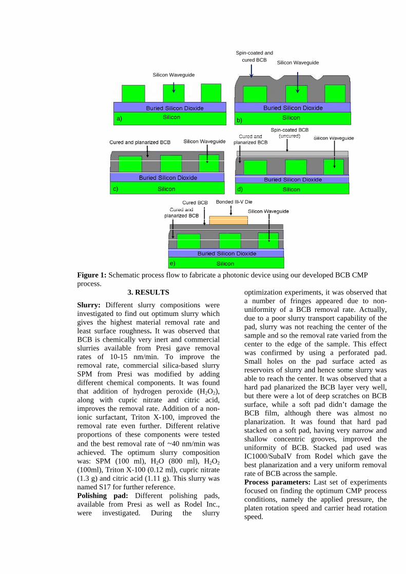
Development of a reliable and reproducible process for the fabrication of very thin BCB bonding layers will pave the way not only for the compact, hybrid silicon lasers, but for the development of other promising photonic devices, such as optical isolators or amplifiers, based on evanescent coupling. In the following sections, we present the development of a BCB CMP process, aimed to achieve thin and planarized BCB films. Figure 1 shows schematically the process flow to fabricate an active photonic device using the developed BCB CMP process.
2. EXPERIMENTS
BCB formulation Cyclotene 3022-35 was spin-coated on the blank silicon as well as patterned SOI samples. Adhesion promoter AP3000 was used before spin-coating. BCB was cured at 250oC for 1 hour in N2 ambient. Contact profilometer from Taylor-Hobson and Optical profilometer Wyko NT3300 were used for pre-CMP and post-CMP measurements. Mecapol P400 polishing tool from Presi was used for CMP experiments. Experiments were organized in three sets. The first set of experiments was aimed to find the optimum slurry composition; the second set was targeted at finding the optimum polishing pad, while the goal of the final set of experiments was to optimize process parameters.
Silicon Waveguide
Spin-coated and cured BCB Silicon Waveguide
a)
e)
d)c)
b)
Silicon Waveguide
Spin-coated and cured BCB Silicon Waveguide
a)
e)
d)c)
b)
Figure 1: Schematic process flow to fabricate a photonic device using our developed BCB CMP process.
3. RESULTS
Slurry: Different slurry compositions were investigated to find out optimum slurry which gives the highest material removal rate and least surface roughness. It was observed that BCB is chemically very inert and commercial slurries available from Presi gave removal rates of 10-15 nm/min. To improve the removal rate, commercial silica-based slurry SPM from Presi was modified by adding different chemical components. It was found that addition of hydrogen peroxide (H2O2), along with cupric nitrate and citric acid, improves the removal rate. Addition of a non-ionic surfactant, Triton X-100, improved the removal rate even further. Different relative proportions of these components were tested and the best removal rate of ~40 nm/min was achieved. The optimum slurry composition was: SPM (100 ml), H2O (800 ml), H2O2 (100ml), Triton X-100 (0.12 ml), cupric nitrate (1.3 g) and citric acid (1.11 g). This slurry was named S17 for further reference. Polishing pad: Different polishing pads, available from Presi as well as Rodel Inc., were investigated. During the slurry
optimization experiments, it was observed that a number of fringes appeared due to non-uniformity of a BCB removal rate. Actually, due to a poor slurry transport capability of the pad, slurry was not reaching the center of the sample and so the removal rate varied from the center to the edge of the sample. This effect was confirmed by using a perforated pad. Small holes on the pad surface acted as reservoirs of slurry and hence some slurry was able to reach the center. It was observed that a hard pad planarized the BCB layer very well, but there were a lot of deep scratches on BCB surface, while a soft pad didn’t damage the BCB film, although there was almost no planarization. It was found that hard pad stacked on a soft pad, having very narrow and shallow concentric grooves, improved the uniformity of BCB. Stacked pad used was IC1000/SubaIV from Rodel which gave the best planarization and a very uniform removal rate of BCB across the sample. Process parameters: Last set of experiments focused on finding the optimum CMP process conditions, namely the applied pressure, the platen rotation speed and carrier head rotation speed.
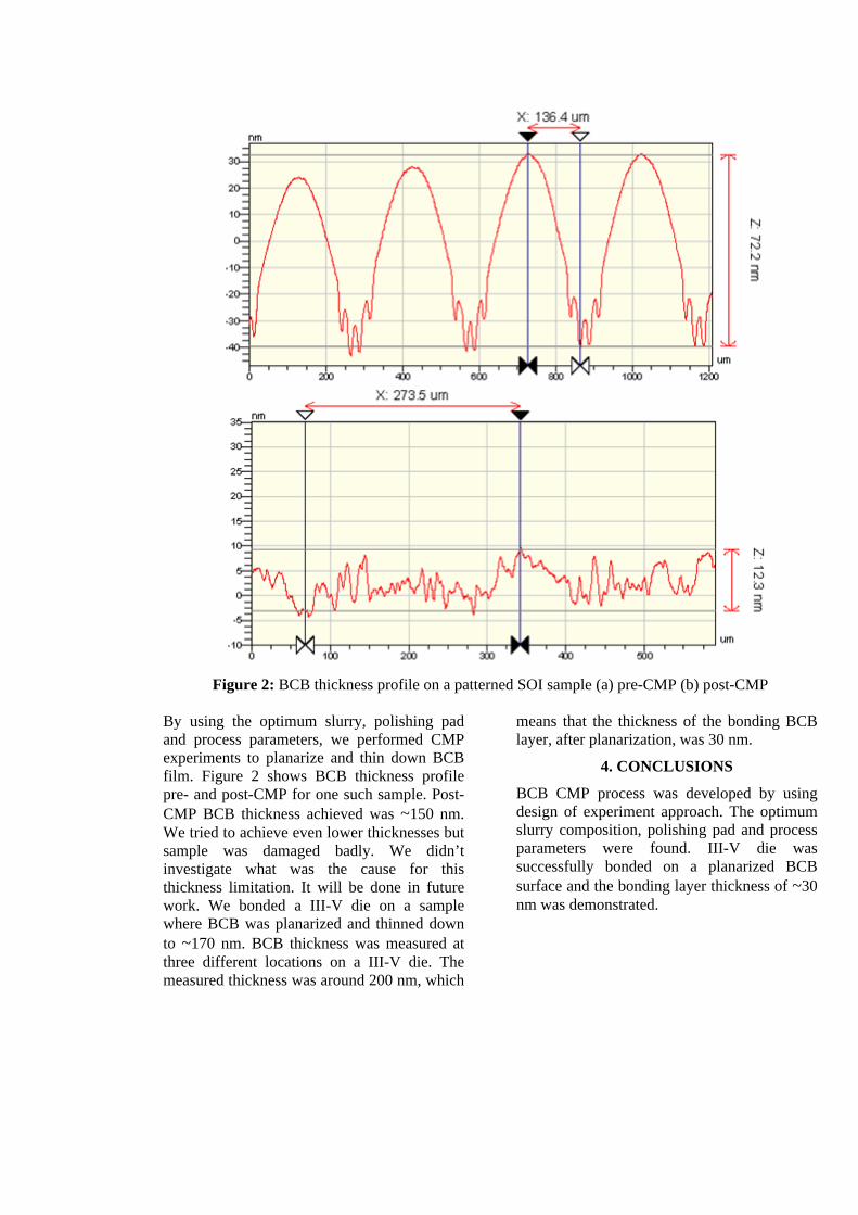
Figure 2: BCB thickness profile on a patterned SOI sample (a) pre-CMP (b) post-CMP
By using the optimum slurry, polishing pad and process parameters, we performed CMP experiments to planarize and thin down BCB film. Figure 2 shows BCB thickness profile pre- and post-CMP for one such sample. Post-CMP BCB thickness achieved was ~150 nm. We tried to achieve even lower thicknesses but sample was damaged badly. We didn’t investigate what was the cause for this thickness limitation. It will be done in future work. We bonded a III-V die on a sample where BCB was planarized and thinned down to ~170 nm. BCB thickness was measured at three different locations on a III-V die. The measured thickness was around 200 nm, which
means that the thickness of the bonding BCB layer, after planarization, was 30 nm.
4. CONCLUSIONS
BCB CMP process was developed by using design of experiment approach. The optimum slurry composition, polishing pad and process parameters were found. III-V die was successfully bonded on a planarized BCB surface and the bonding layer thickness of ~30 nm was demonstrated.
I
Table of Contents
1 INTRODUCTION..............................................................................................................1
1.1 Aim of the Project ......................................................................................................2
2 CMP BASICS ....................................................................................................................4
2.1 Why CMP?.................................................................................................................4
2.2 The CMP Process .......................................................................................................4
2.2.1 Preston’s Model..................................................................................................6
2.2.2 Planarization.......................................................................................................7
2.3 CMP Tools .................................................................................................................8
2.3.1 Polishing Head / Wafer Carrier Design..............................................................9
2.4 CMP Consumables ...................................................................................................11
2.4.1 Polishing Pads ..................................................................................................11
2.4.2 Conditioning Diamonds ...................................................................................14
2.4.3 Slurry ................................................................................................................15
2.5 CMP Process Issues..................................................................................................17
2.5.1 Scratches...........................................................................................................18
2.5.2 Pattern Density Variation .................................................................................18
2.5.3 Dishing and Erosion Effect ..............................................................................19
2.6 Post-CMP Cleaning..................................................................................................19
3 BCB CMP PROCESS ......................................................................................................21
3.1 BCB Properties.........................................................................................................21
3.1.1 Chemical structure............................................................................................21
3.1.2 Properties..........................................................................................................21
3.1.3 Spin-Coating.....................................................................................................22
3.1.4 Curing...............................................................................................................25
3.1.5 Defects After Curing ........................................................................................27
3.2 Chip Layout Description ..........................................................................................29
II
3.3 Pre-CMP Planarization of BCB ...............................................................................30
3.4 BCB CMP ISSUES ..................................................................................................34
3.5 Literature Review.....................................................................................................36
4 CMP of BCB: Our Approach ...........................................................................................38
4.1 Our Approach ...........................................................................................................38
4.2 Our CMP Tool..........................................................................................................40
4.3 Tools of Analysis......................................................................................................42
4.3.1 FIB Cross-sectioning........................................................................................43
4.3.2 Scratch method .................................................................................................44
5 CMP OF BCB: EXPERIMENTS AND RESULTS.........................................................48
5.1 Slurry Optimization: Experiments and Results ........................................................49
5.2 Polishing Pad Optimization: Experiments and Results ............................................52
5.3 CMP Process Parameters Optimization: Experiments and Results..........................56
6 POST-CMP PROCESSING: PHOTODETECTOR FABRICATION.............................62
7 CONCLUSIONS AND PROSPECTS FOR FUTURE WORK.......................................66
7.1 Conclusions ..............................................................................................................66
7.2 Prospects for Future Work .......................................................................................66
REFERENCES.........................................................................................................................68
III
List of Figures
Figure 1.1 Evanescently-coupled device fabrication process (cross-section view): (a) SOI waveguide circuit; (b) spin-coating and curing of BCB; (c) planarization of BCB by CMP; (d) spin-coating of the second (bonding) BCB layer; (e) machine-based bonding of a III-V die ...2
Figure 2.1 (a) Device fabrication without planarization (b) fabrication with planarization [12]....................................................................................................................................................4
Figure 2.2 Schematic view of the CMP equipment [15] ...........................................................5
Figure 2.3 Schematic view of Silicon dioxide CMP process [15].............................................5
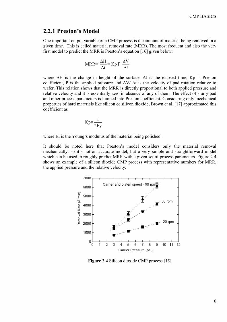
Figure 2.4 Silicon dioxide CMP process [15] ...........................................................................6
Figure 2.5 Schematic showing the applied pressure distribution [15] ......................................7
Figure 2.6 Measure of Planarity [18] ........................................................................................7
Figure 2.7 Schematic representation for different degrees of planarization [13] ......................8
Figure 2.8 Schematic view of a rotary type CMP tool ..............................................................9
Figure 2.9 Schematic view of CMP carrier [15] .....................................................................10
Figure 2.10 Schematic view of a carrier design with spatially distributed applied pressure [21] ...........................................................................................................................................10
Figure 2.11 SEM image of a wafer in contact with pad asperities [15] ..................................12
Figure 2.12 Schematic view of a pad-wafer interaction: (Left) soft compressible pad (Right) Hard stiff pad [15] ....................................................................................................................13
Figure 2.13 Schematic cross section of a multilayer polishing pad [22]................................13
Figure 2.14 Fixed abrasive pad: (Left) Schematic view (Right) Schematic view of top surface with fixed abrasives [15] ..........................................................................................................14
Figure 2.15 SEM image of IC1000 polishing pad: (a) before; (b) after the polishing [23].....14
Figure 2.16 Removal rate revival after the use of conditioning during CMP process [20].....15
Figure 2.17 SEM image of a IC1000 polishing pad, partially covered with 200 nm size abrasive particles [25] ..............................................................................................................15
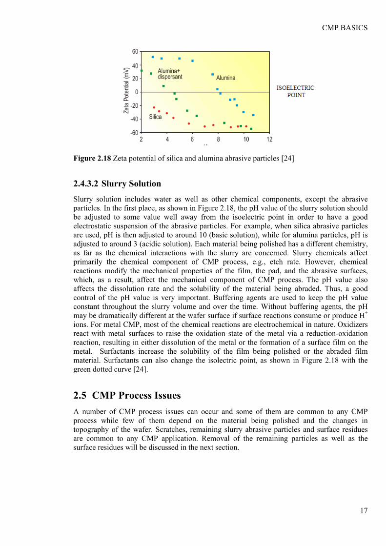
Figure 2.18 Zeta potential of silica and alumina abrasive particles [24].................................17
Figure 2.19 Three states of silica abrasive particle [20]..........................................................18
Figure 2.20 Effect of pattern density variation on planarization [15] .....................................18
Figure 2.21 Schematic illustration of the dishing effect [15] ..................................................19
IV
Figure 2.22 Schematic view of the erosion effect [15]............................................................19
Figure 2.23 Schematic illustration of a brush cleaning system [15] ......................................20
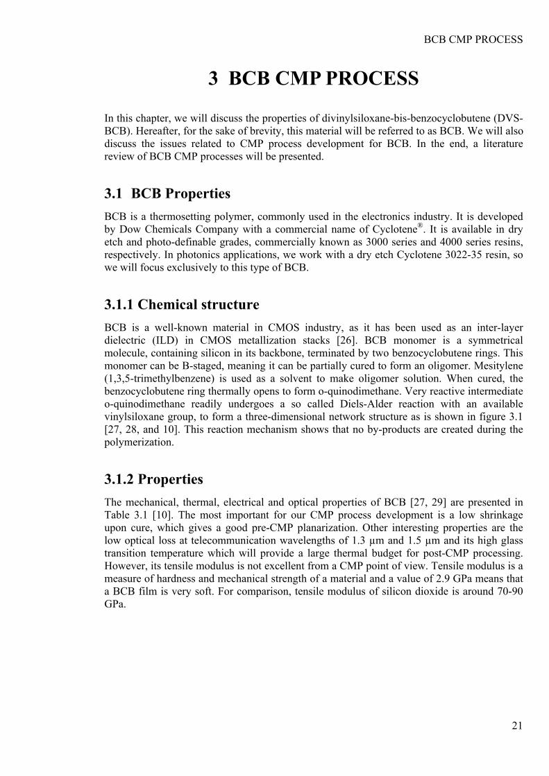
Figure 3.1 DVS-BCB monomer and polymerization mechanism [10] ...................................22
Figure 3.2 Spin curves for various commercially available BCB formulations [10] ..............23
Figure 3.3 BCB thickness versus added mesitylene fraction compared to pure BCB volume [10] ...........................................................................................................................................23
Figure 3.4 Particles contaminated blank silicon samples after spin-coating BCB..................24
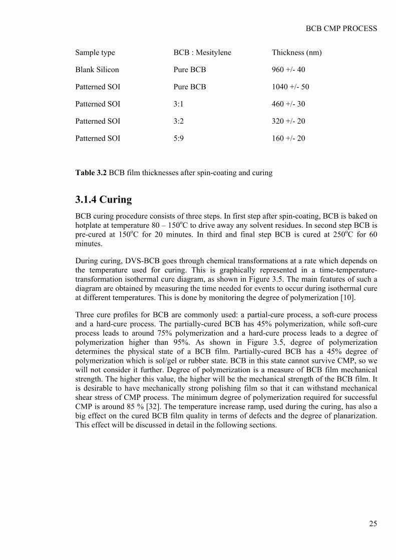
Figure 3.5 Extent of BCB cure (degree of polymerization) as function of temperature and time [31] ...................................................................................................................................26
Figure 3.6 BCB curing profile A.............................................................................................26
Figure 3.7 BCB curing profile B ............................................................................................27
Figure 3.8 Post-cure defect - a crater: (a) 3D view; (b) 2D view with markers; (c) profile along the horizontal line (x-axis); (d) profile along the vertical line (y-axis) ..........................28
Figure 3.9 GDS mask layout of a chip used for CMP experiments .......................................29
Figure 3.10 Portion of the chip layout containing a set of spectrometers [34]........................30
Figure 3.11 The structure of waveguides: (a) dark field waveguide; (b) photonic wire ........30
Figure 3.12 Planarization of the waveguides with a 300 microns pitch: (a) 2-D contour plot with the markers; (b) BCB profile along the x-axis .................................................................31
Figure 3.13 Planarization of the waveguides with a 25 micron pitch: (a) 2-D contour plot with the markers; (b) BCB profile along the x-axis .................................................................32
Figure 3.14 Planarization of the waveguides with a 50 micron pitch, cured using the curing profile B: (a) 2-D contour plot with the markers; (b) BCB profile along the x-axis................33
Figure 3.15 Planarization with a thinner BCB: (a) 2-D contour plot with the markers; (b) BCB profile along the x-axis....................................................................................................33
Figure 3.16 Photonic wire waveguide structure planarization: (a) 3D view; (b) 2D view with the markers; (c) BCB profile along the x-axis; (d) BCB profile along the y-axis....................34
Figure 3.17 Mechanical integrity scale of different dielectrics, normalized to silicon dioxide [36] ...........................................................................................................................................35
Figure 3.18 CMP evaluation of different low-k materials [37]...............................................35
Figure 4.1 A complete set of CMP variables ..........................................................................39
Figure 4.2 CMP tool Mecapol P400........................................................................................40
V
Figure 4.3 Polishing head: (a) backside of sample holder; (b) piston spindle fitted into sample holder........................................................................................................................................40
Figure 4.4 Pad compression at the sample edge [47] ..............................................................41
Figure 4.5 Schematic view of the wax-mounted and free-mounted polishing performance [19]..................................................................................................................................................42
Figure 4.6 A sample wax-mounted on the sample holder for CMP experiment .....................42
Figure 4.7 Dual beam SEM/FEI (FEI Nova 600 Novalab) system .........................................43
Figure 4.8 Schematic representation of the pre-CMP and the post-CMP measurement of BCB film thickness by scratch method .............................................................................................44
Figure 4.9 Contact profilometer (TalyStep) and an example of a measurement where BCB thickness is 980 nm, plotted using a 40 nm/div setting (measurement profile drawn by TalyStep is digitally highlighted for clarity) ............................................................................45
Figure 4.10 (a) Snapshot of optical profilometer (Wyko); (b) a gold deposited sample.........46
Figure 4.11 Wyko measurement of BCB film thickness by using scratch method: (a) 3D view; (b) Horizontal Profile of BCB thickness. .......................................................................47
Figure 5.1 Schematic illustration of our BCB CMP process development experiment cycle.48
Figure 5.2 Delamination of BCB during CMP with various process parameters: (a) pressure = 24.8 kPa, velocity = 45 rpm; (b) pressure = 12.4 kPa, velocity = 45 rpm; (c) pressure = 12.4 kPa, velocity = 30 rpm. ............................................................................................................50
Figure 5.3 BCB CMP results using pressure of 24.8 kPa, velocity of 45 rpm, after: (a) 5 min; (b) 10 min (scratches in BCB films, used for thickness measurements are clearly visible) ...50
Figure 5.4 Polishing pads surface texture: (a) LDR1 plain; (b) LDR1 embossed; (c) SubaIV perforated; (d) Supra5 embossed; (e) PUR; (f) Stacked IC1000/SubaIV ................................54
Figure 5.5 Samples polished on LDR1 polishing pad using different slurries: (a) slurry S7, MRR = 8 nm/min; (b) slurry S3, MRR = 12 nm/min; (c) slurry S8, MRR = 20 nm/min. .......54
Figure 5.6 Difference in polish results using plain and perforated pads: (a) SubaIV plain; (b) SubaIV perforated ....................................................................................................................55
Figure 5.7 Difference in CMP performance between a hard and a soft polishing pad: (a) Politex; (b) PUR .......................................................................................................................56
Figure 5.8 Schematic illustration of the relative velocity vectors for different combinations of carrier head and platen rotation speeds [51].............................................................................57
Figure 5.9 Effect of the difference in platen and head rotation speeds: (a) platen speed of 45 rpm and head speed of 30 rpm; (b) platen speed of 45 rpm and head speed of 20 rpm; (c) both platen and head speeds were 45 rpm, but the sample was mounted off-centered ....................57

VI
Figure 5.10 Experimental verification of Preston’s equation: applied pressure versus MRR58
Figure 5.11 Surface roughness comparison for a patterned SOI sample: (a) before CMP; (b) after CMP .................................................................................................................................59
Figure 5.12 Pre-CMP planarization of BCB on top of the waveguides with 300 microns pitch: (a) 2-D contour plot with markers; (b) horizontal profile of BCB ...........................................59
Figure 5.13 Pre-CMP planarization of BCB on top of the waveguides with 25 microns pitch: (a) 2-D contour plot with markers; (b) horizontal profile of BCB ...........................................60
Figure 5.14 Pre-CMP photonic wire waveguide structure planarization: (a) 3D view; (b) 2D view with markers; (c) BCB x-axis profile; (d) BCB y-axis profile. .......................................60
Figure 5.15 Post-CMP photonic wire waveguide structure planarization: (a) 3D view; (b) 2D view with markers; (c) BCB x-axis profile; (d) BCB y-axis profile. .......................................61
Figure 6.1 Schematic view of the spectrometer [34]..............................................................62
Figure 6.2 MSM photo-detector: (a) 3D view (b) device cross-section [11] ..........................63
Figure 6.3 Absorption as a function of the detector length for different BCB layer thicknesses [11] ...........................................................................................................................................63
Figure 6.4 BCB film thickness after bonding of III-V die to a planarized spectrometer chip: (a) Spot 1, BCB thickness 191.9 nm; (b) Spot 2, BCB thickness 203 nm; (c) Spot 3, BCB thickness 201.5 nm...................................................................................................................65
Abbreviations and Acronyms
Chemical mechanical planarization (CMP)
Benzocyclobutene (BCB)
Complementary metal–oxide semiconductor (CMOS)
Metal-Semiconductor-Metal (MSM)
Silicon-on insulator (SOI)
Depth of focus (DOP)
Material removal rate (MRR)
Pressure (P)
Velocity (V)
Revolutions per minute (rpm)
Root mean square (rms)
Young’s modulus (Ey)
Preston’s coefficient (Kp)
Degree of planarization (DOP)
Step height reduction (SHR)
Non-uniformity (NU)
Center Air Pressure (CAP)
Ripple Air Pressure (RAP)
Outer Air Pressure (OAP)
Edge Air Pressure (EAP)
Tri-methyl ammonium hydroxide (TMAH)
Standard cleaning solution 1 (SC-1)
Graphic Data System (GDS)
Planar concave grating (PCG)
Scanning Electron Microscopy (SEM)
Focused ion beam (FIB)
INTRODUCTION
1
1 INTRODUCTION
Silicon photonics is emerging as a very promising technology for fabrication of various integrated photonic components. The main advantage of silicon photonics is the use of well-established, readily available and relatively inexpensive technology of silicon processing. Silicon is transparent at telecommunication wavelengths of 1.3 µm and 1.55 µm and, therefore, has a great potential for implementation in the next generation of high speed communication photonic devices. However, silicon has an indirect bandgap and that makes fabrication of light emitting and amplifying photonic devices very challenging. Although a number of approaches [1, 2, 3 and 4] have been explored in the past, it is generally agreed that implementation of efficient and reliable active components in silicon is not viable in the near future [5]. One solution to this problem is hybrid integration of direct bandgap III-V semiconductors with SOI waveguide platform. Hybrid integration can be realized by bonding III-V semiconductor dies on top of SOI waveguide structures. This approach combines an efficient light emission from III-V semiconductors with the waveguide structures that are fabricated on SOI platform using well-established, low-cost, high yield CMOS fabrication processes.
Since the purpose of III-V semiconductors in hybrid integration is mainly light emission and/or amplification, while the passive functions are performed in SOI waveguide structures, a technique is required to couple the light between SOI waveguides and III-V active devices. Evanescent coupling is a frequently used technique for this. Hybrid semiconductor lasers based on evanescent coupling, with III-V active layers mounted on top of silicon waveguides by the means of molecular bonding, have been recently demonstrated [6, 7, 8 and 9]. As the bulk of the optical power within the cavities of such lasers is already confined to the silicon waveguide, no additional optical coupling element (such as a taper) is usually required. This enables lasers based on evanescent coupling to be very compact and most suitable for high density integration photonic devices.
However, molecular bonding technique is very sensitive to particle contamination and surface roughness and offers a relatively low yield. Therefore, a heterogeneous integration based on alternative bonding techniques has been actively pursued recently. Adhesive bonding based on divinylsiloxane-bis-benzocyclobutene (DVS-BCB or simply BCB) has been developed by Photonics Research Group of Department of Information Technology (INTEC), at Ghent University, Belgium. Several photonic devices based on BCB adhesive bonding have already been demonstrated [10, 11]. Following this, a joint research project between INTEC’s Photonics Research Group and Intel Corporation’s Photonic Technology Labs has started, which is specifically related to design and fabrication of evanescently-coupled hybrid III-V/silicon laser based on BCB bonding. On the other hand, evanescent coupling requires very thin bonding layers (several tens of nanometers) with excellent planarization and this still remains a serious technical problem that needs to be solved. One promising solution to this obstacle is a subject of this master thesis. Development of a reliable and reproducible process for fabrication of very thin DVS-BCB bonding layers will pave the way not only for the compact, hybrid silicon lasers, but for the development of other promising photonic devices, such as optical isolators or amplifiers, based on evanescent coupling.
INTRODUCTION
2
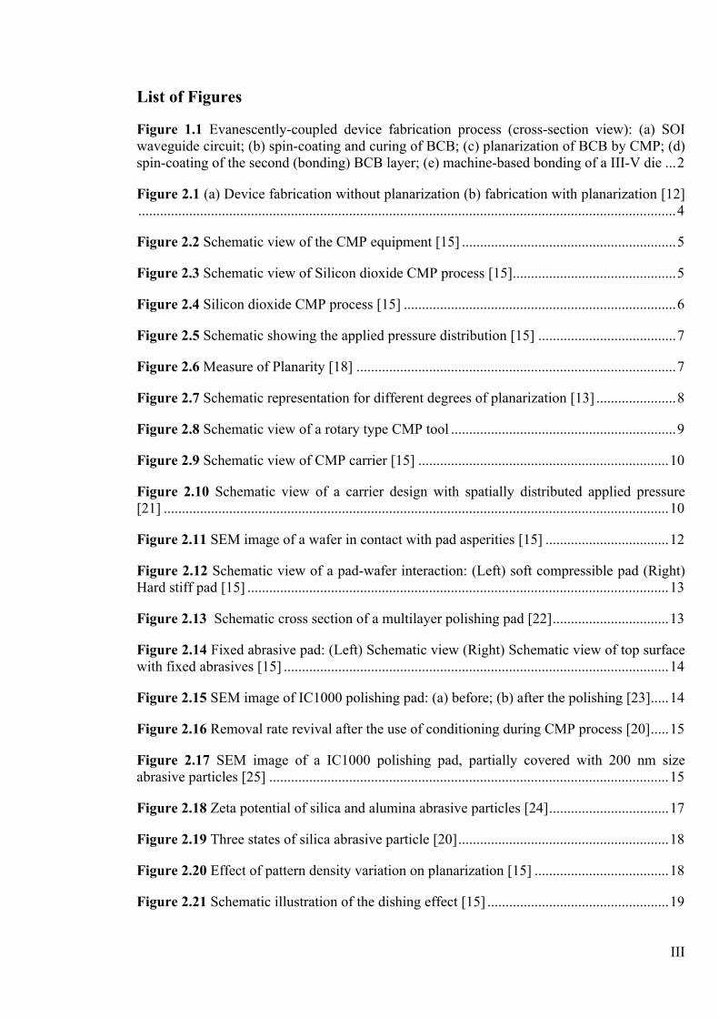
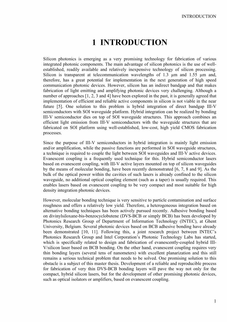
1.1 Aim of the Project The final goal of this project is to demonstrate an active photonic device fabricated in SOI/III-V material system using BCB adhesive bonding process, where evanescent coupling technique is used to couple the light from SOI waveguide circuits into the III-V active layers. The fabrication process is schematically presented in Figure 1.1.
Figure 1.1 Evanescently-coupled device fabrication process (cross-section view): (a) SOI waveguide circuit; (b) spin-coating and curing of BCB; (c) planarization of BCB by CMP; (d) spin-coating of the second (bonding) BCB layer; (e) machine-based bonding of a III-V die
The fabrication process starts with spin-coating and curing of a relatively thick BCB layer. This BCB film will be non-planarized due to the topography of SOI waveguide circuit. BCB will be planarized and thinned down by using a CMP process. Development of a BCB CMP process is the main goal of this project. After planarization and thinning down of BCB film, another very thin BCB film will be spin-coated. This film will act as a bonding layer for the next step of III-V die bonding. After the bonding of a III-V die to an SOI waveguide circuit, a required active photonic device will be fabricated by processing of the bonded III-V die. The active photonic device we chose is a metal-semiconductor-metal (MSM) photo-detector whose design is given in PhD thesis of Joost Brouckaert [11].
In the following chapters, we will present a chemical mechanical planarization (CMP) process development for BCB. Chapter 2 will present the basics of CMP process in general. In

INTRODUCTION
3
Chapter 3, we will deal with BCB properties relevant for CMP process development. Issues related to CMP of BCB, as well as the literature review of BCB CMP will also be presented in this chapter. Chapter 4 will focus on our approach for BCB CMP process development, while in Chapter 5, details of the experiments and the results of this process development will be presented. Fabrication of a MSM photo-detector will be described in Chapter 6. In the end, conclusions and prospects for the future work will be presented.
CMP BASICS
4
2 CMP BASICS
Chemical mechanical planarization (CMP) is a process where mechanical and chemical forces act together to smoothen and planarize a surface. Sometimes CMP is also used for chemical mechanical polishing which involves smoothening of a surface but not necessarily planarization. In this study, we will use CMP in context of planarization rather than polishing.
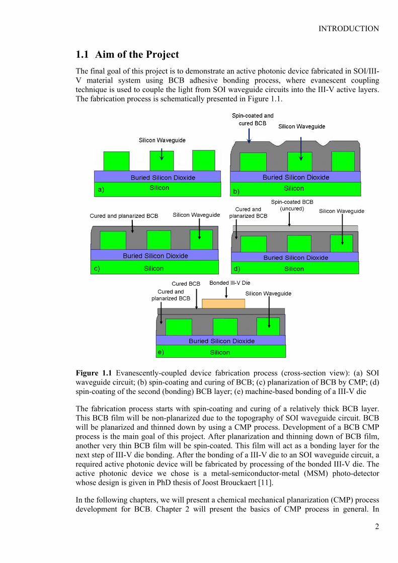
2.1 Why CMP? CMP is a very important and most efficient planarization method. In our case, we need a very planarized surface to improve the yield of our bonding process as discussed in chapter 1. Also, as the device dimensions are scaling down, we need multilevel metallization, but with every additional layer the surface topography gets worsen. As depicted in Figure 2.1, to fabricate small features, we need a minimum depth of focus (DOF) which in turn requires good planarization of the surface.
Figure 2.1 (a) Device fabrication without planarization (b) fabrication with planarization [12]
A number of techniques are available for planarization: e.g. spin on deposition, etch back and reflow of boron phosphorous silicate glass. These techniques can offer local planarization (on the order of microns) but they cannot provide global planarization (on the order of millimeters). Only CMP can provide planarization at both local and global levels [13, 14].
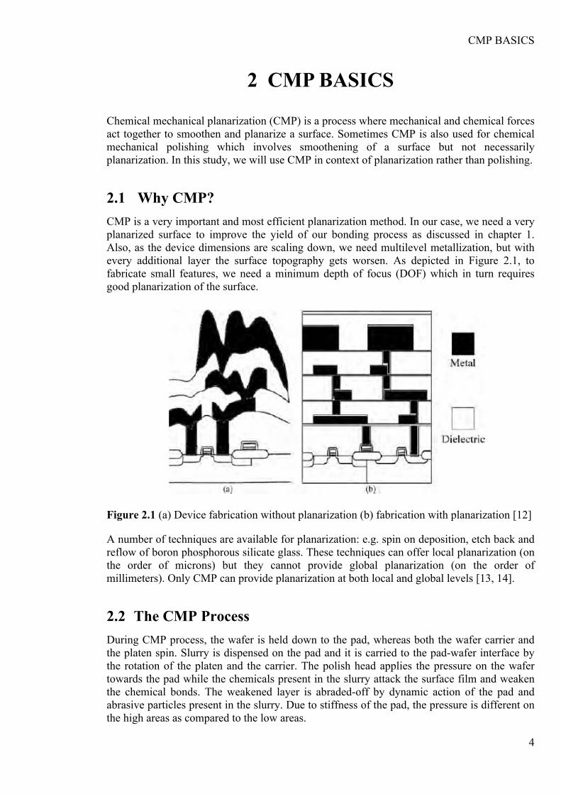
2.2 The CMP Process During CMP process, the wafer is held down to the pad, whereas both the wafer carrier and the platen spin. Slurry is dispensed on the pad and it is carried to the pad-wafer interface by the rotation of the platen and the carrier. The polish head applies the pressure on the wafer towards the pad while the chemicals present in the slurry attack the surface film and weaken the chemical bonds. The weakened layer is abraded-off by dynamic action of the pad and abrasive particles present in the slurry. Due to stiffness of the pad, the pressure is different on the high areas as compared to the low areas.
CMP BASICS
5
Consequently, a different amount of material is removed in these areas and, as a result of this, planarization of the surface improves. This process continues until desired amount of material is removed. During this process, a diamond conditioner maintains the surface roughness of the pad to ensure repeatability of the CMP process. A schematic view of CMP equipment is shown in Figure 2.2.
Figure 2.2 Schematic view of the CMP equipment [15]
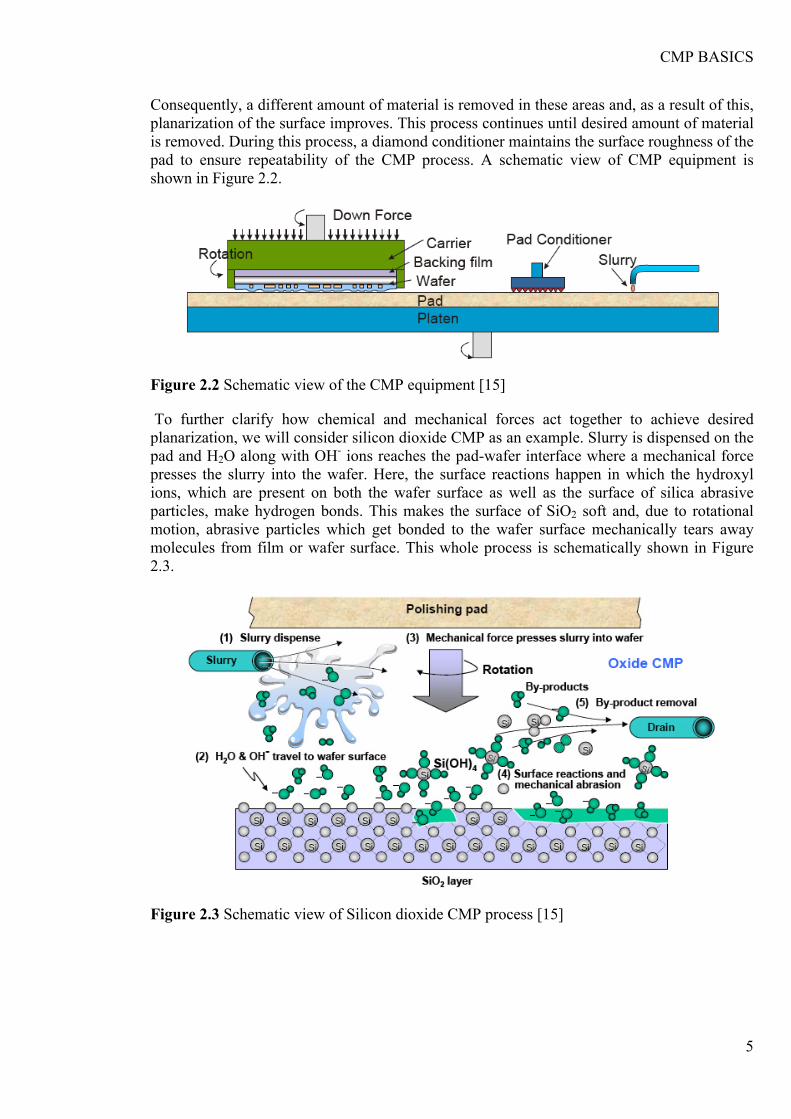
To further clarify how chemical and mechanical forces act together to achieve desired planarization, we will consider silicon dioxide CMP as an example. Slurry is dispensed on the pad and H2O along with OH- ions reaches the pad-wafer interface where a mechanical force presses the slurry into the wafer. Here, the surface reactions happen in which the hydroxyl ions, which are present on both the wafer surface as well as the surface of silica abrasive particles, make hydrogen bonds. This makes the surface of SiO2 soft and, due to rotational motion, abrasive particles which get bonded to the wafer surface mechanically tears away molecules from film or wafer surface. This whole process is schematically shown in Figure 2.3.
Figure 2.3 Schematic view of Silicon dioxide CMP process [15]
CMP BASICS
6
2.2.1 Preston’s Model One important output variable of a CMP process is the amount of material being removed in a given time. This is called material removal rate (MRR). The most frequent and also the very first model to predict the MRR is Preston’s equation [16] given below:
ΔH VMRR= = Kp P Δt t
ΔΔ
where ΔH is the change in height of the surface, Δt is the elapsed time, Kp is Preston coefficient, P is the applied pressure and ΔV/ Δt is the velocity of pad rotation relative to wafer. This relation shows that the MRR is directly proportional to both applied pressure and relative velocity and it is essentially zero in absence of any of them. The effect of slurry pad and other process parameters is lumped into Preston coefficient. Considering only mechanical properties of hard materials like silicon or silicon dioxide, Brown et al. [17] approximated this coefficient as
1Kp=2Ey
where Ey is the Young’s modulus of the material being polished.
It should be noted here that Preston’s model considers only the material removal mechanically, so it’s not an accurate model, but a very simple and straightforward model which can be used to roughly predict MRR with a given set of process parameters. Figure 2.4 shows an example of a silicon dioxide CMP process with representative numbers for MRR, the applied pressure and the relative velocity.
Figure 2.4 Silicon dioxide CMP process [15]

CMP BASICS
7
2.2.2 Planarization As we see from Preston’s model, MRR is directly proportional to the applied pressure P. We also know that P = F / A, where F is the applied force and A is the contact area between the wafer and the pad, which might not be the geometric area of the wafer as shown in Figure 2.5.
Figure 2.5 Schematic showing the applied pressure distribution [15]
If the wafer surface has some topography, then the contact area will be less than the geometric area. So, planarization occurs because the material is removed only from the high areas. When the surface gets smoothen, then the contact area becomes equal to geometric area and thus removal rate decreases and the surface is planarized. However, this is an ideal case where the pad only touches the high (protruding) areas. In reality, the pad conforms to a certain extent to the topography of the surface and we also get some material removed in the low areas. However, because of the applied pressure difference in the low and the high areas, the removal rate will be different in these areas and so we can still get planarization, though it cannot be perfectly flat now.
Several different methods can be used to measure the degree of planarization. Figure 2.6 shows a very basic measure of planarity.
Figure 2.6 Measure of Planarity [18]
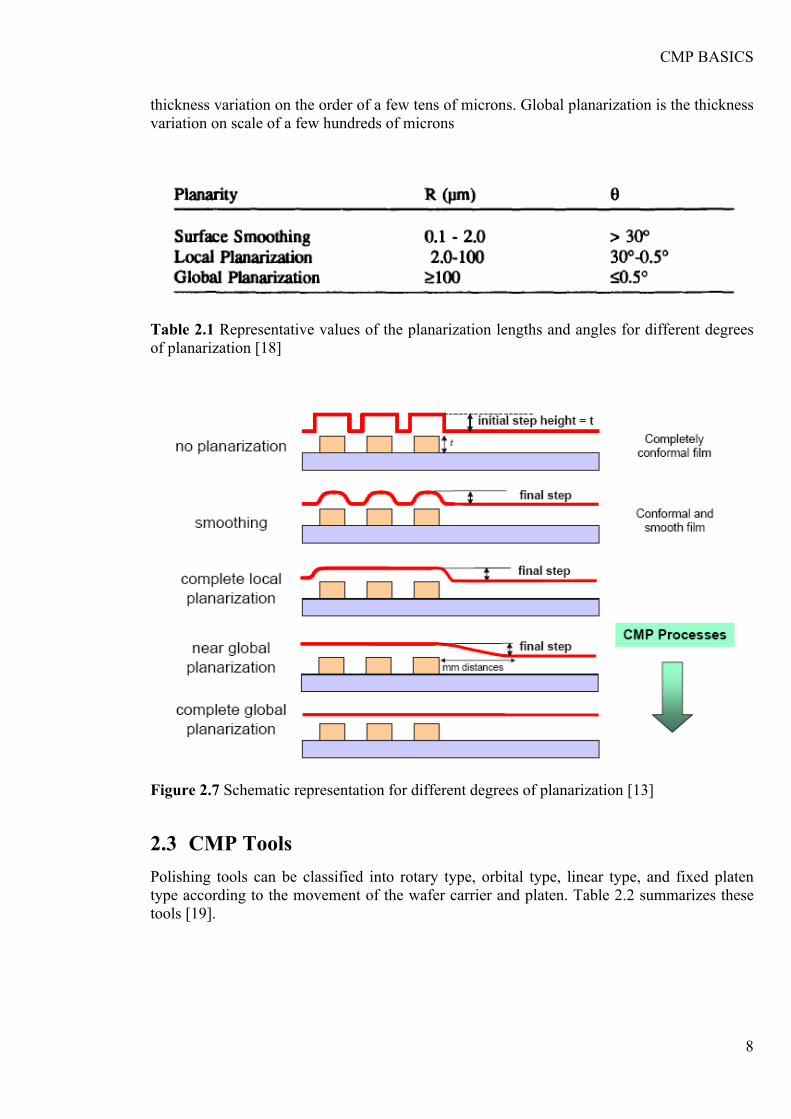
The planarization length is defined as "The distance, R, traveled over a step, where upon the original step height, topography, or depth of field, T, returns” [18]. The planarization angle is given by θ = arctan(T/R). Values of planarization lengths and angles for surface smoothing, local planarization, and global planarization are given in Table 2.1 [18]. Schematic representation of the degree of planarization is given in Figure 2.7 [13]. Surface smoothing is a very small scale and high spatial frequency variation of thickness. Local planarization is the
CMP BASICS
8
thickness variation on the order of a few tens of microns. Global planarization is the thickness variation on scale of a few hundreds of microns
Table 2.1 Representative values of the planarization lengths and angles for different degrees of planarization [18]
Figure 2.7 Schematic representation for different degrees of planarization [13]
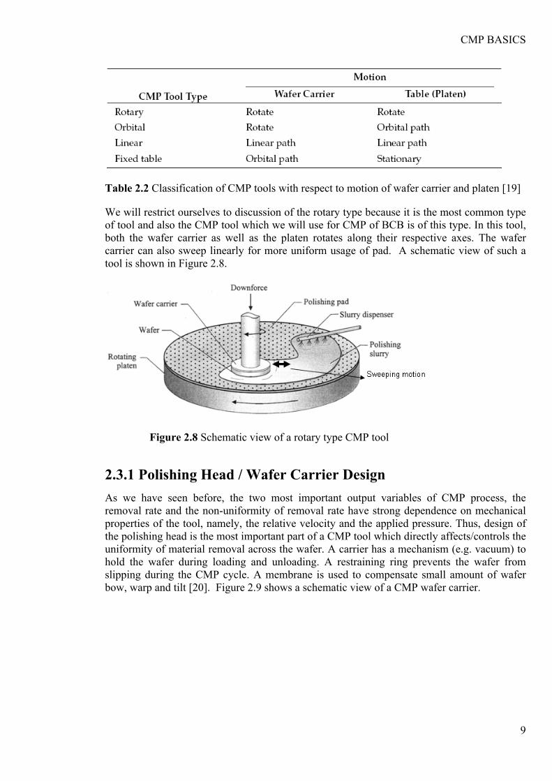
2.3 CMP Tools Polishing tools can be classified into rotary type, orbital type, linear type, and fixed platen type according to the movement of the wafer carrier and platen. Table 2.2 summarizes these tools [19].
CMP BASICS
9
Table 2.2 Classification of CMP tools with respect to motion of wafer carrier and platen [19]
We will restrict ourselves to discussion of the rotary type because it is the most common type of tool and also the CMP tool which we will use for CMP of BCB is of this type. In this tool, both the wafer carrier as well as the platen rotates along their respective axes. The wafer carrier can also sweep linearly for more uniform usage of pad. A schematic view of such a tool is shown in Figure 2.8.
Figure 2.8 Schematic view of a rotary type CMP tool
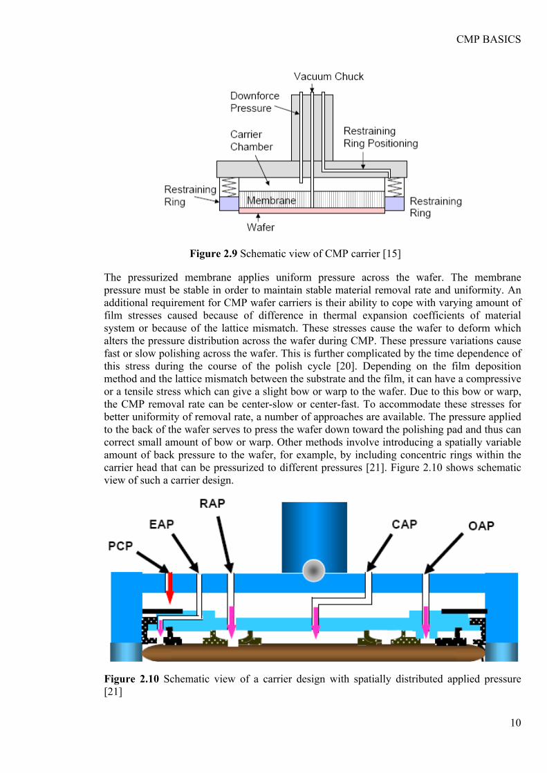
2.3.1 Polishing Head / Wafer Carrier Design As we have seen before, the two most important output variables of CMP process, the removal rate and the non-uniformity of removal rate have strong dependence on mechanical properties of the tool, namely, the relative velocity and the applied pressure. Thus, design of the polishing head is the most important part of a CMP tool which directly affects/controls the uniformity of material removal across the wafer. A carrier has a mechanism (e.g. vacuum) to hold the wafer during loading and unloading. A restraining ring prevents the wafer from slipping during the CMP cycle. A membrane is used to compensate small amount of wafer bow, warp and tilt [20]. Figure 2.9 shows a schematic view of a CMP wafer carrier.
CMP BASICS
10
Figure 2.9 Schematic view of CMP carrier [15]
The pressurized membrane applies uniform pressure across the wafer. The membrane pressure must be stable in order to maintain stable material removal rate and uniformity. An additional requirement for CMP wafer carriers is their ability to cope with varying amount of film stresses caused because of difference in thermal expansion coefficients of material system or because of the lattice mismatch. These stresses cause the wafer to deform which alters the pressure distribution across the wafer during CMP. These pressure variations cause fast or slow polishing across the wafer. This is further complicated by the time dependence of this stress during the course of the polish cycle [20]. Depending on the film deposition method and the lattice mismatch between the substrate and the film, it can have a compressive or a tensile stress which can give a slight bow or warp to the wafer. Due to this bow or warp, the CMP removal rate can be center-slow or center-fast. To accommodate these stresses for better uniformity of removal rate, a number of approaches are available. The pressure applied to the back of the wafer serves to press the wafer down toward the polishing pad and thus can correct small amount of bow or warp. Other methods involve introducing a spatially variable amount of back pressure to the wafer, for example, by including concentric rings within the carrier head that can be pressurized to different pressures [21]. Figure 2.10 shows schematic view of such a carrier design.
Figure 2.10 Schematic view of a carrier design with spatially distributed applied pressure [21]
CMP BASICS
11
Carrier has four zones to control uniformity through varying air pressures. The Polishing Chamber Pressure (PCP) is used to adjust the overall polishing pressure of the head which is normally held constant during polishing cycle. Other pressures are varied to control the uniformity during the polishing cycle.
CAP: Center Air Pressure (0mm - 30mm)
RAP: Ripple Air Pressure (31mm - 64mm)
OAP: Outer Air Pressure (65mm - 84mm)
EAP: Edge Air Pressure (85mm – 100mm)
A number of other more advanced and sophisticated carrier designs, like gimbaled carriers and floating carriers, also exist, but their discussion is beyond the scope of this thesis.
2.4 CMP Consumables CMP is a highly consumable-driven process. The most important consumables for this process are pad, diamond conditioner/dresser and slurry. In this section, we will discuss details about these consumables and how they affect the output variables, i.e. surface roughness, removal rate and non-uniformity of a CMP process.
2.4.1 Polishing Pads In a very simplistic view, CMP can be seen as rubbing of a wafer against some flat surface and, with the help of fine particles in a water-based solution, removing material in the protruding areas to get the desired planarization. The flat surface during the process and the medium for the frictional force to act upon the wafer, is provided by the polishing pad. The polishing pads used in semiconductor industry can be categorized in four main types with respect to their structural characteristics. These are given as below [22, 23]
Type I: Felts and polymer-impregnated felts
Type II: Porometrics (microporous synthetic leathers)
Type III: Filled polymer sheets (films)
Type IV: Unfilled textured polymer sheets (films)
Table 2.3 summarizes different physical and mechanical properties of these types [13, 22].
Polishing pad has an effect on all the output variables of a CMP process (surface roughness, material removal, non-uniformity) as it interacts with all the input variables (pressure, velocity, slurry abrasive). Pad fibers extending from the surface are called asperities and they interact with the wafer surface. Their height affects the slurry transport and local pressure gradients. The pad top surface contains micropores which help in slurry transport to the wafer and taking away the reaction byproducts. A large pore size is desirable, but the size of pores will also affect the mechanical properties of the pad by changing the average thickness of pad. Figure 2.11 shows the relative size of pad asperities, pores and circuit features on the wafer.

CMP BASICS
12
Table 2.3 Summary of different pad properties [13, 22]
Figure 2.11 SEM image of a wafer in contact with pad asperities [15]
Pad compressibility affects the pad conformability to the wafer surface. Ideally, the pad should not contact the low regions and thus should not be conformal. Hence, low compressibility is desirable for a good planarization. However, to obtain good uniformity in removal rate across the wafer, the pad must contact uniformly across the wafer and therefore must be conformal on a long-range scale. To balance between planarity and uniformity, a
CMP BASICS
13
two-pad system is usually used. A hard top pad provides good planarity, while a more compressible bottom pad provides long-range conformability and thus better uniformity.
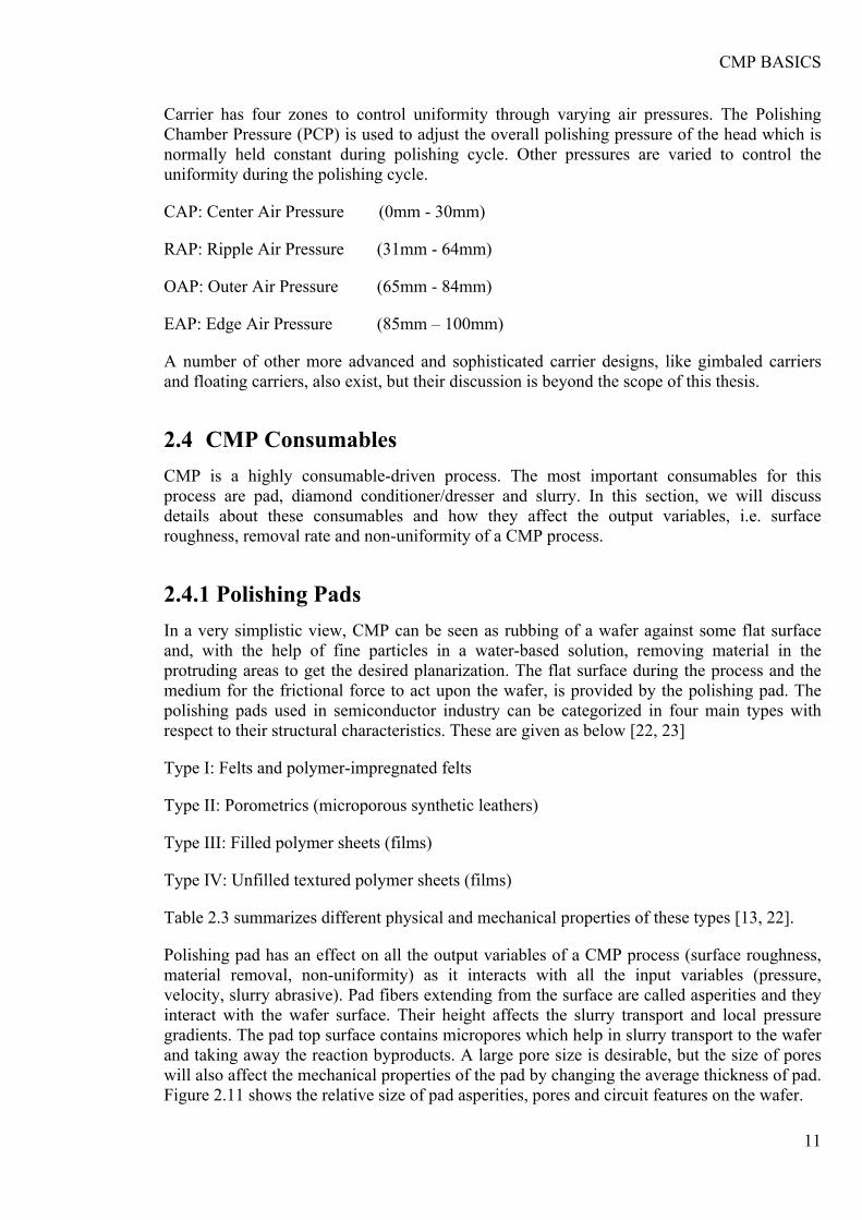
Pad hardness affects the planarization. Harder pads provide better planarity, while softer pads provide defect-free surfaces [13]. Figure 2.12 shows schematically how a hard, less compressible pad can provide better planarization, while a soft, compressible pad gives a poor planarization.
Figure 2.12 Schematic view of a pad-wafer interaction: (Left) soft compressible pad (Right) Hard stiff pad [15]
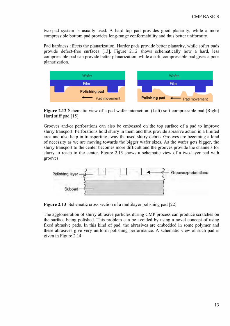
Grooves and/or perforations can also be embossed on the top surface of a pad to improve slurry transport. Perforations hold slurry in them and thus provide abrasive action in a limited area and also help in transporting away the used slurry debris. Grooves are becoming a kind of necessity as we are moving towards the bigger wafer sizes. As the wafer gets bigger, the slurry transport to the center becomes more difficult and the grooves provide the channels for slurry to reach to the center. Figure 2.13 shows a schematic view of a two-layer pad with grooves.
Figure 2.13 Schematic cross section of a multilayer polishing pad [22]
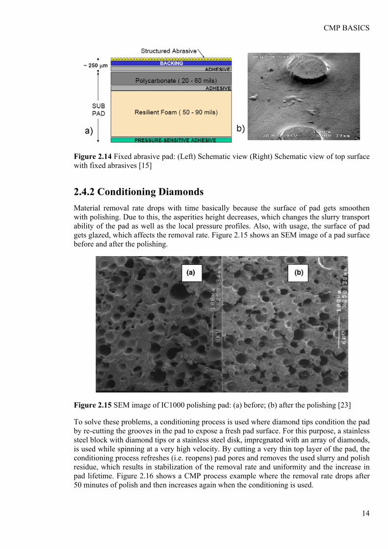
The agglomeration of slurry abrasive particles during CMP process can produce scratches on the surface being polished. This problem can be avoided by using a novel concept of using fixed abrasive pads. In this kind of pad, the abrasives are embedded in some polymer and these abrasives give very uniform polishing performance. A schematic view of such pad is given in Figure 2.14.
CMP BASICS
14
Figure 2.14 Fixed abrasive pad: (Left) Schematic view (Right) Schematic view of top surface with fixed abrasives [15]
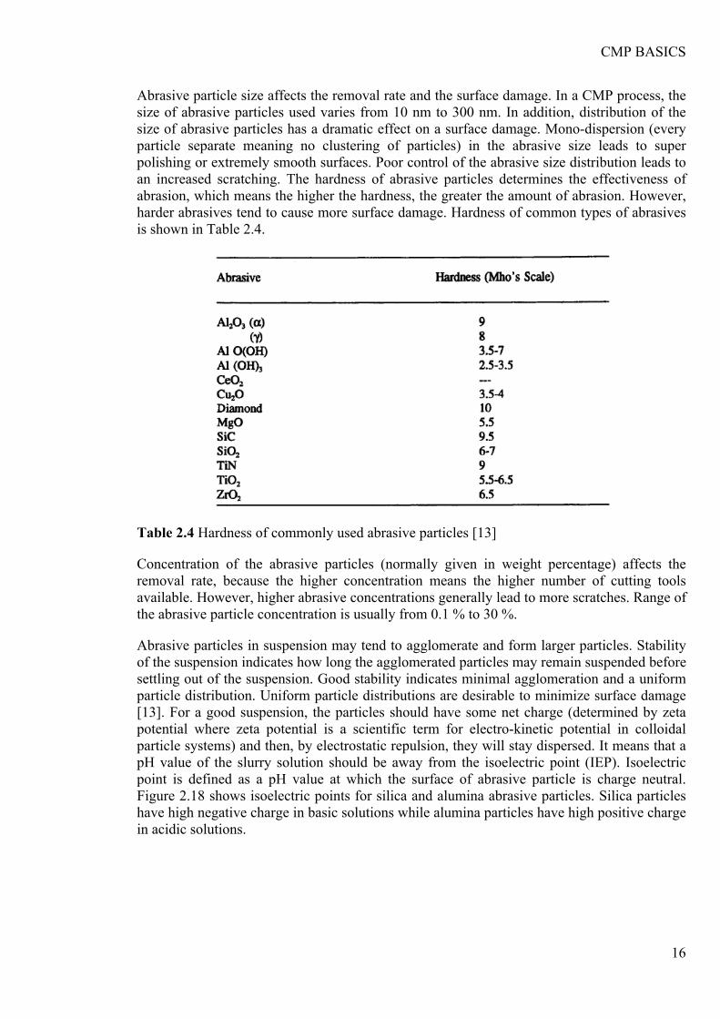
2.4.2 Conditioning Diamonds Material removal rate drops with time basically because the surface of pad gets smoothen with polishing. Due to this, the asperities height decreases, which changes the slurry transport ability of the pad as well as the local pressure profiles. Also, with usage, the surface of pad gets glazed, which affects the removal rate. Figure 2.15 shows an SEM image of a pad surface before and after the polishing.
Figure 2.15 SEM image of IC1000 polishing pad: (a) before; (b) after the polishing [23]
To solve these problems, a conditioning process is used where diamond tips condition the pad by re-cutting the grooves in the pad to expose a fresh pad surface. For this purpose, a stainless steel block with diamond tips or a stainless steel disk, impregnated with an array of diamonds, is used while spinning at a very high velocity. By cutting a very thin top layer of the pad, the conditioning process refreshes (i.e. reopens) pad pores and removes the used slurry and polish residue, which results in stabilization of the removal rate and uniformity and the increase in pad lifetime. Figure 2.16 shows a CMP process example where the removal rate drops after 50 minutes of polish and then increases again when the conditioning is used.

CMP BASICS
15
Figure 2.16 Removal rate revival after the use of conditioning during CMP process [20]
2.4.3 Slurry The choice of slurry used in CMP process is directly linked to the material which is being polished. This means that a slurry, which is, for example, developed for silicon dioxide CMP might not give satisfactory results for copper CMP and vice versa. This is because the slurry chemical reactions are different for the different materials.
Basically, slurry consists of two components: the abrasive particles and the solution. Type of the abrasives, the chemicals used and the synergy among them defines behavior of the slurry for different materials that are being polished.
2.4.3.1 Abrasive particles
The slurry abrasive provides the mechanical action of CMP. Size, type and concentration of the slurry abrasive have a different effect on mechanical abrasion. Silica (SiO2) and alumina (Al2O3) are most often used as abrasive particles. Ceria (CeO2), titania (TiO2), magnesium oxide (MgO) and zirconia (ZrO2) are also used in different applications. Figure 2.17 shows a SEM image of silica abrasive particles.
Figure 2.17 SEM image of a IC1000 polishing pad, partially covered with 200 nm size abrasive particles [25]
CMP BASICS
16
Abrasive particle size affects the removal rate and the surface damage. In a CMP process, the size of abrasive particles used varies from 10 nm to 300 nm. In addition, distribution of the size of abrasive particles has a dramatic effect on a surface damage. Mono-dispersion (every particle separate meaning no clustering of particles) in the abrasive size leads to super polishing or extremely smooth surfaces. Poor control of the abrasive size distribution leads to an increased scratching. The hardness of abrasive particles determines the effectiveness of abrasion, which means the higher the hardness, the greater the amount of abrasion. However, harder abrasives tend to cause more surface damage. Hardness of common types of abrasives is shown in Table 2.4.
Table 2.4 Hardness of commonly used abrasive particles [13]
Concentration of the abrasive particles (normally given in weight percentage) affects the removal rate, because the higher concentration means the higher number of cutting tools available. However, higher abrasive concentrations generally lead to more scratches. Range of the abrasive particle concentration is usually from 0.1 % to 30 %.
Abrasive particles in suspension may tend to agglomerate and form larger particles. Stability of the suspension indicates how long the agglomerated particles may remain suspended before settling out of the suspension. Good stability indicates minimal agglomeration and a uniform particle distribution. Uniform particle distributions are desirable to minimize surface damage [13]. For a good suspension, the particles should have some net charge (determined by zeta potential where zeta potential is a scientific term for electro-kinetic potential in colloidal particle systems) and then, by electrostatic repulsion, they will stay dispersed. It means that a pH value of the slurry solution should be away from the isoelectric point (IEP). Isoelectric point is defined as a pH value at which the surface of abrasive particle is charge neutral. Figure 2.18 shows isoelectric points for silica and alumina abrasive particles. Silica particles have high negative charge in basic solutions while alumina particles have high positive charge in acidic solutions.
CMP BASICS
17
Figure 2.18 Zeta potential of silica and alumina abrasive particles [24]
2.4.3.2 Slurry Solution
Slurry solution includes water as well as other chemical components, except the abrasive particles. In the first place, as shown in Figure 2.18, the pH value of the slurry solution should be adjusted to some value well away from the isoelectric point in order to have a good electrostatic suspension of the abrasive particles. For example, when silica abrasive particles are used, pH is then adjusted to around 10 (basic solution), while for alumina particles, pH is adjusted to around 3 (acidic solution). Each material being polished has a different chemistry, as far as the chemical interactions with the slurry are concerned. Slurry chemicals affect primarily the chemical component of CMP process, e.g., etch rate. However, chemical reactions modify the mechanical properties of the film, the pad, and the abrasive surfaces, which, as a result, affect the mechanical component of CMP process. The pH value also affects the dissolution rate and the solubility of the material being abraded. Thus, a good control of the pH value is very important. Buffering agents are used to keep the pH value constant throughout the slurry volume and over the time. Without buffering agents, the pH may be dramatically different at the wafer surface if surface reactions consume or produce H+ ions. For metal CMP, most of the chemical reactions are electrochemical in nature. Oxidizers react with metal surfaces to raise the oxidation state of the metal via a reduction-oxidation reaction, resulting in either dissolution of the metal or the formation of a surface film on the metal. Surfactants increase the solubility of the film being polished or the abraded film material. Surfactants can also change the isolectric point, as shown in Figure 2.18 with the green dotted curve [24].
2.5 CMP Process Issues A number of CMP process issues can occur and some of them are common to any CMP process while few of them depend on the material being polished and the changes in topography of the wafer. Scratches, remaining slurry abrasive particles and surface residues are common to any CMP application. Removal of the remaining particles as well as the surface residues will be discussed in the next section.
CMP BASICS
18
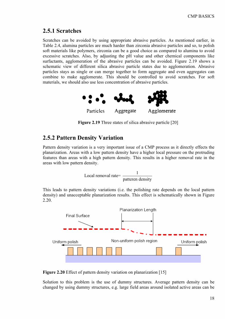
2.5.1 Scratches Scratches can be avoided by using appropriate abrasive particles. As mentioned earlier, in Table 2.4, alumina particles are much harder than zirconia abrasive particles and so, to polish soft materials like polymers, zirconia can be a good choice as compared to alumina to avoid excessive scratches. Also, by adjusting the pH value and other chemical components like surfactants, agglomeration of the abrasive particles can be avoided. Figure 2.19 shows a schematic view of different silica abrasive particle states due to agglomeration. Abrasive particles stays as single or can merge together to form aggregate and even aggregates can combine to make agglomerate. This should be controlled to avoid scratches. For soft materials, we should also use less concentration of abrasive particles.
Figure 2.19 Three states of silica abrasive particle [20]
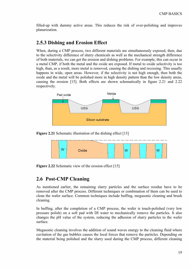
2.5.2 Pattern Density Variation Pattern density variation is a very important issue of a CMP process as it directly effects the planarization. Areas with a low pattern density have a higher local pressure on the protruding features than areas with a high pattern density. This results in a higher removal rate in the areas with low pattern density.
1Local removal rate= patteren density
This leads to pattern density variations (i.e. the polishing rate depends on the local pattern density) and unacceptable planarization results. This effect is schematically shown in Figure 2.20.
Figure 2.20 Effect of pattern density variation on planarization [15]
Solution to this problem is the use of dummy structures. Average pattern density can be changed by using dummy structures, e.g. large field areas around isolated active areas can be
CMP BASICS
19
filled-up with dummy active areas. This reduces the risk of over-polishing and improves planarization.
2.5.3 Dishing and Erosion Effect When, during a CMP process, two different materials are simultaneously exposed, then, due to the selectivity difference of slurry chemicals as well as the mechanical strength difference of both materials, we can get the erosion and dishing problems. For example, this can occur in a metal CMP, if both the metal and the oxide are exposed. If metal to oxide selectivity is too high, than, as a result, more metal is removed, causing the dishing and recessing. This usually happens in wide, open areas. However, if the selectivity is not high enough, then both the oxide and the metal will be polished more in high density pattern than the low density areas, causing the erosion [15]. Both effects are shown schematically in figure 2.21 and 2.22 respectively.
Figure 2.21 Schematic illustration of the dishing effect [15]
Figure 2.22 Schematic view of the erosion effect [15]
2.6 Post-CMP Cleaning As mentioned earlier, the remaining slurry particles and the surface residue have to be removed after the CMP process. Different techniques or combination of them can be used to clean the wafer surface. Common techniques include buffing, megasonic cleaning and brush cleaning.
In buffing, after the completion of a CMP process, the wafer is touch-polished (very low pressure polish) on a soft pad with DI water to mechanically remove the particles. It also changes the pH value of the system, reducing the adhesion of slurry particles to the wafer surface.
Megasonic cleaning involves the addition of sound waves energy to the cleaning fluid where cavitation of the gas bubbles causes the local forces that remove the particles. Depending on the material being polished and the slurry used during the CMP process, different cleaning
CMP BASICS
20
chemicals like TMAH (tri-methyl ammonium hydroxide), SC-1 (standard cleaning solution 1), etc. can be added.
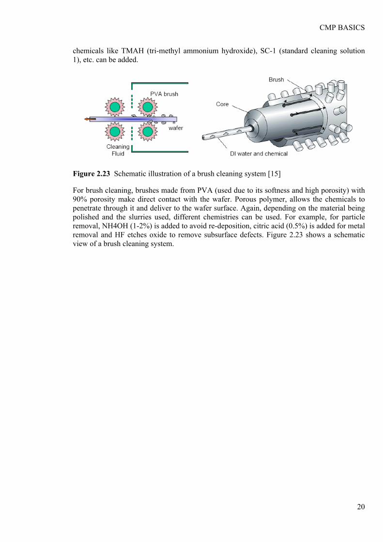
Figure 2.23 Schematic illustration of a brush cleaning system [15]
For brush cleaning, brushes made from PVA (used due to its softness and high porosity) with 90% porosity make direct contact with the wafer. Porous polymer, allows the chemicals to penetrate through it and deliver to the wafer surface. Again, depending on the material being polished and the slurries used, different chemistries can be used. For example, for particle removal, NH4OH (1-2%) is added to avoid re-deposition, citric acid (0.5%) is added for metal removal and HF etches oxide to remove subsurface defects. Figure 2.23 shows a schematic view of a brush cleaning system.
BCB CMP PROCESS
21
3 BCB CMP PROCESS
In this chapter, we will discuss the properties of divinylsiloxane-bis-benzocyclobutene (DVS-BCB). Hereafter, for the sake of brevity, this material will be referred to as BCB. We will also discuss the issues related to CMP process development for BCB. In the end, a literature review of BCB CMP processes will be presented.
3.1 BCB Properties BCB is a thermosetting polymer, commonly used in the electronics industry. It is developed by Dow Chemicals Company with a commercial name of Cyclotene®. It is available in dry etch and photo-definable grades, commercially known as 3000 series and 4000 series resins, respectively. In photonics applications, we work with a dry etch Cyclotene 3022-35 resin, so we will focus exclusively to this type of BCB.
3.1.1 Chemical structure BCB is a well-known material in CMOS industry, as it has been used as an inter-layer dielectric (ILD) in CMOS metallization stacks [26]. BCB monomer is a symmetrical molecule, containing silicon in its backbone, terminated by two benzocyclobutene rings. This monomer can be B-staged, meaning it can be partially cured to form an oligomer. Mesitylene (1,3,5-trimethylbenzene) is used as a solvent to make oligomer solution. When cured, the benzocyclobutene ring thermally opens to form o-quinodimethane. Very reactive intermediate o-quinodimethane readily undergoes a so called Diels-Alder reaction with an available vinylsiloxane group, to form a three-dimensional network structure as is shown in figure 3.1 [27, 28, and 10]. This reaction mechanism shows that no by-products are created during the polymerization.
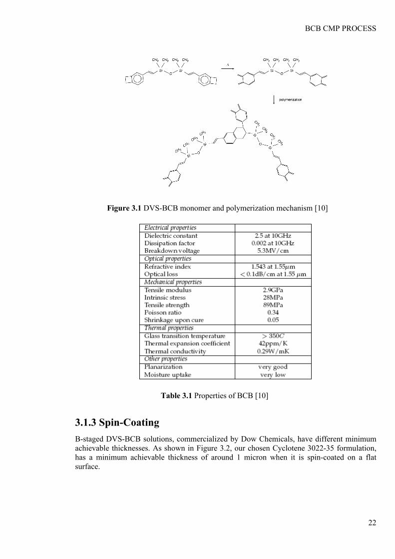
3.1.2 Properties The mechanical, thermal, electrical and optical properties of BCB [27, 29] are presented in Table 3.1 [10]. The most important for our CMP process development is a low shrinkage upon cure, which gives a good pre-CMP planarization. Other interesting properties are the low optical loss at telecommunication wavelengths of 1.3 µm and 1.5 µm and its high glass transition temperature which will provide a large thermal budget for post-CMP processing. However, its tensile modulus is not excellent from a CMP point of view. Tensile modulus is a measure of hardness and mechanical strength of a material and a value of 2.9 GPa means that a BCB film is very soft. For comparison, tensile modulus of silicon dioxide is around 70-90 GPa.
BCB CMP PROCESS
22
Figure 3.1 DVS-BCB monomer and polymerization mechanism [10]
Table 3.1 Properties of BCB [10]
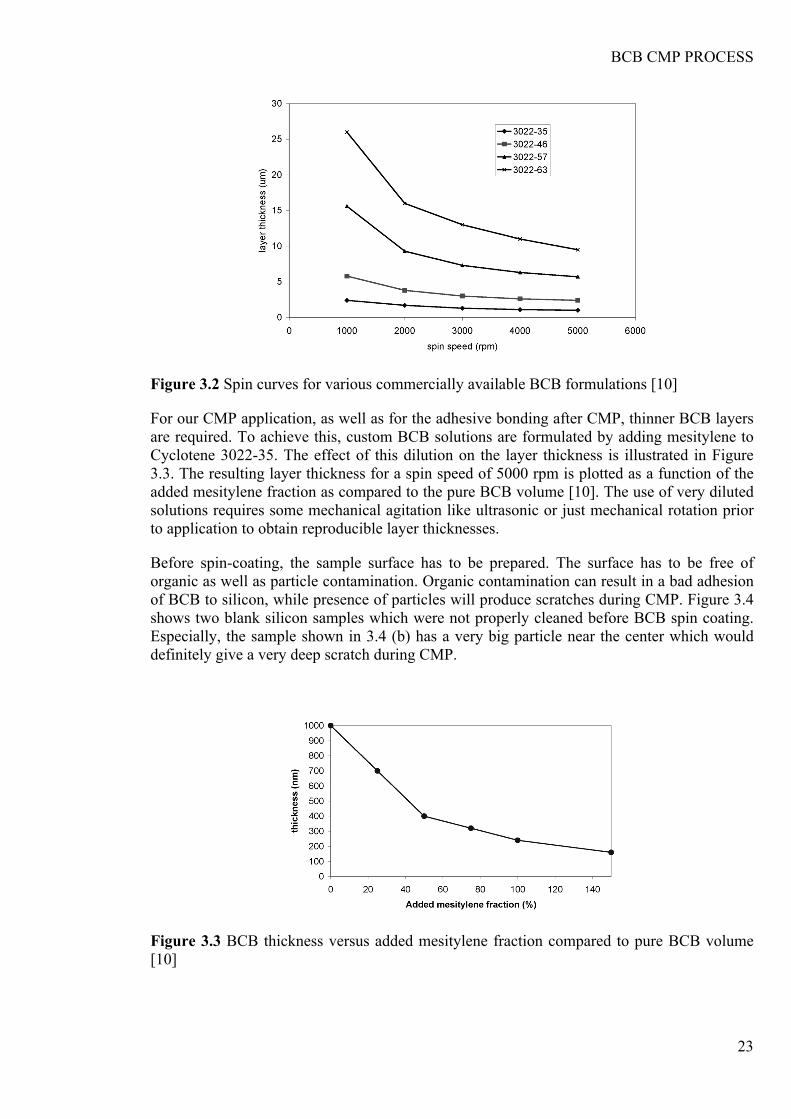
3.1.3 Spin-Coating B-staged DVS-BCB solutions, commercialized by Dow Chemicals, have different minimum achievable thicknesses. As shown in Figure 3.2, our chosen Cyclotene 3022-35 formulation, has a minimum achievable thickness of around 1 micron when it is spin-coated on a flat surface.
BCB CMP PROCESS
23
Figure 3.2 Spin curves for various commercially available BCB formulations [10]
For our CMP application, as well as for the adhesive bonding after CMP, thinner BCB layers are required. To achieve this, custom BCB solutions are formulated by adding mesitylene to Cyclotene 3022-35. The effect of this dilution on the layer thickness is illustrated in Figure 3.3. The resulting layer thickness for a spin speed of 5000 rpm is plotted as a function of the added mesitylene fraction as compared to the pure BCB volume [10]. The use of very diluted solutions requires some mechanical agitation like ultrasonic or just mechanical rotation prior to application to obtain reproducible layer thicknesses.
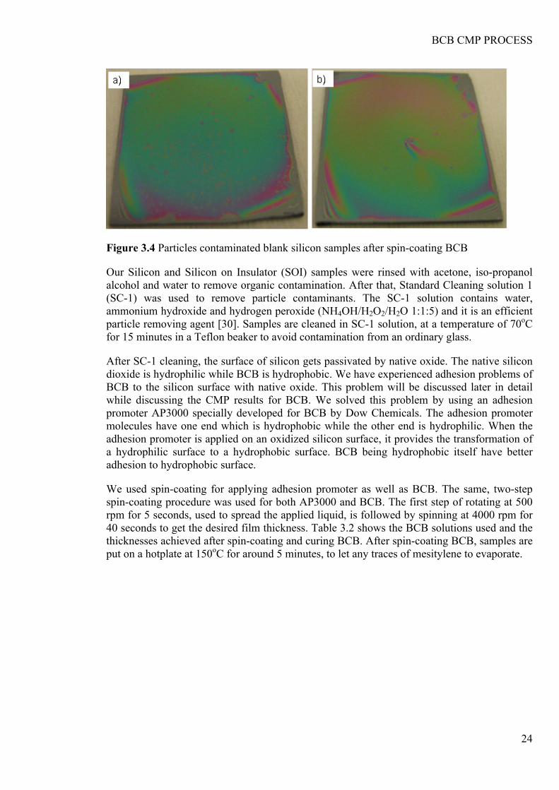
Before spin-coating, the sample surface has to be prepared. The surface has to be free of organic as well as particle contamination. Organic contamination can result in a bad adhesion of BCB to silicon, while presence of particles will produce scratches during CMP. Figure 3.4 shows two blank silicon samples which were not properly cleaned before BCB spin coating. Especially, the sample shown in 3.4 (b) has a very big particle near the center which would definitely give a very deep scratch during CMP.
Figure 3.3 BCB thickness versus added mesitylene fraction compared to pure BCB volume [10]
BCB CMP PROCESS
24
Figure 3.4 Particles contaminated blank silicon samples after spin-coating BCB
Our Silicon and Silicon on Insulator (SOI) samples were rinsed with acetone, iso-propanol alcohol and water to remove organic contamination. After that, Standard Cleaning solution 1 (SC-1) was used to remove particle contaminants. The SC-1 solution contains water, ammonium hydroxide and hydrogen peroxide (NH4OH/H2O2/H2O 1:1:5) and it is an efficient particle removing agent [30]. Samples are cleaned in SC-1 solution, at a temperature of 70oC for 15 minutes in a Teflon beaker to avoid contamination from an ordinary glass.
After SC-1 cleaning, the surface of silicon gets passivated by native oxide. The native silicon dioxide is hydrophilic while BCB is hydrophobic. We have experienced adhesion problems of BCB to the silicon surface with native oxide. This problem will be discussed later in detail while discussing the CMP results for BCB. We solved this problem by using an adhesion promoter AP3000 specially developed for BCB by Dow Chemicals. The adhesion promoter molecules have one end which is hydrophobic while the other end is hydrophilic. When the adhesion promoter is applied on an oxidized silicon surface, it provides the transformation of a hydrophilic surface to a hydrophobic surface. BCB being hydrophobic itself have better adhesion to hydrophobic surface.
We used spin-coating for applying adhesion promoter as well as BCB. The same, two-step spin-coating procedure was used for both AP3000 and BCB. The first step of rotating at 500 rpm for 5 seconds, used to spread the applied liquid, is followed by spinning at 4000 rpm for 40 seconds to get the desired film thickness. Table 3.2 shows the BCB solutions used and the thicknesses achieved after spin-coating and curing BCB. After spin-coating BCB, samples are put on a hotplate at 150oC for around 5 minutes, to let any traces of mesitylene to evaporate.
BCB CMP PROCESS
25
Sample type BCB : Mesitylene Thickness (nm)
Blank Silicon Pure BCB 960 +/- 40
Patterned SOI Pure BCB 1040 +/- 50
Patterned SOI 3:1 460 +/- 30
Patterned SOI 3:2 320 +/- 20
Patterned SOI 5:9 160 +/- 20
Table 3.2 BCB film thicknesses after spin-coating and curing
3.1.4 Curing BCB curing procedure consists of three steps. In first step after spin-coating, BCB is baked on hotplate at temperature 80 – 150oC to drive away any solvent residues. In second step BCB is pre-cured at 150oC for 20 minutes. In third and final step BCB is cured at 250oC for 60 minutes.
During curing, DVS-BCB goes through chemical transformations at a rate which depends on the temperature used for curing. This is graphically represented in a time-temperature-transformation isothermal cure diagram, as shown in Figure 3.5. The main features of such a diagram are obtained by measuring the time needed for events to occur during isothermal cure at different temperatures. This is done by monitoring the degree of polymerization [10].
Three cure profiles for BCB are commonly used: a partial-cure process, a soft-cure process and a hard-cure process. The partially-cured BCB has 45% polymerization, while soft-cure process leads to around 75% polymerization and a hard-cure process leads to a degree of polymerization higher than 95%. As shown in Figure 3.5, degree of polymerization determines the physical state of a BCB film. Partially-cured BCB has a 45% degree of polymerization which is sol/gel or rubber state. BCB in this state cannot survive CMP, so we will not consider it further. Degree of polymerization is a measure of BCB film mechanical strength. The higher this value, the higher will be the mechanical strength of the BCB film. It is desirable to have mechanically strong polishing film so that it can withstand mechanical shear stress of CMP process. The minimum degree of polymerization required for successful CMP is around 85 % [32]. The temperature increase ramp, used during the curing, has also a big effect on the cured BCB film quality in terms of defects and the degree of planarization. This effect will be discussed in detail in the following sections.
BCB CMP PROCESS
26
Figure 3.5 Extent of BCB cure (degree of polymerization) as function of temperature and time [31]
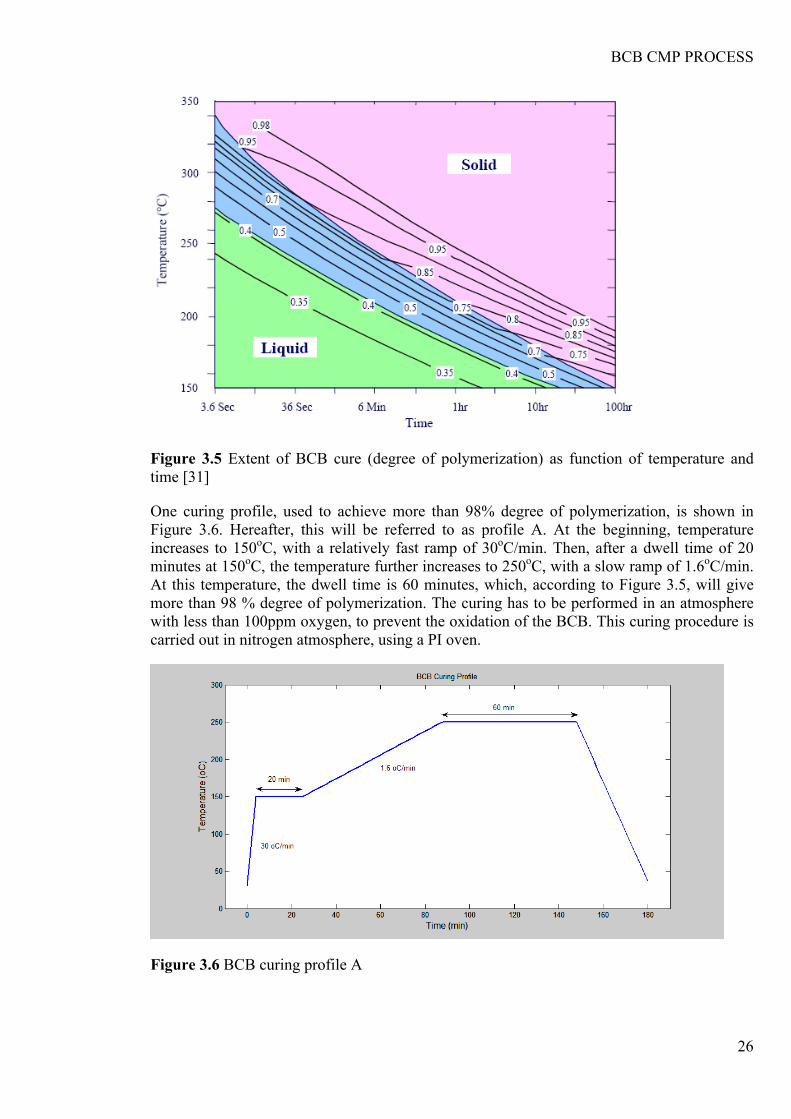
One curing profile, used to achieve more than 98% degree of polymerization, is shown in Figure 3.6. Hereafter, this will be referred to as profile A. At the beginning, temperature increases to 150oC, with a relatively fast ramp of 30oC/min. Then, after a dwell time of 20 minutes at 150oC, the temperature further increases to 250oC, with a slow ramp of 1.6oC/min. At this temperature, the dwell time is 60 minutes, which, according to Figure 3.5, will give more than 98 % degree of polymerization. The curing has to be performed in an atmosphere with less than 100ppm oxygen, to prevent the oxidation of the BCB. This curing procedure is carried out in nitrogen atmosphere, using a PI oven.
Figure 3.6 BCB curing profile A
BCB CMP PROCESS
27
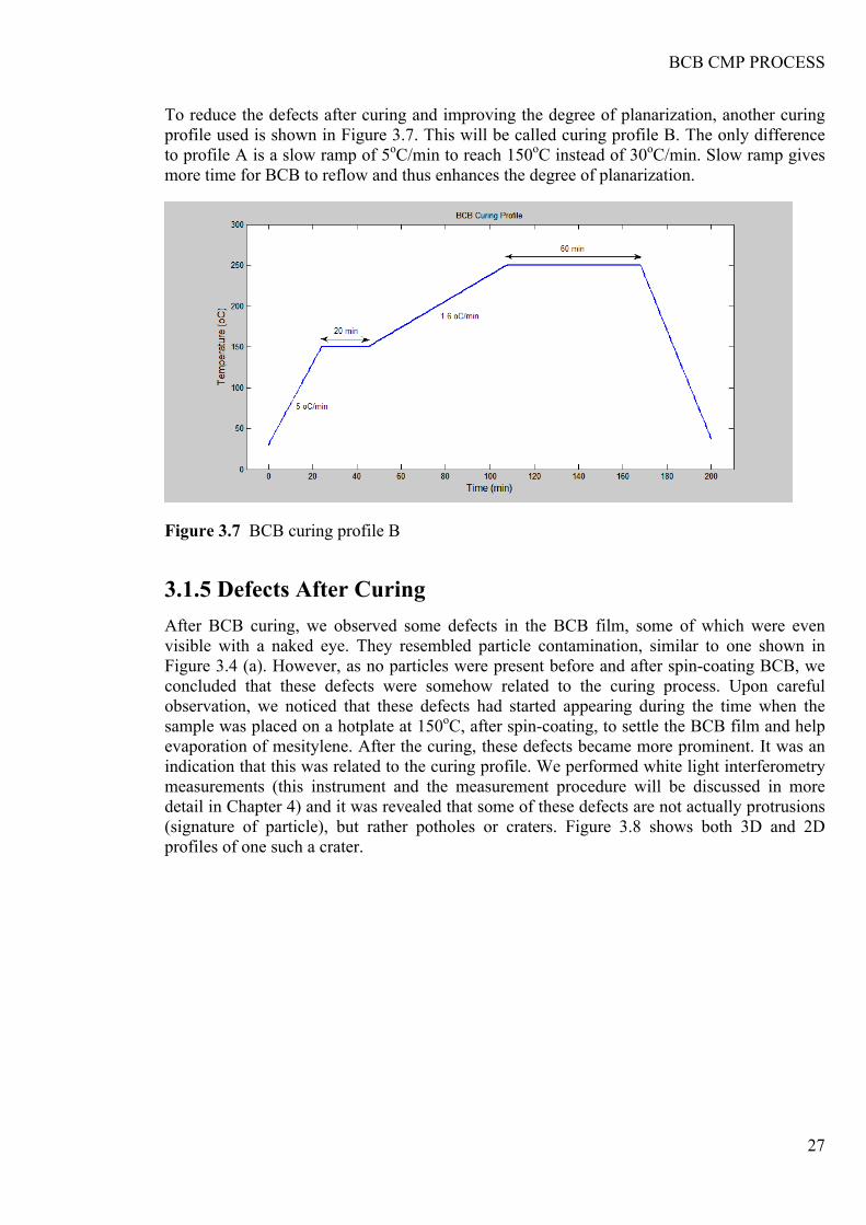
To reduce the defects after curing and improving the degree of planarization, another curing profile used is shown in Figure 3.7. This will be called curing profile B. The only difference to profile A is a slow ramp of 5oC/min to reach 150oC instead of 30oC/min. Slow ramp gives more time for BCB to reflow and thus enhances the degree of planarization.
Figure 3.7 BCB curing profile B
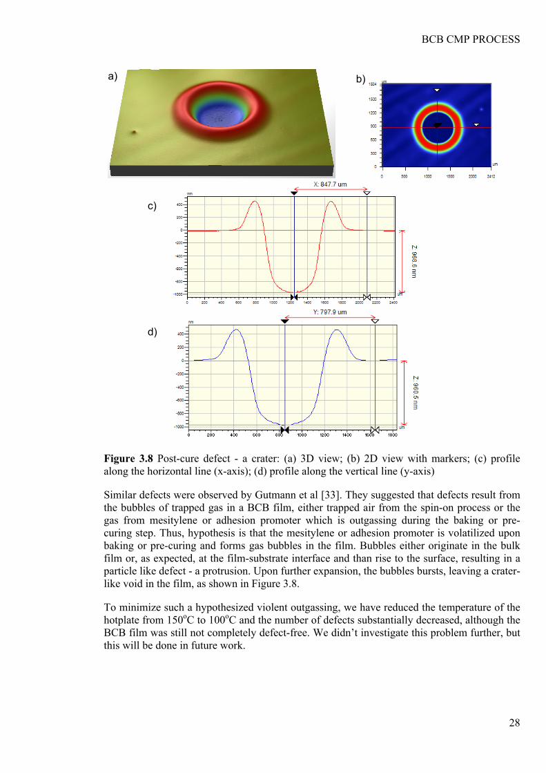
3.1.5 Defects After Curing After BCB curing, we observed some defects in the BCB film, some of which were even visible with a naked eye. They resembled particle contamination, similar to one shown in Figure 3.4 (a). However, as no particles were present before and after spin-coating BCB, we concluded that these defects were somehow related to the curing process. Upon careful observation, we noticed that these defects had started appearing during the time when the sample was placed on a hotplate at 150oC, after spin-coating, to settle the BCB film and help evaporation of mesitylene. After the curing, these defects became more prominent. It was an indication that this was related to the curing profile. We performed white light interferometry measurements (this instrument and the measurement procedure will be discussed in more detail in Chapter 4) and it was revealed that some of these defects are not actually protrusions (signature of particle), but rather potholes or craters. Figure 3.8 shows both 3D and 2D profiles of one such a crater.
BCB CMP PROCESS
28
Figure 3.8 Post-cure defect - a crater: (a) 3D view; (b) 2D view with markers; (c) profile along the horizontal line (x-axis); (d) profile along the vertical line (y-axis)
Similar defects were observed by Gutmann et al [33]. They suggested that defects result from the bubbles of trapped gas in a BCB film, either trapped air from the spin-on process or the gas from mesitylene or adhesion promoter which is outgassing during the baking or pre-curing step. Thus, hypothesis is that the mesitylene or adhesion promoter is volatilized upon baking or pre-curing and forms gas bubbles in the film. Bubbles either originate in the bulk film or, as expected, at the film-substrate interface and than rise to the surface, resulting in a particle like defect - a protrusion. Upon further expansion, the bubbles bursts, leaving a crater-like void in the film, as shown in Figure 3.8.
To minimize such a hypothesized violent outgassing, we have reduced the temperature of the hotplate from 150oC to 100oC and the number of defects substantially decreased, although the BCB film was still not completely defect-free. We didn’t investigate this problem further, but this will be done in future work.
a) b)
c)
d)
BCB CMP PROCESS
29
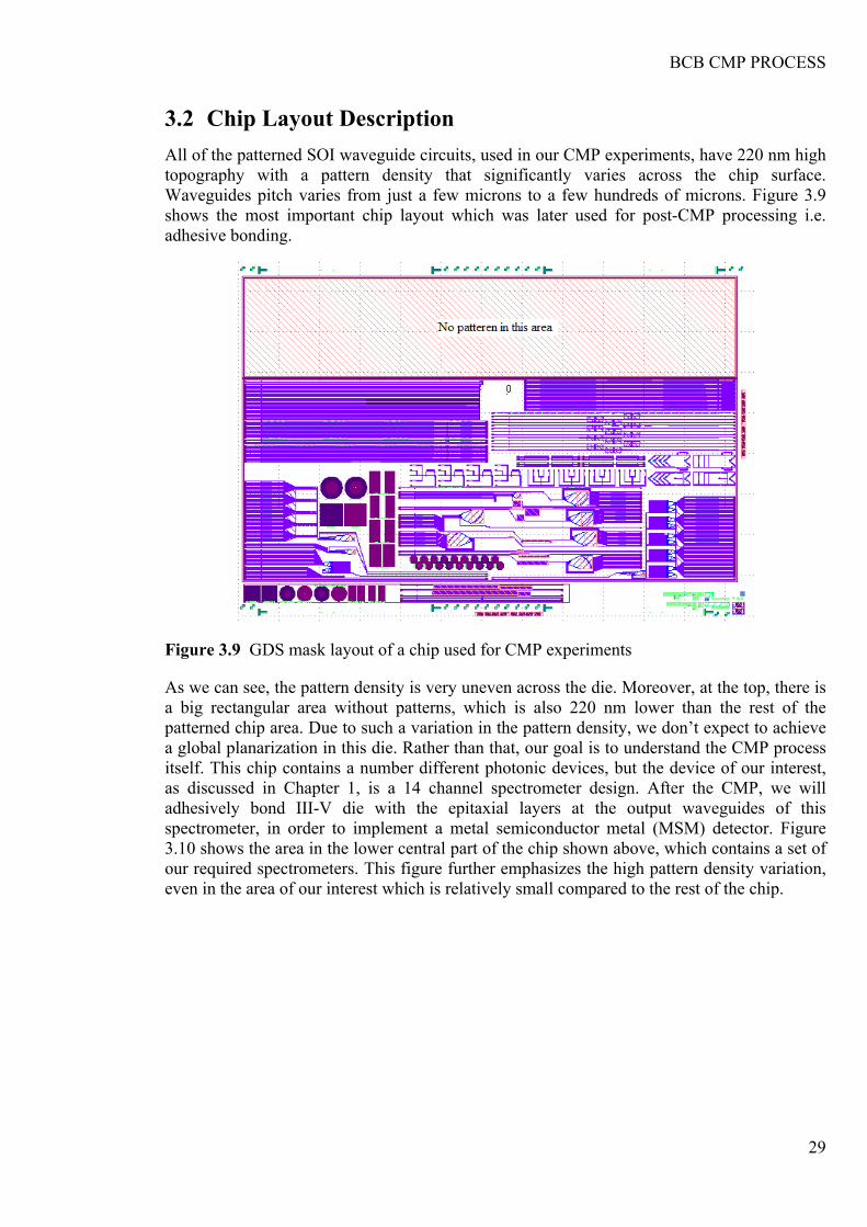
3.2 Chip Layout Description All of the patterned SOI waveguide circuits, used in our CMP experiments, have 220 nm high topography with a pattern density that significantly varies across the chip surface. Waveguides pitch varies from just a few microns to a few hundreds of microns. Figure 3.9 shows the most important chip layout which was later used for post-CMP processing i.e. adhesive bonding.
Figure 3.9 GDS mask layout of a chip used for CMP experiments
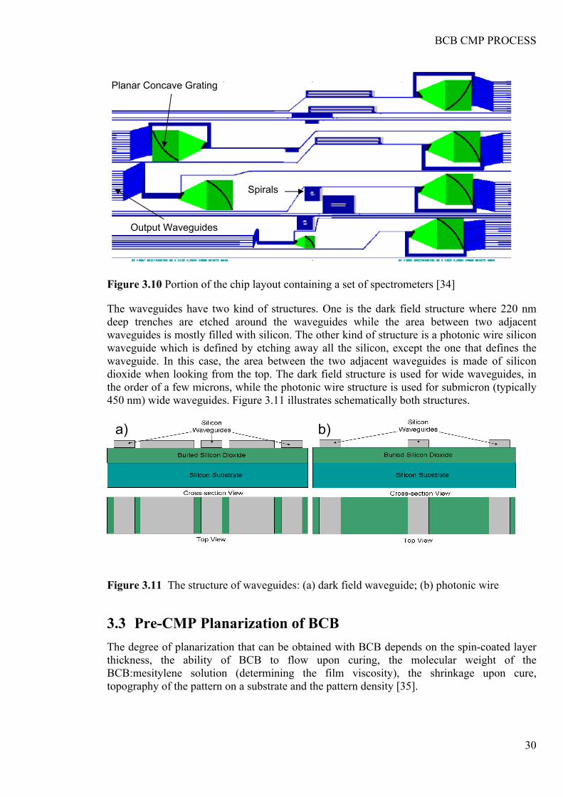
As we can see, the pattern density is very uneven across the die. Moreover, at the top, there is a big rectangular area without patterns, which is also 220 nm lower than the rest of the patterned chip area. Due to such a variation in the pattern density, we don’t expect to achieve a global planarization in this die. Rather than that, our goal is to understand the CMP process itself. This chip contains a number different photonic devices, but the device of our interest, as discussed in Chapter 1, is a 14 channel spectrometer design. After the CMP, we will adhesively bond III-V die with the epitaxial layers at the output waveguides of this spectrometer, in order to implement a metal semiconductor metal (MSM) detector. Figure 3.10 shows the area in the lower central part of the chip shown above, which contains a set of our required spectrometers. This figure further emphasizes the high pattern density variation, even in the area of our interest which is relatively small compared to the rest of the chip.
BCB CMP PROCESS
30
Figure 3.10 Portion of the chip layout containing a set of spectrometers [34]
The waveguides have two kind of structures. One is the dark field structure where 220 nm deep trenches are etched around the waveguides while the area between two adjacent waveguides is mostly filled with silicon. The other kind of structure is a photonic wire silicon waveguide which is defined by etching away all the silicon, except the one that defines the waveguide. In this case, the area between the two adjacent waveguides is made of silicon dioxide when looking from the top. The dark field structure is used for wide waveguides, in the order of a few microns, while the photonic wire structure is used for submicron (typically 450 nm) wide waveguides. Figure 3.11 illustrates schematically both structures.
Figure 3.11 The structure of waveguides: (a) dark field waveguide; (b) photonic wire
3.3 Pre-CMP Planarization of BCB The degree of planarization that can be obtained with BCB depends on the spin-coated layer thickness, the ability of BCB to flow upon curing, the molecular weight of the BCB:mesitylene solution (determining the film viscosity), the shrinkage upon cure, topography of the pattern on a substrate and the pattern density [35].
Planar Concave Grating
Spirals
Output Waveguides
a) b)
BCB CMP PROCESS
31
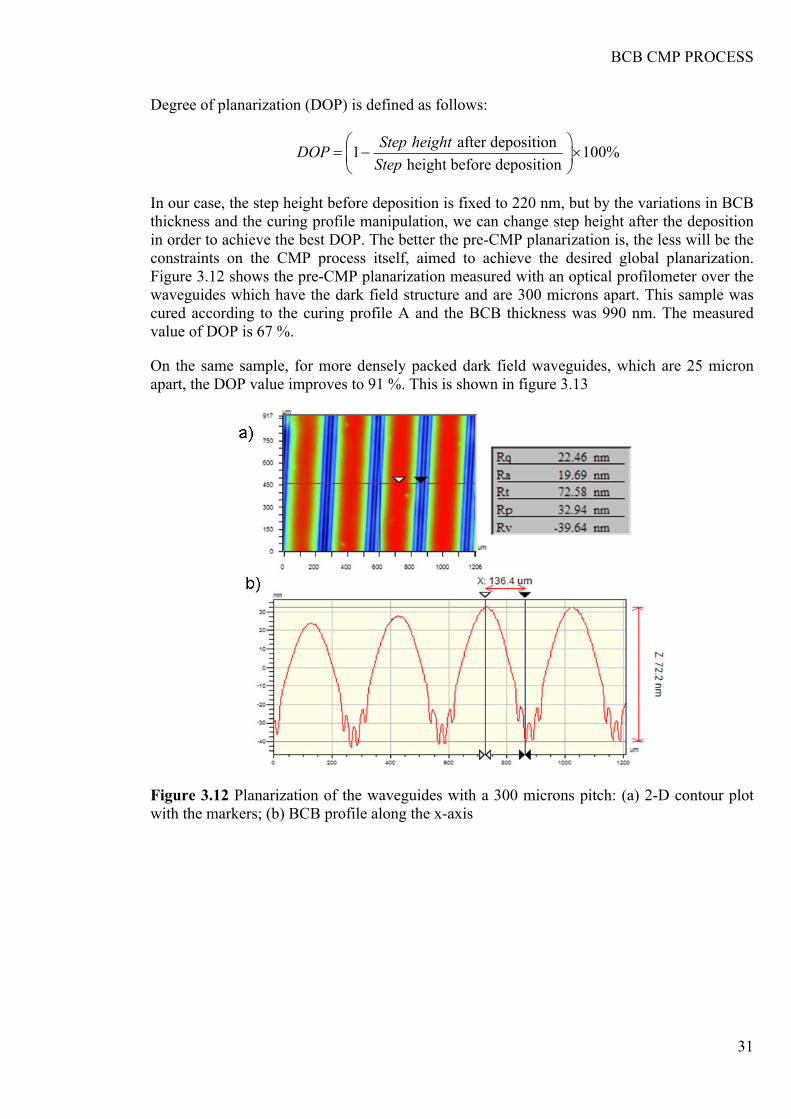
Degree of planarization (DOP) is defined as follows:
after deposition1 100% height before deposition
Step heightDOPStep
⎛ ⎞= − ×⎜ ⎟⎝ ⎠
In our case, the step height before deposition is fixed to 220 nm, but by the variations in BCB thickness and the curing profile manipulation, we can change step height after the deposition in order to achieve the best DOP. The better the pre-CMP planarization is, the less will be the constraints on the CMP process itself, aimed to achieve the desired global planarization. Figure 3.12 shows the pre-CMP planarization measured with an optical profilometer over the waveguides which have the dark field structure and are 300 microns apart. This sample was cured according to the curing profile A and the BCB thickness was 990 nm. The measured value of DOP is 67 %.
On the same sample, for more densely packed dark field waveguides, which are 25 micron apart, the DOP value improves to 91 %. This is shown in figure 3.13
Figure 3.12 Planarization of the waveguides with a 300 microns pitch: (a) 2-D contour plot with the markers; (b) BCB profile along the x-axis
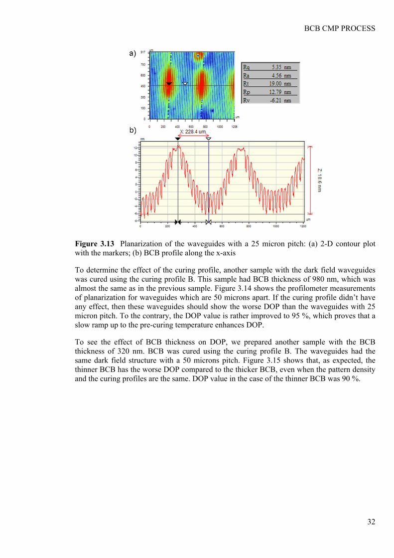
BCB CMP PROCESS
32
Figure 3.13 Planarization of the waveguides with a 25 micron pitch: (a) 2-D contour plot with the markers; (b) BCB profile along the x-axis
To determine the effect of the curing profile, another sample with the dark field waveguides was cured using the curing profile B. This sample had BCB thickness of 980 nm, which was almost the same as in the previous sample. Figure 3.14 shows the profilometer measurements of planarization for waveguides which are 50 microns apart. If the curing profile didn’t have any effect, then these waveguides should show the worse DOP than the waveguides with 25 micron pitch. To the contrary, the DOP value is rather improved to 95 %, which proves that a slow ramp up to the pre-curing temperature enhances DOP.
To see the effect of BCB thickness on DOP, we prepared another sample with the BCB thickness of 320 nm. BCB was cured using the curing profile B. The waveguides had the same dark field structure with a 50 microns pitch. Figure 3.15 shows that, as expected, the thinner BCB has the worse DOP compared to the thicker BCB, even when the pattern density and the curing profiles are the same. DOP value in the case of the thinner BCB was 90 %.
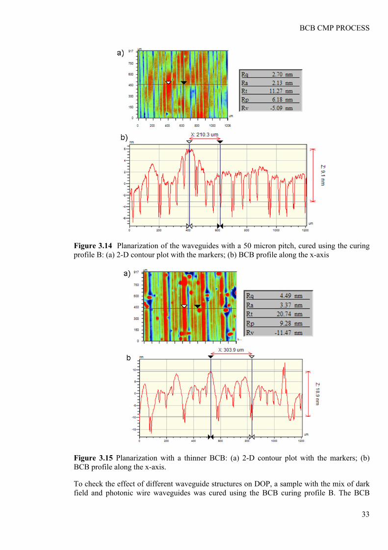
BCB CMP PROCESS
33
Figure 3.14 Planarization of the waveguides with a 50 micron pitch, cured using the curing profile B: (a) 2-D contour plot with the markers; (b) BCB profile along the x-axis
Figure 3.15 Planarization with a thinner BCB: (a) 2-D contour plot with the markers; (b) BCB profile along the x-axis.
To check the effect of different waveguide structures on DOP, a sample with the mix of dark field and photonic wire waveguides was cured using the BCB curing profile B. The BCB
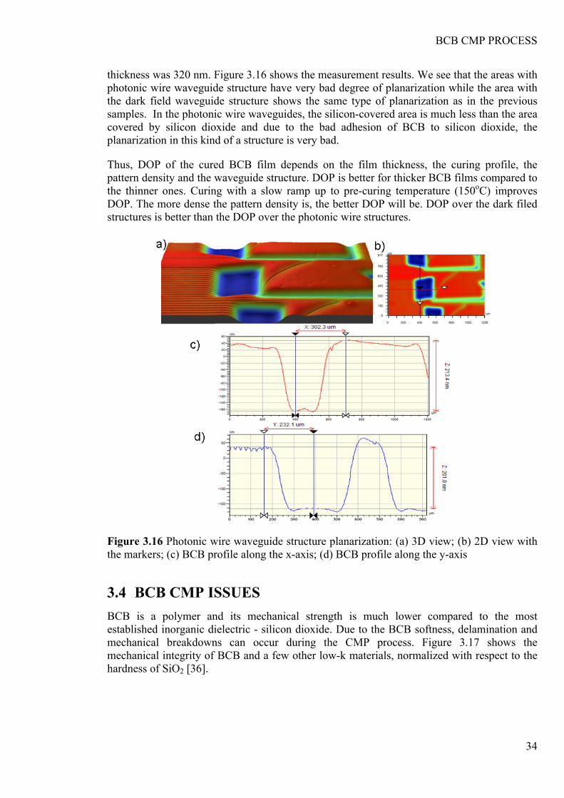
BCB CMP PROCESS
34
thickness was 320 nm. Figure 3.16 shows the measurement results. We see that the areas with photonic wire waveguide structure have very bad degree of planarization while the area with the dark field waveguide structure shows the same type of planarization as in the previous samples. In the photonic wire waveguides, the silicon-covered area is much less than the area covered by silicon dioxide and due to the bad adhesion of BCB to silicon dioxide, the planarization in this kind of a structure is very bad.
Thus, DOP of the cured BCB film depends on the film thickness, the curing profile, the pattern density and the waveguide structure. DOP is better for thicker BCB films compared to the thinner ones. Curing with a slow ramp up to pre-curing temperature (150oC) improves DOP. The more dense the pattern density is, the better DOP will be. DOP over the dark filed structures is better than the DOP over the photonic wire structures.
Figure 3.16 Photonic wire waveguide structure planarization: (a) 3D view; (b) 2D view with the markers; (c) BCB profile along the x-axis; (d) BCB profile along the y-axis
3.4 BCB CMP ISSUES BCB is a polymer and its mechanical strength is much lower compared to the most established inorganic dielectric - silicon dioxide. Due to the BCB softness, delamination and mechanical breakdowns can occur during the CMP process. Figure 3.17 shows the mechanical integrity of BCB and a few other low-k materials, normalized with respect to the hardness of SiO2 [36].
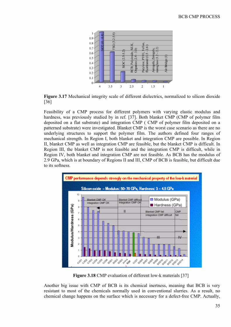
BCB CMP PROCESS
35
Figure 3.17 Mechanical integrity scale of different dielectrics, normalized to silicon dioxide [36]
Feasibility of a CMP process for different polymers with varying elastic modulus and hardness, was previously studied by in ref. [37]. Both blanket CMP (CMP of polymer film deposited on a flat substrate) and integration CMP ( CMP of polymer film deposited on a patterned substrate) were investigated. Blanket CMP is the worst case scenario as there are no underlying structures to support the polymer film. The authors defined four ranges of mechanical strength. In Region I, both blanket and integration CMP are possible. In Region II, blanket CMP as well as integration CMP are feasible, but the blanket CMP is difficult. In Region III, the blanket CMP is not feasible and the integration CMP is difficult, while in Region IV, both blanket and integration CMP are not feasible. As BCB has the modulus of 2.9 GPa, which is at boundary of Regions II and III, CMP of BCB is feasible, but difficult due to its softness.
Figure 3.18 CMP evaluation of different low-k materials [37]
Another big issue with CMP of BCB is its chemical inertness, meaning that BCB is very resistant to most of the chemicals normally used in conventional slurries. As a result, no chemical change happens on the surface which is necessary for a defect-free CMP. Actually,
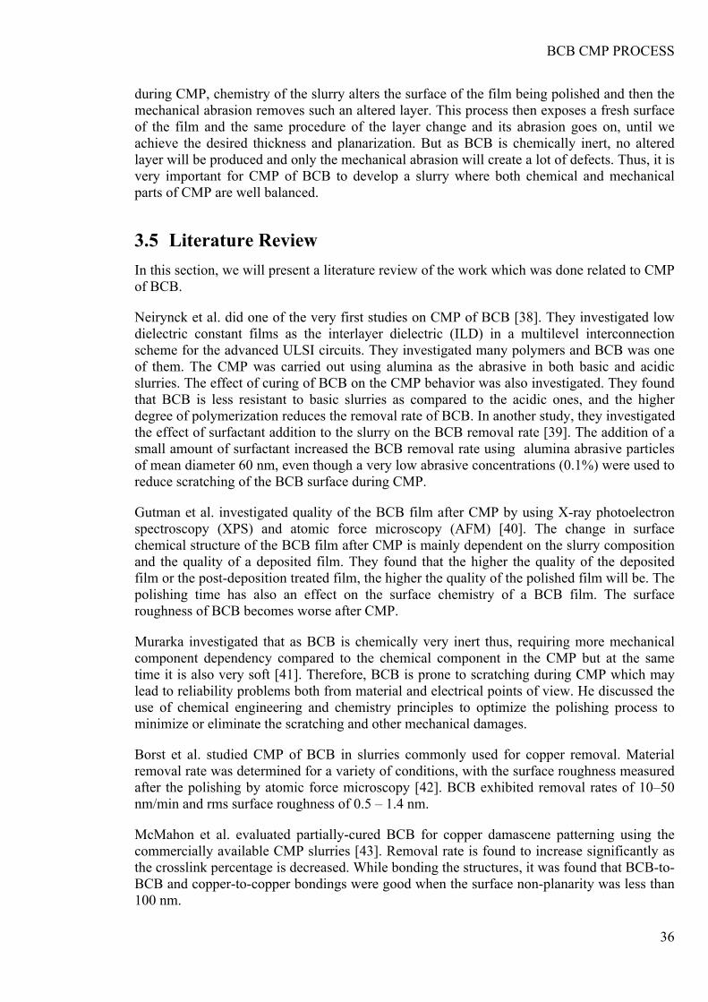
BCB CMP PROCESS
36
during CMP, chemistry of the slurry alters the surface of the film being polished and then the mechanical abrasion removes such an altered layer. This process then exposes a fresh surface of the film and the same procedure of the layer change and its abrasion goes on, until we achieve the desired thickness and planarization. But as BCB is chemically inert, no altered layer will be produced and only the mechanical abrasion will create a lot of defects. Thus, it is very important for CMP of BCB to develop a slurry where both chemical and mechanical parts of CMP are well balanced.
3.5 Literature Review In this section, we will present a literature review of the work which was done related to CMP of BCB.
Neirynck et al. did one of the very first studies on CMP of BCB [38]. They investigated low dielectric constant films as the interlayer dielectric (ILD) in a multilevel interconnection scheme for the advanced ULSI circuits. They investigated many polymers and BCB was one of them. The CMP was carried out using alumina as the abrasive in both basic and acidic slurries. The effect of curing of BCB on the CMP behavior was also investigated. They found that BCB is less resistant to basic slurries as compared to the acidic ones, and the higher degree of polymerization reduces the removal rate of BCB. In another study, they investigated the effect of surfactant addition to the slurry on the BCB removal rate [39]. The addition of a small amount of surfactant increased the BCB removal rate using alumina abrasive particles of mean diameter 60 nm, even though a very low abrasive concentrations (0.1%) were used to reduce scratching of the BCB surface during CMP.
Gutman et al. investigated quality of the BCB film after CMP by using X-ray photoelectron spectroscopy (XPS) and atomic force microscopy (AFM) [40]. The change in surface chemical structure of the BCB film after CMP is mainly dependent on the slurry composition and the quality of a deposited film. They found that the higher the quality of the deposited film or the post-deposition treated film, the higher the quality of the polished film will be. The polishing time has also an effect on the surface chemistry of a BCB film. The surface roughness of BCB becomes worse after CMP.
Murarka investigated that as BCB is chemically very inert thus, requiring more mechanical component dependency compared to the chemical component in the CMP but at the same time it is also very soft [41]. Therefore, BCB is prone to scratching during CMP which may lead to reliability problems both from material and electrical points of view. He discussed the use of chemical engineering and chemistry principles to optimize the polishing process to minimize or eliminate the scratching and other mechanical damages.
Borst et al. studied CMP of BCB in slurries commonly used for copper removal. Material removal rate was determined for a variety of conditions, with the surface roughness measured after the polishing by atomic force microscopy [42]. BCB exhibited removal rates of 10–50 nm/min and rms surface roughness of 0.5 – 1.4 nm.
McMahon et al. evaluated partially-cured BCB for copper damascene patterning using the commercially available CMP slurries [43]. Removal rate is found to increase significantly as the crosslink percentage is decreased. While bonding the structures, it was found that BCB-to-BCB and copper-to-copper bondings were good when the surface non-planarity was less than 100 nm.
BCB CMP PROCESS
37
Alireza et al. reported a novel fabrication process to develop planarized, isolated islands of BCB embedded in a silicon substrate (EBiS) [44]. They characterized CMP of BCB in detail since CMP is the key step in EBiS process. Atomic force microscopy (AFM) and elipsometry of the blanket BCB films before and after CMP, showed that the higher polishing downforce pressure and the higher speed lead to the higher removal rate at the expense of the higher surface roughness, non-uniformity, and scratch density. This was expected, since BCB is softer material compared to inorganic films such as silicon dioxide. They observed that as the cure temperature of BCB increases beyond 200oC, the CMP removal rate decreases drastically. The results obtained from optical microscopy, scanning electron microscopy, and optical profilometry showed excellent planarized surfaces on the EBiS islands.
Fei Geng et al. reported a wafer-level packaging structure with chips and passive components embedded in a silicon substrate for multichip modules (MCM) for radio frequency (RF) applications [45]. The BCB film was used as ILD. CMP was used to uncover the gold bumps in a fabrication process and the BCB curing profile was optimized to obtain the appropriate BCB film for a CMP process. In another study, the same authors used two layers of BCB films and three layers of metalized films, in which the monolithic microwave IC (MMIC), thin film resistors, strip-lines and micro-strip lines were integrated [46]. Here, they again used CMP to planarize the BCB films
We can conclude that most of the studies are either focused on studying the chemical effects of slurry using the blanket BCB films or CMP process is being used to implement some device structures. However, to our best knowledge, no study was related to the development of a CMP process to achieve ultra-thin and planarized BCB films on a patterned substrate which is the subject of this thesis.
CMP of BCB: Our Approach
38
4 CMP of BCB: Our Approach
In the previous chapter, we saw that most of the studies are either focused on studying the chemical effects of slurry using the blanket (BCB spin-coated and cured on an unpatterned Si substrate) BCB films or CMP process is being used to implement some device structures. However, to our best knowledge, no study was related to development of a complete CMP process (slurry, pad, process parameters) to achieve ultra-thin and planarized BCB films on patterned substrates, which is the subject of this thesis.
4.1 Our Approach CMP is a very complex process that involves a lot of output and input variables. Output variables include material removal rate, surface roughness, non-uniformity and step height ratio.
Material removal rate (MRR) is an average change in thickness of the film being polished per unit time. It is normally measured in nanometers per minute (nm/min).
Surface roughness is a measure of surface quality. It is actually high spatial frequency variations of film thickness. Both average values and rms values are used and measured in nanometers.
Non-uniformity (NU) is a measure of variation in MRR across the whole surface being polished. Mathematically, it is defined as:
max min 100%2 avg
MRR MRRNUMRR−
= ××
Step height ratio (SHR) is a measure of planarization of the wafer topography after CMP. It is defined as:
after CMP1 100% height before CMP
Step heightSHRStep
= − ×
Input variables are grouped as pad, slurry and the process parameters. The level of complexity increases because most of these variables are not independent, but rather related to each other. Figure 4.1 shows a complete set of input variables where the variables in bold are the ones which we considered for our CMP process development.
For development of BCB CMP process we used design of experiment (DoE) approach. We designed experiments to select suitable slurry, pad and the process parameters to achieve output variables values given in Table 4.1. These values were defined keeping in mind the requirements of our target application (adhesively bonding a III-V membrane on planarized SOI waveguide circuits to implement MSM photo-detectors).
Experiments were designed in three sets. The first set of experiments would focus on the choice of an optimum slurry, where we would try to achieve the target values for MRR and surface roughness, as these are the two output variables which are most influenced by the

CMP of BCB: Our Approach
39
slurry. After finding the right slurry, the next set of experiments would focus on finding the right pad to achieve the best planarization. The last set of experiments would focus on the process parameters to fine tune the whole CMP process.
Figure 4.1 A complete set of CMP variables
Output Variable
Target value
MRR > 40 nm/ min
Surface roughness < 25 nm
NU < 10 %
SHR > 50 %
Table 4.1 CMP output variables target values
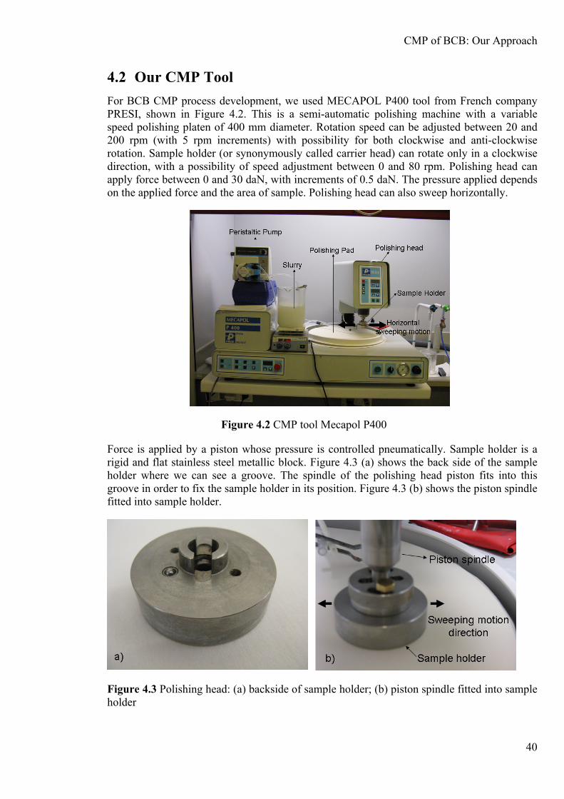
CMP of BCB: Our Approach
40
4.2 Our CMP Tool For BCB CMP process development, we used MECAPOL P400 tool from French company PRESI, shown in Figure 4.2. This is a semi-automatic polishing machine with a variable speed polishing platen of 400 mm diameter. Rotation speed can be adjusted between 20 and 200 rpm (with 5 rpm increments) with possibility for both clockwise and anti-clockwise rotation. Sample holder (or synonymously called carrier head) can rotate only in a clockwise direction, with a possibility of speed adjustment between 0 and 80 rpm. Polishing head can apply force between 0 and 30 daN, with increments of 0.5 daN. The pressure applied depends on the applied force and the area of sample. Polishing head can also sweep horizontally.
Figure 4.2 CMP tool Mecapol P400
Force is applied by a piston whose pressure is controlled pneumatically. Sample holder is a rigid and flat stainless steel metallic block. Figure 4.3 (a) shows the back side of the sample holder where we can see a groove. The spindle of the polishing head piston fits into this groove in order to fix the sample holder in its position. Figure 4.3 (b) shows the piston spindle fitted into sample holder.
Figure 4.3 Polishing head: (a) backside of sample holder; (b) piston spindle fitted into sample holder
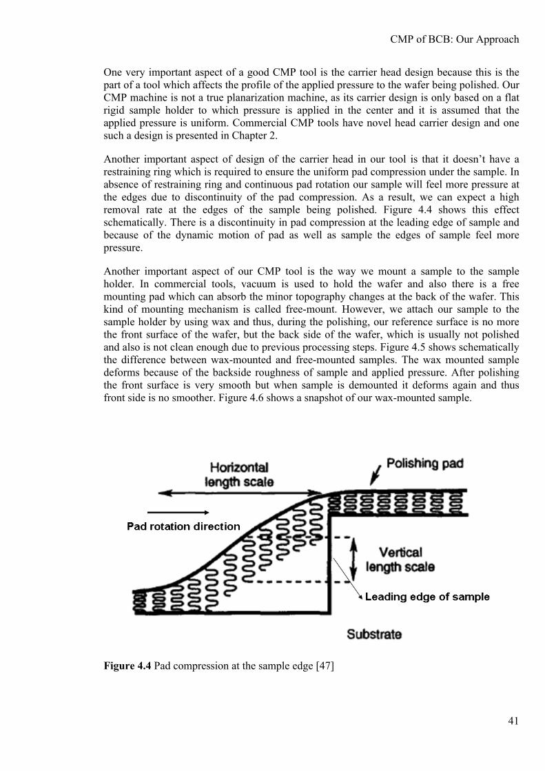
CMP of BCB: Our Approach
41
One very important aspect of a good CMP tool is the carrier head design because this is the part of a tool which affects the profile of the applied pressure to the wafer being polished. Our CMP machine is not a true planarization machine, as its carrier design is only based on a flat rigid sample holder to which pressure is applied in the center and it is assumed that the applied pressure is uniform. Commercial CMP tools have novel head carrier design and one such a design is presented in Chapter 2.
Another important aspect of design of the carrier head in our tool is that it doesn’t have a restraining ring which is required to ensure the uniform pad compression under the sample. In absence of restraining ring and continuous pad rotation our sample will feel more pressure at the edges due to discontinuity of the pad compression. As a result, we can expect a high removal rate at the edges of the sample being polished. Figure 4.4 shows this effect schematically. There is a discontinuity in pad compression at the leading edge of sample and because of the dynamic motion of pad as well as sample the edges of sample feel more pressure.
Another important aspect of our CMP tool is the way we mount a sample to the sample holder. In commercial tools, vacuum is used to hold the wafer and also there is a free mounting pad which can absorb the minor topography changes at the back of the wafer. This kind of mounting mechanism is called free-mount. However, we attach our sample to the sample holder by using wax and thus, during the polishing, our reference surface is no more the front surface of the wafer, but the back side of the wafer, which is usually not polished and also is not clean enough due to previous processing steps. Figure 4.5 shows schematically the difference between wax-mounted and free-mounted samples. The wax mounted sample deforms because of the backside roughness of sample and applied pressure. After polishing the front surface is very smooth but when sample is demounted it deforms again and thus front side is no smoother. Figure 4.6 shows a snapshot of our wax-mounted sample.
Figure 4.4 Pad compression at the sample edge [47]
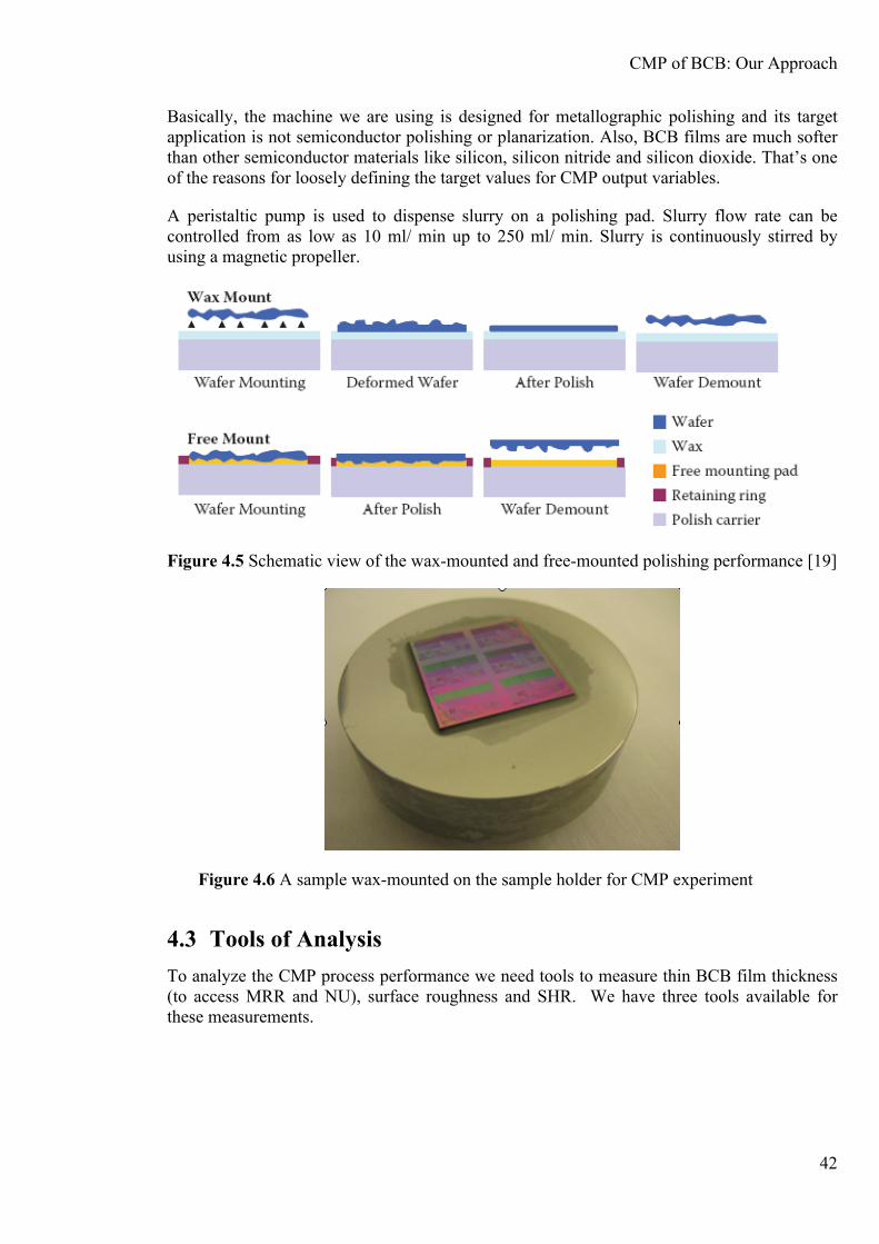
CMP of BCB: Our Approach
42
Basically, the machine we are using is designed for metallographic polishing and its target application is not semiconductor polishing or planarization. Also, BCB films are much softer than other semiconductor materials like silicon, silicon nitride and silicon dioxide. That’s one of the reasons for loosely defining the target values for CMP output variables.
A peristaltic pump is used to dispense slurry on a polishing pad. Slurry flow rate can be controlled from as low as 10 ml/ min up to 250 ml/ min. Slurry is continuously stirred by using a magnetic propeller.
Figure 4.5 Schematic view of the wax-mounted and free-mounted polishing performance [19]
Figure 4.6 A sample wax-mounted on the sample holder for CMP experiment
4.3 Tools of Analysis To analyze the CMP process performance we need tools to measure thin BCB film thickness (to access MRR and NU), surface roughness and SHR. We have three tools available for these measurements.
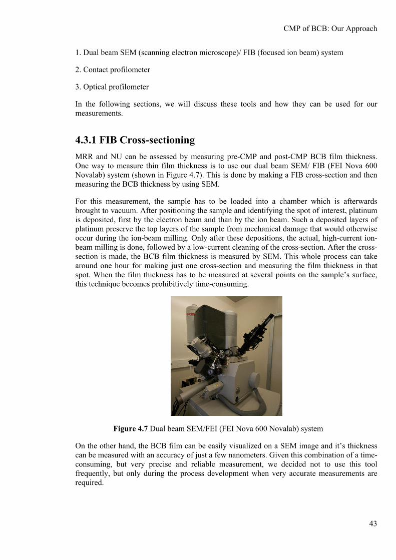
CMP of BCB: Our Approach
43
1. Dual beam SEM (scanning electron microscope)/ FIB (focused ion beam) system
2. Contact profilometer
3. Optical profilometer
In the following sections, we will discuss these tools and how they can be used for our measurements.
4.3.1 FIB Cross-sectioning MRR and NU can be assessed by measuring pre-CMP and post-CMP BCB film thickness. One way to measure thin film thickness is to use our dual beam SEM/ FIB (FEI Nova 600 Novalab) system (shown in Figure 4.7). This is done by making a FIB cross-section and then measuring the BCB thickness by using SEM.
For this measurement, the sample has to be loaded into a chamber which is afterwards brought to vacuum. After positioning the sample and identifying the spot of interest, platinum is deposited, first by the electron beam and than by the ion beam. Such a deposited layers of platinum preserve the top layers of the sample from mechanical damage that would otherwise occur during the ion-beam milling. Only after these depositions, the actual, high-current ion-beam milling is done, followed by a low-current cleaning of the cross-section. After the cross-section is made, the BCB film thickness is measured by SEM. This whole process can take around one hour for making just one cross-section and measuring the film thickness in that spot. When the film thickness has to be measured at several points on the sample’s surface, this technique becomes prohibitively time-consuming.
Figure 4.7 Dual beam SEM/FEI (FEI Nova 600 Novalab) system
On the other hand, the BCB film can be easily visualized on a SEM image and it’s thickness can be measured with an accuracy of just a few nanometers. Given this combination of a time-consuming, but very precise and reliable measurement, we decided not to use this tool frequently, but only during the process development when very accurate measurements are required.
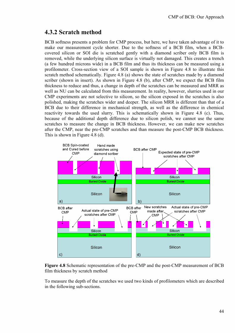
CMP of BCB: Our Approach
44
4.3.2 Scratch method BCB softness presents a problem for CMP process, but here, we have taken advantage of it to make our measurement cycle shorter. Due to the softness of a BCB film, when a BCB-covered silicon or SOI die is scratched gently with a diamond scriber only BCB film is removed, while the underlying silicon surface is virtually not damaged. This creates a trench (a few hundred microns wide) in a BCB film and thus its thickness can be measured using a profilometer. Cross-section view of a SOI sample is shown in Figure 4.8 to illustrate this scratch method schematically. Figure 4.8 (a) shows the state of scratches made by a diamond scriber (shown in insert). As shown in Figure 4.8 (b), after CMP, we expect the BCB film thickness to reduce and thus, a change in depth of the scratches can be measured and MRR as well as NU can be calculated from this measurement. In reality, however, slurries used in our CMP experiments are not selective to silicon, so the silicon exposed in the scratches is also polished, making the scratches wider and deeper. The silicon MRR is different than that of a BCB due to their difference in mechanical strength, as well as the difference in chemical reactivity towards the used slurry. This is schematically shown in Figure 4.8 (c). Thus, because of the additional depth difference due to silicon polish, we cannot use the same scratches to measure the change in BCB thickness. However, we can make new scratches after the CMP, near the pre-CMP scratches and than measure the post-CMP BCB thickness. This is shown in Figure 4.8 (d).
Figure 4.8 Schematic representation of the pre-CMP and the post-CMP measurement of BCB film thickness by scratch method
To measure the depth of the scratches we used two kinds of profilometers which are described in the following sub-sections.
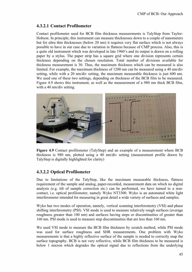
CMP of BCB: Our Approach
45
4.3.2.1 Contact Profilometer
Contact profilometer used for BCB film thickness measurements is TalyStep from Taylor-Hobson. In principle, this instrument can measure thicknesses down to a couple of nanometers but for ultra thin thicknesses (below 20 nm) it requires very flat surface which is not always possible to have in our case due to variation in flatness because of CMP process. Also, this is a quite old instrument which was developed in late 1960’s and its output is drawn on a rolling paper by a stylus. The paper strip has a square grid where one division represents certain thickness depending on the chosen resolution. Total number of divisions available for thickness measurement is 30. Thus, the maximum thickness which can be measured is also limited. For example, the maximum thickness of 1200 nm can be measured using a 40 nm/div setting, while with a 20 nm/div setting, the maximum measurable thickness is just 600 nm. We used one of these two settings, depending on thickness of the BCB film to be measured. Figure 4.9 shows this instrument, as well as the measurement of a 980 nm thick BCB film, with a 40 nm/div setting.
Figure 4.9 Contact profilometer (TalyStep) and an example of a measurement where BCB thickness is 980 nm, plotted using a 40 nm/div setting (measurement profile drawn by TalyStep is digitally highlighted for clarity)
4.3.2.2 Optical Profilometer
Due to limitations of the TalyStep, like the maximum measurable thickness, flatness requirement of the sample and analog, paper-recorded, measurement data on which no digital analysis (e.g. tilt of sample correction etc.) can be performed, we have turned to a non-contact, i.e. optical profilometer, namely Wyko NT3300. Wyko is an automated white light interferometer intended for measuring in great detail a wide variety of surfaces and samples.
Wyko has two modes of operation, namely, vertical scanning interferometry (VSI) and phase shifting interferometry (PSI). VSI mode is used to measure relatively rough surfaces (average roughness greater than 100 nm) and surfaces having steps or discontinuities of greater than 160 nm. PSI mode is used to measure step discontinuities that are less than 160 nm.
We used VSI mode to measure the BCB film thickness by scratch method, while PSI mode was used for surface roughness and SHR measurements. One problem with Wyko measurements is that a highly reflective surface of the sample is needed to correctly map the surface topography. BCB is not very reflective, while BCB film thickness to be measured is below 1 micron which degrades the optical signal due to reflections from the underlying
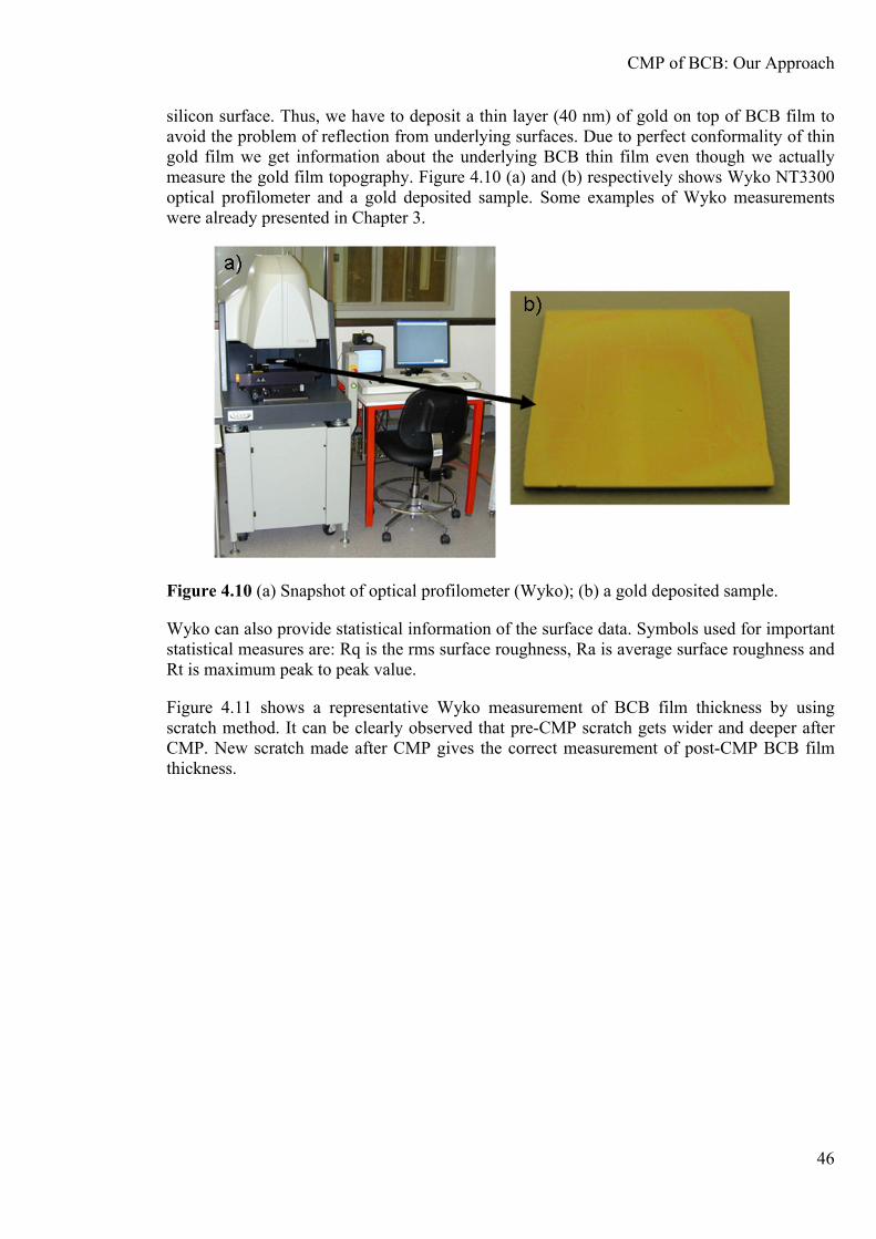
CMP of BCB: Our Approach
46
silicon surface. Thus, we have to deposit a thin layer (40 nm) of gold on top of BCB film to avoid the problem of reflection from underlying surfaces. Due to perfect conformality of thin gold film we get information about the underlying BCB thin film even though we actually measure the gold film topography. Figure 4.10 (a) and (b) respectively shows Wyko NT3300 optical profilometer and a gold deposited sample. Some examples of Wyko measurements were already presented in Chapter 3.
Figure 4.10 (a) Snapshot of optical profilometer (Wyko); (b) a gold deposited sample.
Wyko can also provide statistical information of the surface data. Symbols used for important statistical measures are: Rq is the rms surface roughness, Ra is average surface roughness and Rt is maximum peak to peak value.
Figure 4.11 shows a representative Wyko measurement of BCB film thickness by using scratch method. It can be clearly observed that pre-CMP scratch gets wider and deeper after CMP. New scratch made after CMP gives the correct measurement of post-CMP BCB film thickness.

CMP of BCB: Our Approach
47
Figure 4.11 Wyko measurement of BCB film thickness by using scratch method: (a) 3D view; (b) Horizontal Profile of BCB thickness.
To summarize, TalyStep measurements are used for quick feedback on the performance of CMP process development as no special treatment of the sample to be measured is needed. For more detailed and accurate measurements, Wyko is used after gold deposition on the sample surface. For very precise and highly reliable measurements, FIB cross-sections are made and imaged.
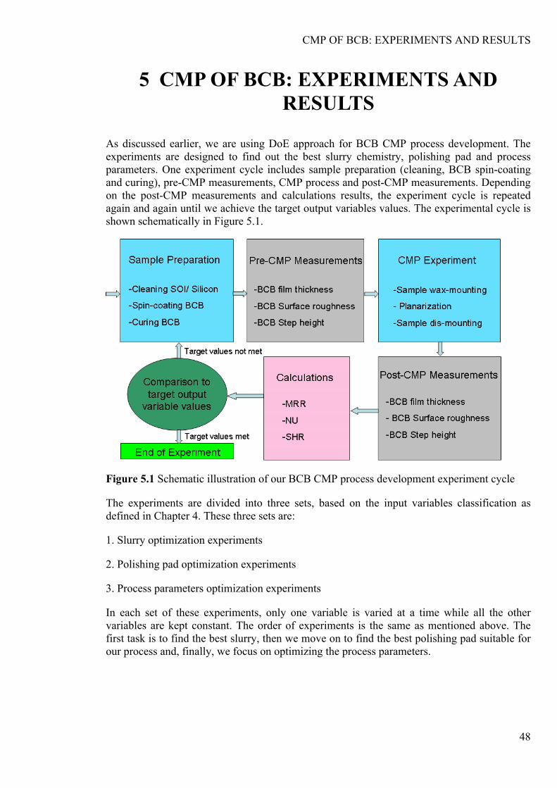
CMP OF BCB: EXPERIMENTS AND RESULTS
48
5 CMP OF BCB: EXPERIMENTS AND RESULTS
As discussed earlier, we are using DoE approach for BCB CMP process development. The experiments are designed to find out the best slurry chemistry, polishing pad and process parameters. One experiment cycle includes sample preparation (cleaning, BCB spin-coating and curing), pre-CMP measurements, CMP process and post-CMP measurements. Depending on the post-CMP measurements and calculations results, the experiment cycle is repeated again and again until we achieve the target output variables values. The experimental cycle is shown schematically in Figure 5.1.
Figure 5.1 Schematic illustration of our BCB CMP process development experiment cycle
The experiments are divided into three sets, based on the input variables classification as defined in Chapter 4. These three sets are:
1. Slurry optimization experiments
2. Polishing pad optimization experiments
3. Process parameters optimization experiments
In each set of these experiments, only one variable is varied at a time while all the other variables are kept constant. The order of experiments is the same as mentioned above. The first task is to find the best slurry, then we move on to find the best polishing pad suitable for our process and, finally, we focus on optimizing the process parameters.
CMP OF BCB: EXPERIMENTS AND RESULTS
49
5.1 Slurry Optimization: Experiments and Results For slurry optimization experiments, the output variables of interest are MRR and surface roughness. For the initial experiments, a 100 mm blank silicon wafer was cleaned using SC-1. After this, BCB was spin-coated and cured using BCB curing profile B discussed in Chapter 3. However, in the initial experiments, we didn’t use the adhesion promoter prior to BCB spin-coating. After curing, the wafer was cleaved into small sample dies of 20 mm x 20 mm. Pre-CMP thickness was measured using scratch method and TalyStep. This thickness was 960 ± 20 nm for different samples, depending on the part of wafer from which the sample was taken (spin-coating process produces a slightly thicker film at the edges of the wafer as compared to the center). After the thickness measurements, sample was wax-mounted to the sample holder.
Commercial slurry from PRESI was used in these experiments. The slurry designation is SPM and is based on colloidal silica abrasive particles with 30-40 nm mean diameter and concentration of 50 % by weight. This concentration is very high for our application, as BCB is very soft and such a high concentration of abrasive particles can produce scratches. Therefore, the original slurry was diluted to SPM: H2O (1:4). The pH value of this slurry was between 10 and 10.5. Polishing pad used was LDR1 from PRESI. This pad has relatively moderate shore A hardness value of 74 and small compressibility of 3.6 %. Shore hardness is a measure of the resistance of material to indentation by 3 spring-loaded indenter [48]. The initial experiments failed, since the BCB film peeled-off from the silicon substrate within the first minute of a CMP, Images of a few samples, after a couple of tens of seconds of CMP are shown in Figure 5.2. One possible reason for this delamination was thought to be a high mechanical part of a CMP process, due to pressure and velocity. Thus, we repeated the experiment with a lower force and velocity and Figures 5.2 (b) and (c) show the effect of the reduced mechanical part of a CMP, though BCB film had still delaminated. Subsequent experiments showed that this problem was related to a poor adhesion of BCB to the silicon wafer surface. A thin native oxide is present on a silicon wafer surface and as BCB adhesion to SiO2 is not good, the BCB film peels off during the CMP. This problem was solved by using the adhesion promoter before spin-coating of BCB on silicon wafer surface.
The following experiments, after applying the adhesion promoter AP3000, showed no delamination, but the MRR was very low. While using the pressure of 24.8 kPa and pad rotation velocity of 45 rpm, MRR remained within the range of 5 to 10 nm, for different samples. Figure 5.3 shows images of two samples after this CMP process. Sample shown in Figure 5.3 (a) has the BCB film removed on the edges. This problem we call the edge effect and it occurs due to pressure discontinuity at the sample edges. This effect depends also on the CMP process duration. The sample in Figure 5.3 (a) was polished for 5 minutes, while the sample in Figure 5.3 (b) was polished for 10 minutes. This problem was discussed in detail in Chapter 4. A small difference in MRR can be due to the variation of pressure as cleaved samples cannot have exactly the same area.
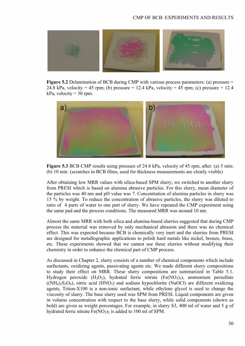
CMP OF BCB: EXPERIMENTS AND RESULTS
50
Figure 5.2 Delamination of BCB during CMP with various process parameters: (a) pressure = 24.8 kPa, velocity = 45 rpm; (b) pressure = 12.4 kPa, velocity = 45 rpm; (c) pressure = 12.4 kPa, velocity = 30 rpm.
Figure 5.3 BCB CMP results using pressure of 24.8 kPa, velocity of 45 rpm, after: (a) 5 min; (b) 10 min (scratches in BCB films, used for thickness measurements are clearly visible)
After obtaining low MRR values with silica-based SPM slurry, we switched to another slurry from PRESI which is based on alumina abrasive particles. For this slurry, mean diameter of the particles was 40 nm and pH value was 7. Concentration of alumina particles in slurry was 15 % by weight. To reduce the concentration of abrasive particles, the slurry was diluted to ratio of 4 parts of water to one part of slurry. We have repeated the CMP experiment using the same pad and the process conditions. The measured MRR was around 10 nm.
Almost the same MRR with both silica and alumina-based slurries suggested that during CMP process the material was removed by only mechanical abrasion and there was no chemical effect. This was expected because BCB is chemically very inert and the slurries from PRESI are designed for metallographic applications to polish hard metals like nickel, bronze, brass, etc. These experiments showed that we cannot use these slurries without modifying their chemistry in order to enhance the chemical part of CMP process.
As discussed in Chapter 2, slurry consists of a number of chemical components which include surfactants, oxidizing agents, passivating agents etc. We made different slurry compositions to study their effect on MRR. These slurry compositions are summarized in Table 5.1. Hydrogen peroxide (H2O2), hydrated ferric nitrate (Fe(NO3)3), ammonium persulfate ((NH4)2S2O8), nitric acid (HNO3) and sodium hypochlorite (NaOCl) are different oxidizing agents, Triton-X100 is a non-ionic surfactant, while ethylene glycol is used to change the viscosity of slurry. The base slurry used was SPM from PRESI. Liquid components are given in volume concentration with respect to the base slurry, while solid components (shown as bold) are given as weight percentages. For example, in slurry S3, 400 ml of water and 5 g of hydrated ferric nitrate Fe(NO3)3 is added to 100 ml of SPM.
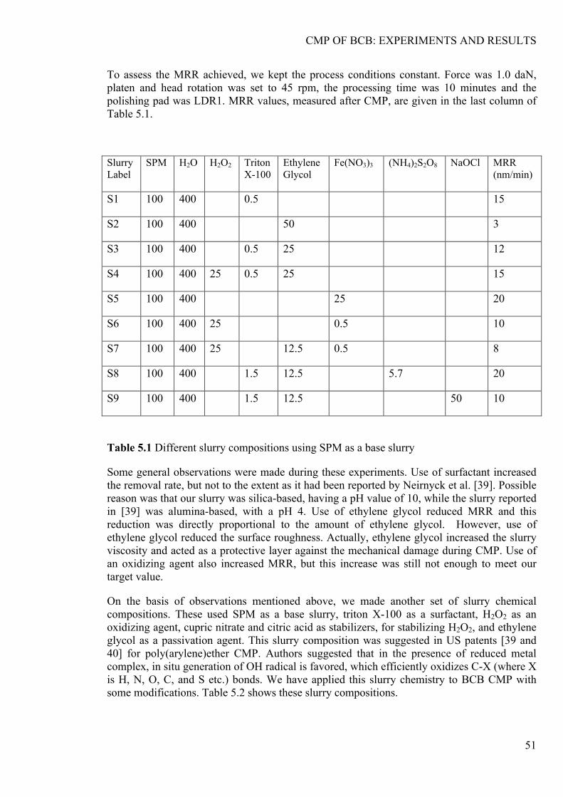
CMP OF BCB: EXPERIMENTS AND RESULTS
51
To assess the MRR achieved, we kept the process conditions constant. Force was 1.0 daN, platen and head rotation was set to 45 rpm, the processing time was 10 minutes and the polishing pad was LDR1. MRR values, measured after CMP, are given in the last column of Table 5.1.
Slurry Label
SPM H2O H2O2 Triton X-100
Ethylene Glycol
Fe(NO3)3 (NH4)2S2O8 NaOCl MRR (nm/min)
S1 100 400 0.5 15
S2 100 400 50 3
S3 100 400 0.5 25 12
S4 100 400 25 0.5 25 15
S5 100 400 25 20
S6 100 400 25 0.5 10
S7 100 400 25 12.5 0.5 8
S8 100 400 1.5 12.5 5.7 20
S9 100 400 1.5 12.5 50 10
Table 5.1 Different slurry compositions using SPM as a base slurry
Some general observations were made during these experiments. Use of surfactant increased the removal rate, but not to the extent as it had been reported by Neirnyck et al. [39]. Possible reason was that our slurry was silica-based, having a pH value of 10, while the slurry reported in [39] was alumina-based, with a pH 4. Use of ethylene glycol reduced MRR and this reduction was directly proportional to the amount of ethylene glycol. However, use of ethylene glycol reduced the surface roughness. Actually, ethylene glycol increased the slurry viscosity and acted as a protective layer against the mechanical damage during CMP. Use of an oxidizing agent also increased MRR, but this increase was still not enough to meet our target value.
On the basis of observations mentioned above, we made another set of slurry chemical compositions. These used SPM as a base slurry, triton X-100 as a surfactant, H2O2 as an oxidizing agent, cupric nitrate and citric acid as stabilizers, for stabilizing H2O2, and ethylene glycol as a passivation agent. This slurry composition was suggested in US patents [39 and 40] for poly(arylene)ether CMP. Authors suggested that in the presence of reduced metal complex, in situ generation of OH radical is favored, which efficiently oxidizes C-X (where X is H, N, O, C, and S etc.) bonds. We have applied this slurry chemistry to BCB CMP with some modifications. Table 5.2 shows these slurry compositions.
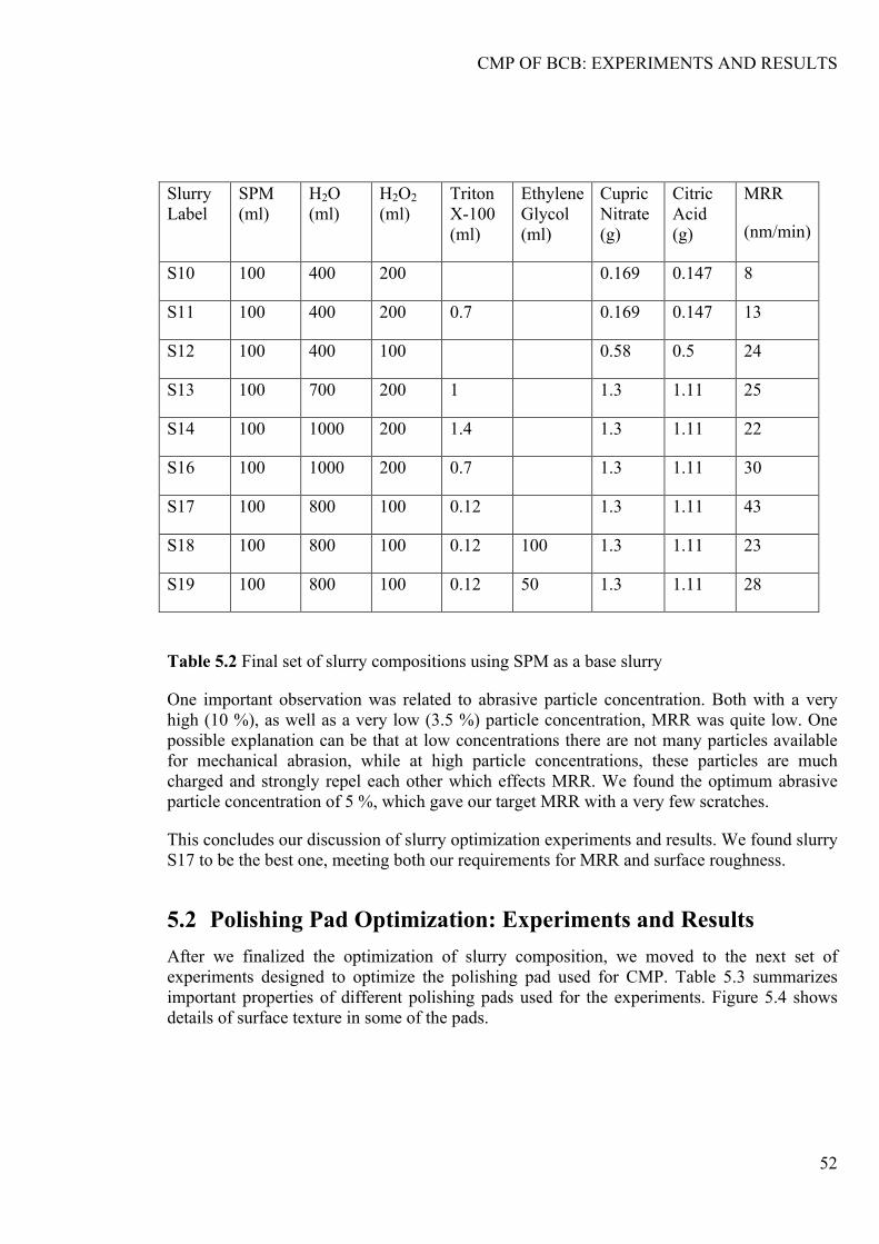
CMP OF BCB: EXPERIMENTS AND RESULTS
52
Slurry Label
SPM (ml)
H2O (ml)
H2O2 (ml)
Triton X-100 (ml)
Ethylene Glycol (ml)
Cupric Nitrate (g)
Citric Acid (g)
MRR
(nm/min)
S10 100 400 200 0.169 0.147 8
S11 100 400 200 0.7 0.169 0.147 13
S12 100 400 100 0.58 0.5 24
S13 100 700 200 1 1.3 1.11 25
S14 100 1000 200 1.4 1.3 1.11 22
S16 100 1000 200 0.7 1.3 1.11 30
S17 100 800 100 0.12 1.3 1.11 43
S18 100 800 100 0.12 100 1.3 1.11 23
S19 100 800 100 0.12 50 1.3 1.11 28
Table 5.2 Final set of slurry compositions using SPM as a base slurry
One important observation was related to abrasive particle concentration. Both with a very high (10 %), as well as a very low (3.5 %) particle concentration, MRR was quite low. One possible explanation can be that at low concentrations there are not many particles available for mechanical abrasion, while at high particle concentrations, these particles are much charged and strongly repel each other which effects MRR. We found the optimum abrasive particle concentration of 5 %, which gave our target MRR with a very few scratches.
This concludes our discussion of slurry optimization experiments and results. We found slurry S17 to be the best one, meeting both our requirements for MRR and surface roughness.
5.2 Polishing Pad Optimization: Experiments and Results After we finalized the optimization of slurry composition, we moved to the next set of experiments designed to optimize the polishing pad used for CMP. Table 5.3 summarizes important properties of different polishing pads used for the experiments. Figure 5.4 shows details of surface texture in some of the pads.
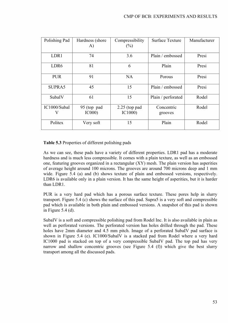
CMP OF BCB: EXPERIMENTS AND RESULTS
53
Polishing Pad Hardness (shore A)
Compressibility (%)
Surface Texture Manufacturer
LDR1 74 3.6 Plain / embossed Presi
LDR6 81 6 Plain Presi
PUR 91 NA Porous Presi
SUPRA5 45 15 Plain / embossed Presi
SubaIV 61 15 Plain / perforated Rodel
IC1000/SubaIV
95 (top pad IC000)
2.25 (top pad IC1000)
Concentric grooves
Rodel
Politex Very soft 15 Plain Rodel
Table 5.3 Properties of different polishing pads
As we can see, these pads have a variety of different properties. LDR1 pad has a moderate hardness and is much less compressible. It comes with a plain texture, as well as an embossed one, featuring grooves organized in a rectangular (XY) mesh. The plain version has asperities of average height around 100 microns. The grooves are around 700 microns deep and 1 mm wide. Figure 5.4 (a) and (b) shows texture of plain and embossed versions, respectively. LDR6 is available only in a plain version. It has the same height of asperities, but it is harder than LDR1.
PUR is a very hard pad which has a porous surface texture. These pores help in slurry transport. Figure 5.4 (c) shows the surface of this pad. Supra5 is a very soft and compressible pad which is available in both plain and embossed versions. A snapshot of this pad is shown in Figure 5.4 (d).
SubaIV is a soft and compressible polishing pad from Rodel Inc. It is also available in plain as well as perforated versions. The perforated version has holes drilled through the pad. These holes have 2mm diameter and 4.5 mm pitch. Image of a perforated SubaIV pad surface is shown in Figure 5.4 (e). IC1000/SubaIV is a stacked pad from Rodel where a very hard IC1000 pad is stacked on top of a very compressible SubaIV pad. The top pad has very narrow and shallow concentric grooves (see Figure 5.4 (f)) which give the best slurry transport among all the discussed pads.

CMP OF BCB: EXPERIMENTS AND RESULTS
54
Figure 5.4 Polishing pads surface texture: (a) LDR1 plain; (b) LDR1 embossed; (c) SubaIV perforated; (d) Supra5 embossed; (e) PUR; (f) Stacked IC1000/SubaIV
During the study of slurry chemistry, we ignored non-uniformity of the removal rate. Figure 5.5 shows the non-uniformity of removal rate for samples polished using LDR1 pad and different slurry chemistries. These samples were polished using the same pad (LDR1), the same pressure (24.8 kPa), the same velocity (45 rpm) and the same processing time (10 min).
Figure 5.5 Samples polished on LDR1 polishing pad using different slurries: (a) slurry S7, MRR = 8 nm/min; (b) slurry S3, MRR = 12 nm/min; (c) slurry S8, MRR = 20 nm/min.
We can clearly see the number of fringes increasing as the MRR increases. We believe that this is caused by a poor slurry transport ability of the pad. Slurry is not able to reach the center of the sample and that’s why much less material is removed at the center as compared to the edges. At the start of experiment, slurry removes material at the edges and, as polishing continues, this thinner BCB film at the edges allows slurry to penetrate a bit further towards the center. This cycle goes on to produce more and more fringes. The number of fringes is low for the samples with a low MRR because not enough material is being removed at the edges to allow slurry penetration towards the center.
To check our hypothesis that the appearance of these fringes is caused by poor slurry transport, we used an embossed LDR1 pad. However, samples were very badly damaged when we performed a CMP with this pad. The damage occurred mainly because the grooves between the embossed islands were very deep (around 700 microns) and wide (around 1 mm). Although the slurry transport should have been, in principal, better with these grooves, in reality, due to a limited flow rate, the slurry mostly stayed in the grooves and the surface of
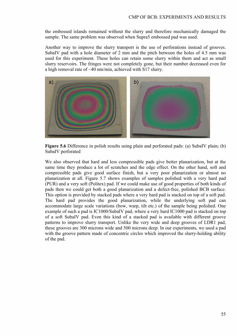
CMP OF BCB: EXPERIMENTS AND RESULTS
55
the embossed islands remained without the slurry and therefore mechanically damaged the sample. The same problem was observed when Supra5 embossed pad was used.
Another way to improve the slurry transport is the use of perforations instead of grooves. SubaIV pad with a hole diameter of 2 mm and the pitch between the holes of 4.5 mm was used for this experiment. These holes can retain some slurry within them and act as small slurry reservoirs. The fringes were not completely gone, but their number decreased even for a high removal rate of ~40 nm/min, achieved with S17 slurry.
Figure 5.6 Difference in polish results using plain and perforated pads: (a) SubaIV plain; (b) SubaIV perforated
We also observed that hard and less compressible pads give better planarization, but at the same time they produce a lot of scratches and the edge effect. On the other hand, soft and compressible pads give good surface finish, but a very poor planarization or almost no planarization at all. Figure 5.7 shows examples of samples polished with a very hard pad (PUR) and a very soft (Politex) pad. If we could make use of good properties of both kinds of pads then we could get both a good planarization and a defect-free, polished BCB surface. This option is provided by stacked pads where a very hard pad is stacked on top of a soft pad. The hard pad provides the good planarization, while the underlying soft pad can accommodate large scale variations (bow, warp, tilt etc.) of the sample being polished. One example of such a pad is IC1000/SubaIV pad, where a very hard IC1000 pad is stacked on top of a soft SubaIV pad. Even this kind of a stacked pad is available with different groove patterns to improve slurry transport. Unlike the very wide and deep grooves of LDR1 pad, these grooves are 300 microns wide and 500 microns deep. In our experiments, we used a pad with the groove pattern made of concentric circles which improved the slurry-holding ability of the pad.
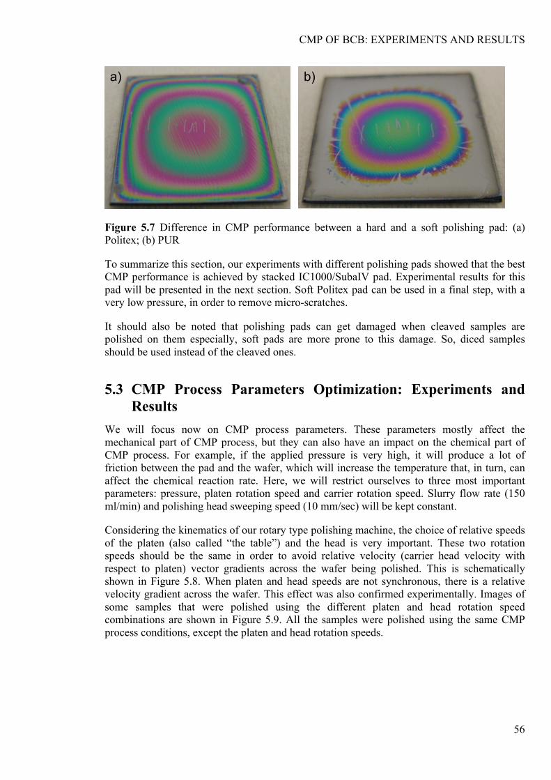
CMP OF BCB: EXPERIMENTS AND RESULTS
56
Figure 5.7 Difference in CMP performance between a hard and a soft polishing pad: (a) Politex; (b) PUR
To summarize this section, our experiments with different polishing pads showed that the best CMP performance is achieved by stacked IC1000/SubaIV pad. Experimental results for this pad will be presented in the next section. Soft Politex pad can be used in a final step, with a very low pressure, in order to remove micro-scratches.
It should also be noted that polishing pads can get damaged when cleaved samples are polished on them especially, soft pads are more prone to this damage. So, diced samples should be used instead of the cleaved ones.
5.3 CMP Process Parameters Optimization: Experiments and Results
We will focus now on CMP process parameters. These parameters mostly affect the mechanical part of CMP process, but they can also have an impact on the chemical part of CMP process. For example, if the applied pressure is very high, it will produce a lot of friction between the pad and the wafer, which will increase the temperature that, in turn, can affect the chemical reaction rate. Here, we will restrict ourselves to three most important parameters: pressure, platen rotation speed and carrier rotation speed. Slurry flow rate (150 ml/min) and polishing head sweeping speed (10 mm/sec) will be kept constant.
Considering the kinematics of our rotary type polishing machine, the choice of relative speeds of the platen (also called “the table”) and the head is very important. These two rotation speeds should be the same in order to avoid relative velocity (carrier head velocity with respect to platen) vector gradients across the wafer being polished. This is schematically shown in Figure 5.8. When platen and head speeds are not synchronous, there is a relative velocity gradient across the wafer. This effect was also confirmed experimentally. Images of some samples that were polished using the different platen and head rotation speed combinations are shown in Figure 5.9. All the samples were polished using the same CMP process conditions, except the platen and head rotation speeds.
a) b)

CMP OF BCB: EXPERIMENTS AND RESULTS
57
Figure 5.8 Schematic illustration of the relative velocity vectors for different combinations of carrier head and platen rotation speeds [51]
Figure 5.9 Effect of the difference in platen and head rotation speeds: (a) platen speed of 45 rpm and head speed of 30 rpm; (b) platen speed of 45 rpm and head speed of 20 rpm; (c) both platen and head speeds were 45 rpm, but the sample was mounted off-centered
All of the samples shown above exhibit the non-uniformity in form of the fringes (which is basically due to the poor slurry transport), but we can clearly observe that these fringes are off-centered when the table and head speeds are different, as shown in Figure 5.9 (a) and Figure 5.9 (b). However, when both platen and head speeds are the same, fringes are concentrically positioned around the center of the sample, as shown in Figure 5.9 (d). Figure 5.9 (c) shows a sample for which off-centered fringes appeared even though the sample was polished using the same platen and head speeds. However, this sample was mounted off-centered on the sample holder which might have changed the pressure profile across the sample. We can conclude that the sample should be mounted at the center of the sample holder, while platen and head speeds as well as their direction of rotation should be the same in order to avoid the non-uniformity due to kinematics of the polishing system.
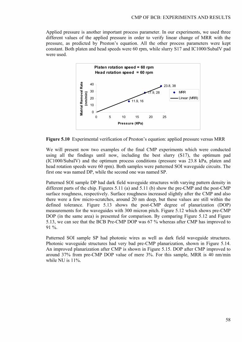
CMP OF BCB: EXPERIMENTS AND RESULTS
58
Applied pressure is another important process parameter. In our experiments, we used three different values of the applied pressure in order to verify linear change of MRR with the pressure, as predicted by Preston’s equation. All the other process parameters were kept constant. Both platen and head speeds were 60 rpm, while slurry S17 and IC1000/SubaIV pad were used.
Platen rotation speed = 60 rpm Head rotation speed = 60 rpm
11.9, 16
17.9, 28
23.8, 38
0
10
20
30
40
0 5 10 15 20 25
Pressure (KPa)
Mat
rial R
emov
al R
ate
(nm
/min
) MRR
Linear (MRR)
Figure 5.10 Experimental verification of Preston’s equation: applied pressure versus MRR
We will present now two examples of the final CMP experiments which were conducted using all the findings until now, including the best slurry (S17), the optimum pad (IC1000/SubaIV) and the optimum process conditions (pressure was 23.8 kPa, platen and head rotation speeds were 60 rpm). Both samples were patterned SOI waveguide circuits. The first one was named DP, while the second one was named SP.
Patterned SOI sample DP had dark field waveguide structures with varying pattern density in different parts of the chip. Figures 5.11 (a) and 5.11 (b) show the pre-CMP and the post-CMP surface roughness, respectively. Surface roughness increased slightly after the CMP and also there were a few micro-scratches, around 20 nm deep, but these values are still within the defined tolerance. Figure 5.13 shows the post-CMP degree of planarization (DOP) measurements for the waveguides with 300 micron pitch. Figure 5.12 which shows pre-CMP DOP (in the same area) is presented for comparison. By comparing Figure 5.12 and Figure 5.13, we can see that the BCB Pre-CMP DOP was 67 % whereas after CMP has improved to 91 %.
Patterned SOI sample SP had photonic wires as well as dark field waveguide structures. Photonic waveguide structures had very bad pre-CMP planarization, shown in Figure 5.14. An improved planarization after CMP is shown in Figure 5.15. DOP after CMP improved to around 37% from pre-CMP DOP value of mere 3%. For this sample, MRR is 40 nm/min while NU is 11%.
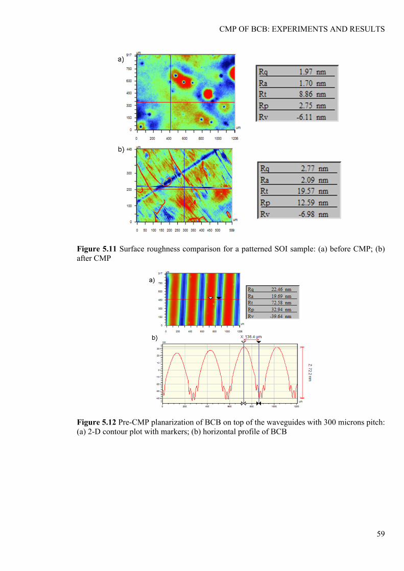
CMP OF BCB: EXPERIMENTS AND RESULTS
59
Figure 5.11 Surface roughness comparison for a patterned SOI sample: (a) before CMP; (b) after CMP
Figure 5.12 Pre-CMP planarization of BCB on top of the waveguides with 300 microns pitch: (a) 2-D contour plot with markers; (b) horizontal profile of BCB

CMP OF BCB: EXPERIMENTS AND RESULTS
60
Figure 5.13 Post-CMP planarization of BCB on top of the waveguides with 300 microns pitch: (a) 2-D contour plot with markers; (b) horizontal profile of BCB
Figure 5.14 Pre-CMP photonic wire waveguide structure planarization: (a) 3D view; (b) 2D view with markers; (c) BCB x-axis profile; (d) BCB y-axis profile.
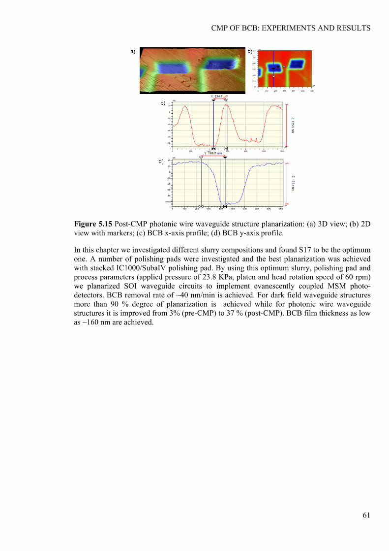
CMP OF BCB: EXPERIMENTS AND RESULTS
61
Figure 5.15 Post-CMP photonic wire waveguide structure planarization: (a) 3D view; (b) 2D view with markers; (c) BCB x-axis profile; (d) BCB y-axis profile.
In this chapter we investigated different slurry compositions and found S17 to be the optimum one. A number of polishing pads were investigated and the best planarization was achieved with stacked IC1000/SubaIV polishing pad. By using this optimum slurry, polishing pad and process parameters (applied pressure of 23.8 KPa, platen and head rotation speed of 60 rpm) we planarized SOI waveguide circuits to implement evanescently coupled MSM photo-detectors. BCB removal rate of ~40 nm/min is achieved. For dark field waveguide structures more than 90 % degree of planarization is achieved while for photonic wire waveguide structures it is improved from 3% (pre-CMP) to 37 % (post-CMP). BCB film thickness as low as ~160 nm are achieved.
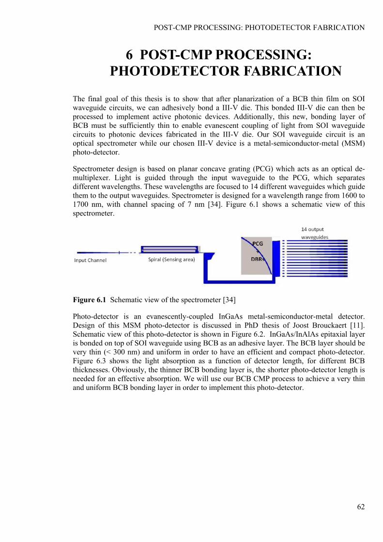
POST-CMP PROCESSING: PHOTODETECTOR FABRICATION
62
6 POST-CMP PROCESSING: PHOTODETECTOR FABRICATION
The final goal of this thesis is to show that after planarization of a BCB thin film on SOI waveguide circuits, we can adhesively bond a III-V die. This bonded III-V die can then be processed to implement active photonic devices. Additionally, this new, bonding layer of BCB must be sufficiently thin to enable evanescent coupling of light from SOI waveguide circuits to photonic devices fabricated in the III-V die. Our SOI waveguide circuit is an optical spectrometer while our chosen III-V device is a metal-semiconductor-metal (MSM) photo-detector.
Spectrometer design is based on planar concave grating (PCG) which acts as an optical de-multiplexer. Light is guided through the input waveguide to the PCG, which separates different wavelengths. These wavelengths are focused to 14 different waveguides which guide them to the output waveguides. Spectrometer is designed for a wavelength range from 1600 to 1700 nm, with channel spacing of 7 nm [34]. Figure 6.1 shows a schematic view of this spectrometer.
Figure 6.1 Schematic view of the spectrometer [34]
Photo-detector is an evanescently-coupled InGaAs metal-semiconductor-metal detector. Design of this MSM photo-detector is discussed in PhD thesis of Joost Brouckaert [11]. Schematic view of this photo-detector is shown in Figure 6.2. InGaAs/InAlAs epitaxial layer is bonded on top of SOI waveguide using BCB as an adhesive layer. The BCB layer should be very thin (< 300 nm) and uniform in order to have an efficient and compact photo-detector. Figure 6.3 shows the light absorption as a function of detector length, for different BCB thicknesses. Obviously, the thinner BCB bonding layer is, the shorter photo-detector length is needed for an effective absorption. We will use our BCB CMP process to achieve a very thin and uniform BCB bonding layer in order to implement this photo-detector.
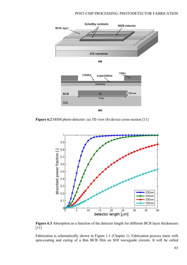
POST-CMP PROCESSING: PHOTODETECTOR FABRICATION
63
Figure 6.2 MSM photo-detector: (a) 3D view (b) device cross-section [11]
Figure 6.3 Absorption as a function of the detector length for different BCB layer thicknesses [11]
Fabrication is schematically shown in Figure 1.1 (Chapter 1). Fabrication process starts with spin-coating and curing of a thin BCB film on SOI waveguide circuits. It will be called
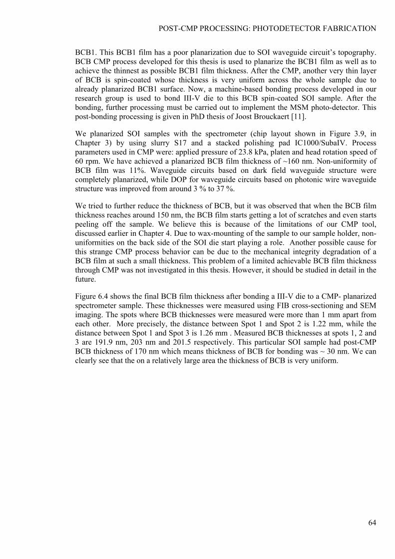
POST-CMP PROCESSING: PHOTODETECTOR FABRICATION
64
BCB1. This BCB1 film has a poor planarization due to SOI waveguide circuit’s topography. BCB CMP process developed for this thesis is used to planarize the BCB1 film as well as to achieve the thinnest as possible BCB1 film thickness. After the CMP, another very thin layer of BCB is spin-coated whose thickness is very uniform across the whole sample due to already planarized BCB1 surface. Now, a machine-based bonding process developed in our research group is used to bond III-V die to this BCB spin-coated SOI sample. After the bonding, further processing must be carried out to implement the MSM photo-detector. This post-bonding processing is given in PhD thesis of Joost Brouckaert [11].
We planarized SOI samples with the spectrometer (chip layout shown in Figure 3.9, in Chapter 3) by using slurry S17 and a stacked polishing pad IC1000/SubaIV. Process parameters used in CMP were: applied pressure of 23.8 kPa, platen and head rotation speed of 60 rpm. We have achieved a planarized BCB film thickness of ~160 nm. Non-uniformity of BCB film was 11%. Waveguide circuits based on dark field waveguide structure were completely planarized, while DOP for waveguide circuits based on photonic wire waveguide structure was improved from around 3 % to 37 %.
We tried to further reduce the thickness of BCB, but it was observed that when the BCB film thickness reaches around 150 nm, the BCB film starts getting a lot of scratches and even starts peeling off the sample. We believe this is because of the limitations of our CMP tool, discussed earlier in Chapter 4. Due to wax-mounting of the sample to our sample holder, non-uniformities on the back side of the SOI die start playing a role. Another possible cause for this strange CMP process behavior can be due to the mechanical integrity degradation of a BCB film at such a small thickness. This problem of a limited achievable BCB film thickness through CMP was not investigated in this thesis. However, it should be studied in detail in the future.
Figure 6.4 shows the final BCB film thickness after bonding a III-V die to a CMP- planarized spectrometer sample. These thicknesses were measured using FIB cross-sectioning and SEM imaging. The spots where BCB thicknesses were measured were more than 1 mm apart from each other. More precisely, the distance between Spot 1 and Spot 2 is 1.22 mm, while the distance between Spot 1 and Spot 3 is 1.26 mm . Measured BCB thicknesses at spots 1, 2 and 3 are 191.9 nm, 203 nm and 201.5 respectively. This particular SOI sample had post-CMP BCB thickness of 170 nm which means thickness of BCB for bonding was ~ 30 nm. We can clearly see that the on a relatively large area the thickness of BCB is very uniform.
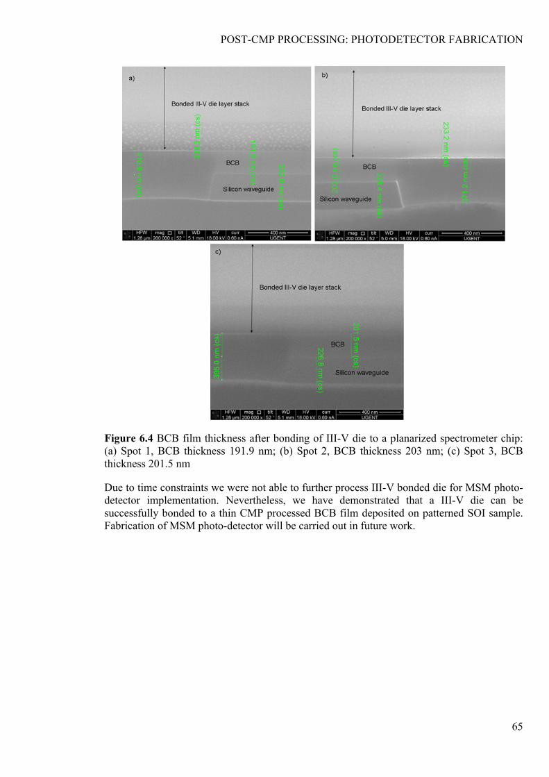
POST-CMP PROCESSING: PHOTODETECTOR FABRICATION
65
Figure 6.4 BCB film thickness after bonding of III-V die to a planarized spectrometer chip: (a) Spot 1, BCB thickness 191.9 nm; (b) Spot 2, BCB thickness 203 nm; (c) Spot 3, BCB thickness 201.5 nm
Due to time constraints we were not able to further process III-V bonded die for MSM photo-detector implementation. Nevertheless, we have demonstrated that a III-V die can be successfully bonded to a thin CMP processed BCB film deposited on patterned SOI sample. Fabrication of MSM photo-detector will be carried out in future work.
CONCLUSIONS AND PROSPECTS FOR FUTURE WORK
66
7 CONCLUSIONS AND PROSPECTS FOR FUTURE WORK
7.1 Conclusions Chemical mechanical planarization process for BCB was developed in this study. Effect of the BCB curing profile on planarization of BCB was investigated and it was found that a slow temperature ramp-up during the pre-curing stage improves the degree of planarization. It was also found that using a relatively low temperature (100oC) for BCB bake, after the spin-coating, substantially reduces defects in a BCB film.
Several slurry compositions were studied and the slurry combination of SPM commercial slurry, hydrogen peroxide, Triton X-100, cupric nitrate and citric acid was found to be the best. BCB removal rate of 40 nm/min was achieved using this slurry composition. It was also found that addition of ethylene glycol to this slurry reduces the removal rate as well as surface roughness of a BCB film.
Different polishing pads were also investigated. We found that slurry transport ability of a pad is very important for a uniform removal rate of thin BCB films. Stacked pad, in which a very hard pad is put on top of a soft pad, gave the best planarization performance. Concentric groove pattern on the stacked pad improved slurry transport ability and very uniform removal rate of BCB was achieved.
Experiments with different CMP process parameters were conducted and finally, using the optimized values of applied pressure, platen rotation speed and head rotation speed, a number of patterned SOI samples were planarized, reducing the BCB thickness down to ~160 nm. In the end, a successful adhesive bonding of III-V die to the CMP-processed BCB film was demonstrated. Total thickness of BCB achieved after bonding was ~200 nm. This particular SOI sample had post-CMP BCB thickness of 170 nm which means thickness of BCB for bonding was ~ 30 nm.
7.2 Prospects for Future Work 1. Problem regarding the defects in a BCB film before CMP should be studied in more
detail.
2. Although a very good slurry composition was found, the relative amount of different slurry components should be studied in more detail to further improve removal rate and post-CMP surface smoothness. One recommendation is to reduce the proportion of Triton X-100 in the slurry and further studies should be focused in this direction.
3. Due to time constraints, CMP process parameters were not studied in detail and this remains to be investigated more carefully. Especially, the effect of slurry flow rate on CMP output variables should be thoroughly investigated.
4. A CMP tool with more advanced carrier head design should be used to investigate the process parameters, especially the edge effect.

CONCLUSIONS AND PROSPECTS FOR FUTURE WORK
67
5. Diamond conditiong should be included in BCB CMP process to achieve sample to sample uniformity.
6. It should be studied in detail why BCB film is damaged and peels off during CMP, when its thickness reaches 150 nm. Solving this problem is essential in order to achieve even thinner planarized BCB layers, suitable for fabrication of evanescently-coupled photonic devices based on hybrid integration.
7. Post-CMP cleaning procedure should be developed in order to remove slurry residues and other debris from the polished BCB film.

68
REFERENCES
[1] S. Lombardo, S. Campisano, G. Vandenhoven, A. Cacciato, and A. Polman “A Room- temperature Luminescence from Er3+-implanted semi-insulating polycrystalline silicon,” Appl. Phys. Lett., vol. 63, pp 1942–1944, 1993.
[2] L. Pavesi, L. Dal Negro, C. Mazzoleni, G. Franzò, and F. Priolo, “Optical gain in silicon nanocrystals,” Nature, vol.408, pp. 440–444, 2000.
[3] O. Boyraz and B. Jalali, “Demonstration of a silicon Raman laser,” Opt. Express, vol. 12, p.5269, 2004.
[4] H. S. Rong, R. Jones, A. S. Liu, O. Cohen, D. Hak, A. Fang, M. J. Paniccia, “A continuous wave Raman silicon laser,” Nature, vol. 433, pp. 725-728, 2005.
[5] Sebastian Lourdudoss, Fredrik Olsson, and Yanting Sun “Novel routes in heteroepitaxy and selective area growth for Nanophotonics”, Proc. of SPIE Vol. 6900, 69000H, (2008).
[6] A.W. Fang et al., "A Continuous-Wave Hybrid AlGaInAs–Silicon Evanescent Laser", IEEE Photonics Technology Letters, vol. 18, no. 18, pp. 1143-1145, 2006.
[7] Hsu-Hao Chang et al., "1310nm silicon evanescent laser", Optics Express, vol. 15, no. 18, pp. 11466-11470, 2007.
[8] A.W. Fang et al., "A Distributed Bragg Reflector Silicon Evanescent Laser", in Proceedings of Group IV Photonics Conference, Sorento, Italy, Sept. 2008, pp. 58-60.
[9] A. W. Fang, et al., “A distributed feedback silicon evanescent laser,” Opt. Express, vol 16, pp. 4413-4419, 2008.
[10] Gunther Roelkens, “Heterogeneous III-V/Silicon Photonics:Bonding Technology and Integrated Devices” PhD thesis, University of Ghent, 2006.
[11] Joost Brouckaert, “Heterogeneous integration of photodetectors on silicon photonic IC’s”, PhD thesis, University of Ghent (to be published).
[12] Wolters P. Available at http://www. peter-wolters.com/cmp/cmpmultilevel.htm
[13] Steigerwald JM, Murarka SP, Gutmann RJ, “Chemical Mechanical Planarization of Microelectronic Materials”, New York: Wiley; 1996.
[14] Oliver MR, editor, “Chemical–Mechanical Planarization of Semiconductor Materials”, Springer; 2004.
[15] Prof. Marc Heyns and Prof. Roger De Keersmaecker , “Chemical mechanical planarization (CMP)”, lecture notes IMEC (2009).
[16] F. Preston, J. SOC. Glass Tech. 11, 214 (1927).

69
[17] N.J Brown, P.C. Baker, and R.T. Maney, Proc. SPIE 306, 42 (1981).
[18] S. Sivaram, K. Monnig, R. Tolles, A. Maw, and R. Leggett, Proc, “3rd Int. Symposium on ULSI Science and Technology”, eds J.M. Andrews and G.K. Celler, The Electrochemical Society, Inc., Pennington, NJ (1991), p.606.
[19] Ungyu Paik,Jea-Gun Park, “Nanoparticle Engineering for Chemical-Mechanical Planarization” - Fabrication of Next-Generation Nanodevices, 2009. CMP Book Nanoparticle Engineering 2009.
[20] Shin Hwalirobert O. Miller, “Chemical Mechanical Polishing in Silicon Processing”, Volume 63. Academic Press, 2000.
[21] J. Coppeta, J. Rogers, A. Philipossian, F. Kaufman, “Characterizing Slurry Flow During CMP Using Laser Induced Fluorescence,” Second International CMP for ULSI Multilevel Interconnection Conference, Santa Clara, CA, pp. 307-314, Feb. 13- 14, 1997.
[22] Muldowney GP, James DB, “Characterization of CMP pad surface texture and pad–wafer contact”, Mater Res Soc Symp Proc 2004;816:K5.2.1–K5.2.12.
[23] Zantye PB, Kumar A, Sikder AK, “Chemical mechanical planarization for microelectronics applications”, Mater Sci Eng (R) 2004;45:89–220.
[24] http://www.azom.com/details.asp?ArticleID=935.
[25] Basim GB, Vakarelski IU, Moudgil B, “Role of interaction forces in controlling the stability and polishing performance of CMP slurries”, J Coll Interface Sci 2003;263:506–515.
[26] M. E. Mills, P. Townsend, D. Castillo, S. Martin, and A. Achen, “ Benzocyclobutene (DVS-BCB) polymer as an interlayer dielectric (ILD) material”, Microelectronic Engineering, 33(1-4):327–334, 1997.
[27] P. E. Garrou, R. H. Heistand, M. G. Dibbs, T. A. Mainal, C. E. Mohler, T. M. Stokich, P. H. Townsend, G. M. Adema, M. J. Berry, and I. Turlik, “Rapid Thermal Curing of BCB Dielectric”, IEEE Transactions on Components Hybrids and Manufacturing Technology, 16(1):46–52, 1993.
[28] Y. H. So, P. E. Garrou, J. H. Im, and K. Ohba, “Benzocyclobutenebased polymers for microelectronic applications”, Polymers for Microelectronics and Nanoelectronics, 874:279–293, 2004.
[29] J. H. Im, E. O. Shaffer, T. Stokich, A. Strandjord, J. Hetzner, J. Curphy, C. Karas, G. Meyers, D. Hawn, A. Chakrabarti, and S. Froelicher, “ On the mechanical reliability of photo-BCB-based thin film dielectric polymer for electronic packaging applications”, Journal of Electronic Packaging, 122(1):28–33, 2000.
[30] W. Verhaverbeke and F. Parker, “The Role of H2O2- in SC1 Cleaning Solutions”, In Mater. Res. Soc. Symp. Proc. Science and Technology of Semiconductor Surface Preparation, volume 477, 2007.
[31] Dow Chemicals website (http://www.dow.com/cyclotene/): Cyclotene: BCB processing.
70
[32] McMahon JJ, Niklaus F, Kumar RJ, Yu J, Lu J-Q, Gutmann RJ (2005), “CMP Compatibility of partially cured benzocyclobutene (BCB) for a via-first 3D IC process”, In: Kumar A, Lee JA, Obeng YS, Vos I, Johns EC (eds) Chemical-Mechanical Planarization—Integration, Technology and Reliability, MRS Proc vol 867: pp W4.4.1-6.
[33] Jan. M. Neirynck, S. P. Murarka and R. J. Gutmann, “Investigations of the chemical-mechanical polishing of polymer films for ILD applications” Mat. Res. Soc. Symp. Proc. Vol. 381 (1995).
[34] Alvaro Casas Bedoya, “Design and fabrication of a miniature spectrometer-on-a-chip for Biodiesel sensing applications”, Masters thesis, University of Ghent, 2009.
[35] M. D. Bullwinkel, J. Gu, G. A. Campbell, and P. C. Sukanek, “The Effect of polymer molecular-weight and solvent-type on the planarization of spin-coated films”, Journal of the Electrochemical Society, 142(7):2389–2394, 1995.
[36] Parshuram B. Zantye, Ashok Kumar, A.K. Sikder, “Chemical mechanical planarization for microelectronics applications”, Materials Science and Engineering R 45 (2004) 89–220.
[37] http://www.avsusergroups.org/tfug_pdfs/TFUG_10_2002_Burke.pdf.
[38] Jan. M. Neirynck, S. P. Murarka and R. J. Gutmann, “Investigations of the chemical-mechanical polishing of polymer films for ILD applications” Mat. Res. Soc. Symp. Proc. Vol. 381 (1995).
[39] Jan M, Neirynck, G.-R, Yang, Shyam P, Murarka, Ronald J. Gutmann,”The addition of surfactant to slurry for polymer CMP: effects on polymer surface, removal rate and underlying Cu”, Thin Solid Films 290-291 (1996) 447-452.
[40] G.-R. Yang, Y.-P. Zhao, Jan M. Neirynck, Snyam P.M urarka, and Ronald J. Gutmann,”Chemical-Mechanical Polishing of Parylene N and Benzocyclobutene Films”, J. Electrochem. Soc., Vol. 144, No. 9, September 1997.
[41] S.P. Murarka, “Chemical-mechanical planarization of the polymer interlayer dielectrics”, Mat. Res. Soc. Symp. Proc. Vol. 511 (1998)
[42] Christopher L. Borst, Dipto G. Thakurta, William N. Gill, Ronald J. Gutmann, “Chemical Mechanical Polishing Mechanisms of Low Dielectric Constant Polymers in Copper Slurries”, Journal of The Electrochemical Society, 146 (11) 4309-4315 (1999).
[43] J. J. McMahon, F. Niklaus, R. J. Kumar, J. Yu, J.-Q. Lu, and R. J. Gutmann,” CMP Compatibility of Partially Cured Benzocyclobutene (BCB) for a Via-First 3D IC Process”, Mater. Res. Soc. Symp. Proc. Vol. 867 ( 2005).
[44] Alireza Modafe, Nima Ghalichechian, Michael Powers, Michael Khbeis, Reza Ghodssi, “Embedded benzocyclobutene in silicon: An integrated fabrication process for electrical and thermal isolation in MEMS”, Microelectronic Engineering 82 (2005) 154 167.
[45] Fei Geng, Xiao-yun Ding, Gao-wei Xu and Le Luo, “A wafer-scale packaging structure with monolithic microwave integrated circuits and passives embedded in a silicon substrate for multichip modules for radio frequency applications”, J. Micromech. Microeng. 19 (2009) 105011.

71
[46] Geng Fei, Ding Xiaoyun, Xu Gaowei, and Luo Le, “A wafer-level 3D packaging structure with Benzocyclobutene as a dielectric for multichip module fabrication”, Journal of Semiconductors. Vol. 30, No. 10, October (2009).
[47] J. Warnock, J. Electrochem. SOC1. 38, 2398 (1991).
[48] http://www.machinist-materials.com/hardness.htm
[49] US patent no.US6270395
[50] US patent no.US6830503
[51] Edited by Yuzhuo Li “Microelectronic Application of Chemical Mechanical Planarization”, Wiley-Interscience, 2008s