Characterization of Transistor Matching in Silicon-Germanium
56
Characterization of Transistor Matching in Silicon-Germanium Heterojunction Bipolar Transistors A Thesis Presented to The Academic Faculty by Mustansir M. Pratapgarhwala In Partial Fulfillment of the Requirements for the Degree Master of Science in School of Electrical and Computer Engineering Georgia Institute of Technology December 2005
Transcript of Characterization of Transistor Matching in Silicon-Germanium
Characterization of Transistor Matching inSilicon-Germanium Heterojunction Bipolar Transistors
A ThesisPresented to
The Academic Faculty
by
Mustansir M. Pratapgarhwala
In Partial Fulfillmentof the Requirements for the Degree
Master of Sciencein School of Electrical and Computer Engineering
Georgia Institute of TechnologyDecember 2005

Characterization of Transistor Matching inSilicon-Germanium Heterojunction Bipolar Transistors
Approved by:
Professor John D. Cressler, AdvisorSchool of Electrical and Computer EngineeringGeorgia Institute of Technology
Professor Joy LaskarSchool of Electrical and Computer EngineeringGeorgia Institute of Technology
Professor John PapapolymerouSchool of Electrical and Computer EngineeringGeorgia Institute of Technology
Date Approved: November 21, 2005

ACKNOWLEDGEMENTS
I am deeply indebted to Dr. John D. Cressler for his patience, guidance, and support
throughout my master’s program. My inspiration came from his passion for research
and his confidence in my abilities. Working under his leadership in such an exciting field
was both educationally and professionally enriching. I would also like to thank the other
members of my thesis advisory committee, Dr. Joy Laskar and Dr. John Papapolymerou.
I would also like to extend a special thanks to Jon Comeau for his guidance that helped
enhance my understanding of this field. I would also like to thank Akil Sutton, Becca
Haugerud, Adnan Ahmed, Ramkumar Krithivasan, and A.P. Gnana Prakash for all their
assistance in the completion of this work.
I am grateful to the National Semiconductor SiGe team for their useful insight and
for providing wafers used in these studies. I would also like to thank the following for
supporting this work: BAE Systems, DTRA under the Radiation Hardened Microelectronics
Program, NASA-GSFC under the Electronics Radiation Characterization Program, DARPA,
and the Georgia Electronic Design Center at Georgia Tech. The assistance of Paul Marshall,
Cheryl Marshall, and Ray Ladbury made the radiation experiments possible and is greatly
appreciated.
Finally, I would like to thank my family and friends for their support, encouragement,
and understanding throughout my master’s research
iii

TABLE OF CONTENTS
ACKNOWLEDGEMENTS . . . . . . . . . . . . . . . . . . . . . . . . . . . . . . iii
LIST OF TABLES . . . . . . . . . . . . . . . . . . . . . . . . . . . . . . . . . . vi
LIST OF FIGURES . . . . . . . . . . . . . . . . . . . . . . . . . . . . . . . . . . vii
SUMMARY . . . . . . . . . . . . . . . . . . . . . . . . . . . . . . . . . . . . . . ix
I INTRODUCTION . . . . . . . . . . . . . . . . . . . . . . . . . . . . . . . . 1
1.1 Motivation . . . . . . . . . . . . . . . . . . . . . . . . . . . . . . . . . . 1
1.2 SiGe HBT BiCMOS Technology . . . . . . . . . . . . . . . . . . . . . . 2
1.3 SiGe Device Physics . . . . . . . . . . . . . . . . . . . . . . . . . . . . . 6
1.4 Summary . . . . . . . . . . . . . . . . . . . . . . . . . . . . . . . . . . . 11
II CHARACTERIZING MATCHING . . . . . . . . . . . . . . . . . . . . . . . 12
2.1 Introduction . . . . . . . . . . . . . . . . . . . . . . . . . . . . . . . . . 12
2.2 Matching Concepts . . . . . . . . . . . . . . . . . . . . . . . . . . . . . 12
2.2.1 MOS Devices . . . . . . . . . . . . . . . . . . . . . . . . . . . . 13
2.2.2 Bipolar Devices . . . . . . . . . . . . . . . . . . . . . . . . . . . 15
2.3 Mismatch Measurements . . . . . . . . . . . . . . . . . . . . . . . . . . 15
2.3.1 Design of Test Structures . . . . . . . . . . . . . . . . . . . . . . 15
2.3.2 Results . . . . . . . . . . . . . . . . . . . . . . . . . . . . . . . . 16
2.3.3 Summary . . . . . . . . . . . . . . . . . . . . . . . . . . . . . . 18
III RADIATION EFFECTS . . . . . . . . . . . . . . . . . . . . . . . . . . . . . 22
3.1 Introduction . . . . . . . . . . . . . . . . . . . . . . . . . . . . . . . . . 22
3.2 Radiation Concepts and Damage Mechanisms . . . . . . . . . . . . . . . 22
3.3 Radiation Effects in SiGe HBTs . . . . . . . . . . . . . . . . . . . . . . . 26
3.3.1 dc Results . . . . . . . . . . . . . . . . . . . . . . . . . . . . . . 27
3.3.2 Summary . . . . . . . . . . . . . . . . . . . . . . . . . . . . . . 29
iv

IV TEMPERATURE MISMATCH EFFECTS . . . . . . . . . . . . . . . . . . 34
4.1 Introduction . . . . . . . . . . . . . . . . . . . . . . . . . . . . . . . . . 34
4.2 High Temperature Concepts . . . . . . . . . . . . . . . . . . . . . . . . . 34
4.3 Temperature Effects . . . . . . . . . . . . . . . . . . . . . . . . . . . . . 38
4.3.1 Results . . . . . . . . . . . . . . . . . . . . . . . . . . . . . . . . 38
4.3.2 Summary . . . . . . . . . . . . . . . . . . . . . . . . . . . . . . 41
V CONCLUSION . . . . . . . . . . . . . . . . . . . . . . . . . . . . . . . . . . 42
5.1 Conclusion . . . . . . . . . . . . . . . . . . . . . . . . . . . . . . . . . . 42
5.2 Future Directions . . . . . . . . . . . . . . . . . . . . . . . . . . . . . . 43
REFERENCES . . . . . . . . . . . . . . . . . . . . . . . . . . . . . . . . . . . . . 44
v

LIST OF TABLES
1 Target device parameters for National SiGe BiCMOS technology. . . . . . . . 6
2 Matched-Pair Device Geometries Investigated. . . . . . . . . . . . . . . . . . . 16
vi

LIST OF FIGURES
1 A schematic cross-section of the SiGe HBT. . . . . . . . . . . . . . . . . . . . 3
2 Representative SIMS profile for a first generation SiGe HBT. . . . . . . . . . . 4
3 A schematic device cross-section of the National BiCMOS8 SiGe HBT underinvestigation. . . . . . . . . . . . . . . . . . . . . . . . . . . . . . . . . . . . 5
4 SEM device cross-section of the National BiCMOS8 SiGe HBT under investigation. 5
5 Energy band diagram for a graded base SiGe HBT and a Si BJT. . . . . . . . . 7
6 Representative Gummel plot for a SiGe HBT as compared to a Si BJT. . . . . . 9
7 (a) Circuit representation of the matching structures;(b) Device geometry available. 17
8 Forward-mode Gummel characteristics. . . . . . . . . . . . . . . . . . . . . . 18
9 Current gain. . . . . . . . . . . . . . . . . . . . . . . . . . . . . . . . . . . . 19
10 Collector current variation as a function of emitter-base bias for a variety ofdevice geometries. . . . . . . . . . . . . . . . . . . . . . . . . . . . . . . . . 20
11 Collector current variation histogram. . . . . . . . . . . . . . . . . . . . . . . 20
12 Standard deviation of the collector current variation as a function of the reciprocalof the square root of the area. . . . . . . . . . . . . . . . . . . . . . . . . . . . 21
13 Illustration of the solar wind and radiation belts surrounding the Earth. . . . . . 24
14 Forward-mode Gummel characteristics before and after irradiation. . . . . . . . 28
15 Current gain degradation before and after irradiation. . . . . . . . . . . . . . . 29
16 Collector current variation as a function of emitter-base bias for a variety ofdevice geometries. . . . . . . . . . . . . . . . . . . . . . . . . . . . . . . . . 30
17 Collector current variation histogram - post-radiation. . . . . . . . . . . . . . . 30
18 Standard deviation of the collector current variation as a function of the reciprocalof the square root of the area. . . . . . . . . . . . . . . . . . . . . . . . . . . . 31
19 Collector currents for each transistor of the matched pair for both pre-radiationand post-radiation. . . . . . . . . . . . . . . . . . . . . . . . . . . . . . . . . 32
20 Correlation of collector current variation between pre-radiation and post-radiation. 33
21 Energy band visualization of thermal generation processes. . . . . . . . . . . . 36
22 Forward-mode Gummel characteristics as a function of temperature. . . . . . . 38
23 Current gain as a function of collector current at 25C, 50 C, 75 C, and 100C. . . 39
vii

24 Standard deviation of the collector current variation as a function of temperature. 40
viii

SUMMARY
Device mismatch is crucial in many types of analog circuits, including differential
pairs for the input stages of amplifiers, current mirrors for biasing, and in various circuits
topologies utilizing integer multiples of identical components such as bandgap references,
ADCs, DACs, and filters. Thus, accurate transistor matching is at the very heart of robust
analog circuit design. Chapter II explores the fundamentals of device mismatch and explores
for the first time the geometric dependence of collector current variations in SiGe HBTs.
Chapter III examined the effects of radiation on various SiGe HBT BiCMOS technologies.
The space community is increasingly using COTS parts in spaceborne systems, thus radiation
testing on new commercial technologies is imperative. The effects of proton irradiation on
matched device pairs on a new commercially-available SiGe technology were examined for
the first time. Chapter IV presents the results of the effects of collector current mismatch at
high temperatures. As such, device mismatch effects at high-temperature have not been
seriously studied. This is probably because the temperature effects are believed to be
insignificant to transistor mismatch. This characteristic is essential in order to prove its
applicability in high-temperature precision analog circuits.
ix

CHAPTER I
INTRODUCTION
1.1 Motivation
In today’s fast growing markets, analog and digital signal processing (DSP) are the key
technologies fueling innovative, high-growth applications. Such applications include digital
wireless, broadband access, digital audio, high-resolution imaging and motor control. As
the interface between digital and "real-world" signals, analog chips play an integral role
in most electronic equipment. For example, depending on the system, for every DSP in
an electronic system, there are approximately ten analog components. As a result, analog
technology is an engine driving the Information age with high-growth applications such as
wireless and broadband communications, consumer audio and video, and PC peripherals.
Due to the broad spectrum of analog applications, the analog IC market is a highly
fragmented and competitive sector of the semiconductor industry. The Semiconductor
Industry Association (SIA) estimated the analog market at $31.3 billion in 2004 and forecasts
it to grow to $33.7 billion in 2006. This growth pattern fuelled by the increasing need for
high-performance analog in digital systems has led to increase in complexity and capability
of analog ICs. In order, to accommodate the accelerating need for faster and cheaper DSP,
high performance and cost effective analog ICs will be required. This task places new
requirements on technology, and poses new challenges for technologists.
Due to the rapid expansion of the analog IC market, technologists venture towards
higher performance devices while maintaining lower costs. Traditionally, analog circuits
required much higher power supply levels [3]. This deemed Sige HBTs unsuitable since
high BVCEO came at a cost of poor high frequency performance. However, due to declining
analog voltage levels, SiGe has developed a niche in the analog IC market. This technology
1

provides low power, low noise, and high frequency analog solutions in comparison to Si-
only technology [2]. With aggressive design efforts and shrinking device sizes, parasitics
such as device mismatch limit circuit performance.
In general, transistor "mismatch" refers to the measurable differences in electrical characteristics
(e.g., IC , β, or gm) between two identically designed and layed-out devices, which are
biased identically, and placed in very close proximity on the wafer to minimize cross-wafer
process variations (this is often called a "matched pair"). Matched pairs are critical in
many types of analog circuits, including differential pairs for the input stages of amplifiers,
current mirrors for biasing, and in various circuits topologies utilizing integer multiples of
identical components such as bandgap references, ADCs, DACs, and filters. Thus, accurate
transistor matching is at the very heart of robust analog circuit design.
The primary goal of this thesis will be to investigate the transistor level static performance
implications of device mismatch of SiGe HBT BiCMOS technology. We will try to achieve
this goal by presenting and analyzing the dc characterization results of various device
geometries under extreme conditions such as radiation and a range of temperatures.
1.2 SiGe HBT BiCMOS Technology
Silicon-Germanium (SiGe) heterojunction bipolar transistor (HBT) technology uses Si-
based bandgap engineering to provide high speed, low noise, and power efficient devices in
a high-yielding, low cost IC platform. SiGe BiCMOS technology offers high-performance
SiGe HBTs and passive component capabilities combined with deep sub-micron CMOS.
The SiGe HBT uses bandgap engineering to achieve III-V like performance while maintaining
compatibility with conventional Si CMOS manufacturing. This technology allows for
system-on-a-chip (SoC) integration. As a result, SiGe technology is rapidly becoming a
popular choice for analog, digital, radio frequency (RF), microwave, and millimeter wave
integrated circuit applications.
Silicon-Germanium (SiGe) is a new technology that combines the integration and cost
2

Figure 1: A schematic cross-section of the SiGe HBT.
benefits of silicon with the speed of more esoteric and expensive technologies such as
gallium-arsenide. The key difference between SiGe HBTs and Si BJTs is the introduction
of SiGe epi layer into the base of an otherwise all-silicon bipolar transistor. The base region
is thus comprised of a Si buffer, boron-doped graded SiGe alloy active layer, and a Si cap.
Figure 2 depicts a SIMS doping and Ge profile for a representative first generation SiGe
HBT.
The inclusion of graded SiGe alloy in the base facilitates bandgap engineering for use
in tailoring npn bipolar transistors. The compressive strain associated with SiGe alloy
produces an additional bandgap shrinkage which improves carrier mobility in comparison
to Si BJTs. This leads to lower base resistance and improved dynamic response [1].
The trade-off in SiGe epitaxial growth involves balancing of two competing temperature
dependent requirements, namely, mobility of the adhering atomic species and formation
of dislocation nucleation. As for increased mobility, large temperatures are preferred,
but to avoid strain relaxation by enhanced dislocation formation, low temperatures are
necessary. Several techniques have been developed for the growth of SiGe epitaxial films.
The list includes MBE, [34] and [35], limited Reaction Processing (LRP) or Rapid thermal
Chemical Vapor Deposition (RTCVD) [36], Atmospherice Pressure Chemical Vapor Deposition
3

Figure 2: Representative SIMS profile for a first generation SiGe HBT.
(APCVD) [37], and ultra-high vacuum/chemical vapor deposition (UHV/CVD) [38]. The
UHV/CVD is a more widely used technique for SiGe epitaxial growth since it eliminates
the high thermal budget of conventional epitaxy by chemical means.
The SiGe BiCMOS technology under investigation is the commercially-available National
BiCMOS8 SiGe HBT process technology. The SiGe HBT utilizes deep trench isolation,
a self-aligned emitter-base structure, in-situ doped polysilicon emitter, and a non-selective
SiGe epitaxial base process. The process features six layers of metalization and includes
2.5V CMOS devices. The SiGe HBTs have a 0.4µm emitter stripe width, a nominal peak
fT of 60GHz, a peak fmax of 60-70GHz, and a BVCEO of 3.3V. A schematic cross-section
of the SiGe HBT is shown in Figure 1 and a SEM cross-section is depicted in Figure 4.
4
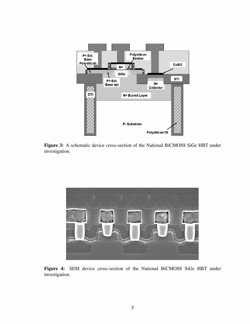
Figure 3: A schematic device cross-section of the National BiCMOS8 SiGe HBT underinvestigation.
Figure 4: SEM device cross-section of the National BiCMOS8 SiGe HBT underinvestigation.
5
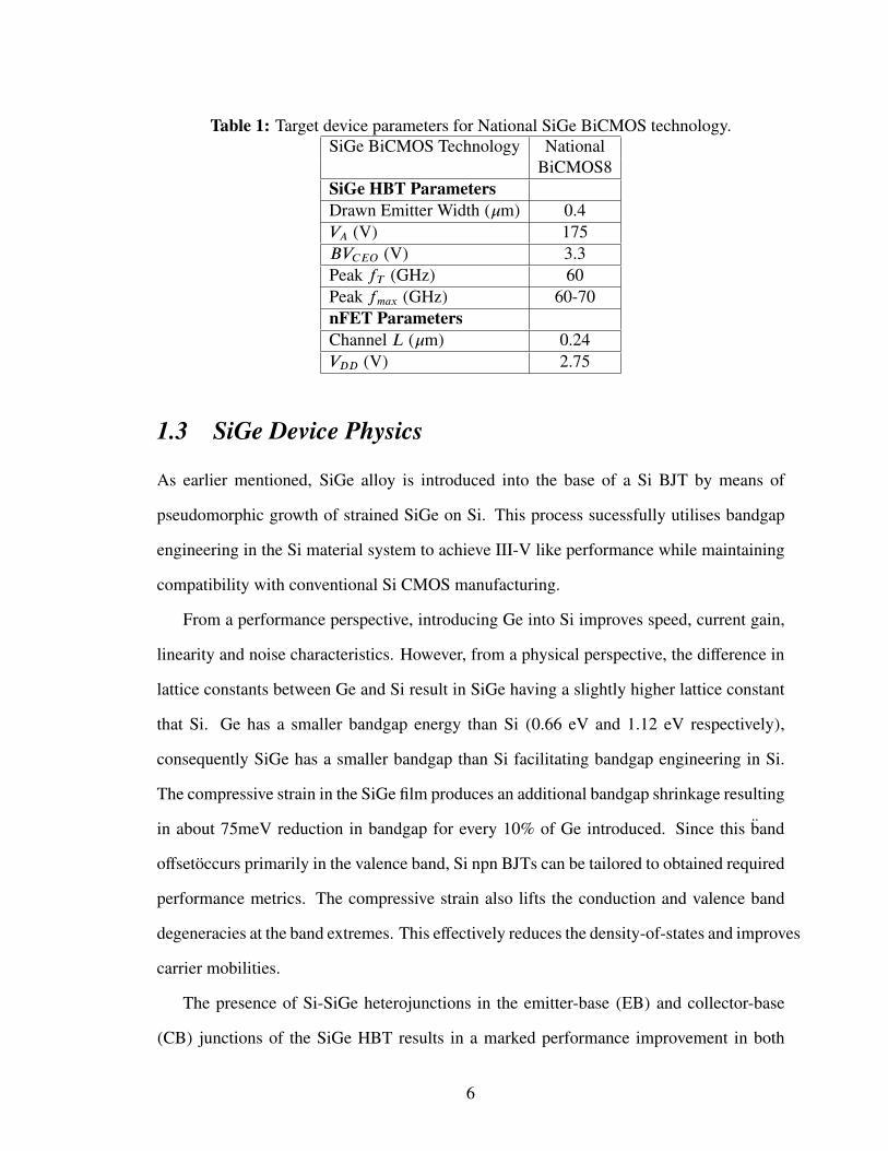
Table 1: Target device parameters for National SiGe BiCMOS technology.SiGe BiCMOS Technology National
BiCMOS8SiGe HBT ParametersDrawn Emitter Width (µm) 0.4VA (V) 175BVCEO (V) 3.3Peak fT (GHz) 60Peak fmax (GHz) 60-70nFET ParametersChannel L (µm) 0.24VDD (V) 2.75
1.3 SiGe Device Physics
As earlier mentioned, SiGe alloy is introduced into the base of a Si BJT by means of
pseudomorphic growth of strained SiGe on Si. This process sucessfully utilises bandgap
engineering in the Si material system to achieve III-V like performance while maintaining
compatibility with conventional Si CMOS manufacturing.
From a performance perspective, introducing Ge into Si improves speed, current gain,
linearity and noise characteristics. However, from a physical perspective, the difference in
lattice constants between Ge and Si result in SiGe having a slightly higher lattice constant
that Si. Ge has a smaller bandgap energy than Si (0.66 eV and 1.12 eV respectively),
consequently SiGe has a smaller bandgap than Si facilitating bandgap engineering in Si.
The compressive strain in the SiGe film produces an additional bandgap shrinkage resulting
in about 75meV reduction in bandgap for every 10% of Ge introduced. Since this band
offsetoccurs primarily in the valence band, Si npn BJTs can be tailored to obtained required
performance metrics. The compressive strain also lifts the conduction and valence band
degeneracies at the band extremes. This effectively reduces the density-of-states and improves
carrier mobilities.
The presence of Si-SiGe heterojunctions in the emitter-base (EB) and collector-base
(CB) junctions of the SiGe HBT results in a marked performance improvement in both
6
dc and ac characteristics over the Si BJT. The energy band diagram for a forward biased
graded-base SiGe HBT and a comparable Si BJT is shown in Figure 5. The effect of
graded Ge content in the base is apparent in the band structure changes shown above. A
slight reduction in the base bandgap at the EB junction (∆Eg,Ge(x = 0)) and a much larger
reduction at the CB junction (∆Eg,Ge(x = Wb)) is observed. This grading of Ge across the
base induces a built-in quasi-drift field (((∆Eg,Ge(x = Wb))-(∆Eg,Ge(x = 0)))/Wb) in the
neutral base region, positively impacting the minority carrier transport.
SiGeBase
p–Si
%Ge
� Eg,Ge(x=0) � Eg,Ge(x=Wb)
Emittern+ Si
Collectorn– Si
EC
EV
Si
SiGe
� Eg,Ge(grade)=� Eg,Ge(WB)– � Eg,Ge(0)
Figure 5: Energy band diagram for a graded base SiGe HBT and a Si BJT.
From Figure 5, we see that the emitter-base potential barrier is reduced in the SiGe
HBT with respect to the Si BJT, thereby allowing increased electron injection from emitter
to base. The enhanced electron injection leads to a higher collector current and current
gain. An expressions for the collector current density (JC ) can be derived in closed-form
7

from the generalized Moll-Ross JC relation [8],
JC =q(eqVBE/kT−1)
∫Wb
0pb(x)dx
Dnb(x)n2ib(x)
(1)
where Wb is the neutral base width for the applied bias VBE , pb(x) is the base doping, and
Dnb is the minority electron diffusivity in the base. The intrinsic carrier density in the SiGe
HBT is given by
n2ib = γn2
ioe∆Eapp
gb /kT e[∆Eg,Ge(grade)]x/(WbkT )e∆Eg,Ge(0)/kT (2)
where ∆Eapp
gb /kT is the apparent bandgap narrowing due to heavy doping in the base and
define ∆Eg,Ge(grade) as ∆Eg,Ge(Wb)−∆Eg,Ge(0). The low-doping intrinsic carrier density
for Si is n2io = NCNV e
−Ego/kT and γ = (NCNV )SiGe/(NCNV )Si < 1 is the effective density-
of-states ratio between SiGe and Si [23]. An expression for JC in a SiGe HBT can be
obtained using Equation 2 into 1[24], [25]:
JC,SiGe =qDnb
N−abWb
(
eqVBE/kT − 1)
n2ioe
∆Eappgb /kT
{
γηe∆Eg,Ge(0)/kT∆Eg,Ge(grade)/kT
1 − e−∆Eg,Ge(grade)/kT
}
(3)
where “∼” is a position-averaged quantity, N−ab is the ionized doping level in the base, and
η =(
˜Dnb
)
SiGe/(Dnb)Si > 1 is the minority electron diffusivity ratio between SiGe and Si.
Note the first term in Equation 3 corresponds to the Si BJT and the second term represents
the modification of JC due to the Ge content in the base. Figure 6 depicts the Gummel
characteristics for a typical SiGe HBT and a similarly constructed Si BJT. As expected, the
SiGe HBT exhibits higher collector current and approximately the same base current as the
Si BJT. The increase in JC for the SiGe HBT in turn leads to an increase in current gain
(β). The current gain ratio between a SiGe HBT and an identically constructed Si BJT can
be expressed as:
βSiGe
βSi∼=
JC,SiGe
JC,Si=
γη∆Eg,Ge(grade)/kTe∆Eg,Ge(0)/kT
1 − e−∆Eg,Ge(grade)/kT(4)
The current gain depends linearly on the band offset due to Ge grading across the base and
exponentially on the Ge induced band offset at the EB junction as Equation 4 indicates.
8

0.2 0.4 0.6 0.8 1.0
10–10
10–8
10–6
10–4
10–2
Base–Emitter Voltage (V)
Col
lect
or a
nd B
ase
Cur
rent
s (A
)
AE=0.5x2.5 m2 VCB=0
Silicon SiGe
Figure 6: Representative Gummel plot for a SiGe HBT as compared to a Si BJT.
Therefore, β is dependent on the Ge profile shape and can be modified for particular circuit
applications. The introduction of Ge in the base in effect decouples β from the base doping.
This fact implies that the base doping can be increased with out degrading β. Note that
higher base doping reduces the base resistance which has positive implications in terms of
frequency response and broadband noise.
The output conductance is an important design parameter for analog circuits and is
conveniently described by the Early voltage (VA). A graded Ge profile in the base of the
SiGe HBT leads to the enhancement of VA that of the Si BJT as shown below:
VA,SiGe
VA,Si
∣
∣
VBE = e∆Eg,Ge(grade)/kT
[
1 − e−∆Eg,Ge(grade)/kT
∆Eg,Ge(grade)/kT
]
(5)
The Early voltage depends exponentially on the Ge grading across the base, which decouples
VA from the base doping and hence β. Consequently a high “current-gain–Early voltage
product” (βVA product), a figure-of-merit for analog applications, can be maintained independent
9

of the base profile.βVA,SiGe
βVA,Si
= γηe∆Eg,Ge(0)/kT e∆Eg,Ge(grade)/kT (6)
Note that the βVA product for the SiGe HBT is enhanced over the Si BJT and is an
exponential function of the band offset at the EB junction as well the Ge grading across
the base.
Two important ac figures-of-merit are the unity-gain cutoff frequency (fT ) and the
maximum oscillation frequency (fmax). Both parameters are positively impacted by the
Ge content in the base as will be shown below. The unity-gain cutoff frequency is given by:
fT =1
2π
[
1gm
(Ceb + Ccb) + τb + τe +WCB
2vsat+ rcCcb
]−1
(7)
where gm is the intrinsic transconductance, Ceb and Ccb are the EB and CB depletion
capacitances, τb is the base transit time, τe is the emitter charge storage delay time, WCB
is the CB space-charge region width, vsat is the saturation velocity, and rc is the collector
resistance. The grading of Ge across the base induces a built-in electric field in the neutral
base region (directed from collector to emitter). This field accelerates the minority carriers
across the base which effectively reduces the base transit time.
τb,SiGe
τb,Si=
2η
kT
∆Eg,Ge(grade)
{
1 −kT
∆Eg,Ge(grade)
[
1 − e−∆Eg,Ge(grade)/kT ]}
(8)
Due to the inverse relationship between the emitter charge storage delay time and acβ, τe
is reduced for the SiGe HBT.
τe,SiGe
τe,Si'
JC,SiJC,SiGe
=1 − e−∆Eg,Ge(grade)/kT
γη∆Eg,Ge(grade)
kTe∆Eg,Ge(0)/kT
(9)
From Equation 7, it is clear that the reductions of both τb and τe will increase the fT of the
SiGe HBT over the Si BJT. The maximum oscillation frequency is given by:
fmax =
√
fT
8πCcbrb(10)
where rb is the ac base resistance and Ccb is the collector-base capacitance. The increase in
fT as well as a reduction in rb aid in improving the fmax of the SiGe HBT.
10

1.4 Summary
This chapter introdues the fabrication aspects and the device physics that govern the operation
of the SiGe HBT BiCMOS technology. The technology utilises bandgap engineering to
provide significant advantages over the Si BJT including increased β, VA, fT , and fmax.
Along with the high-performance SiGe HBTs, this technology provides passive component
capabilities combined with deep sub-micron CMOS for system-on-a-chip (SoC) integration.
In this thesis, Chapter II provides an understanding of device mismatch and its effects
on circuit performance. This chapter examines the geometric dependence of collector
current variation in SiGe HBTs. Chapter III of this thesis provides a general understanding
of the radiation concepts and terminology associated with radiation physics. The effect
of proton radiation on SiGe HBT technology is examined along with transistor mismatch
as a crucial design issue in space-borne precision analog circuits. Chapter IV explores the
dependence of device mismatch with respect to temperature. Chapter V presents conclusions
of the work presented in this thesis as well as suggestions for future directions for this
research.
11

CHAPTER II
CHARACTERIZING MATCHING
2.1 Introduction
Random device mismatch plays a key role in designing precision analog circuits. In general,
transistor "mismatch" refers to the measurable differences in electrical characteristics (e.g.,
IC , β, or gm) between two identically designed and layed-out devices, which are biased
identically, and placed in very close proximity on the wafer to minimize cross-wafer process
variations (this is often called a "matched pair"). Matched pairs are critical in many
types of analog circuits, including differential pairs for the input stages of amplifiers,
current mirrors for biasing, and in various circuits topologies utilizing integer multiples
of identical components such as bandgap references, ADCs, DACs, and filters. Thus,
accurate transistor matching is at the very heart of robust analog circuit design. In CMOS,
transistor matching is a serious design constraint due to device-to-device threshold voltage
variations, and in general it is well known that bipolar transistors, due to the nature of their
vertical transport, have superior matching properties compared to MOSFETs, typically
making bipolar-based analog circuit design in some sense simpler. To circumvent the
deleterious effects of mismatch on circuit performance, designers typically use much larger
than minimum-sized transistors to reduce parameter variations, but at an undesirable and
signifiant performance loss.
2.2 Matching Concepts
Historically, mismatch has been treated as an oarto rather than a science, relying on past
experience and unproven or uncharacterized effects. [5] classifies the different types of
variations associated with mismatch. Changes in process and device parameter variations
12
due to manufacturing variations are categorized as systematic or random variation. These
variations can occur from lot to lot, wafer to wafer, die to die, and device to device.
In certain manufacturing variations lot-to-lot and wafer-to-wafer variations are common
to all devices in the circuit. An example of such a variation could occur due to over-
etching. In this scenario, all transistors have a shorter than nominal length in the lot/wafer.
Such variations cause a systematic shift in the device characteristics and hence, the circuit
performance. However, circuit designers can overcome these issues by using differential
circuit topologies and proper biasing techniques. These techniques desensitize the affect of
systematic variations in an integrated circuits performance. Systematic variation can also
occur due to processing gradients [6] which are independent of device size. Their impact
on circuit performance can be minimized if not eliminated using layout techniques that
utilize device symmetry, e.g., common-centroid structures.
In a nutshell, designers utilize ‘smart’ layout techniques in order to nullify the effects
of systematic variation within devices. However, not all variations can be predicted during
the design phase. Certain device-to-device variations, e.g., the number of dopant atoms
under the gates of identical MOS transistors differs randomly, result in random differences
between the device characteristics and are commonly called device mismatch. Since these
variations are dependent on the device size and improve with increasing device size, circuit
designers usually use larger device dimensions (area, width, length) to control the matching.
2.2.1 MOS Devices
Extensive research has been conducted in order to understand the device mismatch of two
closely spaced, identical MOS transistors for different device sizes down to the deep-
submicron devices [9], [10]–[15]. The experimental data in open literature shows that
threshold voltage differences (∆VT ) and current factor differences (∆β(β= µCoxW/L)) are
the dominant sources underlying the drain-source current or gate-source voltage mismatch
for a matched pair of MOS transistors. These random differences have a normal distribution
13

with zero mean and a variance dependent on the device area WxL.
σ2(∆VT ) =AV T
2
WL(11)
σ2(∆VT ) =AV T
2
WL(12)
In 11, 12 the gate-width W and the gate-length L, and the proportionality constants
AV T and Aβ are technology-dependent. Given the fact that VT and β have some common
process parameter dependencies, they can be modeled as independent random variables
[12], [13], [17]. This is due to the fact that there is very low correlation between δVT and
δβ as shown by experimental data in the literature.
Most mismatch data and models presented in literature have been characterized for
devices performing in strong inversion in the saturation or linear region. However, some
studies for devices operating in weak inversion have also been conducted [18]-u[20]. Assuming
similar experimental conditions, the device mismatch in all operating regions can be mainly
attributed to VT and β variations. Hence the source of mismatch and their matching scales
with device area which is a similar trend realized in this area of study.
In studying the effects of mismatch, device layout styles, device position and orientation
typically do not strongly influence the random variations between devices but can introduce
strong systematic differences [21]. As a result, efficient analog layout practiced counter
these effects by using dummy devices, maintaining the same current direction, the use of
symmetric layouts to cancel processing gradients (e.g., common-centroid layouts for large
devices), avoiding metal coverage, and maintaining identical metal fill patterns around the
devices. Packaging induced stress can also introduce systematic device mismatches which
can be avoided by changing the circuitÆs location on the die.
14
2.2.2 Bipolar Devices
In case of bipolar transistors, mismatch studies for a pair of identical, closely spaced
transistors is focused mainly on variations in collector current, base current, and bias
voltage (VBE) [4], [5]. Since most analog applications require biasing the transistor in
the ideal operation region (spanning several orders of magnitude in current), the study is
conducted for the ideal bias region. The experimental data in open literature shows that the
relative base current mismatch and the relative collector current mismatch are independent
of the bias point. The matching improves with increasing emitter area and can be modeled
as follows:
Unlike MOS transistors, the physical causes of bipolar mismatch have not been as
extensively studied. Mismatch models based on analytical derivations or device simulation
studies have not been found in the open literature [5]. In [4] the physical causes for
bipolar mismatch have been studied experimentally. The dominant causes are technology
dependent and include variations in the base sheet resistance, the base-emitter current
densities and the emitter size. The intrinsic matching of bipolar devices is very good so
that careful layout techniques such as the use of dummy devices, avoiding metal coverage,
and maintaining identical environments around devices, are even more essential to avoid
matching degradation and achieve this high intrinsic matching in practical circuits.
2.3 Mismatch Measurements2.3.1 Design of Test Structures
The matching test structures were drawn symmetrically with identical metal traces to ensure
that the parasitic resistances and capacitances for both the devices were equal. The devices
were oriented to allow current flow in same direction, and the center-to-center distance
between the devices was kept constant for all the geometries used. The structure had
common emitter and base pads to ensure identical bias conditions and eliminate differences
caused due to contact resistance between the probe and bond pad. The collector pad
15

Table 2: Matched-Pair Device Geometries Investigated.Device Size(µm2) Devices in Parallel
0.4 × 1.4µm2 10.4 × 5.0µm2 1
0.4 × 10.0µm2 10.4 × 10.0µm2 20.4 × 10.0µm2 40.4 × 10.0µm2 8
contacts were laid out individually to avoid fluctuations due to junction leakage current
[4]–[5]. Precautions were taken to avoid metalization over the transistors under test [22].
Figure 7 a) shows a schematic representation of the matching structures, and Figure 7
b) shows the layouts of several of the different device geometries (Table 2) utilized in
the investigation. We focus here on collector current (IC ) mismatch under fixed VBE
conditions.
2.3.2 Results
Mismatch fluctuations are characterized based on statistical distribution of differences between
measured electrical variables. The work focuses on collector current offsets (∆IC /IC ) as a
function VBE .
∆IC/IC =(IC1 − IC2)
IC1(13)
Figure 10 shows values of ∆IC /IC for four different devices plotted with respect to VBE .
The plot illustrates the fact that at low VBE bias (0.6 to 0.75V), ∆IC /IC remains nearly
constant. In this low current range, the SiGe HBT operates ideally (ideal part of the
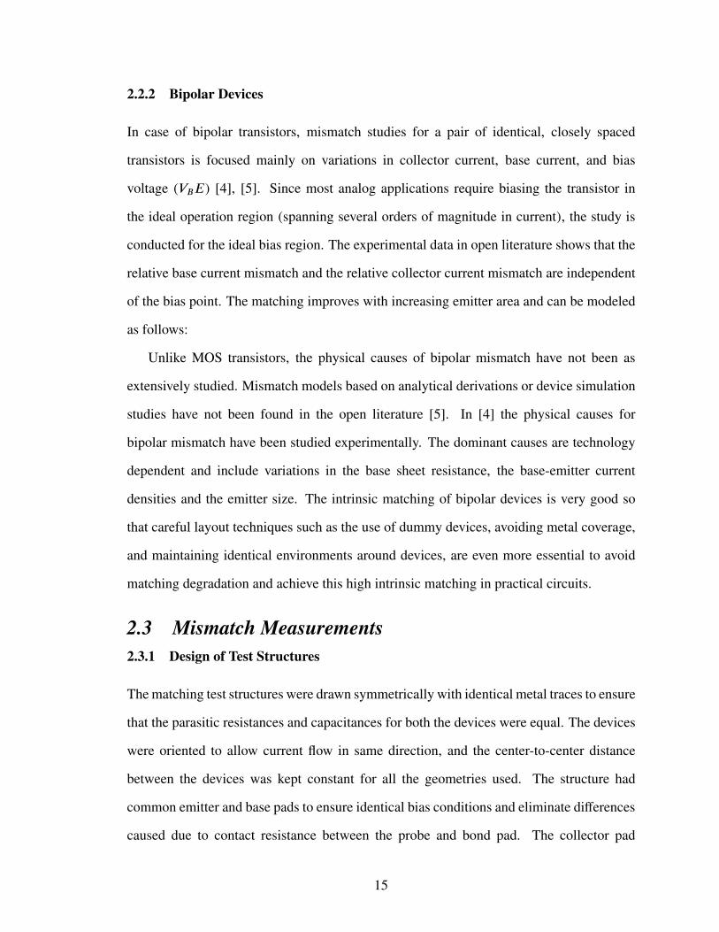
forward-active Gummel characteristics (Figure 8)). As the bias voltage increases, ∆IC /IC
deviates from its constant behavior, due to high current effects and series resistance fluctuations.
As a result, the∆IC /IC values are extracted from the ideal region; a region where mismatch-
sensitive precision analog circuit would likely be biased. Figure 11 shows the statistical
distribution for the 0.4×10.0µm2 device. The histogram follows Gaussian-like distributions,
suggesting that although the sample size is limited (15 devices), it displays the expected
16

Figure 7: (a) Circuit representation of the matching structures;(b) Device geometryavailable.
statistical behavior of classical mismatch, as shown in [7].
In order to quantitatively assess the mismatch fluctuations in these SiGe HBTs, the
standard deviation of the collector current offsets are scaled with respect to emitter area.
Under the conditions given in [7] the standard deviation of the offset is theoretically inversely
proportional to the square root of the active area of the matched component, according to:
σ∆P/P =A∆P/P√WL
(14)
A∆P/P , the so-called "A-factor," is the mismatch fluctuation performance factor used to
facilitate mismatch comparisons between device geometries as well as different technologies.
Referring to Figure 12, the A-factor for the devices is about 4%µm.
17
0.1 0.2 0.3 0.4 0.5 0.6 0.7 0.8 0.9 1.010–12
10–10
10–8
10–6
10–4
10–2
Emitter–Base Voltage (V)
Col
lect
or a
nd B
ase
Cur
rent
Den
sity
(A/µ
m2 )
Forward Mode
AE = 0.4x10.0µm2
VCB = 0V300K
Figure 8: Forward-mode Gummel characteristics.
The observed linear behavior can be attributed to the fact that as device size increases,
the random component of the mismatch decreases. However, the 0.4x1.4µm2 device proves
to be an anomaly to the trend. In this case, current fluctuations can be attributed to gradient
offsets [6]. These offsets become more prevalent as the minimum separation distance
increases. In the case of smaller devices, the minimum separation distance will be higher
in order to maintain the same center-to-center spacing between the test devices.
2.3.3 Summary
In order to comprehend the detrimental effects of mismatch on circuit design, it is essential
to understand the underlying effects that influence device mismatch and isolate the root
causes. This section provided an insight into current mismatch as a function of geometry
in SiGe HBTs. The A-factor can be used to describe mismatch fluctuations for the given
technology to variations in emitter size. This can be particularly useful in analog circuit
18

10–9 10–8 10–7 10–6 10–4 10–3 10–2 10–10
50
100
150
200
250
300
Collector Current Density (A/µm2)
Cur
rent
Gai
n (J
C/J
B)
AE = 0.4x10.0µm2
VCB = 0V300K
Figure 9: Current gain.
blocks that are dependent on the availability of matched pairs. In later sections, the effects
of proton exposure and high temperature on mismatch fluctuations in SiGe HBTs is studied.
19

0.6 0.7 0.8 0.9 1.0
–7–6–5–4–3–2–1
012345
Emitter–Base Voltage (V)
Var
iatio
n in
Col
lect
or C
urre
nt (∆
I c/I c
)(%
)
AE = 0.4x1.4µm2
AE = 0.4x5.0µm2
AE = 0.4x10.0µm2
AE = 0.4x10.0x4µm2
Matching Measurements
Figure 10: Collector current variation as a function of emitter-base bias for a variety ofdevice geometries.
0
1
2
3
4
5
6
7
Variation in Collector Current (∆Ic/Ic)(%)
Num
ber o
f Obs
erva
tions
Pre–radiationAE = 0.4x10.0µm2
300K
Figure 11: Collector current variation histogram.
20

0.0 0.2 0.4 0.6 0.8 1.0 1.2 1.40.0
0.01
0.02
0.03
0.04
0.05
0.06
1/√A (1/µm)
Sta
ndar
d D
evia
tion
(σIc
)
AE = 0.4x1.4µm2
0.4x5.0µm2
0.4x10.0µm2
0.4x10.0x2µm2
0.4x10.0x4µm2
0.4x10.0x8µm2
AE = 0.4x10.0x8µm2
AE = 0.4x1.4µm2
Linear Regression
Figure 12: Standard deviation of the collector current variation as a function of thereciprocal of the square root of the area.
21

CHAPTER III
RADIATION EFFECTS
3.1 Introduction
Today, the challenges associated with electronic systems in space missions forms a major
research area. The study of radiation tolerance is very important since electronic systems
need to operate efficiently under the harsh radiation conditions of the space environment.
Factors such as orbital path, altitude, and duration of flight are involved in determining the
conditions encountered in the mission. Since these conditions vary with every mission,
modeling devices and circuits to perform well in these conditions is a difficult, yet crucial
task. This suggests that device, circuit, and system designers must have a basic understanding
of the radiation environment and its effects on devices and circuits. This chapter provides
an overview of the space radiation environment, basic terminology, and an understanding
of the radiation damage mechanisms.
3.2 Radiation Concepts and Damage Mechanisms
The metric used to quantify the amount of energy an energetic particle or photon deposits
in a particular material is rad (“radiation absorbed dose”) where
1 rad = 100 ergs/gram = 6.24 × 10¹³ eV/gram (15)
The SI unit for total ionizing dose is the grey (Gy) where
100 rad = 1 Grey(Gy) = 1 J/kg (16)
Since the energy absorbed depends on the density of the material, the rad is a material
dependent property. Thus, when using the rad unit, the target material must also be specified.
22

For Si based electronics, typical units are rad(Si) or rad(SiO2), where 1.000 rad(SiO2) =
0.945 rad(Si).
As stated earlier, the space environment contains a mixture of particles detrimental
to devices and circuits. The Earth’s magnetosphere is bombarded by a nearly isotropic
flux of energetic charged particles, primarily the nuclei of atoms stripped of all electrons.
These comprise 85% protons (hydrogen nuclei), 14% a -particles or helium nuclei, and
1% heavier ions covering the full range of elements. Regions of radiation trapped in the
Earth’s magnetic field form belts known as Van Allen belts. Research in this field showed
that these divide into two belts. The inner belt extends to 2.5 Earth radii and the outer belt
extends to about 10 Earth radii. The former comprises of energetic protons up to 600MeV
together with electrons up to several MeV, and the latter comprises of mainly of electrons
and a small quantity of soft protons (0.1 to 5 MeV). The slot region between the belts has
lower intensities but may be greatly enhanced for up to a year following one or two solar
events in each solar cycle. The outer belt is naturally highly time-variable and is driven
by solar wind conditions. An illustration of the interaction between the solar wind and the
Earth’s magnetic is shown in Figure 13.
During solar maximum, the sun contributes to radiation in the space environment.
Events such as solar flares and/or subsequent coronal mass ejections (CME) accelerate
lower energy particles. These solar particle events comprise both protons and heavier ions
and last for several days and tend to vary in composition from event to event. Energies
typically range up to several hundred MeV and have most influence on high inclination or
high altitude systems.
Galactic cosmis rays also contribute to radiation in the space environment. The primary
cosmic rays interact with air nuclei to generate a cascade of secondary particles comprising
protons, neutrons, mesons and nuclear fragments. The intensity of radiation builds up to a
maximum at 18km (Pfotzer maximum) and then slowly drops off to sea level. At normal
aircraft cruising altitudes the radiation is several hundred times the ground level intensity
23

Figure 13: Illustration of the solar wind and radiation belts surrounding the Earth.
24

and at 18km a factor three higher again. Solar particles are less penetrating and only a
few events in each cycle can reach aircraft altitudes or ground level. Some of the neutrons
are emitted by the atmosphere to give a significant albedo neutron flux at low earth orbital
(LEO) spacecraft. It is the decay of these albedo neutrons into protons that is believed to
be the source of the inner radiation belt.
Given the harsh space conditions, electronic systems malfunction due to two major
damage mechanisms : ionization damage and displacement damage. TID ionization and
displacement damage are examined in this section [1], [26], [27], [28].
Total ionizing dose creates electron-hole pairs within dielectric layers (oxides, nitrides
etc.) and subsequent generation of traps at or near the interface with the semiconductor
or of trapped charge in the dielectric. This can produce a variety of device effects such as
flatband and threshold voltage shifts and surface leakage currents. Ionization effects depend
on a number of parameters including the linear energy transfer (LET) of the particle.
The LET is defined as the energy transferred per unit of path traveled by the ionizing
particle normalized by the density of the target material. Both the particle’s LET and the
applied electric field influence the rate of recombination of electron-hole pairs. The dose-
rate influences the relative importance of hole traps and interface states. Since ionization
damage occurs primarily in isolating oxides and in oxide-semiconductor interfaces, the
dose should be defined in relationship to the material affected to avoid errors caused by
considering average doses. Another factor to consider is radiation-induced conductivity,
which is important in mitigating charging of dielectric materials. There are several factors
that need to be considered for total dose effects. TID depends on device bias during
irradiation and annealing effects.
Displacement damage mechanisms also needs to be considered in unhardened devices
to devise a model for space based electronic systems. Energetic particles such as neutrons,
protons, electrons, alpha-particles and heavy ions can create damage in devices by displacing
atoms in the crystal lattice. High-energy protons also lead to production of secondary
25

electrons which can cause displacement effects. The displacement creates stable defect
states within the bandgap giving rise to certain effects depending on the temperature, carrier
concentration and the location at which the defect resides. The presence of defects can lead
to generation of electron-hole pairs, increasing the leakage current in devices. Defects can
also cause ecombination of electron-hole pairs, affecting carrier lifetimes and hence the
dynamic response. Another effect involves trapping of carriers, leading to loss in charge
transfer efficiency in charge-coupled devices in case of minority carrier trapping or carrier
removal in case of majority carrier trapping. Defecs can also lead to compensation of
donors or acceptors by defect centers. Defects can cause increased current in reverse biased
junctions - particularly for small bandgap materials and high electric fields by tunelling of
carriers.
Radiation damage affects the performance of various semiconductor devices in different
ways. This is due to differences in device operation and fabrication. This section reviews
the effects of radiation damage on both Si bipolar transistors and CMOS devices [1],
[26], [27]. However, the inherent robustness to ionizing radiation makes SiGe technology
attractive for many space system applications. Recent studies have reported the proton
tolerance of SiGe HBTs for a variety of different SiGe BiCMOS technologies [1], [31].
This work investigates the proton radiation response of the National BiCMOS8 SiGe HBT
process technology it also investigates, for the first time, the radiation-induced changes in
parametric mismatch fluctuations of SiGe HBTs in identically designed SiGe HBT matched
pairs with different emitter geometries.
3.3 Radiation Effects in SiGe HBTs
The devices used for the study were the standard devices as shown in Table 2. The test
structures were irradiated with 63.3 MeV protons at the Crocker Nuclear Laboratory at the
University of California at Davis. The dosimetry measurements used a five-foil secondary
emission monitor calibrated against a Faraday cup. The radiation source (Ta scattering
26

foils) located several meters upstream of the target establish a beam spatial uniformity of
about 15% over a 2.0 cm radius circular area. Beam currents from about 20 nA to 100 nA
allowed testing with proton fluxes from 1 × 10⁹ to 1 × 10¹² proton/cm2sec. The dosimetry
system has been previously described [29], [30], and is accurate to about 10%. At a proton
fluence 5 × 10¹³ p/cm2, the measured equivalent total ionizing dose was approximately
6,759 krad(Si). The SiGe HBTs were irradiated with all terminals floating, which is
known to present worst case conditions for radiation damage [32]. The structures were
measured at room temperature with an Agilent 4155 Semiconductor Parameter Analyzer.
The radiation exposure and testing conditions were the same for all of the devices measured
to facilitate ambiguous comparisons.
3.3.1 dc Results
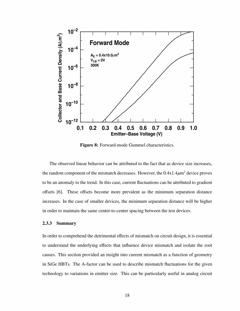
The forward-mode Gummel characteristics for a SiGe HBT subjected to a 63 MeV proton
fluence of 5x10¹³ p/cm2 is shown in Figure 14. Exposure to high proton fluences produces
G/R trapping centers at the emitter-base spacer oxide around the periphery of the transistor
[33]. The increase in base leakage current causes a significant degradation in current gain
(β), as seen in Figure 15.
As a result of irradiation, a slight increase in the collector current is observed between
the matched pairs, as shown in Figure 14. The proton displacement damage in the volume
of the transistor induces a decrease in the net base charge density, which in-turn causes
the neutral base boundary on both the emitter and collector sides of the base to shrink.
This reduces the base Gummel number, increasing the collector current. The National
BiCMOS8 SiGe technology is reasonably tolerant to proton radiation (up to Mrad-level
equivalent dose), without any intentional radiation hardening, as indicated by the above
results.
Similar to the devices measured pre-radiation, the irradiated samples statisticaly follow
a Gaussian-like distribution as shown in Figure 17. Hence, it suggests that although the
27

0.1 0.2 0.3 0.4 0.5 0.6 0.7 0.8 0.9 1.010–12
10–10
10–8
10–6
10–4
10–2
Emitter–Base Voltage (V)
Col
lect
or a
nd B
ase
Cur
rent
Den
sity
(A/µ
m2 )
Forward ModeAE = 0.4x10.0µm2
VCB = 0V300K
Pre–radiation IC, IB5x1013 p/cm2 IC, IB
Figure 14: Forward-mode Gummel characteristics before and after irradiation.
sample size is limited (15 devices), it displays the expected statistical behavior of classical
mismatch, as shown in [7]. Referring to Figure 18, there is negligible difference between
the A-factor for the pre-radiated and post-radiated devices, 4%µm and 4.1%µm respectively.
Comparing the pre-radiated and post-radiated data, there is little observed change in
the standard deviations. Although the collector current slightly increases, the ∆IC /IC
remains approximately the same. This trend can be observed in the magnified version
of the Gummel characteristics shown in Figure 19. To probe this more deeply, Figure 20
shows the correlation between the pre-radiated and post-radiated data. From the graph it
is evident that radiation has little or no effect on collector current mismatch fluctuations,
since the linear regression through the points results in a unity slope (i.e., well correlated).
This lack of radiation-induced change is clearly good news from an analog circuit design
perspective.
28
10–9 10–8 10–7 10–6 10–4 10–3 10–2 10–10
50
100
150
200
250
300
Collector Current Density (A/µm2)
Cur
rent
Gai
n (J
C/J
B)
AE = 0.4x10.0µm2
VCB = 0V300K
Pre–radiation5x1013 p/cm2
Figure 15: Current gain degradation before and after irradiation.
3.3.2 Summary
This chapter provides an insight into the types of radiation encountered in the space environment
and its effects on device and circuit performance via various damage mechanisms. Furthermore,
it provides an understanding of the effects of proton irradiaion in SiGe HBTs and for the
first time, the effects of proton exposure on mismatch fluctuations in SiGe HBTs. The
change in collector current (Ic) variation is negligible after 5x10¹³ p/cm2 proton fluence,
indicating that collector current mismatch should not be a major issue for space-borne
analog circuits utilizing SiGe HBTs.
29

0.6 0.7 0.8 0.9 1.0
–7–6–5–4–3–2–1
012345
Emitter–Base Voltage (V)
Var
iatio
n in
Col
lect
or C
urre
nt (∆
I c/I c
)(%
)
AE = 0.4x1.4µm2
AE = 0.4x5.0µm2
AE = 0.4x10.0µm2
AE = 0.4x10.0x4µm2
Matching Measurements
Pre–radiation5x1013 p/cm2
Figure 16: Collector current variation as a function of emitter-base bias for a variety ofdevice geometries.
0
1
2
3
4
5
6
7
–8 0 8
Num
ber o
f Obs
erva
tions
Variation in Collector Current (∆Ic/Ic)(%)
5x10¹³ p/cm2
AE = 0.4x10.0µm2
300K
Figure 17: Collector current variation histogram - post-radiation.
30

0.0 0.2 0.4 0.6 0.8 1.0 1.2 1.40.0
0.01
0.02
0.03
0.04
0.05
0.06
1/√A (1/µm)
Sta
ndar
d D
evia
tion
(σIc
)
AE = 0.4x1.4µm2
0.4x5.0µm2
0.4x10.0µm2
0.4x10.0x2µm2
0.4x10.0x4µm2
0.4x10.0x8µm2
AE = 0.4x10.0x8µm2AE = 0.4x1.4µm2
Linear Regression
Pre–radiation5x1013 p/cm2
Figure 18: Standard deviation of the collector current variation as a function of thereciprocal of the square root of the area.
31

0.615 0.616 0.617 0.618 0.619 0.621.75x10–7
2.00x10⁻⁷
2.25x10⁻⁷
2.50x10⁻⁷
2.75x10⁻⁷
Emitter–Base Voltage (V)
Col
lect
or a
nd B
ase
Cur
rent
Den
sity
(A/µ
m2 )
Forward ModeAE = 0.4x10.0µm2
VCB = 0V300K
Pre–radiation
5x10¹³ p/cm2
JC1
JC2JC1
JC2
Figure 19: Collector currents for each transistor of the matched pair for both pre-radiationand post-radiation.
32

–5 –4 –3 –2 –1 0 1 2 3 4 5–5
–4
–3
–2
–1
0
1
2
3
4
5
Pre–radiation Variation (%)
Pos
t–ra
diat
ion
Var
iatio
n (%
)
Variation in Collector Current (∆Ic/Ic)(%)
AE = 0.4x10.0µm2
5x10¹³ p/cm2
Unity Slope
Figure 20: Correlation of collector current variation between pre-radiation and post-radiation.
33
CHAPTER IV
TEMPERATURE MISMATCH EFFECTS
4.1 Introduction
Given the expanding realm of electronic systems applications, research conducted in high-
temperature electronics has gained popularity with applications such as automobiles, heavy
vehicles, power switching, engine electronics, aerospace (e.g., the oall electric aircrafto),
shipping, oil well logging, nuclear power, planetary space missions, and radar systems [41].
Several technologies have been used in these applications including SOI CMOS, GaAs,
and SiC. Traditional Si CMOS and bipolar transistor operations are typically limited to
temperatures below 200 C due to junction leakage currents [45] and reliability concerns.
These issues occur since these transistors use reverse-biased p-n junctions for electrical
isolation. However, these device technologies require extensive (costly) modification in
order to provide consistent performance at high-temperatures.
SiGe HBT BiCMOS technology has recently attracted interest because of its inherent
advantages over Si bipolar transistors and its growing applications in analog, RF, digital,
and microwave applications. As stated earlier, SiGe HBTs utilizes efficient bandgap engineering
that favors cryogenic operations while causing degradation in device performance at higher
temperatures. However, [39] and [40] demonstrates that, contrary to popular opinion, SiGe
HBTs are potentially well-suited for many high temperature electronics applications.
4.2 High Temperature Concepts
There are several challenges associated with high-temperature electronic applications with
transistor reliability being most crucial [42], [43]. A major concern in p-n junction devices
is the increase in junction leakage current with increasing temperature. This effect can be
34

attributed to the thermal generation of carriers in the junctions.
Thermal generation of carriers depends exponentially on temperature and bandgap
(kT/Eg). As shown in Figure 21a, thermal excitation provides electrons with enough
energy to move from the valence band to the conduction band (direct thermal generation).
However, thermally assisted generation of carriers with R-G centers acting as intermediaries
can be seen in Figure 21b. As a result, as temperature increases, the leakage current
increases. In case of devices with larger bandgaps, the probability of an electron moving
from the top of the valence band into the conduction band is lower. As a result, the electrons
require higher energy to jump across the gap, lowering the leakage current. However,
since the bandgap is also dependent on temperature, the band gap energy decreases as the
temperature increases. Thus, at elevated temperature, leakage current increases. Another
factor that affects thermal generation depends on whether the semiconductor has a direct or
indirect bandgap. Consequently, generation of carriers in the junctions will be more rapid
for direct than for indirect bandgap semiconductors for a given bandgap. Zipperian [42]
sets a maximum acceptable leakage current (0.1 A/cm2), and hence provides a range of
operation for the various technologies at high-temperature.
Another physical effect that impacts high-temperature performance in p-n junction
transistors is an increase in the intrinsic carrier density with temperature. For an intrinsic
semiconductor, we can write,
ni = 2πkT/h23/2mhme
3/4e−Eg/2kT (17)
where Eg0 is the energy gap, EC u EV , k is the Boltzmann’s constant, h is the Planck’s
constant, and me and mh are the electron and hole effective masses respectively. The
strong dependence of the carrier concentration on bandgap and temperature is evident
from Equation ??. The smaller the bandgap, the greater the probability of an electron
moving from the top of the valence band into the conduction band, since less energy is
required for the electron. Similarly, the higher the temperature of a device, the greater
35

Figure 21: Energy band visualization of thermal generation processes.
36

the energy imparted to the electrons in the valence band, and hence larger the number of
electrons that have the sufficient energy to jump across the gap. Thus electron and hole
densities increase with temperature and decrease with increasing Eg. As the temperature
increases, the increased thermal energy ionizes significant numbers of the semiconductor
atoms themselves (for example the Si atoms) in addition to the dopant atoms. This contributes
additional electrons and holes in the conduction and valence and bands and, more important,
results in approximately equal numbers of carriers in each band, independent of the doping,
resulting in a condition called intrinsic. Since there are orders of magnitude more semiconductor
atoms than dopant atoms, the influence of the dopant is overwhelmed at a sufficiently high
temperature and hence, the junctions are owashed outo.
In most situations, circuits designed to operate at high-temperature are also required to
perform efficiently over a wide range of temperatures. Several device parameters such as
Fermi level, intrinsic carrier density, carrier generation rate, and carrier mobility depend
on temperature [46]. This causes certain device characteristics to vary with temperature,
causing variance in conductances, transconductances, leakage currents, diode voltage drops,
and FET threshold voltages. Reliability also forms a central issue for high-temperature
circuit operation because high temperature accelerates many device and circuit wearout
mechanisms. As a result, in order to attain required circuit performance over a wide
temperature range, designers need to understand the physical and electrical behavior for
the entire temperature range.
Device mismatch has been a deterrent to obtaining optimum circuit performance in
precision analog circuits at room temperature. Certain applications such as oil drilling
require ADC to operate efficiently at high temperatures. As such, device mismatch effects
at high-temperature have not been seriously studied. This is probably because the temperature
effects are believed to be insignificant to transistor mismatch. Hence, none of the mismatch
models existing today include temperature effects. However, results presented in [44] for
MOS mismatch, suggest a noticeable improvement in drain current and threshold voltage
37

0.1 0.2 0.3 0.4 0.5 0.6 0.7 0.8 0.9 1.010–12
10–10
10–8
10–6
10–4
10–2
Emitter–Base Voltage (V)
Col
lect
or a
nd B
ase
Cur
rent
Den
sity
(A/µ
m2 )
Forward ModeAE = 0.4x10.0µm2
VCB = 0V300K
IC
IB
25°C50°C75°C100°C
Figure 22: Forward-mode Gummel characteristics as a function of temperature.
mismatch as temperature increases. This work investigates the effect of high-temperature
on transistor mismatch in SiGe HBTs, for the first time, in order to demonstrate their
applicability in high-temperature precision analog circuits.
4.3 Temperature Effects4.3.1 Results
The devices used for the study were the standard devices as shown in Table 2. SiGe HBTs
were measured on-wafer using Agilent 4155 C on probe stations capable of operating 20 C
to 100 C.
Figure 22 shows the the Gummel characteristics of the SiGe HBTs at 25 C, 50 C, 75
C, and 100 C. The decrease in turn-on voltage is evident from Figure 22 with increasing
temperature. This effect is due to the change in the intrinsic carrier concentrations, hence,
causing a decrease in the emitterubase built-in potential.
38
10–9 10–8 10–7 10–6 10–4 10–3 10–2 10–10
50
100
150
200
250
Collector Current Density (A/µm2)
Cur
rent
Gai
n (J
C/J
B)
AE = 0.4x10.0µm2
VCB = 0V300K
25°C50°C75°C100°C
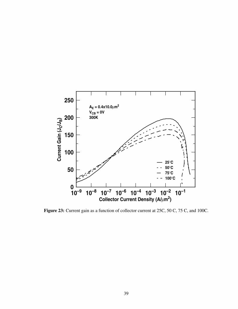
Figure 23: Current gain as a function of collector current at 25C, 50 C, 75 C, and 100C.
39

0 10 20 30 40 50 60 70 80 90 100 1100.01
0.0125
0.015
0.0175
0.02
Temperature (°C)
Sta
ndar
d D
evia
tion
(σIc
)
AE = 0.4x10.0µm2
Figure 24: Standard deviation of the collector current variation as a function oftemperature.
The current gain of the measured SiGe HBTs at 25 C, 50 C, 75 C, and 100 C are
shown in Figure 23. As expected, the peak current gain decreases as temperature increases.
Equation 4 shows the influence of temperature on β of the device. The device maintains
ideality upto 100 C with current gain greater than 100. Its hould also be noted that the
device has higher current drive capability at temperatures higher than room temperature.
This suggests that the impact of high temperatures on the carrier mobility and hence series
resistances is not detrimental to circuit performance. However, parasitic leakage caused by
minority carrier generation in the collector-substrate junction could limit high temperature
applications [40].
Figure 24 illustrates how the variation in collector current changes with repect to temperature.
As temperature increases, the standrad deviation of the current variation decreases. Hence,
at higher temperatures, collector current mismatch improves. This suggests that devices
and circuits will operate closer to simulated values from the matching standpoint at the
40

higher temperatures. This allows designers room for experimentation in design space since
it relaxes the trade-offs circuit designers need to make in order to obtain optimum circuit
performance in precision analog circuits.
4.3.2 Summary
This chapter accessed the applicability of using SiGe HBTs for high-temperature analog
design applications. It was observed that the Sige HBTs not only exhibit sufficient gain
but also see reduced collector current variation at high temperatures. These features would
promote the use of SiGe HBTs for high temperature applications.
41
CHAPTER V
CONCLUSION
5.1 Conclusion
The purpose of this work was to investigate the effects of device mismatch in SiGe HBT
BiCMOS technology under extreme conditions such as radiation and high temperatures.
Matched pairs are critical in many types of analog circuits, including differential pairs
for the input stages of amplifiers, current mirrors for biasing, and in various circuits topologies
utilizing integer multiples of identical components such as bandgap references, ADCs,
DACs, and filters. Thus, accurate transistor matching is at the very heart of robust analog
circuit design. Chapter II explores the fundamentals of device mismatch and explores for
the first time the collector current variations in SiGe HBTs. Our study indicates geometric
dependence on collector current variation, as expected, the excpetion being the smallest
device geometry. The computed A-factor is comparable if not better than other device
technologies.
Chapter III examined the effects of radiation on various SiGe HBT BiCMOS technologies.
The space community is increasingly using COTS parts in spaceborne systems, thus radiation
testing on new commercial technologies is imperative. The effects of proton irradiation on
matched device pairs on a new commercially-available SiGe technology were examined for
the first time. We report that proton induces some damage in the SiGe HBT operating in
forward-mode. However, our findings indicate that the dc circuit performance is total dose
tolerant up to Mrad-level equivalent total dose.
Chapter IV presents the results of the effects of collector current mismatch at high
temperatures. As such, device mismatch effects at high-temperature have not been seriously
studied. This is probably because the temperature effects are believed to be insignificant to
42

transistor mismatch. However, our results suggest a noticeable improvement in collector
current mismatch as temperature increases. This characteristic is essential in order to prove
its applicability in high-temperature precision analog circuits.
5.2 Future Directions
The focus of this work was in obtaining in-depth understanding of collector current mismatch
under different conditions. Further investigation could involve examining base current
and emitter-base voltage variations under similar conditions in order to prvide a complete
picture of device mismatch in SiGe HBTs. Furthermore, these measurements could be
applied to a generation of technologies in order to understand the change in device mismatch
with technology scaling. The results obtained in this study could also be used to generate
models that account for device mismatch in order to facilitate circuit designers by providing
worst condition simulations capabilities. This will allow circuit designers to account for
variability in their designs.
43

REFERENCES
[1] J.D. Cressler and G. Niu, Silicon-Germanium Heterojunction Bipolar Transistors,Artech House, Boston, 2003.
[2] Kaicheng Li, Daoguang Liu, Wei-Xin Ni, Yue Hao, Jing Zhang, Zhengfan Zhang,Shiliu Xu, Gangyi Hu, and Lin Guo, “Growth and quality control of MBE SiGe-HBTstructures for analog IC applications, ” Solid-State and Integrated-Circuit Technology,vol. 1,a pp. 586 u 591, 2001.
[3] D.L. Harame, J.M.C. Stork, B.S. Meyerson, K.Y.-J. Hsu, J. Cotte, K.A. Jenkins,J.D. Cressler, P. Restle, E.F. Crabbe, S. Subbanna T.E. Tice, B.W. Scharf, and J.A.Yasaitis, “Optimization of SiGe HBT technology for high speed analog and mixed-signal applications, ”Technical Digest IEEE International Electron Devices Meeting,pp. 71-74, 1993.
[4] P.G. Drennan, C.C. McAndrews, J. Bates, and D, Schroder, “ Rapid evolution of theroot causes on BJT mismatch,” Proceedings of the International Microelectronic TestStructure, pp. 122-127, 2000.
[5] H.P. Tuinhout, “ Design of matching test structures,” Proceedings of the InternationalMicroelectronic Test Structure, pp. 21-27, 1994.
[6] P.G. Drennan, “ Device Mismatch in BiCMOS Technologies,” Proceedings of theBipolar/BiCMOS Circuits and Technology Meeting, pp. 104-111, 2002.
[7] H.P. Tuinhout, “ Improving BiCMOS technologies using BJT parametric mismatchcharacterisation,” Proceedings of the Bipolar/BiCMOS Circuits and TechnologyMeeting, pp. 163-170, 2003.
[8] H. Kromer, “ Two integral relations pertaining to electron transport through a bipolartransistor with a nonuniform energy gap in the base region,” Solid-State Electronics,vol. 28, pp. 1101–1103, 1985.
[9] M. Pelgrom, H. Tuinhout, and M. Vertregt, “Transistor matching in analog CMOSapplications,” Technical Digest IEEE International Electron Device Meeting pp.915u918, 1998.
[10] J. Shyu, G. C. Temes, and F. Krummenacher, “Random error effects in matched MOScapacitors and current sources,” IEEE J. Solid-State Circuits, vol. SC-19, no. 6, pp.948u955, 1984.
[11] K. R. Lakshmikumar, R. A. Hadaway, and M. A. Copeland, “Characterization andmodeling of mismatch in MOS transistors for precision analog design,” IEEE J. Solid-State Circuits, vol. 21, no. 6, pp. 1057u1066, 1986.
44

[12] M. Pelgrom, A. Duinmaijer, and A. Welbers, “Matching properties of MOStransistors,” IEEE J. Solid-State Circuits, vol. 24, no. 5, pp. 1433u1439, 1989.
[13] J. Bastos, M. Steyaert, R. Roovers, P. Kinget, W. Sansen, B. Graindourze, N.Pergoot, and E. Janssens, “Mismatch characterization of small size MOS transistors,”Proceedings of the International Microelectronic Test Structure, pp. 271u276, 1995.
[14] J. Horstmann, U. Hilleringmann, and K. Goser, “Matching analysis of depositiondefined 50-nm MOSFETÆs,” IEEE Transactions on Electron Device, vol. 45, no. 1,pp. 299u306, 1998.
[15] T.-H. Yeh, J. Lin, S.-C. Wong, H. Huang, and J. Sun, “Mis-match characterization of1.8 V and 3.3 V devices in 0.18 µ m mixed signal CMOS technology,” Proceedings ofthe International Microelectronic Test Structure, pp. 77u82, 2001.
[16] Y. Tsividis, Operation and Modeling of the MOS Transistor, 2nd ed. Oxford, U.K.:Oxford Univ. Press, 2003.
[17] L. Portmann, C. Lallement, and F. Krummenacher, “A high density integrated testmatrix of MOS transistors for matching study,” Proceedings of the InternationalMicroelectronic Test Structure, pp. 19u24, 1998.
[18] P. Drennan and C. McAndrew, “Understanding MOSFET mismatch for analogdesign,” IEEE J. Solid-State Circuits, vol. 38, no. 3, pp. 450u456, 2003.
[19] J. Croon, M. Rosmeulen, S. Decoutere, W. Sansen, and H. Maes, “An easy-to-usemismatch model for the MOS transistor,” IEEE J. Solid- State Circuits, vol. 37, no. 8,pp. 1056u1064, 2002.
[20] F. Forti and M. Wright, “Measurement of MOS current mismatch in the weakinversion region,” IEEE J. Solid- State Circuits, vol. 29, no. 2, pp. 138u142, 1994.
[21] J. Bastos, M. Steyaert, B. Graindourze, and W. Sansen, “Matching of MOS transistorswith different layout styles,” Proceedings of the International Microelectronic TestStructure, pp. 17u18, 1996.
[22] H. Tuinhout, M. Pelgrom, R. P. de Vries, and M. Vertregt, “Effects of metalcoverage on MOSFET matching,” Technical Digest IEEE International ElectronDevice Meeting, pp. 735u738, 1996.
[23] E.J. Prinz, P.M. Garone, P.V. Schwartz, X. Xiao, and J.C. Sturm, “Theeffect of emitter-base spacers and strain-dependent density-of-states in Si/SiGe/Siheterojunction bipolar transistors,” Technical Digest IEEE International ElectronDevice Meeting, pp. 639–642, 1989.
[24] D.L. Harame, J.H. Comfort, J.D. Cressler, E.F. Crabbe, J.Y-C. Sun, B.S. Meyerson,and T. Tice, “Si/SiGe epitaxial-base transistors – part I: materials, physics, andcircuits,” IEEE Transactions on Electron Device, vol. 42, pp. 455–468, 1995.
45

[25] S.S. Iyer, G.L. Patton, J.M.C. Stork, B.S. Meyerson, and D.L. Harame,“Heterojunction bipolar transistors using Si-Ge alloys,” IEEE Transactions onElectron Device, vol. 36, pp. 2043–2064, 1989.
[26] J.R. Srour and J.M. McGarrity, “Radiation Effects on Microelectronics in Space,”Proceedings of the IEEE, vol. 76, pp. 1443-1469, 1988.
[27] C. Claeys and E. Simoen, Radiation Effects in Advanced Semiconductor Materialsand Devices, Springer, Berlin, 2002.
[28] J.R. Srour, C.J. Marshall, and P.W. Marshall, “Review of displacement damage effectsin silicon devices,” IEEE Transactions on Nuclear Science, vol. 50, pp. 653-670, 2003.
[29] K.M. Murray, W.J. Stapor, and C. Casteneda, “Calibrated charged particle radiationsystem with precision dosimetric measurement and control,"” Nuclear Instrumentsand Methods in Physics Research, vol. A281, pp. 616-621, Sept. 1989.
[30] P.W. Marshall, C.J. Dale, M. A. Carts, and K.A. LaBel, "Particle-induced bit errorsin high performance fiber optic data links for satellite data management", IEEETransactions on Nuclear Science, vol. 41, No. 41, pp. 1958-1965, December 1994.
[31] J.P. Comeau, A.K. Sutton, B.M. Haugerud, J.D. Cresser, W-M.L. Kuo, P.W. Marshall,R.A. Reed, A. Karroy, and R. Van Art, “Proton tolerance of advanced SiGe HBTsfabricated on different substrate materials,” IEEE Transactions on Nuclear Science,vol. 51, pp. 3743-3247, 2004.
[32] S. Zhang, J.D. Cressler, G. Niu, C.J. Marshall, P.W. Marshall, H.S. Kim, R.A. Reed,M.J. Palmer, A.J. Joseph, and D.L. Harame, “The effects of operating bias conditionson the proton tolerance of SiGe HBTs,” Solid-State Electronics, vol. 47, pp. 1729-1734, 2003.
[33] J.D. Cressler, R. Krithivasan, G. Zhang, G. Niu, P.W. Marshall, H.S. Kim, R.A.Reed, M.J. Palmer, and A.J. Joseph, “An investigation of the origins of the variableproton tolerance in multiple SiGe HBT BiCMOS technology generations,” IEEETransactions on Nuclear Science, vol. 49, pp. 3203-3207, 2002.
[34] S. R. Stiffler et al., “The Thermal Stability of SiGe Films Deposited by Ultrahigh-Vacuum Chemical Vapor Deposition,” Journal of Applied Physics, vol. 70, no. 11, pp.7194, 1991.
[35] G. L. Patton et al., "SiGe-Base Heterojunction Bipolar Transistor by Molecular BeamEpitaxy," IEEE Electron Device Letters, vol.9, no. 4. pp. 165-167, 1988.
[36] J. F. Gibbons et al., "Limited Reaction Processing: Silicon Epitaxy," Applied PhysicsLetters, Vol. 47, pp. 165-167, 1988.
[37] T. O. Sedgwick et al., " High Phosphorus Doping of Epitaxial Silicon at LowTemperature and Atmospheric Pressure," Applied Physics Letters, vol. 58, no. 14,pp. 1896-1898, 1991.
46
[38] B. S. Meyerson et al., "Low-Temperature Silicon Epitaxy by Ultrahigh VacuumChemical Vapor Deposition," Applied Physics Letters, vol. 48, no. 12, pp. 797-799,1986.
[39] T. Chen, W. M. L. Kuo, E. Zhao, Q. Liang, Z. Jin, J. D. Cressler, and A. J. Joseph,“On the suitability of SiGe HBTs for high-temperature (to 300 C) electronics,”Proceedings of the Bipolar/BiCMOS Circuits and Technology Meeting, pp. 217u220,2004.
[40] T. Chen, W. M. L. Kuo, E. Zhao, Q. Liang, Z. Jin, J. D. Cressler, and A. J. Joseph,“On the high-temperature (to 300/spl deg/C) characteristics of SiGe HBTs,” IEEETransactions on Electron Devices, Vol. 51, pp. 1825-1832, 2004.
[41] P. L. Dreike, D. M. Fleetwood, D. B. King, D. C. Sprauer, and T. E. Zipperian,“An overview of high-temperature electronic device technologies and potentialapplications,” IEEE Trans. Comp., Packag., Manufact. Technol. A, vol. 17, pp.594u609, 1994.
[42] T. E. Zipperian, “A survey of inaterials and device technologies for high temperature(T > 3OOC) power semiconductor electronics,” Proceedings of the Power ConversionIntelligence, pp. 353-365, 1986.
[43] S . Pzyqbylko, “High temperature electronics for aircraft engines,” Proceedings of theAIAA/SAMASME/ASEE 261h Joint Propulsion Conference, pp. 1-6, 1990.
[44] P. B. Y. Tan and A. V. Kordesch, “Thermal effect on matching of MOS transistorthreshold voltage and drain current,” IEEE National Symposium on Microelectronics,pp. 35-38, 2003.
[45] D. W. Palmer and R. C. Heckman, “Extreme temperature range electronics,” IEEETrans. Comp., Hybrids Munuf. Technology, vol. CHMT-I , pp. 333-340, 1978.
[46] R. F. Pierret, Semiconductor Device Fundamentals, Addison-Wesley PublishingCompany, Inc., 1996.
47