Safety laminated glass interlayer eva interlayer fim, pvb interlayer film, sgp interlayer film
Upload
truongnguyetCategory
view
216download
0
Characterization of Low k CVD Deposited Interlayer Dielectricsfor Integrated Circuits
by
Marnie L. Harker
S.B Materials Science and EngineeringMassachusetts Institute of Technology (February, 1996)
SUBMITTED TO THE DEPARTMENT OF MATERIALSSCIENCE AND ENGINEERING IN PARTIAL
FULFILLMENT OF THE REQUIREMENTS FOR THE DEGREE OF
MASTER OF SCIENCE IN MATERIALS SCIENCE AND ENGINEERINGAT THE
MASSACHUSETTS INSTITUTE OF TECHNOLOGY
SEPTEMBER 1997
© 1997 Marnie L. Harker. All rights reserved.
The author hereby grants to MIT permission to reproduceand to distribute publicly paper and electronic
copies of this thesis document in whole or in part.
Signature of Author:Department of Materials Science and Engineering
August 8, 1997
Certified by:Professor Karen K. Gleason
Associate Professor of Chemical EngineeringThesis Supervisor
Read by:Professor Klavs Jensen
rofessor of Chemical Engineering / Materials Science and EngineeringThesis Reader
Accepted by:Professor Linn Hobbs
John F. Elliott Professor of MaterialsChair, Departmental Committee on Graduate Students
DEC 2 4197LlIAfNES

Characterization of Low k CVD Deposited Interlayer Dielectricsfor Integrated Circuits
by
Marnie L. Harker
Submitted to the Department of Materials Scienceand Engineering on August 8, 1997 in Partial Fulfillmentof the Requirements for the Degree of Master of Science
in Materials Science and Engineering
ABSTRACT
Decreasing the device dimensions in integrated circuits improves device performance andyield but leads to interconnect issues such as increased crosstalk, RC delay, and line-to-line powerdissipation. New interlayer dielectric materials are required to meet the needs of the sub-quartermicron microprocessor generations.
Two CVD deposited low dielectric constant Interlayer Dielectric materials, parylene-F andamorphous fluorocarbon were characterized with respect to the primary criteria of thermalstability up to 450'C, adhesion comparable to that of the current ILD, SiO2, and dielectricconstant less than 2.5. Both materials were shown to have low dielectric constants: 2.25 forParylene-F and -2.4 for the amorphous fluorocarbons, but additional work is required to meet theother criteria.
After a 400'C anneal, parylene-F was found to be thermally stable up to 4250 C, but itsadhesion strength was low even with the use of adhesion promoters. The amorphous fluorinatedcarbons showed moderate adhesion strength, although still lower than SiO2, but they were notthermally stable even after annealed for 2 hours at 4000 C. Water, either incorporated in the filmor sorbed onto the surface may have provided the oxygen to cause continuous CO and CO 2evolution from the film. NMR and XPS suggest that the fluorocarbon films may have afluorinated graphite (C2F)n structure. Although the dielectric films are amorphous, obtaining amore C2F -like structure could offer a direction for improvement of amorphous fluorocarbon toachieve the high thermal stability (up to 590C in vacuum) and possible low polarizability offluorinated graphite. Further development is required on both of these materials if they are to beused in integrated circuits.
Thesis Supervisor: Karen GleasonTitle: Associate Professor of Chemical Engineering
Thesis Supervisor: Klavs JensenTitle: Professor of Chemical Engineering / Materials Science and Engineering

ACKNOWLEDGEMENTS
I would like to take this opportunity to acknowledge all the people who have assisted,guided and prodded me in the completion of my Master's thesis. Without you all, my sleeplessnights might all have been in vain.
First I want to express my sincere thanks to my MIT advisors, Professor Karen Gleasonand Professor Klaus Jensen. Professor Gleason provided me not only with invaluable technicalguidance, but also with lab time and equipment and even the loan of a couple of her own gradstudents. I appreciate the time they have both spent in reading and reviewing my thesis as well astheir insight into this project.
I would also like to express my gratitude to my supervisors at Intel Corporation, Dr.Indrajit Banerjee, and Dr. David Fraser. They made this project possible, and offered me not onlythesis guidance but also career guidance for which I would like to thank them both. In addition, Iwould like to thank Larry Wong and Steven Towle for reviewing my thesis and for helping mealong these last eight months.
Without the help of several people, much of this data would never have been collected. Iwould like to thank Rey Villasol, Tae Han, and Chuabin Pan for training me on the many pieces ofequipment in the lab and for never failing to answer my ceaseless questions. Thanks to those whoran experiments for me including Peter Coon, Leslie Serrano, and Armando Cobarrubia. Inaddition, I would like to recognize Ken Lau and Ming Liao for all of the time they devoted to meto help me through my two weeks of NMR.
Finally, I would like to thank my friends and family, because without them, I would neverhave gotten to where I am. To my Dad who understood why I love engineering, to my Mom whohas never failed to support me in any decision, and to Amy and Chris who have always been therefor me, I'd like to give a loving thank you. To the friends who are still my friends despite myabsence these past months in the pursuit of science, I would like to say, thanks for being there,and let's go to the beach!

For Dad, if only you could have been here for this...

TABLE OF CONTENTS
1 Introduction ....................................................................................................... 82 B ackgroun d ............................................................................................................ 12
2.1 M otivation.......................................................................................................... 122.2 Materials Selection.........................................................16
2.2.1 Selection Criteria......................................................................... 162.2.2 Ultra Low k Materials.............................................. 20
2.2.2a Parylene-F.................................................................... 202.2.2b Fluorinated Amorphous Carbon (a-C:F)........................... 22
2.3 G raphite Fluoride......................................... ................................................ 223 Experimental Procedures and Methods............................... ............. 26
3.1 Sample Description..................................................... 263.2 Compositional and Structural Analysis................................ ............. 273.3 Therm al Stability......................................... ................................................ 28
3.3.1 Thermogravimetric Analysis (TGA)................................ ....... 283.3.2 Thermal Desorption Spectroscopy (TDS)................................... 29
3.4 A dhesion............................................................................................................ 3 13.5 Electrical Characterization............................................. 31
4 Results and Discussion................................................... 333.1 Compositional and Structural Analysis................................ ............. 333.2 Therm al Stability......................................... ................................................ 46
3.3.1 Thermogravimetric Analysis (TGA)................................ ....... 463.3.2 Thermal Desoprtion Spectroscopy (TDS)............................ ....... 47
3.4 A dhesion............................................................................................................ 553.5 Electrical Characterization............................................. 58
5 C onclusions............................................................................................................ 60B ibliography ............................................................................................................ 62

LIST OF FIGURES
2-1 Schematic of shrinking device dimensions in metal/ILD system............................ 132-2 Two graphs of wiring capacitance dominating gate delay................................. 152-3 Polarizability of a material as a function of frequency................................. 182-4 Chemical structure of parylene variants.......................................................... 212-5 Structure of (C 2F) ......................................................................................... ........ 232-6 Cls XPS data from two type of C F ................................... 243-1 TGA test apparatus............................... ............................. 283-2 TGA temperature profile..................................................... 293-3 TD S test apparatus................................................................................................ 304-1 FTIR spectra for parylene-F................................................. 334-2 FTIR spectra for pulsed plasma PECVD PTFE................................................ 354-3 FTIR spectra of amorphous fluorocarbon ...................................... .......... 364-4 Cls XPS results for HDP-2 amorphous fluorinated carbon............................... 384-5 Cls XPS of modified HDP-2* film................................................................. 394-6 Bond type concentrations calculated from XPS................................. ........ 404-7 NM R spectra for parylene-F............................................................................. 424-8 NM R spectra for PECVD .............................................................................. 434-9 NMR spectra for HDP-2...................................................... 444-10 NMR data broken down into percentages of C-F bond types.............................. 454-11 TGA graph for parylene-F............................................................................... 474-12 TDS results for parylene-F................................................. 484-13 TDS data for amorphous fluorocarbons.......................... 504-14 TDS results for HDP-2 fluorocarbon............................................................... 514-15 TDS data for HDP-2 with 50oC/min ramp rate................................................ 524-16 Slopes from Arrhenius plot of thermal decomposition.................................... 544-17 TDS results of second heat cycle for HDP-2.................................. .......... 554-18 Low magnification SEMs of parylene-F......................... 574-19 Higher magnification SEMs of parylene-F........................... ... .............. 584-20 Frequency dependence of capacitance............................................................ 59

LIST OF TABLES
1-1 SIA R oadm ap ....................................................................................................... 92-1 Estimated interconnect RC delay to transistor RC delay.................................. 162-2 Table of materials requirements for low k ILD................................................ 173-1 Types of wafer substrates and their uses.................................. ............ 263-2 Experiment Matrix............................................................. 274-1 XPS and AES composition results............................................... 414-2 Summary of TGA results..................................................... 464-3 Identifications of commonly detected ion masses from TDS............................... 534-4 A dhesion strength............................................. .............................................. 554-5 D ielectric constant........................................... ............................................... 59

CHAPTER 1. INTRODUCTION
The drive to decrease chip dimensions and increase device density presents the
opportunity to incorporate new materials like low dielectric constant organics into integrated
circuits. Because the industry standard dielectric, SiO 2 is no longer sufficient due to its high
dielectric constant, research into the previously solved problem of dielectrics for integrated
circuits has been revitalized. This paper will discuss the characterization of two low k organic
materials, parylene-F and amorphous fluorocarbon, which have the potential to meet the low k
needs of future microprocessor generations.
As the number of metal layers increases and line widths drop to and below 0.18 pm, RC
delay reduction is necessary to increase clock speed and reduce crosstalk. Resistance and
capacitance must also be lowered to minimize power consumption through resistive heating and
dielectric loss. Because of its lower resistance, copper is being investigated as an alternative to
aluminum interconnects.1, 2 Assuming that the risk of diffusion into copper sensitive devices
could be eliminated, substituting copper in place of aluminum would not counteract the effect of
denser interconnects once feature size drops below 0.25 p.m unless the capacitance is reduced as
well.3
Many materials have a dielectric constant lower than that of SiO2 (k>4), however, other
criteria such as thermal stability, good adhesion, gapfill, and conformality, manufacturability,
reliability, and environmental risk as well as cost, throughput time, and yield must be met for a
new material to be introduced into a chip. It must be thermally stable throughout all subsequent
processing steps. Back end of the line processing steps, including metals deposition occur a
temperatures around 450'C,5 so this temperature is set for the lower boundary thermal stability

requirement. It must have sufficient adhesion to many different materials in an integrated circuit,
including silicon, SiO 2, metals, and diffusion barrier layers, both on the surface and on the
sidewalls of trenches. Because dielectrics isolate aluminum lines they must also fill gaps and
conform well to topography, although if the industry switches to a Damascene process rather
than metal deposition/trench etch, this trait would no longer be necessary.
These factors indicate that the best choice for a low k dielectric might be one that is most
like silicon dioxide, to introduce as little variation to the process as possible. Substituting
oxygen atoms with fluorine potentially lowers the dielectric constant of fluorinated SiO2 to as
low as 3.2, using the same type of Chemical Vapor Deposition (CVD) reactor as standard SiO2.
The addition of fluorine, however, reduces the stability and adhesion of the film, and introduces
the threat of fluorine or HF outgassing, which is both a silicon dioxide etchant and a health
threat. The resolution of these issues to obtain a useful film, however, will still not meet the low
k needs of the 0.18 jtm generation or subsequent scalings.6 Table 1-1 shows that the
Semiconductor Industry Association (SIA) predicts that a dielectric constant below 2.4 is
necessary for generations beyond 0.25 pm, a more exotic solution that SiOF is required.
Table 1-1: SIA roadmap '
Year k Critical Dimension # of Metal(gate length) Levels
1995 3.8 0.35 4-5
1998 3.0 0.25 5
2001 2.0-2.4 0.18 5-6
2004 <2.0 0.13 6

Two promising materials with dielectric constants at or below 2.4 are CVD deposited
fluorinated amorphous carbon and parylene-F, a fluorinated aromatic polymer. Both materials are
similar to polytetrafluoroethylene (PTFE, trade name Teflon TM ) which is one of the lowest
dielectric constant materials (k=2), but has poor thermal stability and poor adhesion. Fluorinated
amorphous carbon has better thermal stability because it is highly cross-linked and because it can
be CVD deposited.8 parylene-F contains a benzene ring alternating between CF 2 groups. The
aromatic carbon bond is stronger than the aliphatic carbon bond which greatly increases the
thermal stability.
Fluorinated amorphous carbon and parylene-F were characterized in this paper on the
basis of thermal stability, adhesion strength, and electronic behavior, three of the preliminary
qualification criteria. Variations in process inputs were studied not for the optimization of the
process but to assess their impacts on film properties.
Thermogravimetric Analysis (TGA) was used to find the weight loss as a function of
temperature to determine the most stable films. Thermal Desorption Spectroscopy (TDS) using
Mass Spectroscopy further assessed the thermal stability as well as identified outgassing species.
The adhesion strength of the dielectric to several substrates as well as the adhesion
strength of materials deposited onto the dielectric were studied using a Sebastian stud pull tester.
Optical Microscopy and Scanning Electron Microscopy were used to evaluate failure modes and
identify the "weak link" in the film.
Electrical testing was used to determine electronic properties such as capacitance/voltage
behavior and leakage current. Dielectric constant was calculated and also computed using a
computer simulation. Because the material will have to operate in a range of frequencies, limited
frequency dependence of the dielectric constant was determined.

Several elemental analysis techniques including Secondary Ion Mass Spectrometry
(SIMS), Fourier Transform Infrared Spectroscopy (FTIR), X-ray Photoelectron Spectroscopy
(XPS), and Nuclear Magnetic Resonance (NMR) were used to determine chemical states,
composition, possible contamination, and degree of polymerization both at the interfaces and in
the "bulk" of the film.
Some of this characterization was carried out on pulsed plasma enhanced CVD deposited
PTFE developed by Dr. Karen Gleason at MIT. By researching a well known compound such as
PTFE, and comparing its results to the results of these newer, less explored dielectrics films,
trends may be more distinct and more readily grasped. Since PTFE also faces the same hurdles
of thermal stability and adhesion as fluorinated amorphous carbon and parylene-F, the combined
learning may be implemented to improve all three.
At this time, the options for a new ILD material to replace silicon dioxide are very wide,
and the ideal solution is unclear since all the options are inadequate. Fluorinated amorphous
carbon and parylene-F are two promising candidates deserving of intensive scrutiny. This paper
attempts to combine materials property characterization with atomic and molecular level
structural information to give insight into the form and function relationship and enable the
eventual selection and optimization of a low k dielectric for future generation integrated circuits.

CHAPTER 2. BACKGROUND
2.1 Motivation
The life cycle of a microprocessor generation is approximately three years. During those
three years, continuous improvements to increase chip speed and memory capacity on the existing
fabrication process can result in four times the original memory and two to three times the original
logic circuit density. Combined with the drive to smaller chip size to increase yield per wafer,
these factors necessitate the downscaling of feature size-defined by transistor gate length-by a
factor of two per generation. 9 Since the 1970s, characteristic feature size has shrunk from 3 plm
to 0.35 p.m, and it is predicted to drop below 0.1 p.m by the first decade of the 21st century.1 o
Until now, increasing the number of metal interconnect layers above the silicon devices
has averted many of the problems associated with increased device density. The National
Technology Roadmap from SEMATECH, a semiconductor industry-wide research organization,
estimates that by 1998 the number of metal lines required to avoid crosstalk and retain high clock
speeds will be five or six." The high cost of lithography for these additional layers of metal and
ILD is becoming prohibitive, however, and alternative solutions like copper metallization for
lower resistance, and low k ILDs for lower capacitance are being developed.

Figure 2-1 illustrates the effect of downscaling on interconnect performance. The
capacitance between adjacent lines can be modeled as two parallel plates which represent the
"sidewalls" of the metal lines. If the plates are held at different voltages, charge builds up on each
of the plates until the attractive force across the gap caused by unlike charges is exactly offset by
the repulsive force of like charges accumulated on the plates' surfaces. Since the gap is not a
vacuum, but is filled with a dielectric material, the material will polarize to align its charged
particles with the electric field set up by the spatially separated charges on the plates. This
additional charge in the gap allows even more charge to build up on the plates to maintain
equilibrium. This state is expressed by the equation:
C koA (2.1)d
C=ks c,& R=pldc- AAR
Figure 2-1: Schematic of how increasing device density affects critical interconnect dimensions. Thisdiagram shows interconnect lines in a dielectric layer, where AR is the initial area of the metal line used tocalculate the resistance of the line, dc is the initial distance between the metal lines, and Ac is the initial areaused to calculate the line-to-line capacitance. To maintain current density in lines, the cross sectional areamust be maintained (AR remains constant), making lines taller. Thus the increase in line to line capacitanceis compounded by shrinking distance between lines (spacing is /z dc after shrink), and increasing sidewallarea (area is 2Ac after shrink).

where C is capacitance between the plates or lines, k is the dielectric constant of the material
between the lines (also referred to as the relative dielectric constant, Sr), e, is the dielectric
constant of a vacuum-8.85x10⁻¹² Farads/m, A is the area of the plates, and d is the space between
the lines.
To avoid electromigration and reduce resistive heating, lines must maintain their cross
sectional area as they become narrower. An increase in aspect ratio compounds the effect on the
capacitance between lines, which is inversely proportional to the shrinking line pitch, and
proportional to the increasing sidewall area. This increased height of the interconnect lines
eventually causes the additional problem of gap-filling high aspect ratio spaces between lines.
As the density of devices increases, increasing line to line capacitance can cause crosstalk.
Crosstalk occurs when the dielectric between isolated lines couples voltage from the original
transmission line into an adjacent line which can unintentionally affect neighboring devices if the
coupled voltage approaches that of the transistor threshold voltage.12
The charge stored on the capacitor plates, Q, is given by
Q=CV (2.2)
and if the voltage varies, it causes a current through the capacitor equal to dQ/dt. This leakage
current causes noise in the transmission signal of adjacent lines. In addition, the displacement
current through the dielectric consumes power and generates heat, shown by
P = 2nfCV2 (2.3)
wheref is frequency, C is capacitance, and V is voltage. The conduction of heat out of integrated
circuits is a perpetual issue, so capacitance must be reduced.
Chip speed is also affected by the downscaling of interconnect dimensions. The product
of the resistance and capacitance of a circuit is called the time constant, TRc, measured in seconds.

This delay describes the actual time required for a signal to travel from between two points
through the metal lines. Certain crucial paths, including the internal "clock" that keeps track of
this delay and synchronizes the signals on different paths in the circuit, determine the overall speed
of an integrated circuit. In earlier microprocessors, the delay of the transistors dominated the
speed of the circuit (the RC delay in the gate). This intrinsic gate delay decreases as the device is
downscaled. As interconnects become more and more complex, however, wiring dominates clock
speed, as shown in Figure 2-2.13
C) I.$
C os¢J .l
I Total oundn Toll - ---- Line.o-groun d
- Llne-lo-Ilne / ""
..... ".... . ....
/ i i I i
2g
o .
0.5
n
Feature Size (pm) Feature Size (Ipm)
Figure 2-2: Two graphs showing that as feature size decreases, interconnect delay due to line to linecapacitance dominates the intrinsic gate delay. Taken from Jeng et. al.13
0 0.5 1 1.5 2 2.5 3 a 4. t as 3 3.6
Table 2-1, adapted from Samper et. al' 4, shows the dielectric constant and metal
substitutions future microprocessor generations will require. Based on the critical criterion that
the interconnect RC delay/transistor RC delay ratio must be below about 50% to attain required
performance, direct copper substitution in place of aluminum in standard fabrication processes
with an SiO 2 ILD cannot offset transistor downscaling beyond the 0.25 ýpm generation.14
*
r

Table 2-1: Estimated interconnect RC delay to transistor RC delay ratios for various metal substitution andlow k combinations. A ratio below 50% meets performance targets. Adapted from Samper et. al. 14
Aluminum Wiring Copper Wiring
Generation SiO 2 k=3.3 k=2.5 SiO 2 k=3.3 k=2.5 k=1.7
0.50 ýtm 20%
0.35 im 35%
0.25 7m 70% 55% 40% 40% 30% 25%ii
0. 18 Cim 120% 95% 75% 70% 55% 45%
0. 13 p.m -- 135% 105% 85% 55%
Thus, lowering capacitance between lines and between metal layers becomes the primary
goal, and the dielectric constant of the Interlayer Dielectric, or ILD, the key chip performance
regulator.
2.2 Materials Selection
2.2.1 Selection Criteria
Recognizing that low dielectric constant materials are essential to sub-quarter micron
integrated circuit technology, the task of the semiconductor industry is to select a material.
There are several criteria, including a low dielectric constant, that should be met before a material
is selected for use in computer chips. Table 2-2 lists some of these criteria generated by
SEMATECH.

Table 2-2: Table of materials requirements for low k ILD.
Electrical Mechanical Chemical . Thermalk<3 up to IGHz, film thickness uniformity high chemical high thermalanisotropic resistance stability (up to
5000C)low dissipation good adhesion to substrates high etch selectivity low thermal
including aluminum, barrier expansionlayers, copper, Si, and SiO 2 coefficient
low leakage low stress low moisture low thermaladsorption shrink
low charge high tensile modulus low water high thermaltrapping absorbtion conductivityhigh reliability high hardness low gas
permeabilitylow shrinkage high puritylow weight loss no metal corrosionhigh crack resistance storage lifecompatible with chemical mechanical planarization
(CMP)adapted from P. Singer 2 and D. Pramanik' 2
SiO 2, the industry standard prior to the 0.25 pLm generation, meets most of the above
criteria fairly well. Silicon dioxide, however, does not have an acceptable dielectric constant for
sub-quarter micron technology.
The dielectric constant is a measure of the polarizability of a material. When placed in an
electric field, the charged particles or groups in a material will align with the field to the extent
they are able. More highly bound charged groups will have less mobility, less polarizability, and
therefore lower dielectric constant. The lowest possible dielectrics are a vacuum (k-1) and dry air
(k-l) because they contain very few polarizable charges. Dielectric materials are also
Reauirements for Loo Dielectric Constant Materials

influenced by frequency. At
mechanism may occur only
Figure 2-3: Polarizability of a material as a function of frequency. Only at lower frequencies (Seethe most mobile polar groups (electrons) can respond at high frequenciesand contribute to the polarizability. Adapted from Shimogaki, p.194. 15 Figure 2-3).15
Obtaining a dielectric constant below that of silicon dioxide is not difficult; the Si-O bond
is highly polarizable. Addition of fluorine to CVD deposited SiO2 lowers the dielectric constant
because Si-F bonds have lower polarizability due to the high electronegativity of fluorine, which
causes a bond with more ionic than polar character. 16 Silicon oxyfluoride (FxSiOy), often called
SiOF, is manufacturable with a dielectric constant as low as 3.2.17 However, the reduction is not
sufficient for sub-quarter micron technology microprocessors.
Organic materials can also have low polarizability based on their structure and the absence
of polar dangling bonds. " For frequency independent dielectrics, the following model
demonstrates how to design a material with the desired low dielectric constant. For a material
whose dielectric constant is equal to the square of the refractive index (based on the assumption
nign frequencies, only low
mass electrons are able to
respond to the high speed
field oscillations. Heavier
ions, nuclei and polar
molecules have a slower
response to a changing field
so this polarization
that all polarization is electronic rather than ionic or orientational), k is independent of frequency.
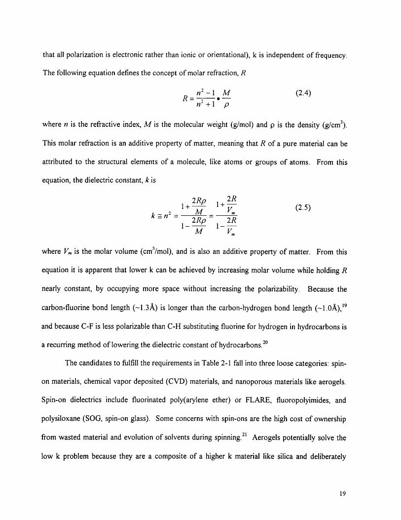
The following equation defines the concept of molar refraction, R
n2 - 1 M (2.4)R- -*-n2 +1 p
where n is the refractive index, M is the molecular weight (g/mol) and p is the density (g/cm3).
This molar refraction is an additive property of matter, meaning that R of a pure material can be
attributed to the structural elements of a molecule, like atoms or groups of atoms. From this
equation, the dielectric constant, k is
2Rp 2R1+-2 1 + (2.5)
k _ n2 M V,2Rp 2R
1- 1-VM V.
where V. is the molar volume (cm 3/mol), and is also an additive property of matter. From this
equation it is apparent that lower k can be achieved by increasing molar volume while holding R
nearly constant, by occupying more space without increasing the polarizability. Because the
carbon-fluorine bond length (-1.3A) is longer than the carbon-hydrogen bond length (-1.OA),' 9
and because C-F is less polarizable than C-H substituting fluorine for hydrogen in hydrocarbons is
a recurring method of lowering the dielectric constant of hydrocarbons. 20
The candidates to fulfill the requirements in Table 2-1 fall into three loose categories: spin-
on materials, chemical vapor deposited (CVD) materials, and nanoporous materials like aerogels.
Spin-on dielectrics include fluorinated poly(arylene ether) or FLARE, fluoropolyimides, and
polysiloxane (SOG, spin-on glass). Some concerns with spin-ons are the high cost of ownership
from wasted material and evolution of solvents during spinning. 2' Aerogels potentially solve the
low k problem because they are a composite of a higher k material like silica and deliberately

incorporated air-filled pores. The dielectric constant of composite materials is a weighted average
of the individual dielectric constants proportional to the volume fraction of each component.
However, there are many manufacturability, structural integrity and reliability issues related to
intentionally fabricating pores in that process.
This paper focuses on CVD deposited materials because of their high manufacturability
and familiarity in the semiconductor industry. CVD processes also have advantages over other
deposition methods in improved adhesion, ability to process larger wafers, 22 higher film density,
and high throughput.23
2.2.2 Ultra Low k Materials
Currently two materials stand out as likely candidates for the next CVD low k dielectric,
parylene-F and fluorinated amorphous carbon (a:C-F). There are many recent papers on both of
these materials, 20' 21,24-27 and several CVD suppliers are developing one or both of these materials
for the next microprocessor generation.
2.2.2a Parylene-F
For almost 30 years, vapor deposited parylenes have been used as coatings for metals
composites, glasses, plastics and elastomers. Figure 2-4 shows the structures of four parylene
variants.

Parylene-N has a low dissipation factor, and has high crevice penetration. Parylene-C has
been used as a moisture barrier, and parylene-D has the best thermal stability of traditional
parylenes.
Parylene-F, which is similar to parylene-N but with fluorine substituted for hydrogen on
the aliphatic carbons, has the highest thermal stability based on the higher bond energy of the C-F
bond compared to the C-H bond.2 9 Parylene-F is deposited from the vaporization and
pyrolization of the dimer cyclodi(a,a,oa',a'-tetrafluoro-p-xylylene) into polymerizable monomer
tetra-olefini para-xylylene. The deposition vacuum chamber is held at or below room
temperature, so that the vapor condenses and polymerizes growing the polymer layer from the
surface of the substrate, conforming to all features. 30
Wary, Olson, and Beach report that parylene-F has a dielectric constant of 2.28, thermal
stability of less than 1% weight loss over 2 hours at about 450TC, and that it "bonds well to all
pertinent surfaces in microelectronic construction.""30 Piano reports a dielectric constant of 2.24
and gapfill of up to 4:1 aspect ratio structures of 0.13 .tm trenches for parylene-F. 31
2.2.2b Fluorinated Amorphous Carbon (a:C-F)
Although polytetrafluoroethylene (PTFE) has one of the lowest dielectric constants of any
fluoropolymer (k-2), its low adhesion strength and thermal stability restrict its integration into the
microprocessor. However, current research on improving PTFE is ongoing in Karen Gleason's
group at MIT using pulsed plasma deposition to reduce ion bombardment during deposition and
improve thermal stability. Contrastingly, hydrogenated amorphous carbon (a-C:H) films have

high thermal stability because of their cross-linked structure, but do not have a low dielectric
constant.
Blending the advantages of each of these materials into one, fluorinated amorphous carbon
(a-C:F) combines the low dielectric constant of a fluorocarbon with the thermally stable structure
of amorphous carbon, while also making use of the existing CVD reactors and gas chemistries
used for plasma etching. Like parylenes, fluorocarbons are used as protective coatings, and also
may require an amorphous carbon base layer to improve their adhesion.3 2
Endo and Tatsumi report a dielectric constant of 2.1 (at 1 MHz) for their films, with no
shrinkage and thermal stability up to 300,C. 32 Theil has attained an amorphous fluorocarbon film
with a dielectric constant of 2.3 with good thermal stability.33 Robles reports that HDP deposited
a:C-F (with amorphous carbon base layer for adhesion) is thermally stable up to 350'C, has a
dielectric constant of 2.7, and has good gapfill of 2:1 aspect ratio gaps; however, an adhesion
layer for sidewalls is required.34
2.3 Graphite Fluoride
There are several articles on fluorinated graphite compounds and fluorinated carbon blacks
that provide some insight into the potential structure of fluorinated amorphous carbon.35-4 The
compounds discussed in these articles are of the form CxF (1<x<30) and are most often formed by
the fluorination of graphite fibers or carbon black under fluorinated atmosphere at elevated
temperatures. One interesting CxF compounds to this study is (C2F),, or poly(dicarbon
monofluoride), which forms a puckered sheet structure at around 350-4000 C and is black in
color.42 Fluorination at even lower temperatures (around 20'C) also produces a black C2F
material, but with a planar sheet structure.43 Although graphite is a conductor, Mallouk and

Bartlett report that the resistivity of CxF (x=1.94) is 2x10 7 Qcm, indicating that this material might
be used as an insulator. 44
(C2F)n in its crystalline form is a sheet structure, the puckered form is shown in Figure
2-5, alternating every other layer of carbon with a layer of fluorine. CF 2 and CF 3 groups
terminate the edges of the layers Although no dielectric constant for the bulk material has been
reported, it is shown that variations in the fluorine treatment of the graphite precursor produce
very different bonding characteristics. In particular, fluorine intercalation compounds can be
produced with a more ionic bond structure, which preserves the sp 2 bonding of graphene, and
alternates layers of semi-ionically bonded fluorine.46
(C F )n
Monolayer of graphite fluoride*: C atom 0: F atom
Figure 2-5: Structure of (C2F)., poly(dicarbon monofluoride). Taken from Watanabe et. al.45

a)
b)
Peak Label C s Binding AssignmentEnergies (eV)
1 284.2 Graphitic C2 285.2 Asymmetric component3 287.0 Semi-ionic C-F bond4 288.71 Covalent C-F bond5 290.6
1 284.1 Graphitic C2 285.1 Asymmetric component3 287.4 Semi-ionic C-F bond4 289.1 Covalent C-F bond
Binding Energy (eV)
Figure 2-6: Cls XPS data from two types of CF with a) more covalent bonding, and b) more ionicbonding.47
Figure 2-6 shows Cls XPS data from CxF (2.2>x>2.8) prepared in two different
environments. The deconvoluted peak 3 indicates the semi-ionic bond (at a binding energy of
around 287eV), and peaks 4 and 5 indicates the covalent CF 2 and CF 3 bonds (at binding energies
of -289eV, -290eV). Nanse et. al report that the semi-ionic C-F bond produces an XPS peak
that is shifted between 2.7 and 3.9 eV from the non-fluorinated C-C bond. The covalently bonded
C-F groups produce XPS peaks shifted greater than 4.4 eV from the non-fluorinated C-C bond. 48
The semi-ionic bonding causes less charge to be distributed to the carbon atoms which may
contribute to the higher Cls binding energy than covalently bonded carbon atoms. 49 This semi-
ionic character is highly desirable for a low k dielectric, because as mentioned above, ionically
bonded C-F should have lower polarizability than covalent bonded C-F. In fluorinated graphite
and carbon blacks, the character of the bonding is dependent on the temperature at fluorination,
the source of fluorine used for fluorination, and the structure of the starting material.50
The (C2F)n structure provides another desirable quality for interlayer dielectrics, thermal
stability. Watanabe reports that in vacuum (C2F)n is stable up to 590TC." Although the
fluorinated carbons investigated for low k dielectrics in this study are amorphous, it is possible the

CxF fluorinated graphites provide a structural model for obtaining low k while maintaining the
high thermal stability required of an ILD.
CHAPTER 3. EXPERIMENTAL PROCEDURES AND METHODS
3.1 Sample Description
All the dielectric films discussed in this report were thin films, 0.5 Itm -2 p.m in thickness,
deposited on silicon substrates. Table 3-1 lists the wafer substrates used in this study as well as
the type of experiments run on each type of substrate. The film deposition processes are
proprietary to Intel Corporation, as are the doping levels of the wafer substrates.
Table 3-1: Types of wafer substrates and their uses in this study.
Substrate Wafer type Doping ExperimentationBare Si lightly doped p-type Adhesion, thermal stability,
metal-insulator-semiconductor electricalcharacterization, surface andbulk structure/compositionanalysis
Bare Si heavily doped p-type (metal-insulator-metal)-likeelectrical characterization
Bare Si low oxygen p-type infrared spectroscopy1000A SiO2 on adhesionBare SiBlanket (same as Bare Si, lightly doped } metal-insulator-metalAI-0.5%Cu film electrical characterization,on Bare Si adhesionTopographic gapfill, shrinkage/adhesiontest devicewafer
Three different types of fluorinated amorphous carbons were investigated, two from two
different types of high density plasma enhanced CVD reactors-referred to as HDP-1 and HDP-2
for the remainder of this paper-and one from a lower density plasma enhanced CVD reactor-
referred to as PECVD. The HDP- films have been examined both in the as deposited form, and
after an in situ anneal by exposure to an argon plasma prior to removal from the deposition

chamber. Many experiments were performed on films that had been annealed at 4000 C for
various durations in either N2 or He ambients. For comparison, pulsed plasma PECVD deposited
PTFE films from Professor Gleason at MIT also underwent some of the characterization
The following matrix (Table 3-2) shows the experiments performed in this study. Because
this work was done in an industrial setting, all experiments could not be done on all of the
materials, rather, select experiments were done to detect trends and provide feedback for the
materials development.
Table 3-2: Experiment matrix.
FTIR XPS NMR TGA TDS Adhesion k
Parylene-FPECVD a-C:F * * *Annealed PECVD a-C:FHDP-I a-C:FAnnealed HDP-1 a-C:FHDP-2 a-C:FAnnealed HDP-2 a-C:F *Pulsed Plasma PTFE * * 0 *
3.2 Compositional and Structural Analysis
Several spectroscopic techniques were used to determine the composition and structure of
the materials. Fourier Transform Infrared spectroscopy (FTIR) was the preliminary structural
analysis technique, primarily used to discern structural changes caused by annealing at various
temperatures. X-ray Photoemission Spectroscopy (XPS) provided information about the
bonding state of the elements, but is limited to surface analysis only. Auger Electron
Spectroscopy (AES) depth analysis was used to provide further information about the
composition of the bulk of the film. '9F Fast Magic-Angle Spinning (MAS) Probe Nuclear

Magnetic Resonance (NMR) spectroscopy was used to obtain additional bonding state
information on the films.
3.3 Thermal Stability
3.3.1 Thermogravimetric Analysis (TGA)
The first of the two thermal stability analysis techniques used in this project is
Thermogravimetric Analysis, or TGA. This method is used to determine the weight percentage of
the film that is lost at elevated temperatures."3 Figure 3-1 shows a schematic of the Cahn TG 131
from TGA test apparatus from ATI Instruments used in this experiment. This equipment has a
weight loss sensitivity of 0.1 pg to 1 pg.
nAI AfArC SV4Rai A N C'I
VACUUMCONNECTION
Figure 3-1: TGA test apparatus."4
In TGA, approximately 1cm 2 pieces of wafers deposited with the low k film of interest are
placed in a quartz crucible. The crucible is suspended from a microbalance by a nickel chromium
alloy wire and counterbalanced by an empty reference sample holder. The sample is placed in a
furnace that is continuously purged with helium.
FURNACEAIR

The sample weight is continuously monitored as the sample is ramped (10oC/min) from
55oC to 4250 C and then held at 425°C for two hours. Subsequently, the sample is heated to
800NC and held for two hours to decompose all of the film from the substrate (See Figure 3-2).
The sample is put through this procedure twice. The second run is used as a baseline and is
subtracted from the first run to eliminate buoyancy effects. The thermal stability is measured in
terms of the percentage of film weight lost over two hours at 4250C. The percent weight loss
over two hours is calculated as the ratio of the weight lost during the 425oC isotherm to the total
weight lost after the film is completely burnt off at 800TC.
3.3.2 Thermal Desorption Spectroscopy(TDS)
Although the amount of film lost at elevated temperatures is important, an additional
assessment technique for thermal stability is necessary because the low k dielectric films are
fluorinated. Even if the relative amount of decomposition is low, the composition of the
outgassing species is critical. Fluorine can cause metal corrosion and/or etch SiO 2.

Thermal Desorption Spectroscopy, or TDS,55 was used to identify and characterize the
outgassing at elevated temperatures using a Ruska Thermex Pyrocell, and a Hewlett Packard
5972 Series Mass Selective Detector. Approximately Icm x 4cm pieces of wafer deposited with a
low k dielectric film were places in a quartz sample holder inside a furnace. The furnace is purged
by helium gas which carries the outgassing material through a heated quartz line-to reduce
deposition on the chamber walls-to a mass spectrometer, as shown in Figure 3-3.
A diagnostic blank run is performed before every new sample. The empty sample holder
is ramped to 650'C and held for 25 minutes to clean any residual material from the sample holder
as well as to purge the system. In addition, the inherent equipment background in the system is
monitored by this clean run to establish that the equipment is operating correctly. This
background is subtracted off of the raw data to isolate only the materials that evolve from the
sample.
)QOor ,5i02 He
SampleHolder
He mI
Figure 3-3: TDS test apparatus. Samples are heated in the furnace. Outgassing material is carried byHelium purge gas through a gas chromatograph (not used) and into the mass spectrometer.

One issue that arises when studying fluorinated materials in this system is that outgassing
fluorine reacts with the quartz sample holder and chamber walls and forms SiF 4 which is detected
in the form of SiF 3'. Detection of mass 85, SiF3', indicates the outgassing of fluorine or HF.
3.4 Adhesion
Several wafers were tested using a Sebastian I or a Sebastian V Adherance Tester. Fifteen
samples are taken from each wafer. The samples are approximately lcm2 pieces with
perpendicularly attached epoxy coated aluminum nail shaped studs from QuadGroup. The
samples are placed in an oven for a 50 minute epoxy cure at 1500 C prior to stud pull testing.
After cooling to room temperature, the samples were tested by applying a controlled pull force to
the stud until the film failed and the stud detached from the wafer sample.
3.5 Electrical Characterization
Dielectric constant was measured from CV measurements. Two capacitor structures were
used for these tests, metal-ILD-semiconductor (MIS), and metal-lLD-metal (MIM). To create
MIS capacitors, metal dots were sputtered through a mask onto a dielectric film on a silicon
substrate. To create MIM capacitors, the metal dots were sputtered onto a dielectric film on a
blanket metal film coated silicon substrate. Alternately, heavily doped silicon substrates were also
used to simulate the behavior of a metal and obtain MIM-like CV curves. The details of the metal
layers' composition is proprietary to Intel Corporation.
A DC bias is swept over the voltage range of interest and the capacitance is measured at a
certain frequency (typically 1MHz). The metal-ILD-semiconductor capacitor can be modeled as a
two parallel plate capacitors in series. When the system is biased into the accumulation region,

the total capacitance is taken to be the capacitance of the dielectric, because the serial capacitance
1/Ccq=/C, +I/CrD is dominated by the dielectric film capacitance. In a metal-ILD-metal
capacitor only the capacitance of the ILD is measured.

CHAPTER 4. RESULTS AND DISCUSSION
4.1 Compositional and Structural Analysis
Figure 4-1 shows the Fourier Transform Infrared (FTIR) spectra for parylene-F. There
was some change in the FTIR spectrum after anneal for 5 minutes at 1500 C in N2 ambient, most
notably the increase of the peak at approximately 810 cm-', but then the film stabilized and did
not show any further change in spectrum even after 24 hours at 1500 C (not shown). After an
anneal at 300'C, additional change in the FTIR spectrum was observed, including the reduction
of the peaks on either side of the peak at -1260 cm-' and those on either side of the peak at 900
cm l'. The lack of comprehensive reference literature makes accurate identification of the peaks
difficult, however, some preliminary identifications are presented here.53
C anneal
s dep
Lo
0((U.00
u,.
800 700 600
Wavenumber (1/cm)
Figure 4-1: FTIR spectra for parylene-F as deposited and after annealing.
1600 1500 1400 1300 1200 1100 1000

The region from 1300-1000 cm-' is the C-F stretch region for aliphatic fluorinated
compounds. After annealing, the peak around 1270 cm-' lost its shoulders and became more
narrow, which may be explained by the loss of some CF 2 during anneal. The region from 900-
650 cm-' is related to CH deformation in aromatic compounds. Comparison between the FTIR
spectra for the monomer, dimer and the pre- and post-annealed film suggests that loss of dimer
may cause the diminishing of the shoulder at -840 cm ~' and of the small peaks at -940 cm'.
Further work is required to fully identify these peaks.
The FTIR spectra for two pulsed plasma PTFE samples are shown in Figure 4-2 for
reference. Spectrum 4-2(a) shows the FTIR of the film with a longer pulse off time. Less ion
bombardment during pulse off time allows long lived neutrals to deposit with less damage
creating a fluorocarbon film that is more PTFE-like. 56 The peak assignments are taken from
d'Agostino et. al.57 The peaks at 1160 cm-' and 1220 cm-' represent the symmetric and
asymmetric CF 2 stretches. There is a slight shoulder caused by the 1340 cm-' CF stretch. Also
seen in this spectrum is a very weak CF3 band at approximately 980 cm-'. The highly resolved
CF 2 peaks indicate that this film has a predominantly CF 2 structure.

The FTIR spectrum for an amorphous PTFE thin film, shown in spectrum 4-2(b), has the
characteristic strong band in the 1300-1000 wavenumber region, however, the high disorder of
this film causes line broadening and overlap of neighboring bands, and the resolution of the CF2
peaks disappears. This spectrum also shows a broad band between 1650 and 1800 cm'. There
may be contributions from C=O (1720 cm-) due to water or oxygen incorporated into the film
and/or unsaturated carbon-carbon double bonds (1780 cm-').
A comparison of the HDP-1 and HDP-2 fluorinated amorphous carbon films both before
and after anneal is shown in Figure 4-3. Again, the same CF, CF 2, and CF 3 bands appear, as well
as some C=C, and C=O. The broadness of the C-F band and the largely unresolved peaks
indicate that these films are disordered. The large CF shoulder suggests that the films are highly
CF 2 1160cm ~', 1220cm-'
d
E
(I
0E
.t0(I)< b.04C
2000 1800 1600 1400 1200 1000 800 600
Wave number (1cm)
Figure 4-2: FTIR spectra for Pulsed Plasma PECVD PTFE films developed by K. Gleason at MIT, showingcharacteristic peaks in C-F region. Spectrum (a) is 10/400 on/off pulse time (more PTFE-like), (b) is 10/20on/off pulse time (more disordered).

cross-linked. The C=O band at 1720 cm -' decreased slightly after anneal, indicating that oxygen
is lost from the film during annealing.
Figure 4-3c, which shows the spectrum of the HDP-1 film after an in situ anneal, does not
show a reduction of the peak at 1720 cm-', although Figure 4-3d and 4-3d, which show the
HDP-1 and HDP-2 spectra after oven anneals, do show loss of the C=O peak at 1720 cm-'. It is
apparent that the in situ plasma anneal performed immediately after deposition for the HDP-1
film is not comparable to an oven anneal for 30 minutes at 4000 C for reducing the C=O band.
Interestingly, despite having different precursor gases and different CVD reactor types, there
appears to be little discernible difference in FTIR spectra between the two materials after
annealing for 30 minutes at 4000 C.
C-F
So
r.00u).0
3900 3400 2900 2400 1900 1400 900 400
Wave num ber (1/cm)
Figure 4-3: FTIR spectra of amorphous fluorocarbon thin film dielectrics for various pre- and post-annealed samples. a) HDP-1 as deposited, b) HDP-2 as deposited, c) HDP-1 after in situ plasma anneal, d)HDP-1 after 4000C anneal in N2 ambient, e) HDP-2 after 400*C anneal in N2 ambient.

X-Ray Photoelectron Spectroscopy, XPS, was done on some of the samples to give
surface structure information on the materials." The deconvoluted peaks give an estimation of
the percent of carbon atoms in each bond environment. Some spectra were modeled with five
peaks and some were modeled with four peaks typically spanning 2 to 4 eV each. In the spectra
that were modeled with five peaks, the two lowest binding energy peaks (-287 eV and -289 eV),
represent the non-fluorinated C-C bond and the C-C-F bond (non fluorinated carbon in the
presence of fluorine), respectively. In the spectra modeled with only four peaks, the C-C and the
C-C-F regions are grouped together into one peak meaning that the lowest binding energy peak
represents both types of non-fluorinated carbon moieties. The samples for this experiment were
taken before and after Thermal Desorption Spectroscopy, so the anneal for these samples
consisted of a 10oC/min ramp to 4000 C and a 25 minute hold at 400TC in helium ambient.
Figure 4-4 shows the XPS C Is spectrum from an as deposited HDP-2 sample, with an
inset of the XPS of (C2F),, for comparison, showing that HDP-2 amorphous fluorocarbon has
very similar XPS results to (C2 F)n. The difference in absolute binding energy is due to different
charging effects between samples. The peak at 290.9 eV is a semi-ionic C-F bond (3.6eV shift
from C-C bond). The peaks at higher binding energies are covalently bonded (greater than 4eV
shift from C-C bond).

kCP6
')Q'7 '2za
C-CI
Figure 4-4: Cls XPS results for as deposited HDP-2 amorphous fluorinated carbon film. Inset is Cls XPSspectrum of (C2F). (Taken from Watanabe et. a155).
The amorphous fluorocarbons were all deposited at temperatures around 3500C to 4000C.
The HDP-2 films were particularly black in color, although all of the standard fluorocarbon
deposition techniques produced dark films. These XPS results suggest that the amorphous
fluorocarbon films are C2F-like, although only surface information can be inferred from the XPS.
XRD and TEM results verify, however, that the films have no crystallinity down to 2 nm
resolution.
__· _ ____ _
r P
.i?w 2M M

Figure 4-5 shows the XPS Cls spectrum from an as deposited modified HDP-2 process
that produced a more transparent film. The semi-ionic C-F peak (peak C at -291 eV) is much
larger for this sample than for the standard HDP-2. This sample may have more semi-ionic
bonding, causing less polarizability and possibly a lower dielectric constant. This material was
not submitted for dielectric constant measurements because sufficient material was not available,
but future work on this recipe should include dielectric constant measurements.

0.7
c 0.6
43 0.5 X CF3
SCF2c 0.4 CF2Or jCF- 0.30 A
o 0.2 4
0- X x
0g O C O. a _
Figure 4-6: Bond type concentrations calculated from the area under deconvoluted peaks in XPS Cls data.
Figure 4-6 is a plot of the relative amounts of each bonding state before and after anneal
for three samples, PECVD, HDP-2, and the modified HDP-2 (called HDP-2*) amorphous
fluorocarbons. Contributions due to extrinsic carbon surface contamination introduce some error
in the estimation. This plot shows that after anneal, the percentage of non-fluorinated carbon
bonds always increases, the percentage of C-F bonds decreases, and the percentage of CF 3 bonds
slightly increases. The modified HDP-2* sample shows a drop in the percentage of CF 2 groups
as well. These results suggest that more fluorine is lost than carbon during annealing, which
contributes to the increase in C-C bonding.
XPS surface measurements and Auger Emission Spectroscopy (AES) depth profiles were
both used to determine the composition of the films before and after anneal, and the results are
shown in table 4-1. The primary components were carbon and fluorine, although a few percent
of oxygen and nitrogen were detected in all of the samples. The surface concentration
measurements are comparable between the two techniques. Table 4-1 shows that for PECVD
fluorocarbon, the C/F ratio increases after anneal, as predicted by the Cls spectra. AES shows
40

that the bulk carbon concentration is slightly higher than the surface concentration, but whether
this is an artifact of the XPS, a result of exposure to the environment, or a true representation of
structure cannot be determined.
Table 4-1: XPS and AES composition results.
Sample XPS (surface AES (surface AES (bulkconcentration) concentration) concentration)
PECVD as dep C, 75F C1. 78F C2.6FPECVD after anneal C2.2F C2.2F C2.6FHDP-2 as dep C3 5F
HDP-2 after anneal C4F
Fast Magic Angle Spinning Nuclear Magnetic Resonance (MAS NMR) Spectroscopy
was used to obtain further insight into structure of the bulk of the films. The spectra were
recorded at the fluorine excitation frequency of 254 MHz and referenced to the PTFE CF 2-CF 2
peak with respect to the accepted standard CFC13 (-123.7ppm). 59 Figure 4-7 is the '9F MAS
NMR spectrum for the parylene-F sample, showing both the actual and the sideband suppresed
spectra. The spinning sideband suppression program is used to differentiate the isotropic peaks
from the spinning sidebands which are artifacts of the experiment. The sideband suppressed data
is not used when peaks are integrated.

NMR Spectra for Parylene-F
The NMR spectra of the two parylene-F samples (one on bare silicon, one deposited on
an adhesion promoting layer) looked identical; both showed only the CF 2-CF 2 peak which is to
be expected with parylene-F (CF,-benzene-CF 2)n. After annealing, however, there was a slight
narrowing of the peak which may indicate that some re-ordering and/or loss of CF 2 occurs during
anneal.
Figures 4-8 and 4-9 show the NMR spectra for the PECVD and for the HDP-2
fluorocarbon samples before and after anneal. The peak assignments are given, 59 but because the
bands are so broad, the spectra are broken down into four regions: (CF-), (CF 2-CF 2), and
(CF 3-CF 2) and (CF3-) other bond environments for quantification.
Non-suppressed
bediS- and su
ppressed
-100 -200 -300 -400200 100
ppm
Figure 4-7: "'F NMR Spectra for parylene-F sample (arbitrary units on y axis). Upper spectrum indicates theisotropic data; lower spectrum is slightly offset to indicate the spinning sideband suppression program usedto identify spinning sidebands and avoid classifying them with chemical shifts. The single peak at -120 is theCF2-CF 2 peak.
Sideand upprsse

'-- I
1CF3 I
50 0 -50 -100 -150 -200 -250 -300
ppm
Figure 4-8: "'F NMR results from PECVD fluorocarbon, normalized by weight and number of scans. Theblack shows the results from the as deposited sample; the grey shows the resu Its after a 400*C anneal. Thedeconvoluted peaks are shown for the as deposited sample.
-- PECVD as dep
----- PECVD annealed
-- CF3
-- -CF3-CF2
.. .- CF2-CF2
-- CF

ICF,- I
The spectra in Figures 4-8 and 4-9 are normalized by the weight of the sample to allow
comparison before and after annealing. The area under the curve of the spectra is directly
proportional to the amount of fluorine present in the sample. Therefore, the percentages of the
four bond environments for the materials can be calculated, as shown in Figure 4-10. These
results show that for all three amorphous fluorocarbon materials, the C-F bond group is the most
abundant type of carbon fluorine group. The high percentage of C-F bonds supports the theory
of a short range non-crystalline C,F-like film structure.
HDP-2 as dep
------ HDP-2 annealed
-- CF3
-- CF3-CF2
..... CF2-CF2
-- CF
CF 2-CF 2
I I I II I
0 -50 -100 -150 -200 -250 -300
ppm
Figure 4-9: "9F NMR spectra for HDP-2 fluorocarbon normalized by weight and number of scans. The blackline shows the results from the as deposited sample; the grey diamond line shows the results after a 4000Canneal. The deconvoluted peaks are shown for the as deposited sample.
i I

I I I I I I I I
4 IV'~OL -Ivu~ - - m m 5' I,
90 - I I
00 CF3* CF3-CF20 CF2-CF2I CF
PECVD PECVD HDP1 HDP1 HDP2 HDP2annealed annealed annealed
Figure 4-10: NMR data broken down into percentages of carbon to fluorine bond types calculated by curveintegration.
- i-
NMR results for different deposition recipes for the HDP-2 films were very similar, so it is
evident that small process variations do not significantly alter the structure of the film. The
different deposition reactors and precursor gases for the PECVD and HDP-2 amorphous
fluorocarbon produce materials with reasonably similar structures, although some variations are
noted between materials. The PECVD and HDP-1 fluorocarbons have slightly more CF- bonding
(suggesting that the PECVD and HDP-1 films may be more graphite fluoride-like than the HDP-2
films), and slightly less CF 3 bonding, but the NMR results are otherwise very similar.
The NMR data shows some CF 3- content (approximately 10-15%) for all the samples,
which suggests a possible thermal stability issue. The presence of CF3 groups can contribute to
thermally activated outgassing in fluorinated amorphous carbons; the CF3 side chains are easily
evaporated during heating. All of the fluorocarbon films show outgassing of CF 3 at 400'C in
thermal desorption spectroscopy.
Annealing caused a slight change in the distribution of bond states towards higher CF3-
content, as can be seen in Figure 2b as well. This result is interesting since the CF 3 outgassing
45
I~----..---- ---C·--~~---- _- _ - --- _ _ I I _-~---·~__- ___-_rs
90% -
80% -
70% -
60%
50% -
40% -
30% -
20% -
10% -
0% - I - it
I I
i

declines significantly if TDS is repeated on a sample that has already cycled through a ramp to
400'C and held for 25 minutes in its first TDS run. Apparently the CF 3 remaining after an anneal
is significantly more stable. The increased resolution of the CF 3CF 2- peak (smaller peak in the
CF 3- region in Figure 4-8 and 4-9) may be linked to this increase in CF 3 stability.
4.2 Thermal Stability
4.2.1 TGA
TGA results for the thermal stability of various films over a two hour isotherm at 4250 C
are shown in Table 4-2. In comparison, CVD deposited SiO 2 has less than 1% weight loss during
the same isotherm." Although weight loss at 4250 C is a sufficient technique for establishing the
thermal stability of SiO 2, more information is needed for the fluorinated organic dielectric
materials.
Table 4-2: Summary of TGA results for several dielectric films.
Sample %Weight Loss during2 Hour 425°C Isotherm
Parylene-F 0.5As Deposited HDP-1 (a-C:F) 1.4
Annealed HDP-1 (a-C:F) 1.9HDP-2 (a-C:F) 6.3-8.9
It is possible to detect weight loss during the ramp to 4250 C using TGA, and one example
is shown in Figure 4-11. Although the parylene-F shows low weight loss during the 425°C
isotherm, there is a weight loss of about 10% during the ramp between 150'C and 250TC.
Because the TGA method bums off the film completely, it is impossible to tell from TGA whether
this low temperature weight loss would repeat if the sample were cycled up to 425oC again. In
46

addition, TGA does not give any information on the composition of the outgassing material.
Because the low k dielectrics are fluorinated, there is a risk of fluorine and HF outgassing that can
interact with metal layers, cause corrosion, or etch SiO 2. Characterization of the outgassing can
be done more thoroughly using Thermal Desorption Spectroscopy.
4.2.2 TDS
Figure 4-12 shows the TDS Total Ion Count (a sum of the abundance of all ions counted
outgassing from the sample) for a parylene-F sample. The scan for the first heating cycle shows
the results from a sample that was heated to 400TC and held for 25 minutes. Unlike the TGA data,
TDS data indicate that the temperature for the initial release of material is approximately 250TC.
Both the TGA and TDS methods described in this report have dynamic temperature ramps over
the outgassing temperatures, so the actual outgassing temperature cannot be determined. The
components of the outgassing peak between 2000 C and 350TC during the ramp were
o 102 -
.E 100S98
, 96E
94 -
5 92-
S90-
,_ 88-S86 -84 8 i 4 I I
0 100 200 300 400 500
Temp (C)
Figure 4-11: TGA graph showing weight loss during temperature ramp for parylene-F. There is a 10%drop in film weight between 150"C and 250"C.
rnA

predominantly monomer, dimer, and their fragments. No fluorine (mass 19), HF (mass 20), or
SiF3 (mass 85) that would indicate the presence of HF were detected.
1.2 1
11
81
61
41
21
0 10 20 30 40Time (min)
450
400
350
300
250
200
150
100
50
--- 1st Heat Cycle-G- Second Heat Cycle
50 60 70
Figure 4-12: TDS results for parylene-F. The sample was rampedconsecutively without exposure to air between runs. Background isbackground level is not detected in second run.
to 400*C and held for 25 minutes twiceincluded to show that outgassing above
The second heating cycle on the same sample without exposure to the environment or
opening of the sample chamber showed no outgassing above the equipment background level.
This indicates that a 400TC anneal of 25 minutes is sufficient to make the film thermally stable up
to 400TC. Additional experiments are in progress to determine the upper limit of the thermal
stability of annealed parylene-F.
When tested in TDS, no pulsed plasma PTFE film remained after the first heating cycle,
which means that it is not stable at 400TC. The pulsed plasma PTFE began to outgas at
approximately 125TC and was completely burned off after less than five minutes at 4000C.

Representative TDS results for the amorphous fluorocarbons are shown by the two
examples in Figure 4-13. All of the amorphous fluorocarbon materials showed low temperature
outgassing as well as continued outgassing during the 400'C isotherm during the first heating
cycle, but as shown by TGA this loss is less than 10% by weight. The low temperature
outgassing for the HDP-2 samples (with several process recipe variations) all showed a total ion
count peak between 100oC and 300TC. The main component was mass 69. This indicates that
some highly volatile CF 3 desorbs from the material early in the temperature profile. CF 3
outgassing is also seen at higher temperatures which may be the result of the decomposition of the
material into CF 3 fragments. The low temperature outgassing peak also contains masses 43, 57,
and 71 which have been tentatively identified as C2F, C2FN, and C2FN 2, although a mechanism for
their formation cannot be determined. These species are seen only in the initial peak between
100C and 300TC.

1.2
1
0.8
o 0.6
80.4
0.2
0
450
400
350
300
2501-
200
150 -- PECVD (a-C:F) 1st cycle-- PECVD (a-C:F) 2nd Cycle
100 - - HDP-2 (a-C:F) 1st Cycle+ HDP-2 (a-C:F) 2nd Cycle
0 10 20 30 40 50 60 70
Time (min)
Figure 4-13: TDS data for first and second heat cycles of PECVD and HDP-2 amorphous fluorocarbon films.The ion counts are plotted as a fraction of the maximum of each curve for comparison from material tomaterial. (Results are shown after background subtraction,)
After a second heating cycle, these materials showed no outgassing below about 350TC,
but the film continued to decompose throughout the isotherm at 400TC. So for the amorphous
fluorocarbons, a 400TC anneal stabilizes the film only up to approximately 350TC. In one
experiment, a sample received four consecutive TDS runs and material continued to outgas at
400TC in the last run, although the total amount of outgassing decreased with each successive
temperature cycle.
Figure 4-14 shows the first cycle TDS results for an HDP-2 film broken down into
individual ion counts. Although each fluorocarbon film with a different process deposition recipe
had slightly different TDS spectra, the HDP-2 sample shown below is representative of most of
the films. Mass 18, 28, and 44 (identified as water, N2 or CO, and CO 2) began outgassing
immediately (around 50°C-100°C). Because mass 28 and 44 always have the same curve shape,
mass 28 is considered to be CO rather than N2 .

It appears that water or 02 incorporated during the deposition, sorbed during exposure to
the atmosphere, or provided by interaction with the SiO 2 chamber walls provided the oxygen seen
in the evolving species of CO and CO 2. In a previous experiment using the same TDS apparatus
on a fluorinated organic polymer Mook and Pan showed SiF 3 outgassing but showed no CO 2,
CO, or water in the spectra.6 0 Leak checks on the TDS equipment verify that there was no
detectable source of oxygen leaking into the system. Therefore, the oxygen source appears to be
in or on the film itself. The fact that carbonyl is lost during anneal, shown by FTIR, supports this
hypothesis.
0 10 20 30 40 50 60 70
Time (min)
Figure 4-14: TDS results from the first heating cycle of HDP-2 amorphous fluorocarbon film, broken downinto individual ions. Note that CO and CO2 begin to outgas at very low temperatures, and that SiF 3 is notdetected until around 200'C.
Mass 20 (HF) and 85 (SiF 3) evolved between 2000C and 3000C, peak at 4000 C and
dropped off. Water in the film may be providing the hydrogen for this HF/SiF 3 formation as well.
Several CxFy ions were detected, although only CF 3 is shown in Figure 4-14.
L.0 IU
2 104
1.51040Oa 1 10 4
5000
4VU
400
350 * Water300. 30 HF
300 I CO250 E 0 CO2
A CF3200 + SiF3
150
100
4

Certain ions were observed to peak slightly before the CxFy ions. To accentuate this peak
difference and exaggerate the temperature gradient between the set temperature and the sample
temperature, an HDP-2 sample was run through TDS with a 500C ramp to 4000 C. All other
parameters of the Mass Spectroscopy method remained the same. The results of this experiment
are shown in Figure 4-15. The time at which ion 69 (CF 3) reached its maximum was significantly
different from the rest of the ions. This is true for other CxFy fragments as well.
Figure 4-15: TDS data for HDP-2 sample with 50°C/min ramp to 400"C. The two vertical lines show theshift between the peak time for water, HF, SiF 3, and CO2 and the CF,y components represented here by CF3.
Table 4-3 lists the most commonly detected masses for the fluorocarbon films categorized
as those that peak earlier (possibly related to the presence water or oxygen) and those that peak
slightly later due to the decomposition of the CxFy structure of the film. The grouping of these
outgassing ions supports the two mechanisms suggested for film degradation mentioned above.
Water provides oxygen that evolves in CO and CO 2 from the film, and hydrogen that forms HF
with evolving fluorine. The HF (mass 20) formed attacks SiO 2 in the walls of the chamber or on
61
51
41
0o31
S21
11
400
350
300 j -0 WaterC -E- HF
250 E0 C02
200 -- CF3150 -~ SiF3
150
100
50

the substrate forming SiF 4 which degrades entirely into SiF 3 (mass 85). The CxFy decomposition
is not directly related to the presence of water in the film.
Table 4-3: Identifications of commonly detected ion masses from TDS data of amorphous fluorocarbons.
Earlier PeakM/Z Identification18 water20 HF28 CO85 SiF344 CO 2
7181100119131169
The thermal decomposition data during the ramp to 400'C can be plotted in an Arrhenius
plot of the natural log of the ion counts versus the inverse of the temperature. Figure 4-16 is a
graph of the slopes for different ions and different deposition conditions. The slopes cluster for
each ion emphasizing again that the materials are very similar despite differences in processing.
After annealing the slopes increase, indicating that there is a larger resistance to decomposition
after the sample has undergone a thermal cycle.
Later PeakIdentificationCFC2FCF2
CF2HC2FN
M/Z3143505157
CF 3
C2FN2C2F3C2F4C2F5
C3F5
C3F7

OHDP-2
O HDP-2'
A PECVD
X HDP-2 annealedKPECVD annealed
Arrhenius Plot Slopes fromThermal Decomposition
0UUUU
15000
10000
5000
28 44 69
Ion Mass
Figure 4-16: Slopes from Arrhenius plot of thermal decomposition during ramp to 400"C for amorphousfluorocarbon films.
A empirical fit of the data during the isotherm shows that there is a better fit when the data
is plotted as ion counts versus the inverse of time at 400'C than as the natural log of the ion
counts versus time. The purpose of this model is to estimate the anneal time required to bring
outgassing at 4000 C down to zero. For example, the PECVD film will require a 34 hour anneal at
400'C to bring the outgassing total ion count down to zero. Future work in this project involves
determining the reason for this unexpected curve fitting result and improving the model to better
predict the required anneal time to stabilize the films.
The TDS results shown in Figure 4-17 show the outgassing ions from the second heat
cycle of an HDP-2 sample. CO 2 dominates, water and CF 3 continue to outgas and HF is just
above the noise level. Most of the other CxFy species are not observed in the second heat cycle.
If the CO2, CO, and water were eliminated, then CF 3 desorption would be the primary mechanism
of outgassing after a 25 minute anneal at 4000 C for the amorphous fluorocarbons.

3500
3000
2500
2000
1500
1000
500
-500
-5000 10 20 30
Time
results of Run B of HDP-2
450
400
350
300 0,
250 E
200
150
100
5070
3 WaterElHF+ C02o CF3
amorphous fluorocarbon film, broken down into individual
40
(min)
50 60
4.3 Adhesion
The adhesion strength, measured by stud pull, of the various films is shown in Table 4-4.
Films deposited on thermal oxide were adopted as the standard adhesion test samples because
thermal oxide substrates are easy to produce and the adhesion of these low dielectric constant
films to SiO 2 is considered more relevant than adhesion to silicon.
Table 4-4: Adhesion strength of low k films.
As Deposited Annealed FilmFilm (kpsi) (kpsi)
Thermal Oxide on Silicon 8PECVD (a-C:F) 4.06 5.9HDP-1 (a-C:F) 6.82 4.67HDP-2 (a-C:F) 5.37Pulsed Plasma PTFE 0Parylene-F 0
* -
Figure 4-17: TDSions.
:11~~11111111111111 1111111111111111
)
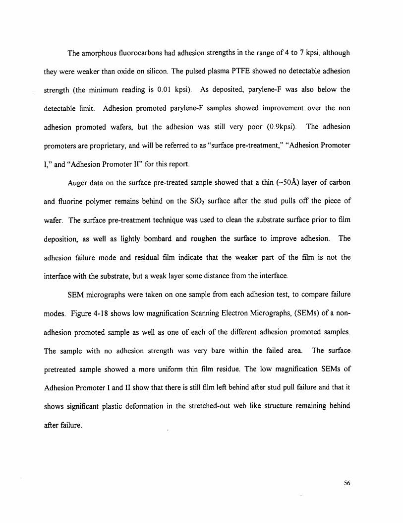
The amorphous fluorocarbons had adhesion strengths in the range of 4 to 7 kpsi, although
they were weaker than oxide on silicon. The pulsed plasma PTFE showed no detectable adhesion
strength (the minimum reading is 0.01 kpsi). As deposited, parylene-F was also below the
detectable limit. Adhesion promoted parylene-F samples showed improvement over the non
adhesion promoted wafers, but the adhesion was still very poor (0.9kpsi). The adhesion
promoters are proprietary, and will be referred to as "surface pre-treatment," "Adhesion Promoter
I," and "Adhesion Promoter II" for this report.
Auger data on the surface pre-treated sample showed that a thin (-50A) layer of carbon
and fluorine polymer remains behind on the SiO 2 surface after the stud pulls off the piece of
wafer. The surface pre-treatment technique was used to clean the substrate surface prior to film
deposition, as well as lightly bombard and roughen the surface to improve adhesion. The
adhesion failure mode and residual film indicate that the weaker part of the film is not the
interface with the substrate, but a weak layer some distance from the interface.
SEM micrographs were taken on one sample from each adhesion test, to compare failure
modes. Figure 4-18 shows low magnification Scanning Electron Micrographs, (SEMs) of a non-
adhesion promoted sample as well as one of each of the different adhesion promoted samples.
The sample with no adhesion strength was very bare within the failed area. The surface
pretreated sample showed a more uniform thin film residue. The low magnification SEMs of
Adhesion Promoter I and II show that there is still film left behind after stud pull failure and that it
shows significant plastic deformation in the stretched-out web like structure remaining behind
after failure.

Figure 4-19 shows higher magnification SEMs (1800x). In order of increasing adhesion
strength, the samples showed increased feature sizes in the plastically deformed region. This web-
like, stringy structure is on a larger scale with each successive adhesion strength improvement,
indicating that the more strongly adhered ultra thin film near the interface may be getting thicker
and stronger.

Figure 4-19: Higher magnification scanning electron micrographs of failed parylene-F stud pull interface, a)Surface pre-treated, 1800xr, b) Adhesion Promoter I, 1800x, c) Adhesion Promoter HI, iSO0x.
4.4 Electrical Characterization
Table 4-5 shows the dielectric constants of each type of material. The dielectric constant
for pulsed plasma PTFE was calculated from the capacitance/voltage curve of a MIS structure
and found to be 2.15. The in-plane dielectric constant for parylene-F was determined by
measuring the 100 kiHz capacitance on a 0.6 micron comb structure. The dimensions of the
structure and the capacitance measurement were used in a model to find the dielectric constant to
be 2.37 +1- 0.13. This is slightly higher than the out of plane dielectric constant at 10 GHz of
~i~P- (

2.25+/- 0.23 measured on a Hg probe. The dielectric constant of the amorphous fluorocarbon
materials was approximately 2.4 measured on MIM structures.
Table 4-5: Dielectric constant for each type of film.
Sample kPulsed Plasma PTFE 2.15 at 1 MHzParylene-F 2.25 at 10GHz (out of plane)
2.37 at 100kHz (in plane)a-C:F -2.4 at 1MHz
Figure 4-20 shows the capacitance of various films at different frequencies. There appears
to be little variation over this frequency range, but a full characterization of dielectric constant at
higher than 1MHz and lower than 1 kHz is required, as it was not available for this study.
500
400 X HDP-1 as dep
A A ý )HDP-1 annealedS300
SHDP-2 as depS200 - X X HDP-2 annealed
1 AParylene-F100
0 !
1kHz 10kHz 100kHz 1MHz
Frequency
Figure 4-20: Frequency dependence of capacitance for various low k dielectrics.

CHAPTER 5. CONCLUSIONS AND RECOMMENDATIONS
CVD deposited thin film materials can achieve the low dielectric constant required by the
sub-quarter micron microprocessor generation (k<2.5). However, there are additional challenges
to be met before a material can be incorporated into an integrated circuit.
Pulsed plasma PTFE has the lowest dielectric constant of the materials measured,
however, it's adhesion is very low. Future work should include the full characterization of the
thermal stability of pulsed plasma PTFE to establish the amount of material lost during the anneal,
as well as adhesion improvements.
Parylene-F has a low dielectric constant and is thermally stable up to 4250C, but its
adhesion is also poor. Some improvement has been seen with surface preparation and adhesion
promoters, but additional work is necessary.
The fluorinated amorphous carbons have a moderately low dielectric constant. Although
improvement is still required to raise the adhesion strength to that of SiO 2, the adhesion strength
is reasonable. Thermal instability is the major concern with this material. There are two sources
of thermal decomposition at and below 400'C, desorption due to the presence of water or
oxygen, and the breakdown of the carbon-fluorine material. In addition, fluorine and HF
outgassing is a concern in terms of metal interactions, corrosion, and SiO 2 etching.
Fluorinated graphite, (C2F)n, provides a promising possible structure for the fluorinated
amorphous carbons. If the semi-ionic bond character can be maintained to reduce polarizability
and lower the dielectric constant, and if leakage current due to graphitic carbon is very low, the
(C2F)n-like structure may yield high thermal stability. However, it has been shown that, to first
order, different gas precursors and reactor types do not significantly affect the structure of the

film, so considerable innovation in film processing may be required to achieve the desired low k
material.
Future study of these materials for low k interlayer dielectrics should include full electrical
characterization. Low k is important, but leakage current, dielectric loss, and frequency
independence of the dielectric constant are other properties that are essential to the performance
of an ILD.

BIBLIOGRAPHY
(1) G. Bai, C. Chiang, J.N. Cox, S. Fang, D.S. Gardner, A.S. Mack, T. Marieb, X.C. Mu,V.Ochoa, R. Villasol and J. Yu, in Symposium On VLSI Technology Digest ofTechnical Papers, 1996, p. 48.
(2) P. Singer, "Low k Dielectrics: the Search Continues," Semiconductor International.Vol. 19, No. 6, May 1996, p. 88.
(3) A.K. Stamper, V. McGahay, and J.P. Hummel, "Intermetal Dielectrics-A Five YearOutlook," Proceedings, Dielectrics for ULSI Multilevel InterconnectionConference (DUMIC), 1997, p. 13.
(4) P.Singer, "New Interconnect Materials: Chasing the Promise of Faster Chips,"Semiconductor International, November, 1994, p. 52.
(5) P. Singer, "Low k Dielectrics: the Search Continues," Semiconductor International.Vol. 19, No. 6, May 1996, p. 88.
(6) A.K. Stamper, V. McGahay, and J.P. Hummel, "Intermetal Dielectrics-A Five YearOutlook," Proceedings, Dielectrics for ULSI Multilevel InterconnectionConference (DUMIC), 1997, p. 13.
(7) National Technology Roadmap for Semiconductors, 1994.
(8) K. Endo and T. Tatsumi, "Fluorinated Amorphous Carbon Thin Films Grownby Plasma Enhanced Chemical Vapor Deposition for Low Dielectric Constant InterlayerDielectrics," J. Appl. Phys. Vol. 78, No. 15, July 1995, p. 1370.
(9) T.A. Fjeldly, M.S. Shur, and T.Ytterdal, "Device Modelling Issues in DeepSubmicron MOSFETs," Semiconductor International, Vol. 19, No. 6, June 1996,p. 131.
(10) T.A. Fjeldly, M.S. Shur, and T.Ytterdal, "Device Modelling Issues in DeepSubmicron MOSFETs," Semiconductor International, Vol. 19, No. 6, June 1996,p. 131.
(11) W. Cai, and T. Batchelder, "Wafer Planarization with Low k Spin-Coated Films,"Semiconductor International, Vol. 20, No. 6, June 1997, p. 117.
(12) D. Pramanik, "Challenges for Intermetal Dielectrics for Deep Submicron MultilevelMetallization," Future Fab International, Vol. 1, no. 2, January 1997, p. 17 9 .

(13) S. Jeng, R.H. Havemann, and M. Chang, "Process Integration and ManufacturabilityIssues for High Performance Multilevel Interconnect," Materials ResearchSociety Symposium Proceedings, Vol. 337, 1994, p2 6 .
(14) A.K. Stamper, V. McGahay, and J.P. Hummel, "Intermetal Dielectrics-A Five YearOutlook," Proceedings, Dielectrics for ULSI Multilevel InterconnectionConference (DUMIC), 1997, p. 13.
(15) Y. Shimogaki, et. al, "How Low Dielectric Constant of F-Doped SiO 2 FilmsCan Be Obtained," DUMIC, 1997, p. 189.
(16) D.A. McQuarrie and P.A.Rock, General Chemistry 3rd Edition. New York: W.H.Freeman and Company, 1991, p. 401.
(17) P. Singer, "Low k Dielectrics: the Search Continues," Semiconductor International.Vol. 19, No. 6, May 1996, p. 88.
(18) D. Pramanik, "Challenges for Intermetal Dielectrics for Deep Submicron MultilevelMetallization," Future Fab International, Vol. 1, no. 2, January 1997, p. 17 9 .
(19) CRC Handbook of Chemistry and Physics. 57" ed. CRC Press, 1977.
(20) J. Wary, R.A. Olson, W.F. Beach, "Vacuum-Deposited Parylene AF-4: AThermally Stable, Low Dielectric Constant Polymer for Interlayer Dielectric Use,"DUMIC, 1996, p. 207.
(21) R. Sharangpani and R. Singh, "Advantages of Chemical Vapor Deposition overConventional Techniques for the Processing of Amorphous TeflonFluoropolymer," DUMIC, 1997, p. 117.
(22) G. Sugahara et. al, "Low Dielectric Constant Carbon Containing SiO2 FilmsDeposited by PECVD Technique Using a Novel CVD Precursor," Proceedings,Dielectrics for ULSI Multilevel Interconnection Conference (DUMIC),1997, p. 19 .
(23) R. Sharangpani and R. Singh, "Advantages of Chemical Vapor Deposition overConventional Techniques for the Processing of Amorphous TeflonFluoropolymer," DUMIC, 1997, p. 117.
(24) S. Robles et. al, "Characterization of High Density Plama Chemical Vapor Depositeda-Carbon and a-Fluorinated Carbon Films for Ultra Low Dielectric Applications,"DUMIC, 1997, p. 26.

(25) M.A. Piano et. al, "The Effect of Deposition Conditions on the Properties of Vapor-Deposited Parylene AF-4 Films," submitted for publication, Proceedings, MaterialsResearch Society Symposium, Vol. 476, Spring, 1997.
(26) K. Endo and T. Tatsumi, "Fluorinated Amorphous Carbon Thin Films Grown byPlasma Enhanced Chemical Vapor Deposition for Low Dielectric ConstantInterlayer Dielectrics," Journal ofApplied Physics, Vol. 78, No. 2, July15, 1995, p. 1370.
(27) J.A. Theil, "Temperature Stability of a-C:F,H Films Deposited by ECR PlasmaEnhanced Chemical Vapor Deposition," submitted for publication, Proceedings,Materials Research Society Symposium, Vol. 476, Spring, 1997.
(28) J. Wary, R.A. Olson, W.F. Beach, "Vacuum-Deposited Parylene AF-4: AThermally Stable, Low Dielectric Constant Polymer for Interlayer Dielectric Use,"DUMIC, 1996, p. 207.
(29) D.A. McQuarrie and P.A.Rock, General Chemistry 3rd Edition. New York: W.H.Freeman and Company, 1991, p. 401.
(30) J. Wary, R.A. Olson, W.F. Beach, "Vacuum-Deposited Parylene AF-4: A ThermallyStable, Low Dielectric Constant Polymer for Interlayer Dielectric Use," DUMIC, 1996, p.207.
(31) M.A. Plano et. al, "The Effect of Deposition Conditions on the Properties of Vapor-Deposited Parylene AF-4 Films," submitted for publication, Proceedings, MaterialsResearch Society Symposium, Vol. 476, Spring, 1997.
(32) K. Endo and T. Tatsumi, "Fluorinated Amorphous Carbon Thin Films Grown byPlasma Enhanced Chemical Vapor Deposition for Low Dielectric ConstantInterlayer Dielectrics," Journal ofApplied Physics, Vol. 78, No. 2, July15, 1995, p. 1370.
(33) J.A. Theil, "Temperature Stability of a-C:F,H Films Deposited by ECR PlasmaEnhanced Chemical Vapor Deposition," submitted for publication, Proceedings, MaterialsResearch Society Symposium, Vol. 476, Spring, 1997.
(34) S. Robles et. al, "Characterization of High Density Plama Chemical Vapor Depositeda-Carbon and a-Fluorinated Carbon Films for Ultra Low Dielectric Applications,"DUMIC, 1997, p. 26.
(35) N. Watanabe, T. Nakajima, and H, Touhara, Studies in Inorganic Chemistry, Vol. 8,Graphite Fluorides, Amsterdam: Elsevier, 1988.

(36) T. Mallouk and N. Bartlett, "Reversible Intercalation of Graphite by Fluorine: aNew Bifluoride, C12HF2, and Graphite Fluorides, CxF (5>x>2),J. Chem. Soc., Chem. Commun., 1983, p. 103.
(37) I. Palchan, et. al, "Graphite Fluorides: an XPS Study of a New Type of C-FBonding," Chemical Physics Letters, Vol. 157, No. 4, May 12, 1989, p. 321.
(38) A. Tressaud et. al, "On the Nature of C-F Bonds in Various Fluorinated CarbonMaterials: XPS and TEM Investigations," J. Phys. Chem. Solids, Vol. 57, Nov 6-8, 1996, p. 745.
(39) H. Touhara, Y. Goto, and N. Watanabe, "Fluorine-Graphite HOPG IntercalationCompounds," Synthetic Metals, Vol. 23, 1988, p. 4 6 1.
(40) R. Hagiwara, M. Lerner, and N. Bartlett, "The Preparation of Planar-sheet GraphiteFluorides, CxF with x<2," J. Chem. Soc,. Chem. Commun. 1989, p. 573.
(41) G. Nanse et. al, "Fluorination of Carbon Blacks: An X-Ray PhotoelectronSpectroscopy Study," Carbon, Vol. 35, No. 2, 1997, p. 17 5 .
(42) N. Watanabe, T. Nakajima, and H, Touhara, Studies in Inorganic Chemistry, Vol. 8,Graphite Fluorides, Amsterdam: Elsevier, 1988, p. 7 1.
(43) T. Mallouk and N. Bartlett, "Reversible Intercalation of Graphite by Fluorine: aNew Bifluoride, C1 2HF 2, and Graphite Fluorides, CxF (5>x>2),J. Chem. Soc., Chem. Commun., 1983, p. 105.
(44) T. Mallouk and N. Bartlett, "Reversible Intercalation of Graphite by Fluorine: aNew Bifluoride, C121-IF 2, and Graphite Fluorides, CxF (5>x>2),J. Chem. Soc., Chem. Commun., 1983, p. 10 4 .
(45) N. Watanabe, T. Nakajima, and H, Touhara, Studies in Inorganic Chemistry, Vol. 8,Graphite Fluorides, Amsterdam: Elsevier, 1988, p. 171.
(46) A. Tressaud et. al, "On the Nature of C-F Bonds in Various Fluorinated CarbonMaterials: XPS and TEM Investigations," J. Phys. Chem. Solids, Vol. 57, Nov 6-8, 1996, p. 747.
(47) H. Touhara, Y. Goto, and N. Watanabe, "Fluorine-Graphite HOPG IntercalationCompounds," Synthetic Metals, Vol. 23, 1988, p. 4 6 4 .
(48) G. Nanse et. al, "Fluorination of Carbon Blacks: An X-Ray PhotoelectronSpectroscopy Study," Carbon, Vol. 35, No. 2, 1997, p. 17 9 .

(49) I. Palchan, et. al, "Graphite Fluorides: an XPS Study of a New Type of C-FBonding," Chemical Physics Letters, Vol. 157, No. 4, May 12, 1989, p. 327.
(50) G. Nanse et. al, "Fluorination of Carbon Blacks: An X-Ray PhotoelectronSpectroscopy Study," Carbon, Vol. 35, No. 2, 1997, p. 17 5 .
(51) N. Watanabe, T. Nakajima, and H, Touhara, Studies in Inorganic Chemistry, Vol. 8,Graphite Fluorides, Amsterdam: Elsevier, 1988, p. 116.
(52) J.B. Lambert, et. al., Introduction to Organic Spectroscopy. Upper Saddle River,NJ: Prentice Hall, 1987, p. 175.
(53) T.H. Han, C. Wang, C. Pan, "Thermal Gravimetric Analysis Methodology," Intel InternalCorrespondence, July 11, 1997.
(54) Cahn TG 181 Instruction Manual, Cahn Instruments, Inc. 1991.
(55) J.B. Lambert et. al, Introduction to Organic Spectroscopy. Upper Saddle River,NJ: Prentice Hall, 1987, p. 315.
(56) C.B. Labelle, S.J. Limb, and K.K. Gleason, "Characterization of Pulsed-Plasma Enhanced Chemical Vapor Deposited Fluorocarbon Thin Films," DUMIC, 1997,p. 98.
(57) R. d'Agostino et. al, In Plasma Deposition, Treatment, and Etching of Polymers,d'Agostino, ed., San Diego: Academic Press, 1990, p. 9 5 .
(58) C.D. Wagner et. al, Handbook ofX-Ray Photoelectron Spectroscopy. Eden Prairie, MN:Perkin-Elmer Corporation, 1979.
(59) J.M. Miller, "Fluorine-19 Magic-Angle Spinning NMR," Progress in Nuclear MagneticResonance Spectroscopy, Vol. 28, 1996, p. 255.
(60) B. Mook, C. Pan, "Thermal Analysis of Teflon from W.L. Gore," Intel InternalCorrespondence, July 24, 1996.