Characterization of defect structures in nanocrystalline ...
13
Characterization of defect structures in nanocrystalline materials by X-ray line profile analysis Jeno ˜ Gubicza and Tama ´s Unga ´r * Department of Materials Physics, Institute of Physics, Eo ¨tvo ¨s Lorand University, P.O. Box 32, 1518 Budapest, Hungary Received April 14, 2007; accepted August 30, 2007 X-ray line profile analysis / Nanomaterials / Crystallite size / Dislocations / Planar defects Abstract. X-ray line profile analysis is a powerful alter- native tool for determining dislocation densities, disloca- tion type, crystallite and subgrain size and size-distribu- tions, and planar defects, especially the frequency of twin boundaries and stacking faults. The method is especially useful in the case of submicron grain size or nanocrystal- line materials, where X-ray line broadening is a well pro- nounced effect, and the observation of defects with very large density is often not easy by transmission electron microscopy. The fundamentals of X-ray line broadening are summarized in terms of the different qualitative breadth methods, and the more sophisticated and more quantitative whole pattern fitting procedures. The effi- ciency and practical use of X-ray line profile analysis is shown by discussing its applications to metallic, ceramic, diamond-like and polymer nanomaterials. 1. Introduction The physical, chemical and mechanical properties of nano- crystalline materials are basically influenced by their defect structure. X-ray line profile analysis (LPA) has been proved to be a powerful method for characterising the de- fect structure in submicron grain size or nanocrystalline materials. Electron microscopy is probably one the most direct methods to determine the character and spatial distri- bution of crystal defects, however, the X-ray method, on the one hand, is non-destructive, and on the other hand, it provides average values with better statistics of the differ- ent parameters of the defect structure. The two different methods are in some sense alternative and complementary to each other. For example, the dislocation density can only be determined by LPA if it is larger than about 5 10 12 m 2 , while transmission electron microscopy (TEM) can only be used if the local dislocation density is smaller than about 5 10 14 m 2 . In the case of X-ray dif- fraction, at dislocation densities smaller than 5 10 12 m 2 the breadths of physical diffraction peaks become identical to the corresponding Darwin breadths, whereas in the case of TEM, at dislocation densities larger than 5 10 14 m 2 the contrasts of individual dislocations start overlapping. Weak beam techniques can extend the range somewhat further, but 10 15 m 2 local dislocation density is probably the absolute upper limit where individual dislocations can be distinguished in a TEM micrograph. In the case of het- erogeneous dislocation distributions the 10 15 m 2 local density values can correspond to 10 13 m 2 or 5 10 13 m 2 average density values which are typically low dislocation densities in the case of plastically deformed materials, and especially low values in the case nanocrystalline materials. LPA and TEM are not only alternative methods, but they provide different aspects of the microstructure. For example, though both, electrons and X-rays obey Bragg’s law, since their interaction with matter is so different they reveal different features of the microstructure of materials, especially nanomaterials. X-rays interact weakly with mat- ter and penetrate deep from a few mm to millimeters, whereas electrons interact strongly, transmitting only 10 to 100 nanometers. The extinction length of X-rays is about two to three orders of magnitude longer than that of elec- trons. This explains why X-rays are sensitive to long- range features, average crystal structures, and average de- viations from long-range order, especially lattice strains and stresses. While electrons are able to reveal the most local atomic structure in TEM down to individual lattice sites, they are unable to reveal long-range strain fields. In that sense the concomitant application of LPA and differ- ent electron microscopic methods, e.g. TEM and scanning electron microscopy (SEM), or electron back scattering diffraction (EBSD) provide certainly the best complex mi- crostruture and defect characterisation in nanocrystalline materials. The main defect types or microstructural proper- ties of which LPA can provide information are the (i) average crystallite size and (ii) size distribution, cf. [1– 20], (iii) average dislocation density and (iv) dislocation character, cf. [21–32] (v) slip activity, (vi) active Burgers vectors, cf. [27, 28, 33–36], and (vii) planar defect densi- ties, cf. [1, 2, 29, 37–51] or (viii) different types of inter- nal stresses of first and second order, (ix) especially long- range-internal stresses prevailing in heterogeneous micro- structures, cf. [52–58], (x) fluctuation of chemical compo- sition, cf. [59], (xi) anti-phase boundaries, cf. [60, 61] or point defects, especially vacancy concentrations, cf. [62]. Z. Kristallogr. 222 (2007) 567–579 / DOI 10.1524/zkri.2007.222.11.567 567 # by Oldenbourg Wissenschaftsverlag, Mu ¨nchen * Correspondence author (e-mail: [email protected])
Transcript of Characterization of defect structures in nanocrystalline ...

Th
is a
rticle
is p
rote
cte
d b
y G
erm
an
co
pyrig
ht la
w. Y
ou
may c
op
y a
nd
dis
tribu
te th
is a
rticle
for y
ou
r pers
on
al u
se o
nly
. Oth
er u
se is
on
ly a
llow
ed
with
writte
n p
erm
issio
n b
y th
e c
op
yrig
ht h
old
er.
Characterization of defect structures in nanocrystalline materialsby X-ray line profile analysis
Jeno Gubicza and Tamas Ungar*
Department of Materials Physics, Institute of Physics, Eotvos Lorand University, P.O. Box 32, 1518 Budapest, Hungary
Received April 14, 2007; accepted August 30, 2007
X-ray line profile analysis / Nanomaterials /Crystallite size / Dislocations / Planar defects
Abstract. X-ray line profile analysis is a powerful alter-native tool for determining dislocation densities, disloca-tion type, crystallite and subgrain size and size-distribu-tions, and planar defects, especially the frequency of twinboundaries and stacking faults. The method is especiallyuseful in the case of submicron grain size or nanocrystal-line materials, where X-ray line broadening is a well pro-nounced effect, and the observation of defects with verylarge density is often not easy by transmission electronmicroscopy. The fundamentals of X-ray line broadeningare summarized in terms of the different qualitativebreadth methods, and the more sophisticated and morequantitative whole pattern fitting procedures. The effi-ciency and practical use of X-ray line profile analysis isshown by discussing its applications to metallic, ceramic,diamond-like and polymer nanomaterials.
1. Introduction
The physical, chemical and mechanical properties of nano-crystalline materials are basically influenced by their defectstructure. X-ray line profile analysis (LPA) has beenproved to be a powerful method for characterising the de-fect structure in submicron grain size or nanocrystallinematerials. Electron microscopy is probably one the mostdirect methods to determine the character and spatial distri-bution of crystal defects, however, the X-ray method, onthe one hand, is non-destructive, and on the other hand, itprovides average values with better statistics of the differ-ent parameters of the defect structure. The two differentmethods are in some sense alternative and complementaryto each other. For example, the dislocation density canonly be determined by LPA if it is larger than about5� 1012 m�2, while transmission electron microscopy(TEM) can only be used if the local dislocation density issmaller than about 5� 1014 m�2. In the case of X-ray dif-fraction, at dislocation densities smaller than 5� 1012 m�2
the breadths of physical diffraction peaks become identical
to the corresponding Darwin breadths, whereas in the caseof TEM, at dislocation densities larger than 5� 1014 m�2
the contrasts of individual dislocations start overlapping.Weak beam techniques can extend the range somewhatfurther, but 1015 m�2 local dislocation density is probablythe absolute upper limit where individual dislocations canbe distinguished in a TEM micrograph. In the case of het-erogeneous dislocation distributions the 1015 m�2 localdensity values can correspond to 1013 m�2 or 5� 1013 m�2
average density values which are typically low dislocationdensities in the case of plastically deformed materials, andespecially low values in the case nanocrystalline materials.
LPA and TEM are not only alternative methods, butthey provide different aspects of the microstructure. Forexample, though both, electrons and X-rays obey Bragg’slaw, since their interaction with matter is so different theyreveal different features of the microstructure of materials,especially nanomaterials. X-rays interact weakly with mat-ter and penetrate deep from a few mm to millimeters,whereas electrons interact strongly, transmitting only 10 to100 nanometers. The extinction length of X-rays is abouttwo to three orders of magnitude longer than that of elec-trons. This explains why X-rays are sensitive to long-range features, average crystal structures, and average de-viations from long-range order, especially lattice strainsand stresses. While electrons are able to reveal the mostlocal atomic structure in TEM down to individual latticesites, they are unable to reveal long-range strain fields. Inthat sense the concomitant application of LPA and differ-ent electron microscopic methods, e.g. TEM and scanningelectron microscopy (SEM), or electron back scatteringdiffraction (EBSD) provide certainly the best complex mi-crostruture and defect characterisation in nanocrystallinematerials. The main defect types or microstructural proper-ties of which LPA can provide information are the (i)average crystallite size and (ii) size distribution, cf. [1–20], (iii) average dislocation density and (iv) dislocationcharacter, cf. [21–32] (v) slip activity, (vi) active Burgersvectors, cf. [27, 28, 33–36], and (vii) planar defect densi-ties, cf. [1, 2, 29, 37–51] or (viii) different types of inter-nal stresses of first and second order, (ix) especially long-range-internal stresses prevailing in heterogeneous micro-structures, cf. [52–58], (x) fluctuation of chemical compo-sition, cf. [59], (xi) anti-phase boundaries, cf. [60, 61] orpoint defects, especially vacancy concentrations, cf. [62].
Z. Kristallogr. 222 (2007) 567–579 / DOI 10.1524/zkri.2007.222.11.567 567# by Oldenbourg Wissenschaftsverlag, Munchen
* Correspondence author (e-mail: [email protected])

Th
is a
rticle
is p
rote
cte
d b
y G
erm
an
co
pyrig
ht la
w. Y
ou
may c
op
y a
nd
dis
tribu
te th
is a
rticle
for y
ou
r pers
on
al u
se o
nly
. Oth
er u
se is
on
ly a
llow
ed
with
writte
n p
erm
issio
n b
y th
e c
op
yrig
ht h
old
er.
One of the important advantages of using TEM is thatit gives a direct image of the microstructure. Contrary tothis, the method of LPA reflects indirect information aboutthe microstructure of materials. This means that the inter-pretation of LPA results needs modeling of the microstruc-ture. For the construction and control of realistic models,almost permanent and simultaneous TEM investigationsare necessary. On the other hand, it has to be mentionedthat the statistics of the quantities determined by LPA ismuch better than that of TEM, since the sampling of ma-terials or volumes by X-ray diffraction is about 107 to 109
larger than by a TEM micrograph. In the case of nanoma-terials this means that, while a TEM micrograph sees 10to 100 nanograins, an X-ray diffraction pattern is usuallyobtained from 108 to 1010 nanograins or crystallites. Afurther technical aspect may also be mentioned, that thesample preparation for TEM, especially in the case of na-nomaterials, is often time consuming and needs specialdevices, e.g. ion beam milling, compared to qualitativelysimpler specimen preparation for the purpose of X-ray dif-fraction experiments.
Nanocrystalline materials can either be in the form ofloose powders or compact bulk materials, ceramics, ioniccrystals or metals and they can be produced by differentmethods, like inert gas condensation and compaction, ballmilling, thermal plasma synthesis, or chemical methodsusing precursors, or severe plastic deformation, or crystal-lized from the bulk amorphous state. LPA has the greatadvantage that it can be applied for all different types ofmaterials irrespective of synthesis or constitution. The pos-sible types of defects in nanocrystalline materials are be-leived to be the same as for microcrystalline materials,therefore the methods applied in the evaluation of linebroadening of nanomaterials are the same as used forlarge-grained specimens. The density of defects and theirinfluence on physical and mechanical properties of nano-materials are expected to be different from coarse-grainedcounterparts.
Cervellino [63] has shown that when the crystallite sizebecomes smaller than about 5 nm the peak intensities ofBragg reflections are changed by a few percent. This ef-fect is caused by the interference of waves scattered bydifferent particles, especially when there is absolutely notexture, not even a local texture. Other authors haveshown that when the nanocrystalline specimen is textured[14] or when in a nano-powder specimen the adjacentcrystallites are locally textured [64], the profiles of Braggreflections closest to the origin of reciprocal space canbecome considerably narrower than what would corre-spond to the true coherence length of the particles. Thislatter is the consequence of a specific X-ray optical inter-ference effect causing unusual peak narrowing in the firstfew Bragg reflections in powder patterns.
The defect and microstructure can be characterized bythe following fundamental features: (a) the grain or crys-tallite size, (b) lattice defects producing microstrain whoseeffect can be summarized in the mean square strain: he2i,(c) planar defects, especially stacking faults and twinboundaries. Due to the high fraction of grain boundariesin nanomaterials, grain boundaries and relaxed surface-near regions are a further defect type present in these ma-
terials. This defect type and its effects on diffraction is thetopic of another paper in the present special issue [65] andwill not be treated here.
It is noted here that, a review on LPA has recentlybeen published in the same journal by the same authors[66]. It is important, however, that authors have taken spe-cial care to avoid overlap of the subject matter of [66] andthe present paper. Moreover, the present review deals withthe effects of planar defects and polymers which were nottreated in [66]. Finally, the method of LPA developed tosuch an extent during the last decades that it is hard toreview in detail the whole field in a single journal paper.
2. Fundamentals of X-ray line profile analysis
In nanocrystalline materials X-ray diffraction profilesbroaden due to three different lattice defect types: (i) smallcrystallite size, (ii) dislocations or dislocation type defectsand (iii) planar defects, especially stacking faults and twinboundaries. The X-ray line broadening effects producedby these three major defect types have distinctively differ-ent and well defined hkl dependence, which is the physi-cal basis for separating them from each other. It can beshown that well defined profile functions can be attributedto the three major defect types, i.e. the size profile, I S to(i) small crystallite size [15, 30, 67–69], the strain profile,I D to (ii) dislocations or dislocation type defects [21–23,27, 30, 32, 52, 53] and the stacking fault profile, I SF to(iii) planar defects [42–44, 51]. In the presence of allthese defect types, the physical profile, IPHYS is the convo-lution of these three profile functions [1]:
IPHYS ¼ I S � I D � I SF. (1)
One of the main tasks of the theory of LPA is to produceadequate microstructural models for the individual profilefunctions. A brief summary of current models for thethree profile functions in Eq. (1) is given in paragraphs2.2 and 2.3 below.
2.1 Modified Williamson-Hall plotand modified Warren-Averbach method
Size broadening is fundamentally diffraction order inde-pendent [1, 67, 69]. It may have an hkl dependence, espe-cially if the crystallite shape is considerably deviatingfrom being globular or spherical, cf. [62, 69–72]. Strainbroadening, on the other hand is increasing with diffrac-tion order [1, 73]. This global difference in the order de-pendence, or in other words hkl dependence, is the basisfor the two classical methods of X-ray line profile analy-sis: (a) the Williamson-Hall plot [73] and (b) the Warren-Averbach method [1]. None of these methods, however,takes into account strain anisotropy. Especially, in theWarren-Averbach procedure it was voluntarily suggested[1] to overcome this problem by restricting the analysis toseries of harmonic reflections. Strain anisotropy meansthat neither the full width at half maximum (FWHM) northe integral breadths (b) in a Williamson-Hall plot, nor theFourier coefficients in the Warren-Averbach plot aremonotonous functions of sin q or (sin q)2, respectively. In
568 J. Gubicza and T. Ungar

Th
is a
rticle
is p
rote
cte
d b
y G
erm
an
co
pyrig
ht la
w. Y
ou
may c
op
y a
nd
dis
tribu
te th
is a
rticle
for y
ou
r pers
on
al u
se o
nly
. Oth
er u
se is
on
ly a
llow
ed
with
writte
n p
erm
issio
n b
y th
e c
op
yrig
ht h
old
er.
plastically deformed metals the effect was first observed inthe early forties by Stokes and Wilson [74], which, how-ever, did not attract much attention until the eighties. Ku-zel and Klimanek [75, 76] and Ungar et al. [77, 78] haverealized that strain anisotropy can be used to characterizethe dislocation structure in more detail. In the modifiedWilliamson-Hall plot [68, 77] the FWHM or the integralbreadths, DKFWHM or DKb, are scaled versus K2 �CC, whereK¼ 2 sin q/l, q is the diffraction angle and l is the wave-length of X-rays and �CC is the avarage dislocation contrastfactor, cf. [31, 68]:
DKFWHM,b ¼ 1/d þ aK2 �CC þ O(K2 �CC)2, (2)
where d is an apparent crystallite size, a is a constant andO stands for higher order terms in K2 �CC. For sphericalcrystallites the volume weighted diameter hxivol is directlyrelated to d: hxivol ¼ (4=3)d [79]. In the modified Warren-Averbach method [68, 77] the Fourier coefficients arescaled versus K2 �CC and the mean square strain is explici-tely given for dislocations:
ln A(L) ffi ln AS(L) � (rpb2/2) L2 ln (Re/L) (K2 �CC) , (3)
where A(L) and AS(L) are the Fourier coefficients of thephysical and the size profiles, respectively, r is the aver-age dislocation density, L is the Fourier variable and Re
the effective outer cut-off radius of dislocations. The valueof Re characterizes the arrangement of dislocations whichis also an important feature of dislocation structure besidethe density. Though strain anisotropy is appropriately tak-en into account in the modified Williamson-Hall plot,since strain is only appearing in the slope, a, the twoparameters necessary to describe the dislocation structure,i.e. r and Re, cannot be determined separately. In the mod-ified Warren-Averbach method, however, since both, r andRe, appear separately, the procedure can provide the twoparameters simultaneously, cf. [30].
The method of modified Williamson-Hall plot [68, 77]is not an exact method in the sense that the breadths cor-responding to size or strain contribute in different waysdepending on the specific profile functions of the two ef-fects. Especially, in the two cases when both profile func-tions are either Gaussian or Lorentzian, the breadths addup in quadratic or linear manner, respectively. In realitythe profile functions are never clear Gaussian or Lorent-zian, especially in the case of strain profiles [27, 80]. Inspite of that the modified Williamson-Hall plot can pro-vide extremely valuable information about the qualitativenature of line broadening, cf. [34, 75, 76, 81, 82]. Themodified Warren-Averbach method [68, 77], on the otherhand is physically exact, with the only constraint that itworks with the smaller values of the Fourier variable. Indiffraction or reciprocal space this means that it workswith the tail part of the diffraction maxima, more specifi-cally, with the intensities below about half the maxima. Infact, this method provides the physical basis for the strainprofile in all the whole profile or whole pattern methodsdeveloped by different groups, cf. [30, 32, 68, 83–85].The central part of the strain profile is discribed by theWilkens function [22, 23] which, however, is still topic ofdiscussion, cf. [27].
2.2 Whole profile and whole patterns methods
Whole profile methods, though more laborious, providemore reliable and more refined microstructure data thaneither the breadth methods or the modified Warren-Aver-bach method. The philosophy of whole profile or wholepattern methods is that the different microstructure fea-tures, i.e. size, strain or faulting can be described by uni-form profile functions, and that the hkl dependence ofthese uniform profile functions can be given by appropri-ate scaling rules in a relatively simple manner. The uni-form size profile is the squared Fourier transform of theform-factor of a crystallite in the direction of the diffrac-tion vector modulated by an appropriate size-distribution-density function. Assuming log-normal size distributionthe size profile can be written as [65, 83, 85]:
I S(s) ¼ð10
tsin2ðtpsÞðpsÞ2
erfcln ðt=mÞffiffiffi
2p
s
� �dt , (4)
where s ¼ (2 cos q/l) Dq, erfc is the complementary errorfunction, and m and s are the median and variance of thelog-normal size-distribution density function defined as:
f ðxÞ ¼ 1ffiffiffiffiffiffi2pp
s
1
xexp � ½ln ðx=mÞ�2
2s2
" #: ð5Þ
With m and s the arithmetic-, the area- and the volume-weighted mean crystallite diameters are [79]:
hxij ¼ m exp ðks2Þ ð6Þ
where k ¼ 0.5, 2.5 and 3.5 in the case of arithmetic-,area- and volume-weighted mean and j stands for thesedifferent averages, respectively.
The strain profile is given through its Fourier coeffi-cients [22, 23]:
A D(L) ¼ exp {�2p2L2K2 heg,L2i}, (7)
where the mean square strain in dislocated crystals can begiven by the Wilkens function f(h) [23]:
heg,L2i ffi rCb2
4pf (h) , (8)
and h ¼ L/Re. In a polycrystal, or if all possible slip sys-tems are equaly populated the dislocation contrast factorscan be averaged over the permutations of the hkl indicesand the mean square strain is [31, 84]:
heg,L2i ffi rCb2
4pf (h) . (9)
The averaging can be constrained over only the contrastfactors if only a single Burgers vector is conceivable inthe crystal. If, however, more Burgers vectors can be pre-sent, especially with different absolute values, as e.g. inhexagonal, orthorhombic or tetragonal crystals, the aver-aging has to be extended over the Burgers vectors, as in-dicated by the bar in Eq. (9).
2.3 Incorporation of planar defects
In crystals with planar faults the determination of uniformprofile functions has recently been done for fcc [51, 85,
Defect structures by X-ray line profile analysis 569

Th
is a
rticle
is p
rote
cte
d b
y G
erm
an
co
pyrig
ht la
w. Y
ou
may c
op
y a
nd
dis
tribu
te th
is a
rticle
for y
ou
r pers
on
al u
se o
nly
. Oth
er u
se is
on
ly a
llow
ed
with
writte
n p
erm
issio
n b
y th
e c
op
yrig
ht h
old
er.
86] and hexgonal crystals [88, 89]. There are three typesof planar faults: intrinsic, extrinsic stacking faults andtwins. Stacking faults or twin boundaries have two differ-ent effect in diffraction: (1) they cause a phase shift whichbreaks down coherent scattering, and (2) since they areplanar defects, they may cause homogeneous deforma-tions, cf. [21, 90]. Latter means change in lattice constantwhich appears as line shifts. Assuming that each crystal-lite or grain contains only one type of planar defect, i.e.either twin boundaries on a specific lattice plane or stack-ing faults also on specific lattice planes, line broadeningand line shifts pertain to specific selection rules of hklindices within the hkl family of lattice planes. This is illu-strated in Fig. 1, where profiles of the {422} Bragg reflec-tion (solid line) and sub-reflections (dash, dash-dot, anddotted lines, respectively) corresponding to various hklconditions for 10% intrinsic stacking faults, calculated in[51] by the DIFFaX [42] software are shown. The dottedline corresponds to an uneffected, delta-function like sub-reflection where the hkl condition is: hþ k þ l ¼ �3n(with n ¼ 0, 1, 2, . . .). The other two sub-reflections cor-respond to hþ k þ l ¼ �8 and hþ k þ l ¼ �4, and areshifted in opposite directions, and have different broaden-ing. The resultant profile (solid line) is asymmetricallybroadened and has a delta function like component. In[51, 88, 89] it was shown that the sub-reflections, apartfrom the delta-function like components, are Lorentzianfunctions as far as 10�4 relative intensities down into theirtails. In [51] it was shown that peak broadening caused byfaulting does not increase with diffraction order. This sug-gests that line broadening caused by faulting or twinningis of size type. It is, however, a complicated size type linebroadening, since the sub-reflections are shifted in differ-ent manner according to specific hkl selection rules, cf.[37–51, 85, 86]. It is noted here that, these selection rulesare in qualitative correlation with the selection rulesworked out by Warren [1]. Based on the analysis of thenumerically calculated diffraction patterns of faulted andtwinned fcc [51] and hexagonal [88, 89] crystals, Lorent-zian and delta-function like profile functions are consid-ered as the uniform profile functions corresponding tofaulting and twinning. The hkl scaling of breadths and
shifts of these uniform profile functions was determinednumerically as a function of the density of planar defects,by using the DIFFaX software [42], and is given in datasheets of polinomials available at: http://metal.elte.hu/~le-vente/stacking. Thus the theoretical profile functions ofplanar defects I SF can be given as [51]:
ISFðKÞ ¼ wdIdhklðKÞ þ
PNj¼1
wjLIj
L; hklðKÞ; ð10Þ
where Idhkl is the delta-function like component at the exact
Bragg position and IjL; hkl is the Lorentzian profile function
of broadened and shifted sub-reflections, and wd and wjL
are the fractions of the different sub-reflection compo-nents. The fractions are given by the relative multiplicitiesof sub-reflection within a hkl reflection. In fcc crystalN ¼ 4 for the first 15 Bragg reflections, in hexagonal crys-tals N ¼ 6 [88, 89].
The evaluation of faulting and twinning has been incor-porated into the convolutional multiple whole profile(CMWP) procedure [84]. The extended convolutional mul-tiple whole profile (eCMWP) method [51] works accord-ing to the following principle, also applied in other wholeprofile fitting procedures, cf. [83, 85]:
IMEAS ¼ IS � ID � ISF � IINST þ BG; ð11Þwhere IMEAS is the measured and IINST the instrumentalpattern, and BG is the background intensity. The IS, ID,and ISF profile functions or their Fourier transforms aregiven by Eqs. (4), (7) and (10) in which hkl scaling isprovided by the rule of size anisotropy, the dislocationcontrast factors and the scaling scheme worked out forplanar defects, respectively.
3. Representative applications
3.1 Metals
3.1.1 Evolution of the ultrafine-grained microstructurein metals
Bulk nanocrystalline or ultrafine-grained (UFG) metals areproduced either by building up from small structural ele-ments (e.g. by electrodeposition or sintering from nano-powders) or by refinement of bulk coarse-grained speci-mens by severe plastic deformation (SPD). The startingpowder of the sintering process can be produced by differ-ent methods (e.g. sol-gel method, wet chemical synthesis,plasma synthesis, mechanical alloying) which are not dis-cussed here in details. The “building-up” procedures gen-erally result in lower grain size than the SPD methods[91]. On the other hand, the SPD techniques warrant por-osity- and contamination-free microstructures. The smallsubgrain size and the high dislocation density (in the orderof 1015 m�2) result in very high strength of SPD processedmetals and alloys [92, 93]. In the case of severely de-formed metals and alloys, X-ray line profile analysis is aunique procedure for determining the very high dislocationdensity as the establishment of this quantity with goodstatistics by direct imaging methods, e.g. high resolutiontransmission electron microcopy (HRTEM), requires tre-
570 J. Gubicza and T. Ungar
Fig. 1. Profiles of the {422} Bragg reflection and sub-reflections cor-responding to various hkl conditions for 10% intrinsic stacking faults,calculated by the DIFFaX [42] software.

Th
is a
rticle
is p
rote
cte
d b
y G
erm
an
co
pyrig
ht la
w. Y
ou
may c
op
y a
nd
dis
tribu
te th
is a
rticle
for y
ou
r pers
on
al u
se o
nly
. Oth
er u
se is
on
ly a
llow
ed
with
writte
n p
erm
issio
n b
y th
e c
op
yrig
ht h
old
er.
mendous efforts. The most frequently used SPD procedureis the equal channel angular pressing (ECAP) as thismethod results in bulk samples with relatively homoge-neous microstructures [94]. One pass through the ECAPdie corresponds to an approximate equivalent strain of one[94]. The evolution of the microstructure during ECAPprocessing has been studied in numerous works [95]. Asan example, Fig. 2 shows the area-weighted mean crystal-lite size, hxiarea and the dislocation density, r for a precipi-tation hardened Al––Mg––Si alloy, Al-6082, as a functionof the number of ECAP passes. Nanosized microstructure,hxiarea ffi 85 nm, with relatively high dislocation density,4 � 1014 m�2, was achieved even after 1 pass. Slight incre-ment in the dislocation density and reduction in the crys-tallite size were observed with further ECAP passes andthe parameters of the microstructure saturate after about 4passes. The yield strength, sY, of the ECAP processed Al6082 specimens was measured at room temperature bycompression test and plotted as a function of ECAPpasses in Fig. 2. The compression axis was parallel to theoutput channel axis of the last ECAP pass. Owing to therefinement of the microstructure and the high dislocationdensity the yield strength increased during ECAP deforma-tion. The yield strength reached its saturation value, about250 MPa after 4 passes, similar to the dislocation density.
The development of microstructure during ECAP oc-curs in a similar manner in Al, Al-1%Mg and Al-3%Mgspecimens as for the Al 6082 sample [93]. The saturationvalues of the crystallite size are approximately 300, 90 and70 nm for Al, Al-1%Mg and Al-3%Mg, respectively. Thismeans that ECAP results in nanosized microstructure onlyin the cases of Al alloys but not for pure Al. In the lattercase the microstructure can be regarded as ultrafine-grainedwhere the crytallite size is between 100 and 1000 nm. Forpure Al the dislocation density reached its maximum valuealso even after the first pass, about 2 � 1014 m�2. At thesame time, for Al––Mg alloys the saturation occurs only at4 passes similar to Al 6082 [93]. The maximum value ofthe dislocation density are 3.9 � 1014 and 23 � 1014 m�2
for Al-1%Mg and Al-3%Mg, respectively, which are muchhigher than that for pure Al. These phenomena can be ex-plained by the effect of Mg solute atoms on the dislocationmobility. The Mg atoms impede the motion of dislocationsin Al matrix which hinders the annihilation of dislocationsduring deformation leading to an increase in the disloca-
tion density. The reduced recovery rate is responsible alsofor the fact that saturation of dislocation density isachieved only at higher strain values. As the grain-refine-ment in SPD metals occurs usually by the arrangement ofdislocations into cell boundaries, the higher dislocationdensity results in the decrease of crystallite size for higherMg concentration.
3.1.2 Correlation between the dislocation density,the crystallite size and the grain size inultrafine-grained metals
Increasing the strain during SPD procedures, the increaseof the dislocation density and the reduction of the crystal-lite size occur simultaneously. The correlation between thetwo quantities is shown in Fig. 3 for bulk UFG metalsproduced by SPD methods, i.e. by ECAP and high pres-sure torsion-HPT. The different values for one composi-tion correspond to different strain values achieved by SPD.The data point related to the highest dislocation density of82 � 1014 m�2 corresponds to the nanocrystalline Ni speci-men produced by electrodeposition. It can be concludedthat, although there is no strict correlation between thecrystallite size and the dislocation density of the UFG me-tals processed by SPD procedures, the higher dislocationdensity is associated with smaller crystallite size. This is aconsequence of the fact that the mechanism of grain-re-finement in SPD materials is the formation of low energydislocation configurations, e.g. dislocation walls. It seemsthat this mechanism limits the lowest achievable value ofthe crystallite size to about 30 to 40 nm, especially in Cu,Ni or Fe, or usually in metals in which the grain refine-ment is carried out at homologous temperatures not higherthan about 0.25 � Tm, where Tm is the melting tempera-ture.
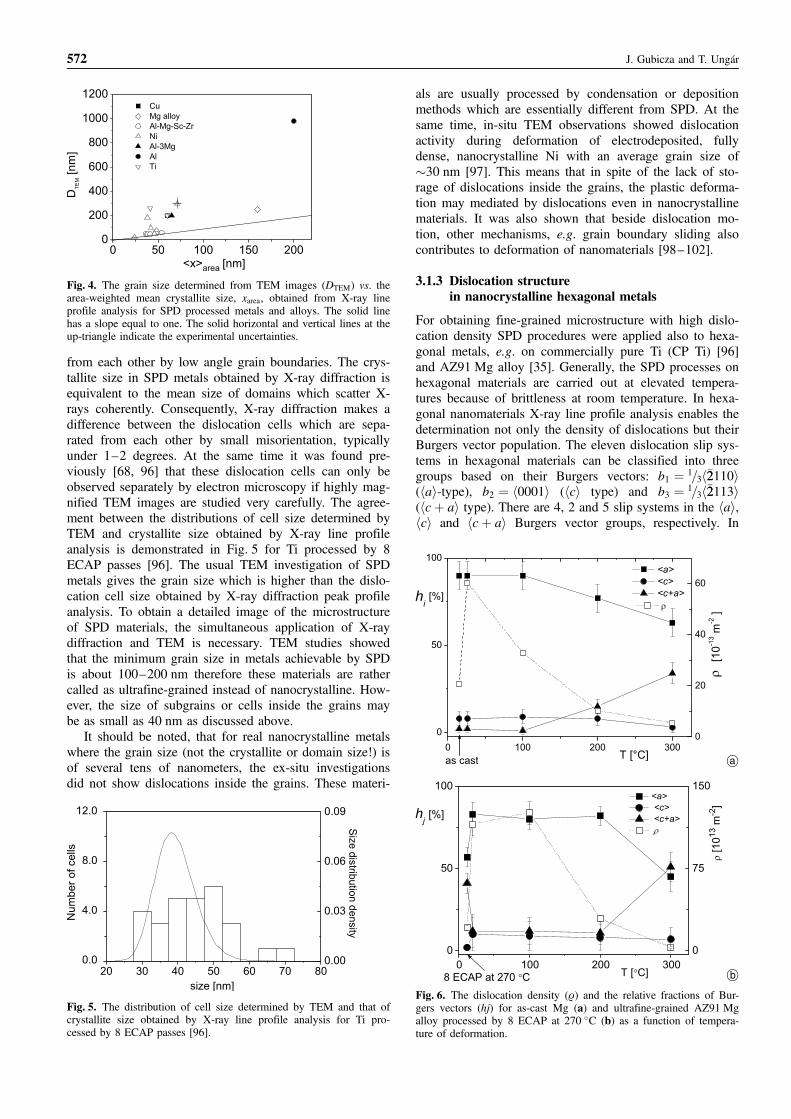
In Fig. 4 the grain size determined from TEM imagesare compared with the mean crystallite size, hxiarea, ob-tained from X-ray line profile analysis for SPD processedmetals and alloys. The mean crystallite size determined byX-rays is generally lower than the grain size observed inthe TEM images which has been already reported forother SPD materials previously [19, 68, 96]. This differ-ence may be explained by the hierarchical microstructureof SPD metals. The grains in SPD materials are dividedinto subgrains and/or dislocation cells which are separated
Defect structures by X-ray line profile analysis 571
Fig. 2. The area-weighted mean crystallite size (hxiarea), the disloca-tion density (r) and the yield strength (sY) as a function of numberof ECAP passes for Al-6082 alloy.
Fig. 3. The dislocation density (r) versus the area-weighted meancrystallite size (hxiarea) for bulk nanocrystalline and ultrafine-grainedmetals. The solid horizontal and vertical lines at the down-triangleindicate the experimental uncertainties.
Th
is a
rticle
is p
rote
cte
d b
y G
erm
an
co
pyrig
ht la
w. Y
ou
may c
op
y a
nd
dis
tribu
te th
is a
rticle
for y
ou
r pers
on
al u
se o
nly
. Oth
er u
se is
on
ly a
llow
ed
with
writte
n p
erm
issio
n b
y th
e c
op
yrig
ht h
old
er.
from each other by low angle grain boundaries. The crys-tallite size in SPD metals obtained by X-ray diffraction isequivalent to the mean size of domains which scatter X-rays coherently. Consequently, X-ray diffraction makes adifference between the dislocation cells which are sepa-rated from each other by small misorientation, typicallyunder 1–2 degrees. At the same time it was found pre-viously [68, 96] that these dislocation cells can only beobserved separately by electron microscopy if highly mag-nified TEM images are studied very carefully. The agree-ment between the distributions of cell size determined byTEM and crystallite size obtained by X-ray line profileanalysis is demonstrated in Fig. 5 for Ti processed by 8ECAP passes [96]. The usual TEM investigation of SPDmetals gives the grain size which is higher than the dislo-cation cell size obtained by X-ray diffraction peak profileanalysis. To obtain a detailed image of the microstructureof SPD materials, the simultaneous application of X-raydiffraction and TEM is necessary. TEM studies showedthat the minimum grain size in metals achievable by SPDis about 100–200 nm therefore these materials are rathercalled as ultrafine-grained instead of nanocrystalline. How-ever, the size of subgrains or cells inside the grains maybe as small as 40 nm as discussed above.
It should be noted, that for real nanocrystalline metalswhere the grain size (not the crystallite or domain size!) isof several tens of nanometers, the ex-situ investigationsdid not show dislocations inside the grains. These materi-
als are usually processed by condensation or depositionmethods which are essentially different from SPD. At thesame time, in-situ TEM observations showed dislocationactivity during deformation of electrodeposited, fullydense, nanocrystalline Ni with an average grain size of�30 nm [97]. This means that in spite of the lack of sto-rage of dislocations inside the grains, the plastic deforma-tion may mediated by dislocations even in nanocrystallinematerials. It was also shown that beside dislocation mo-tion, other mechanisms, e.g. grain boundary sliding alsocontributes to deformation of nanomaterials [98–102].
3.1.3 Dislocation structurein nanocrystalline hexagonal metals
For obtaining fine-grained microstructure with high dislo-cation density SPD procedures were applied also to hexa-gonal metals, e.g. on commercially pure Ti (CP Ti) [96]and AZ91 Mg alloy [35]. Generally, the SPD processes onhexagonal materials are carried out at elevated tempera-tures because of brittleness at room temperature. In hexa-gonal nanomaterials X-ray line profile analysis enables thedetermination not only the density of dislocations but theirBurgers vector population. The eleven dislocation slip sys-tems in hexagonal materials can be classified into threegroups based on their Burgers vectors: b1 ¼ 1=3h�22110i(hai-type), b2 ¼ h0001i (hci type) and b3 ¼ 1=3h�22113i(hcþ ai type). There are 4, 2 and 5 slip systems in the hai,hci and hcþ ai Burgers vector groups, respectively. In
572 J. Gubicza and T. Ungar
Fig. 4. The grain size determined from TEM images (DTEM) vs. thearea-weighted mean crystallite size, xarea, obtained from X-ray lineprofile analysis for SPD processed metals and alloys. The solid linehas a slope equal to one. The solid horizontal and vertical lines at theup-triangle indicate the experimental uncertainties.
Fig. 5. The distribution of cell size determined by TEM and that ofcrystallite size obtained by X-ray line profile analysis for Ti pro-cessed by 8 ECAP passes [96].
Fig. 6. The dislocation density (r) and the relative fractions of Bur-gers vectors (hj) for as-cast Mg (a) and ultrafine-grained AZ91 Mgalloy processed by 8 ECAP at 270 �C (b) as a function of tempera-ture of deformation.
a�
b�

Th
is a
rticle
is p
rote
cte
d b
y G
erm
an
co
pyrig
ht la
w. Y
ou
may c
op
y a
nd
dis
tribu
te th
is a
rticle
for y
ou
r pers
on
al u
se o
nly
. Oth
er u
se is
on
ly a
llow
ed
with
writte
n p
erm
issio
n b
y th
e c
op
yrig
ht h
old
er.
commercially pure Ti specimen processed by 8 ECAPpasses at 400–450 �C, the dislocation density obtainedfrom X-ray line profile analysis is 44 � 1014 m�2. The re-lative fractions of the hai, hci and hcþ ai Burgers vectorsare 62%, 0–4% and 32–36%, respectively. The abundanceof hai-type dislocations besides the hci- and hcþ ai-typedislocations has been also found for SPD processed Mgalloys [35]. The relatively high fraction of hcþ ai disloca-tions in hexagonal materials processed by ECAP can beattributed to the high temperature of deformation. Theoreti-cal calculations and TEM observations for hexagonal me-tallic materials suggest the activation of hcþ ai disloca-tions by strong deformation at elevated temperatures [102].At room temperature the critical resolved shear stress ofpyramidal hcþ ai dislocations is about five times largerthan that for basal slip [98], but this value decreases withincreasing temperature. The development of the dislocationdensity and the Burgers vector population as a function oftemperature of deformation are compared for coarse-grained Mg and ultrafine-grained AZ91 Mg alloy pro-cessed by high temperature ECAP in Fig. 6. The relativefraction of the hcþ ai dislocations is high even in the in-ital state obtained after ECAP-processing as it was carriedout at high temperature (270 �C). The dislocation densityis higher for any deformation temperature in the case ofultrafine-grained material because of the higher defect den-sity in the starting state processed by ECAP. The increaseof the population of hcþ ai dislocations occurs at highertemperature for the ultrafine-grained sample than for theas-cast sample. This is probably due to fact that for ultra-fine grained materials grain boundary sliding also contri-butes to the macroscopic deformation beside the sliding ofdislocations therefore the driving force to activate hcþ aidislocation is less than for coarse grained materials.
3.1.4 Planar faults in nanocrystalline metallic materials
The eCMWP procedure described above is applied toevaluate planar fault densities together with dislocationdensities and crystallite size in nanocrystalline and submi-cron grain-size copper specimens. Bulk nanocrystallinecopper specimens were prepared by inert gas condensation(IGC) and hot compaction at Argonne National Labora-tory [30, 103–106]. They are denoted as O2––IS, P2––IS,and N2––IS in the as-prepared state (initai state) and P2––Tand N2––C after tensile and compression tests, respec-tively. The notations are the same as in Weertman andSanders [104], Sanders [105], Sanders et al. [106] and Un-gar et al. [30, 103]. Submicron grain-size copper sampleswere prepared by ECAP either in the laboratory of Profes-sor Valiev [107] or in the laboratory of Professor Estrin[108] denoted as ECAP(a) or ECAP(b), respectively. Thetwin densities, b are shown as a function of the area-weighted mean crystallite size, hxiarea for the different na-nocrystalline and submicron grain size specimens inFig. 7. The values of b gives the probability of finding atwin boundary between two neighboring (111) latticeplanes. The dashed line is to guide the eye. It can be seenthat when the subgrain size is larger than about 40 nm thetwin density is close to zero, within experimental error. Atsubgrain-size values smaller than about 40 nm the twin
density increases sharply and reaches values up to 6%. Onthe basis of the model calculations and the experimentalvalues of staking fault energy in Cu, Zhu et al. [109] sug-gest 40 nm as the critical grain size below which deforma-tion proceeds by twinning instead of dislocation glide.Figure 7 shows an excellent correlation with this sugges-tion: when the area-weighted mean crystallite size is largerthan about 40 nm the twin density, within experimentalerror, is close to zero. It should be noted that this limitingvalue of crystallite size may change with the stacking faultenergy (SFE) of the metal. It has been shown [110] thatfor Cu-10 wt% Zn where the SFE is about half of that forpure Cu, the severe plastic straining of HPT results in arelatively high twin density of 4.8% even for the crystal-lite size of 50 nm. Comparing pure Cu and Cu-10 wt% Znspecimens, the lower SFE results in also a lower crystal-lite size (70 nm was determined for Cu) and 2.5 timeshigher dislocation density [110].
3.2 Ceramics
Dense nanocrystalline ceramic materials are usually pro-duced by sintering of nanopowders. The effect of the sizedistribution of the starting ceramic powders and the sinter-ing conditions (e.g. temperature and pressure) on the mi-crostructure of the compacted bulk material has been stud-ied by X-ray line profile analysis in several papers [9, 16,111]. Louer et al. [111] have determined the shape, sizeand size distribution of crystallites in nanocrystalline ZnOpowder synthesized by thermal decomposition of zinc hy-droxinitrate. Although the line breadths show a strong hkldependence, the harmonic pairs of reflections, e.g. 100–300 and 002–004 were identical within experimental er-rors. These observations were attributed to the shape ani-sotropy of the crystallites. In the quantitative evaluation ofthe Fourier transforms of the profiles, the crystallites aremodelled by cylinders. It was found that the axis of thecylinder was parallel to the hexagonal c axis and the aver-age diameter and height were 11 and 24 nm, respectively.TEM micrographs have confirmed the same shape aniso-tropy and average size values, although they showed that
Defect structures by X-ray line profile analysis 573
Fig. 7. The twin density as a function of the area-weighted meancrystallite size, hxiarea, for different nanocrystalline Cu specimens. In-ert gas condensed and compacted specimens: O2–IS, P2–IS, P2–T,N2–IS, and N2–C. Submicron grain-size samples deformed byECAP: ECAP (a) open left triangles and ECAP (b) open squares,respectively. The dashed line is to guide the eye. The solid verticalline indicates the experimental uncertainty [30, 103–108].

Th
is a
rticle
is p
rote
cte
d b
y G
erm
an
co
pyrig
ht la
w. Y
ou
may c
op
y a
nd
dis
tribu
te th
is a
rticle
for y
ou
r pers
on
al u
se o
nly
. Oth
er u
se is
on
ly a
llow
ed
with
writte
n p
erm
issio
n b
y th
e c
op
yrig
ht h
old
er.
the real shape of the crystallites is prism with irregularhexagonal cross section.
Bulk ultrafine-grained tungsten-carbide specimen wasproduced by ball-milling of submicron size powder andsubsequent sintering at high temperature (1420 �C). Thecrystallite size distribution of nanopowders obtained byball-milling and the bulk specimen produced by sinteringwere studied by X-ray line profile analysis [9]. The linebreadths decreased down to about one-third during sinter-ing as a consequence of the grain-growth at high tempera-ture consolidation. The good agreement between the crys-tallite size distribution determined by line profile analysisand TEM has been observed for the sintered tungsten-car-bide sample [9]. The good correlation between the meancrystallite size determined by X-ray diffraction, about2.4 nm, and that obtained from TEM micrographs, about3.5 nm, was also observed for a CeO2 ceramic powder[16]. This powder was prepared by decomposition ofCe2O(NO3)6 H2O in nitrogen athmosphere at 230 �C. Itwas found that the strain contribution to peak broadeningis also negligible for this material.
The crystallite size in silicon nitride ceramic powdersdetermined by X-ray line profile analysis were also com-pared with TEM observations and specific surface areameasurements [11]. A silicon nitride powder was pro-duced by nitridation of silicon and subsequent milling[11]. The area weighted mean crystallite size, hxiarea,X-ray
¼ 62(5) nm, agrees well with the area weighted mean par-ticle size calculated from the specific surface area deter-mined by the Brunauer-Emmett-Teller (BET) methodhxiarea,BET ¼ 71(5) nm. The crystallite size distribution wasalso in very good agreement with that obtained from TEMmicrographs. Another Si3N4 powder was prepared by gas-phase synthesis of silicon-tetrachloride and ammonia inthermal plasma reactor and post-crystallization at 1500 �Cfor 2 h. It was found that the mean size obtained fromline profile analysis, hxiarea,X-ray ¼ 93(5) nm was in goodagreement with that determined by BET methodhxiarea,BET ¼ 94(5) nm. It was found that the TEM particlesize distribution contained somewhat smaller particles thanthose in the crystallite size distribution obtained from lineprofile analysis. This is unusual among the comparativestudies of X-ray and TEM sizes since in general the grainsize determined by X-ray is smaller than that established
by TEM. The phenomena can be explained by the smalleramorphous grains in the powder.
Figure 8 shows the grain size determined by TEM forceramic materials discussed here versus the area-weightedmean crystallite size obtained by X-ray line profile analy-sis. It can be concluded that for nanocrystalline ceramicmaterials the two size values agree well. This means thatusually the grains or particles in the bulk or powder cera-mic materials, respectively, are single crystals, i.e. in con-trast with metals they are not divided into smaller do-mains, e.g. by dislocation cell-walls. In multiple-phaseceramic materials where the particles consists of crystal-lites of different phases, the particle size can be largerthan the crystallite as shown in the case of zirconia cera-mics [112]. In ceramic powders containing amorphousfraction the crystallite size can be smaller or higher thanthe particle size.
3.3 Diamond and silicon carbide
Bulk nanostructured diamond may be consolidated fromnanopowders under high pressure and high temperatureconditions. From the agreement between the particle sizedistributions of the starting powders obtained by line pro-file analysis and BET method, it was concluded that forthe size below 30 nm, the diamond particles are singlecrystals similarly as for ceramic powders [113]. The Wil-liamson-Hall plots show that these particles are dislocationfree but they contain significant amount of planar faults[113]. The diamond powders with the particle size higherthan 30 nm contains dislocations and their density in-creases during sintering procedure. Bulk ultrafine graineddiamond can be also processed by sintering of micron-sized powders. During consolidation at high pressure andtemperature, dislocations are formed and the grains aredivided into subgrains or dislocation cells, similarly as inmetals by severe plastic deformation [113]. The disloca-tion formation is induced by the contact shear stresses ex-erted by the edges of neighboring particles in the com-pressed powder.
Silicon carbide is also frequently used as a functionaland structural material at high temperatures. Nanocrystal-line SiC offers very high strength either as a bindingphase in diamond composites or as a single phase materialeven at high temperatures [114]. Ultrafine grained bulkSiC samples are usually fabricated from nanopowders bysintering at high pressures and temperatures. It is expectedthat the microstructure of sintered SiC can be tailored bythe proper selection of these two parameters [114].
To study the effect of the sintering conditions on themicrostructure, bulk nanocrystalline SiC specimens weresintered from SiC nanopowder with nominal grain size of30 nm. The sintering procedure was carried out at tem-peratures of 1400, 1600 and 1800 �C. At each tempera-ture, specimens were sintered at pressures of 2, 4 and5.5 GPa. This process gave nine bulk sintered SiC sam-ples, in addition to the initial powder. An additional speci-men was produced at 1800 �C and at a very high sinteringpressure of 8 GPa. The lattice defect structure and thecrystallite size are studied by X-ray line profile analysisand transmission electron microscopy. For revealing the
574 J. Gubicza and T. Ungar
Fig. 8. The grain size determined from TEM images (DTEM) vs. thearea-weighted mean crystallite size, xarea, obtained from X-ray lineprofile analysis for nanostructured ceramic materials. The solid linehas a slope equal to one. The size of the symbols represents the un-certainty of data.
Th
is a
rticle
is p
rote
cte
d b
y G
erm
an
co
pyrig
ht la
w. Y
ou
may c
op
y a
nd
dis
tribu
te th
is a
rticle
for y
ou
r pers
on
al u
se o
nly
. Oth
er u
se is
on
ly a
llow
ed
with
writte
n p
erm
issio
n b
y th
e c
op
yrig
ht h
old
er.
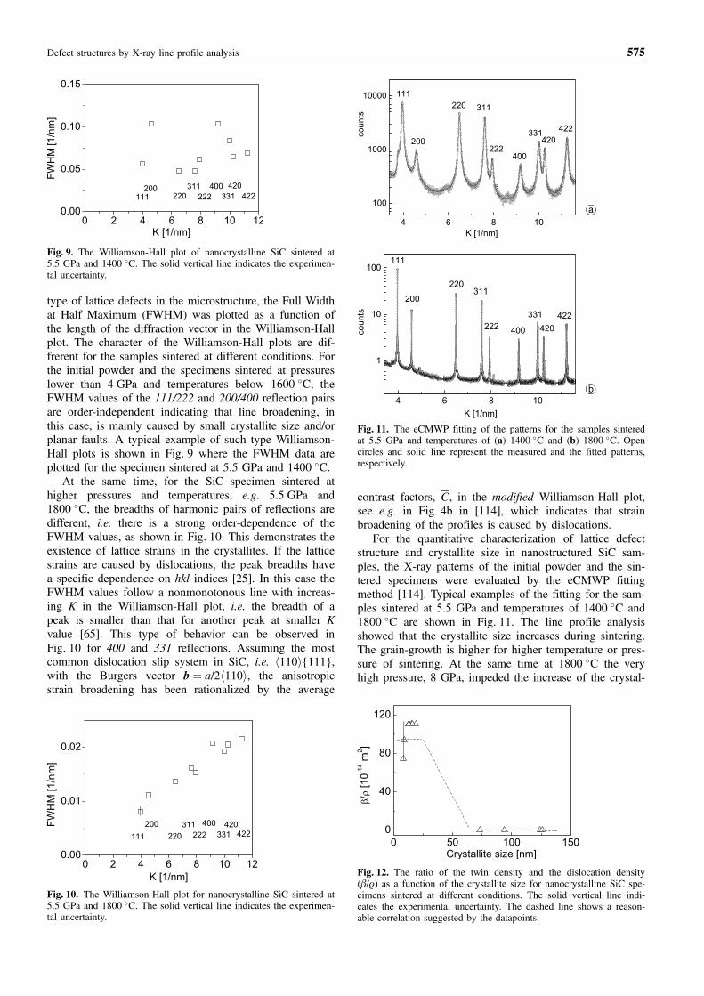
type of lattice defects in the microstructure, the Full Widthat Half Maximum (FWHM) was plotted as a function ofthe length of the diffraction vector in the Williamson-Hallplot. The character of the Williamson-Hall plots are dif-frerent for the samples sintered at different conditions. Forthe initial powder and the specimens sintered at pressureslower than 4 GPa and temperatures below 1600 �C, theFWHM values of the 111/222 and 200/400 reflection pairsare order-independent indicating that line broadening, inthis case, is mainly caused by small crystallite size and/orplanar faults. A typical example of such type Williamson-Hall plots is shown in Fig. 9 where the FWHM data areplotted for the specimen sintered at 5.5 GPa and 1400 �C.
At the same time, for the SiC specimen sintered athigher pressures and temperatures, e.g. 5.5 GPa and1800 �C, the breadths of harmonic pairs of reflections aredifferent, i.e. there is a strong order-dependence of theFWHM values, as shown in Fig. 10. This demonstrates theexistence of lattice strains in the crystallites. If the latticestrains are caused by dislocations, the peak breadths havea specific dependence on hkl indices [25]. In this case theFWHM values follow a nonmonotonous line with increas-ing K in the Williamson-Hall plot, i.e. the breadth of apeak is smaller than that for another peak at smaller Kvalue [65]. This type of behavior can be observed inFig. 10 for 400 and 331 reflections. Assuming the mostcommon dislocation slip system in SiC, i.e. h110i{111},with the Burgers vector b ¼ a/2h110i, the anisotropicstrain broadening has been rationalized by the average
contrast factors, C, in the modified Williamson-Hall plot,see e.g. in Fig. 4b in [114], which indicates that strainbroadening of the profiles is caused by dislocations.
For the quantitative characterization of lattice defectstructure and crystallite size in nanostructured SiC sam-ples, the X-ray patterns of the initial powder and the sin-tered specimens were evaluated by the eCMWP fittingmethod [114]. Typical examples of the fitting for the sam-ples sintered at 5.5 GPa and temperatures of 1400 �C and1800 �C are shown in Fig. 11. The line profile analysisshowed that the crystallite size increases during sintering.The grain-growth is higher for higher temperature or pres-sure of sintering. At the same time at 1800 �C the veryhigh pressure, 8 GPa, impeded the increase of the crystal-
Defect structures by X-ray line profile analysis 575
Fig. 9. The Williamson-Hall plot of nanocrystalline SiC sintered at5.5 GPa and 1400 �C. The solid vertical line indicates the experimen-tal uncertainty.
Fig. 10. The Williamson-Hall plot for nanocrystalline SiC sintered at5.5 GPa and 1800 �C. The solid vertical line indicates the experimen-tal uncertainty.
Fig. 11. The eCMWP fitting of the patterns for the samples sinteredat 5.5 GPa and temperatures of (a) 1400 �C and (b) 1800 �C. Opencircles and solid line represent the measured and the fitted patterns,respectively.
a�
b�
Fig. 12. The ratio of the twin density and the dislocation density(b/r) as a function of the crystallite size for nanocrystalline SiC spe-cimens sintered at different conditions. The solid vertical line indi-cates the experimental uncertainty. The dashed line shows a reason-able correlation suggested by the datapoints.

Th
is a
rticle
is p
rote
cte
d b
y G
erm
an
co
pyrig
ht la
w. Y
ou
may c
op
y a
nd
dis
tribu
te th
is a
rticle
for y
ou
r pers
on
al u
se o
nly
. Oth
er u
se is
on
ly a
llow
ed
with
writte
n p
erm
issio
n b
y th
e c
op
yrig
ht h
old
er.
lite size. Examination of the TEM images confirmed thatconclusion. A correlation between the crystallite size andthe lattice defect structure has been established. Figure 12shows the ratio of the twin density and the dislocationdensity (b/r) as a function of the crystallite size for nano-crystalline SiC specimens sintered at different conditions.It can be concluded that the increase of the crystallite sizeis accompanied by the reduction of planar fault probabilityand by the increase of the dislocation density. This resultis also in line with previous observations for Cu andCu––Zn alloys discussed above in this paper. The criticalvalue of crystallite size for nc-SiC, where dislocations areabundant instead of planar faults, is estimated to be be-tween 25 and 70 nm.
3.4 Polymers
The effect of plastic deformation on the lattice defect struc-ture in nanostructured monoclinic a-phase isotactic poly-propylene (PP) was studied by X-ray line profile analysis[115]. The specimens were plastically deformed by rollingto different strain values up to 49.6%. For the coherentlyscattering domain size, or “apparent crystallite size”, theevaluation yields a continuous decrease with increasingplastic deformation. The resulting domain sizes lie between20 nm for the undeformed and 15 nm for the deformedspecimen, where etrue ¼ 50%. This value is in good correla-tion with the lamella thickness of polypropylene [115]. TheWilliamson-Hall plot in Fig. 13 shows a strong order de-pendence of peak breadths. Using the average dislocationcontrast factors, C, the FWHM values can be arrangedalong a smooth curve in the modified Williamson-Hallplot, as it can be seen in Fig. 14. This means that the latticedefects in melt-crystallised and plastically deformed poly-propylene have the same type of strain field as for disloca-tions, therefore we can call these defects as dislocations.
The modified Williamson-Hall plot was used only forthe examination of the source of lattice strain in the micro-structure. The dislocation density was evaluated by profilefitting method (CMWP). It was found that the dislocationdensity increases with deformation, as it can be seen inFig. 15. The dislocation densities of plastically deformed
PP are between 1016 and 1017 m�2. The reported disloca-tion densities in polypropylene are considerably higherthan the values for common metals. An explanation is thelong-chain nature of the macromolecules which cause ad-ditional constraints when polymer crystals develop. This,in some natural way, leads to the strong production of dis-locations already in the undeformed materials [116]. Thehigher initial dislocation density might yields higher num-ber of sources for dislocation generation during deforma-tion compared to metallic materials.
4. Summary
The fundamentals of the method of X-ray line profile ana-lysis is discussed in terms of: (i) strain anisotropy, and thedislocation model of strain anisotropy, (ii) the qualitativeinformation provided by the different breadth methods,especially the Williamson-Hall and modified Williamson-Hall plots and the modified Warren-Averbach procedure,(iii) the more sophisticated and more quantitative methodsof whole profile and whole pattern fitting procedures. Theefficiency of the procedure is demonstrated by discussingthe defect structures in metals, ceramics, diamond and SiCnanocrystals and polymers. It is shown that, especially in
576 J. Gubicza and T. Ungar
Fig. 13. Classical Williamson-Hall plot for polypropylene peaks(1 1 0), (0 4 0), (1 3 0), (0 5 0) and (0 4 1) deformed by rolling upto etrue ¼ 49.6%. The solid vertical line indicates the experimentaluncertainty.
Fig. 14. Modified Williamson-Hall plot for the same sample andpeaks as in Fig. 13. The solid vertical line indicates the experimentaluncertainty.
Fig. 15. Dislocation density versus the true strain for the rolled poly-propylene specimens. The solid vertical line indicates the experimen-tal uncertainty.

Th
is a
rticle
is p
rote
cte
d b
y G
erm
an
co
pyrig
ht la
w. Y
ou
may c
op
y a
nd
dis
tribu
te th
is a
rticle
for y
ou
r pers
on
al u
se o
nly
. Oth
er u
se is
on
ly a
llow
ed
with
writte
n p
erm
issio
n b
y th
e c
op
yrig
ht h
old
er.
bulk metallic submicron grain size and nanomaterials pro-cessed by plastic deformation, the X-ray crystallite size isin best correlation with the subgrain size or dislocationcell size provided by TEM or HRTEM. In the case of pow-der or sintered bulk ceramics X-ray crystallite size is ingood agreement with TEM particle or grain size, respec-tively. It has been shown that twinning and faulting canreadily be determined together with the dislocation struc-ture and size properties. It was found that in submicrongrain size and nanocrystalline copper twinning becomessubstantial when the crystallite size is smaller than about40 nm. In nanocrystalline SiC, starting from a twinnednano-powder, twinning has been enhanced when crystallitesize remained small during sintering, whereas, grain coar-sening caused by sintering is accompanied by increaseddislocation activity at the cost of twinning. In polypropy-lene X-ray line profile analysis has provided extremelylarge dislocation densities in good correlation with thesmall lamella thickness in this structure.
Acknowledgments. The authors are grateful for the financial supportof the Hungarian National Science Foundation, OTKA T46990,T67692 and F47057. This work was supported by the Bolyai JanosResearch Scholarship of the Hungarian Academy of Sciences.
References
[1] Warren, B. E.: X-ray Studies of Deformed Metals. Progr. MetalPhys. 8 (1959) 147–202.
[2] Wilson, A. J. C.: X-Ray Optics, the Diffraction of X-Rays byFinite and Imperfect Crystals. London, Methuen, 1962.
[3] Delhez, R.; de Keijser, Th. H.; Mittemeijer, E. J.: Determinationof crystallite size and lattice-distortions through X-ray-diffrac-tion line-profile analysis – Recipes, methods and comments.Fresnius Z Anlz. Chem. 312 (1982) 1–16.
[4] Louer, D.; Auffredic, J. P.; Langford, J. I.; Ciosmak, D.; Niepce,J. C.: A precise determination of the shape, size and distributionof size of crystallites in zinc oxide by X-ray line-broadeninganalysis. J. Appl. Cryst. 16 (1983) 183–191.
[5] Langford J. I.; Louer, D.: High-resolution powder diffractionstudies of copper(II) oxide. J. Appl. Cryst. 24 (1991) 149–155.
[6] Langford, J. I.; Boultif, A.; Auffredic, J. P.; Louer, D.: The useof pattern decomposition to study the combined X-ray diffrac-tion effects of crystallite size and stacking faults in ex-oxalatezinc oxide. J. Appl. Cryst. 26 (1993) 22–33.
[7] Balzar, D.; Ledbetter, H.: Voigt-function modeling in Fourieranalysis of size- and strain-broadened X-ray diffraction peaks. J.Appl. Cryst. 26 (1993) 97.
[8] Krill, C. E.; Birringer, R.: Estimating Grain-Size Distributions inNanocrystalline Materials form X-Ray Diffraction Profile Analy-sis. Phil. Mag. 77 (1998) 621–640.
[9] Ungar, T.; Borbely, A.; Goren-Muginstein, G. R.; Berger S.; Ro-sen, A. R.: Particle-size, size distribution and dislocations in na-nocrystalline tungsten-carbide. Nanostructured Materials 11(1999) 103–113.
[10] Langford, J. I.; Louer D.; Scardi, P.: Effect of a crystallite sizedistribution on X-ray diffraction line profiles and whole-powder-pattern fitting. J. Appl. Cryst. 33 (2000) 964–974.
[11] Gubicza, J.; Szepvolgyi, J.; Mohai, I.; Zsoldos L.; Ungar, T.:Particle size distribution and the dislocation density determinedby high resolution X-ray diffraction in nanocrystalline siliconnitride powders. Mat. Sci. Eng. A280 (2000) 263–269.
[12] Scardi, P.; Leoni, M.: Diffraction line profiles from polydispersecrystalline systems. Ata Cryst. A57 (2001) 604–613.
[13] Szepvolgyi, J.; Mohai, I.; Gubicza, J.: Atmospheric ageing of nano-sized silicon nitride powders. J. Mater. Chem. 11 (2001) 859–863.
[14] Rafaja, D.; Klemm, V.; Schreiber, G.; Knapp, M.; Kuzel, R.:Interference phenomena observed by X-ray diffraction in nano-crystalline thin films. J. Appl. Cryst. 37 (2004) 613–620.
[15] Leoni, M.; Scardi, P.: Nanocrystalline domain size distributionsfrom powder diffraction data. J. Appl. Cryst. 37 (2004) 629–634.
[16] Balzar, D.; Audebrand, N.; Daymond, M. R.; Fitch, A.; Hewat,A.; Langford, J. I.; Le Bail, A.; Louer, D.; Masson, O.; McCo-wan, C. N.; Popa, N. C.; Stephens, P. W.; Toby, B. H.: Size-strain line-broadening analysis of the ceria round-robin sample.J. Appl. Cryst. 37 (2004) 911–924.
[17] Pielaszek, R.: FW1/5/4/5M method for determination of thegrain size distibution form powder diffraction line profile. J. Al-loys Comp. 382 (2004) 128–132.
[18] Shen, T. D.; Schwarz, R. B.; Thompson, J. D.: Soft magnetismin mechanically alloyed nanocrystalline materials. Pys. Rev. B72(2005) 014431.
[19] Ungar, T.; Tichy, G.; Gubicza J.; Hellmig, R. J.: Correlationbetween subgrains and coherently-scattering-domains. PowderDiffr. 20 (2005) 366–375.
[20] Rafaja, D.; Poklad, A.; Klemm, V.; Schreiber, G.; Heger, D.;Sıma, M.; Dopita, M.: Some consequences of the partial crystal-lographic coherence between nanocrystalline domains inTi––Al––N and Ti––Al––Si––N coatings. Thin Solid Films 514(2006) 240–249.
[21] Krivoglaz, M. A.: X-ray and Neutron Diffraction in NonidealCrystals, Springer-Verlag. Berlin. Heidelberg. New York, 1996.
[22] Wilkens, M.: Determination of density and distribution of dislo-cations in deformed single crystals from broadened X-ray dif-fraction profiles. phys. stat. sol. (a) 2 (1970) 359–370.
[23] Wilkens, M.: Fundamental Aspects of Dislocation Theory (Eds.J. A. Simmons, R. de Wit, R. Bullough) p. 1195. Nat. Bur.Stand. Spec. Publ. Vol. II. No. 317. Washington DC. USA,1970.
[24] Wilkens, M.: Proc. 8th Int. Conf. Strength Met. Alloys (ICSMA8). Tampere. Finland. (Eds. P. O. Kettunen, T. K. Lepisto, M. E.Lehtonen) p. 47. Pergamon Press, 1988.
[25] Ungar, T.; Borbely, A.: The effect of dislocation contrast on X-ray line broadening: a new approach to line profile analysis.Appl. Phys. Lett. 69 (1996) 3173–3175.
[26] Groma, I.; Ungar T.; Wilkens, M. J.: Asymmetric X-ray-linebroadening of plastically deformed crystals.1. Theory. Appl.Cryst. 21 (1988) 47–53.
[27] Groma, I.: X-ray line broadening due to an inhomogeneous dis-location distribution. Phys. Rev. B57 (1998) 7535–7542.
[28] Kuzel Jr., R.; Klimanek, P.: X-ray diffraction line broadeningdue to dislocations in non-cubic materials. 2. The case of elas-tic-anisotropy applied to hexagonal crystals. J. Appl. Cryst. 21(1988) 363–368.
[29] Kuzel Jr., R.; Klimanek, P.: X-ray diffraction line broadeningdue to dislocations in non-cubic materials. 3. Experimental re-sults for plastically deformed zirconium. J. Appl. Cryst. 22(1989) 299–307.
[30] Ungar, T.; Ott, S.; Sanders, P.; Borbely, A.; Weertman, J. R.: Dis-locations, grain size and planar faults in nanostructured copperdetermined by high resolution X-ray diffraction and a new proce-dure of peak profile analysis. Acta mater. 46 (1998) 3693–3699.
[31] Ungar, T.; Tichy, G.: The effect of dislocation contrast on X-rayline profiles in untextured polycrystals. phys. stat. sol. (a) 147(1999) 425–434.
[32] Ungar, T.; Leoni, M.; Scardi, P.: The dislocation model of strainanisotropy in whole powder-pattern fitting: the case of anLi––Mn cubic spinel. J. Appl. Cryst. 32 (1999) 290–295.
[33] Mathis, K.; Nyilas, K.; Axt, A.; Cernatescu, I. D.; Ungar, T.;Lukac, P.: The evolution of non-basal dislocations as a functionof deformation temperature in pure magnesium determined byX-ray diffraction. Acta Mater. 52 (2004) 2889–2894.
[34] Cordier, P.; Ungar, T.; Zsoldos, L.; Tichy, G.: Dislocation creepin MgSiO3 perovskite at conditions of the Earth’s uppermostlower mantle. Nature 428 (2004) 837–840.
[35] Mathis, K.; Gubicza, J.; Nam, N. H.: Microstructure and me-chanical behavior of AZ91 Mg-alloy processed by Equal Chan-nel Angular Pressing. J. Alloys Comp. 394 (2005) 194–199.
[36] Ungar, T.; Castelnau, O.; Ribarik, G.; Drakopoulos, M.; Be-chade, J. L.; Chauveau, T.; Snigirev, A.; Snigireva, I.; Schroer,C.; Bacroix, B.: Grain to grain slip activity in plastically de-formed Zr determined by X-ray micro-diffraction line profileanalysis. Acta Materialia 55 (2007) 1117–1127.
Defect structures by X-ray line profile analysis 577

Th
is a
rticle
is p
rote
cte
d b
y G
erm
an
co
pyrig
ht la
w. Y
ou
may c
op
y a
nd
dis
tribu
te th
is a
rticle
for y
ou
r pers
on
al u
se o
nly
. Oth
er u
se is
on
ly a
llow
ed
with
writte
n p
erm
issio
n b
y th
e c
op
yrig
ht h
old
er.
[37] Hendricks, S. B.; Jefferson, M. E.; Schultz, J. F.: XXII. The transi-tion temperatures of cobalt and of nickel, some observations onthe oxides of nickel. Z. Kristallogr. 73 (1930) 376–380.
[38] Landau, L.: The scattering of X-rays by crystals with variablelamellar structure. Phys. Z. SowjUn. 12 (1937) 579–585.
[39] Lifschitz, M.: On the theory of scattering of X-rays by crystalsof variable structure. Phys. Z. SowjUn. 12 (1937) 623–643.
[40] Hendricks, S.; Teller, E.: X-ray interference in partially orderedlayer lattices. J. Chem. Phys. 10 (1942) 147–167.
[41] Jagodzinski, H.: Eindimensionale Fehlordnung in Kristallen undihr Einfluss auf die Rontgeninterferenzen. II. Berechnung derfehlgeordneten dichtesten Kugelpackungen mit Wechselwirkun-gen der Reichweite 3. Acta Cryst. 2 (1949) 208–214.
[42] Treacy, M. M. J.; Newsam, J. M.; Deem, M. W.: A general re-cursion method for calculating diffracted intensities from crys-tals containing planar faults. Proc. Roy. Soc. London A433(1991) 499–520.
[43] Ustinov, A. I.: Defect and Microstructure Analysis by Diffrac-tion (Eds. R. L. Snyder, J. Fiala, and H. J. Bunge) pp. 264–317.Oxford University Press. 1999.
[44] Ustinov, A. I.; Olikhovska, L. O.; Budarina, N. M.; Bernard, F.:Diffraction analysis of the microstructure of materials (Eds. E. J.Mittemeijer, P. Scardi) p. 309. Springer-Verlag. Berlin, Heidel-berg. 2004.
[45] Scardi, P.; Leoni, M.: Fourier modelling of the anisotropic linebroadening of X-ray diffraction profiles due to line and planelattice defects. J. Appl. Cryst. 32 (1999) 671–682.
[46] Estevez-Rams, E.; Penton-Madrigal, A.; Lora-Serrano, R.; Marti-nez-Garcia, J.: Direct determination of microstructural para-meters from the X-ray diffraction profile of a crystal with stack-ing faults. J. Appl. Cryst. 34 (2001) 730–736.
[47] Estevez-Rams, E.; Lora-Serrano, R.; Penton-Madrigal, A.;Fuess, H.: Quantitative analysis of planar faulting. Acta Cryst.A58 (Supplement) (2002) C233.
[48] Estevez-Rams, E.; Leoni, M.; Scardi, P.; Aragon-Fernandez, B.;Fuess, H.: On the powder diffraction pattern of crystals withstacking faults. Philosophical Magazine. 83 (2003) 4045–4057.
[49] Leoni, M.; Gualtieri, A. F.; Roveri, N.: Simultaneous refinementof structure and microstructure of layered materials. J. Appl.Cryst. 37 (2004) 166–173.
[50] Kuznetsov, A.; Dmitriev, V.; Langenhorst, F.; Estevez-Rams, E.;Dubrovinskay, L.: Stacking Faults and Internal Strains in DHCPPhase of La. Acta Cryst. A61 (2005) C451
[51] Balogh, L.; Ribarik G.; Ungar, T.: Stacking Faults and TwinBoundaries in fcc Crystals Determined by X-ray Diffraction Pro-file Analysis. J. Appl. Phys. 100 (2006) 023512.
[52] Ungar, T.; Mughrabi, H.; Ronnpagel D.; Wilkens, M.: X-rayline-broadening study of the dislocation cell structure in de-formed [001]-orientated coper single crystals. Acta Met. 32(1984) 333–342.
[53] Mughrabi, H.; Ungar, T.; Kienle W.; Wilkens, M.: Long rangeinternal stresses and asymmetric X-ray line broadening in ten-sile-deformed [001]-orientated coper single crystals. Phil. Mag.A53 (1986) 793–813.
[54] Noyan, I. C.; Cohen, J. B.: Residual stress: measurement by dif-fraction and interpretation. Spinger-Verlag. New York. 1987.
[55] Lahrman, D.; Field, R.; Darolia R.; Fraser, H.: Investigation oftechniques for measuring lattice mismatch in a rhenium contain-ing nickel base superalloy. Acta metall. 36 (1988) 1309–1320.
[56] Kuhn, H. A.; Biermann, H.; Ungar, T.; Mughrabi, H.: X-raystudy of creep-deformation induced changes of the lattice mis-match in the g0-hardened monocrystalline nickel-base superalloySRR 99. Acta Met. Mater. 39 (1991) 2783–2794.
[57] Mughrabi, H.; Biermann, H.; Ungar, T.: Creep-induced local lat-tice parameter changes in a monocrystalline Nickel-base super-alloy. Journal of Materials Engineering and Performance 2(1993) 557–564.
[58] Ungar, T.; Biermann, H.; von Grossmann, B.: Synchrotron mi-crobeam diffraction study of the microstructure and the chemicalcomposition in a monocrystalline Ni-base turbine blade after athermo mechanical mission test. Structural Chemistry 14 (2003)49–56.
[59] Leineweber, A.; Mittemeijer, E. J.: Anisotropic microstrainbroadening due to compositional inhomogeneities and its para-metrisation. Z. Kristallogr. Suppl. 23 (2006) 117–122, Part 1.
[60] Wilson, A. J. C.; Zsoldos, L.: The Reflexion of X-Rays from the‘Anti-Phase Nuclei’ of AuCu3. II. Proc Roy Soc London A290(1966) 508–514.
[61] Scardi, P.; Leoni, M.: Diffraction whole-pattern modelling studyof anti-phase domains in Cu3Au. Acta Materialia 53 (2005)5229–5239.
[62] Schafler, E.; Steiner, G.; Korznikova, E.; Kerber M.; Zehetbauer,M. J.: Lattice defect investigation of ECAP-Cu by means of X-ray line profile analysis, calorimetry and electrical resistometry.Mater. Sci. Eng. A410–411 (2005) 169–173.
[63] Cervellino, A.; Giannini, C.; Guagliardi, A.; Ladisa, M.: Nano-particle size distribution estimation by a full-pattern powder dif-fraction analysis Phys. Rev. B72 (2005) 035412.
[64] Ribarik, G.; Audebrand, N.; Palancher, H.; Ungar, T.; Louer, D.:Dislocations and crystallite size distributions in ball-milled nano-crystalline fluorides MF2 (M ¼ Ca, Sr, Ba, Cd) determined byX-ray diffraction-line-profile analysis, J. Appl. Cryst. 38 (2005)912–926.
[65] Palosz, B.; Stelmakh, S.; Grzanka, E.; Gierlotka, S.; Palosz, W.:Application of the apparent lattice parameter to determination ofthe core-shell structure of nanocrystals. Z. Kristallogr. 222(2007) 580–594.
[66] Ungar, T.; Gubicza, J.: Nanocrystalline Materials Studied byPowder Diffraction Line Profile Analysis. Z. Kristallogr. 222(2007) 114–128.
[67] Bertaut, E. F.: Raies de Debye-Scherrer et repartition des dimen-sions des domaines de Bragg dans les poudres polycristallines.Acta Cryst. 3 (1950) 14–18.
[68] Ungar, T.; Gubicza, J.; Ribarik, G.; Borbely, A.: Crystallitesize distribution and dislocation structure determined by dif-fraction profile analysis: Principles and practical application tocubic and hexagonal crystals. J. Appl. Cryst. 34 (2001) 298–310.
[69] Guinier, A.: X-ray Diffraction. Freeman, San Francisco, (1963).[70] Leoni, M.; Scardi, P.: Nanocrystalline domain size distributions
from powder diffraction data. J. Appl. Cryst. 37 (2004) 629–634.[71] Langford, J. I.; Boultif, A.; Auffredic, J. P.; Louer, D.: The use
of pattern decomposition to study the combined X-ray diffrac-tion effects of crystallite size and stacking-faults in ex-oxalatezinc-oxide. J. Appl. Cryst. 26 (1993) 22–33.
[72] Louer, D.; Auffredic, J. P.; Langford, J. I.; Ciosmak D.; Niepce,J. C.: A precise determination of the shape, size and distributionof size crystallites in zinc-oxide by X-ray line broadening analy-sis. J. Appl. Cryst. 16 (1983) 183–191.
[73] Williamson, G. K.; Hall, W. H.: X-ray Line Broadening fromFiled Al and W. Acta metall. 1 (1953) 22–31.
[74] Stokes, A. R.; Wilson, A. J. C.: A method of calculating theintegral breadths of Debye-Scherrer lines. Proc. Camb. Phil.Soc. 38 (1942) 313–322.
[75] Kuzel Jr., R.; Klimanek, P.: X-ray diffraction line broadeningdue to dislocations in non-cubic materials. 2. The case of elas-tic-anisotropy applied to hexagonal crystals. J. Appl. Cryst. 21(1988) 363–368.
[76] Kuzel Jr., R.; Klimanek, P.: X-ray diffraction line broadeningdue to dislocations in non-cubic materials. 3. Experimental re-sults for plastically deformed zirconium. J. Appl. Cryst. 22(1989) 299–307.
[77] Ungar, T.; Borbely, A.: The effect of dislocation contrast on X-ray line broadening: a new approach to line profile analysis.Appl. Phys. Lett. 69 (1996) 3173–3175.
[78] Revesz, A.; Ungar, T.; Borbely A.; Lendvai, J.: Dislocations andgrain size in ball-milled iron powder. Nanostr. Mater. 7 (1996)779–788.
[79] Hinds, W. C.: Aerosol Technology: Properties, Behavior andMeasurement of Airbone Particles, New York: Wiley, 1982.
[80] Scardi, P.; Leoni, M.; Delhez, R.: Line broadening analysisusing integral breadth methods: a critical review. J. Appl. Cryst.37 (2004) 381–390.
[81] Ungar, T.; Gubicza, J.; Tichy, G.; Pantea C.; Zerda, T. W.: Sizeand shape of crystallites and internal stresses in carbon blacks.Composites Part A: Applied Science and manufacturing 36(2005) 431–436.
[82] Pantea, C.; Gubicza, J.; Ungar, T.; Voronin, G.; Zerda, T. W.:Dislocation density and graphitization of diamond crystals.Phys. Rev. B66 (2002) art. no. 094106.
578 J. Gubicza and T. Ungar

Th
is a
rticle
is p
rote
cte
d b
y G
erm
an
co
pyrig
ht la
w. Y
ou
may c
op
y a
nd
dis
tribu
te th
is a
rticle
for y
ou
r pers
on
al u
se o
nly
. Oth
er u
se is
on
ly a
llow
ed
with
writte
n p
erm
issio
n b
y th
e c
op
yrig
ht h
old
er.
[83] Scardi, P.; Dong, Y.; Leoni, M.: Line profile analysis in Riet-veld method and Whole Powder Pattern Fitting. Mater. Sci.Forum 378–381 (2001) 132–139.
[84] Ribarik, G.; Ungar, T.; Gubicza, J.: MWP-fit: A program formultiple whole-profile fitting of diffraction peak profiles by abinitio theoretical functions. J. Appl. Cryst. 34 (2001) 669–676.
[85] Scardi, P.; Leoni, M.: Whole powder pattern modelling. ActaCryst. A58 (2002) 190–200.
[86] Velterop, L.; Delhez, R.; deKeijser, T. H.; Mittemeijer E. J.;Reefman, D.: X-ray diffraction analysis of stacking and twinfaults in F.C.C metals: a revision and allowance for texture andnon-uniform fault probabilities. J. Appl. Crystallogr. 33 (2000)296–306.
[87] Dragomir, I. C.; Ungar, T.: Contrast factors of dislocations inthe hexagonal crystal system. J. Appl. Cryst. 35 (2002) 556–564.
[88] Ungar, T.; Glavicic, M. G.; Balogh, L.; Nyilas, K.; Salem,A. A.; Ribarik G.; Semiatin, S. L.: Mater. Sci. Eng. A, sub-mitted.
[89] Balogh, L.; Ribarik, G.; Ungar, T.: in preparation.[90] Ungar, T.: Micro structural parameters from X-ray diffraction
peak broadening. Scripta Mater. 51 (2004) 777–781.[91] Zhilyaev, A. P.; Gubicza, J.; Nurislamova, G.; Revesz, A.; Suri-
nach, S.; Baro, M. D.; Ungar, T.: Microstructural Characteriza-tion of Ultrafine-Grained Nickel. phys. stat. sol. (a) 198 (2003)263–271.
[92] Chinh, N. Q.; Gubicza, J.; Langdon, T. G.: Face-centered cubicmetals and alloys processed by Equal-Channel Angular Press-ing. J. Mater. Sci. 42 (2007) 1594–1605.
[93] Gubicza, J.; Chinh, N. Q.; Krallics, Gy.; Schiller, I.; Ungar, T.:Microstructure of ultrafine-grained fcc metals produced by se-vere plastic deformation. Curr. Appl. Phys. 6 (2006) 194–199.
[94] Valiev, R. Z.; Islamgaliev, R. K.; Alexandrov, I. V.: Bulk nano-structured materials from severe plastic deformation. Progr.Mater. Sci. 45 (2000) 103–189.
[95] Gubicza, J.; Chinh, N. Q.; Horita, Z.; Langdon, T. G.: Effectof Mg addition on microstructure and mechanical properties ofaluminum. Mater. Sci. Eng. A387–389 (2004) 55–59.
[96] Zhu, Y. T.; Huang, J. Y.; Gubicza, J.; Ungar, T.; Wang, Y. M.;Ma, E.; Valiev, R. Z.: Nanostructures in Ti Processed by SeverePlastic Deformation. J. Mat. Res. 18 (2003) 1908–1917.
[97] Kumar, K. S.; Suresh, S.; Chisholm, M. F.; Horton, J. A.;Wang, P.: Deformation of electrodeposited nanocrystalline nick-el. Acta Materialia 51 (2003) 387–405
[98] Swygenhoven, H.; Farkas, D.; Caro, A.: Grain-boundary struc-tures in polycrystalline metals at the nanoscale. Phys. Rev. B62(2000) 831–838.
[99] Swygenhoven, S. H.; Derlet, P. M.; Hasnaoui, A.: AtomisticModeling of Strength of Nanocrystalline Metals. Advanced En-gineering Materials 5 (2003) 345–350.
[100] Schiøtz, J.; DiTolla, F. D.; Jacobsen, K. W.: Softening of nano-crystalline metals at very small grain sizes. Nature 391 (1998)561–563.
[101] Schiøtz, J.; Vegge, T.; DiTolla, F. D.; Jacobsen, K. W.: Atomic-scale simulations of the mechanical deformation of nanocrystal-line metals. Phys. Rev. B60 (1999) 11971–11983.
[102] Yoo, M. H.: Slip, twinning and fracture in hexagonal close-packed metals. Metall. Trans. A12 (1981) 409–418.
[103] Ungar, T.; Tichy, G.; Sanders, P. G.; Weertman, J. R.: Disloca-tions in Submicron Grain Size and Nanocrystalline Copper.Mater. Res. Soc. Symp. Proc. 634 (2001) B1.7.1–6.
[104] Weertman, J. R.; Sanders, P. G.: Plastic Deformation of Nano-crystalline Metals. Solid State Phenomena 35–36 (1994) 249–262.
[105] Sanders, P. G.: Ph.D. thesis. Northwestern University, 1996.[106] Sanders, P. G.; Fougere, G. E.; Thompson, L. J.; Eastman,
J. A.; Weertman, J. R.: Improvements in the synthesis and com-paction of nanocrystalline materials. Nanostruct. Mater. 8(1997) 243–252.
[107] Valiev, R. Z.; Kozlov, E. V.; Ivanov, Yu.; F. Lian, J.; Nazarov,A. A.; Baudelet, B.: Deformation behavior of ultra-fine-grainedcopper. Acta Metall. Mater. 42 (1994) 2467–2475.
[108] Baik, S. C.; Estrin, Y.; Kim, H. S.; Jeong, H. T.; Hellmig, R. J.:Calculation of deformation behavior and texture evolution dur-ing equal channel angular pressing of IF steel using dislocationbased modeling of strain hardening. Mater. Sci. Forum 408–412 (2002) 697–702.
[109] Zhu, Y. T.; Liao, X. Z.; Srinivasan, S. G.; Lavernia, E. J.: Nu-cleation of deformation twins in nanocrystalline face-centered-cubic metals processed by severe plastic deformation. J. Appl.Phys. 98 (2005) 034319.
[110] Zhao, Y. H.; Zhu, Y. T.; Liao, X. Z.; Horita, Z.; Langdon,T. G.: Tailoring stacking fault energy for high ductility andhigh strength in ultrafine grained Cu and its alloy. Appl. Phys.Lett. 89 (2006) 121906.
[111] Louer, D.; Auffredic, J. P.; Langford, J. I.; Ciosmak, D.;Niepce, J. C.: Thermodynamic study of the thermal decomposi-tion of zinc hydroxinitrates. J. Appl. Cryst. 183 (1983) 16–23.
[112] Lin, J. D.; Duh, J. G.: The use of X-ray line profile analysis inthe tetragonal to monoclinic phase transformation of ballmilled, as-sintered and thermally aged zirconia powders. J.Mat. Sci. 32 (1997) 4901–4908.
[113] Palosz, B.; Grzanka, E.; Pantea, C.; Zerda, T. W Wang.; Gubic-za, J.; Ungar, T.: Microstructure of nanocrystalline diamondpowders studied by powder diffractometry. J. Appl. Phys. 97(2005) 064316.
[114] Gubicza, J.; Nauyoks, S.; Balogh, L.; Zerda, T. W.; Ungar, T.:Influence of sintering temperature and pressure on crystallitesize and lattice defect structure in nanocrystalline SiC. J. Ma-ter. Res. 22 (2007) 1314–1321.
[115] Wilhelm, H.; Paris, A.; Schafler, E.; Bernstorff, S.; Bonarski,J.; Ungar, T.; Zehetbauer, M. J.: Evidence of dislocations inmelt-crystallised and plastically deformed polypropylene. Mate-rials Science and Engineering A387–389 (2004) 1018–1022.
[116] Lin, L.; Argon, A. S.: Structure and plastic deformation ofpolyethylene. J. Mater. Sci. 29 (1994) 294–323.
Defect structures by X-ray line profile analysis 579