Performance Characterization & Call Reliability Diagnosis Support ...

Invited Paper
Characterization and reliability of CMOS microstructuresGary K. Fedder* and R. D. (Shawn) Blantona
aDepament of Electrical and Computer Engineering and bThe Robotics Institute
Carnegie Mellon University, Pittsburgh, PA 15213-3890, USA
ABSTRACTThis paper provides an overview of high-aspect-ratio CMOS micromachining, focusing on materials characterization,reliability, and fault analysis. Composite microstructural beam widths and gaps down to 1 .2 tm are etched out of conventionalCMOS dielectric, aluminum, and gate-polysilicon thin films using post-CMOS dry etching for both structural sidewalldefinition and for release from the substrate. Differences in stress between the multiple metal and dielectric layers causevertical stress gradients and curl, while misalignment between layers causes lateral stress gradients and curl. Cracking isinduced in a resonant fatigue structure at 620 MPa of repetitive stress after over 50millioncycles. Beams have withstood over1 .3 billion cycles at 124 MPa stress levels induced by electrostatic actuation. Failures due to process defects are classifiedaccording to the geometrical features of the defective structures. Relative probability of occurrence of each defect type isextracted from the process simulation results.
Keywords: CMOS-MEMS, characterization, reliability, defect analysis
1. INTRODUCTION
CMOS micromachining is a way of making integrated MEMS that was first invented ten years ago1. Since that time, several
kinds of CMOS MEMS processing have been developed to meet a variety of application needs, including inertial sensors2'3,
biological cell force sensors4, thermally operated gas flow sensors5, electrothermal power converters6, and infrared detectors7.Microstructures having a single mechanical layer are made from combinations of oxide, aluminum, and polysilicon thin filmsthat are already present in conventional CMOS process flows. The metallization and dielectric layers serve a dual function aselectrical interconnect and structural material. The gate polysilicon is often used in thermal heater resistors, piezoresistive
sensors, and thermopiles8. Since conventional CMOS is inexpensive technology, perfecting CMOS micromachining will leadto commercial integrated CMOS-MEMS that are readily accessible from multiple vendors at low cost.
A common CMOS micromachining process uses stacked vias in the CMOS followed by a wet silicon undercut etch to createstructures. These kinds of structures are available through some foundries, provided that end users perform the silicon etch forrelease. Some European foundries support a full CMOS micromachining process flow. Another way to make CMOSmicrostructures, which is being explored at Carnegie Mellon, is to perform the structural etch after the CMOS iscompleted9'10. Post-CMOS etching allows independent development of the MEMS process steps. Well-defined sidewalls canbe formed with nearly vertical slope, and beam and gap widths can be pushed to less than 2 tim. The ability to make narrowgaps enables design of lateral electrostatic actuation and lateral capacitive detection at performance levels rivaling surface-micromachined polysilicon technology. Likewise, the ability to make narrow beams enables design of lateral suspensions thatare not realizable in earlier CMOS MEMS processes. However, CMOS micromachining is relatively immature compared topolysilicon MEMS and much research is necessary to fully characterize and understand the failure mechanisms. Initial effortsin characterizing mechanical properties and in understanding reliability issues of the CMOS MEMS process is the focus of this
paper.
*Correspondence: Email: [email protected]; WWW:http://www.ece.cmu.edul—mems; Tel: (412) 268-4594; Fax: (412) 268-4595
Part of the SPIE Conference on MEMS Reliability for Critical and Space Applications1 Santa Clara, California • September 1999
SPIE Vol. 3880 . 0277-786X199/$1 0.00
Downloaded From: http://proceedings.spiedigitallibrary.org/ on 11/08/2015 Terms of Use: http://spiedigitallibrary.org/ss/TermsOfUse.aspx
© 1999 IEEE. Personal use of this material is permitted. Permission from IEEE must be obtained for all other uses, in any current or future media, including reprinting/republishing this material for advertising or promotional purposes, creating new collective works, for resale or redistribution to servers or lists, or reuse of any copyrighted component of this work in other works.

dielectricmetal-3metal-2
(a) metal-ipolysiliconsilicon substrate
(b) -
(c) ?TF E __Figure i . Cross sections of the high-aspect-ratio CMOS micromachining process flow.
(a) After CMOS processing.(b) After directional reactive-ion etch of dielectric for definition of structural sidewalls.
(c) After isotropic plasma etch of silicon for structural release.(d) The end of a fabricated m3-m2-mi-poly beam.
2. FABRICATION PROCESS
Microstructures are defined after completion of the CMOS processing by two reactive-ion etching (RIE) steps, as illustrated inFigure 1. First, a CHF3/02 anisotropic etch of the dielectric layers defines the structural sidewalls resulting in the cross sectionin Figure 1(b). The top metal layer in the CMOS process flow is used as an etch-resistant mask for the microstructuredefinition. Next, a nearly isotropic SF6/02 etch undercuts the silicon substrate and releases the structure as shown inFigure 1(c). The scanning electron micrograph in Figure 1(d) is of a released composite beam with three metal conductors andpolysilicon. Fourteen different composite structures can be made by using different combinations of the embedded metallayers and polysilicon. In Figure 1(a)-(c), three kinds of beams are depicted. By omitting the upper metal layers, beams havinga variety of thicknesses can be fabricated.
We have made MEMS structures in several processes including Hewlett-Packard 0.8 im three-metal CMOS, Hewlett-Packard0.5 jtm three-metal CMOS, Hewlett-Packard 0.35 jtm four-metal CMOS, and the TSMC 0.35tm four-metal CMOS. Figure 2demonstrates the ability to transfer the post-CMOS micromachining steps to various kinds of CMOS. A simple 'crab-leg'resonator is shown fabricated in each of three different processes. The two 0.35 .tm processes require chem-mechanicalpolishing for planarization of interconnect, which puts restrictions on the size open metal areas. The waffle shaped pieces ofmaterial left in the etch pits are remnants of metal fill that were automatically placed in the layout. In subsequent runs, thedesigner can place metal fill areas that are mechanically anchored to avoid this situation.
Factorial experiments were performed to optimize the microstructural etching recipes11. Electrical connection failures at viasconnecting different metal layers can result from lengthy etch times and from use of improper etch recipes. Failures are causedby two mechanisms as shown in Figure 3: one is milling of the metal exposed at the top the vias which results in an opencircuit at the sidewall; the second is lateral etching of refractory metal layers which exist above and below each aluminumlayer in most sub-micron CMOS processes. Some passivation of the sidewalls during the structural etch step is necessary toprevent the attack of the refractory metal layers during the SF6 release Si etch.
Devices made in our CMOS-MEMS process include accelerometers12, vibratory-rate gyroscopes13, and microactuators forprobe-based data storage14. The lateral capacitive accelerometer in Figure 4 has a measured sensitivity of i .2 mVIgIV andnoise floor of 0.5 mg/rtHz. A perforated plate of CMOS dielectric and metal layers acts as the proof mass and is suspended bysprings attached to each of its four corners. Electrical connections to the capacitive sense fingers are routed through thesprings. The fingers are arranged in a fully differential common-centroid configuration to improve sensitivity and reduceeffects of manufacturing variations.
133
Downloaded From: http://proceedings.spiedigitallibrary.org/ on 11/08/2015 Terms of Use: http://spiedigitallibrary.org/ss/TermsOfUse.aspx

-t)l (
Jr1b;r-Lrfl;
e1415 ZKY
- —— —"fflr.-51 TTTI((}-
34
Figure 2. Crab-leg microresonators fabricated in three separate CMOS processes.(a) HP 0.5 rim, (b) HP 0.35 tm, (c) TSMC 0.35 .tm
Figure 3. Via failure mechanism11. (a) Loss of critical dimension by ion milling,(b) Lateral etch of refractory layer illustrated by FIB cross-cut of structure.
_ U
11.*..- —I.::::::::::::::: RUIU::::::::::::::::
'U::::
U'U'
::::::::::::.:::::::: I,II• UI•
40()
Figure 4. A lateral capacitive accelerometer made by micromachining the dielectric layers in the HE 0.5 1m process.(a) Top view of the device. (b) Schematic showing the capacitive displacement sensing with common centroid, fully
differential design.
''r
C
C:J jre—
C.
Downloaded From: http://proceedings.spiedigitallibrary.org/ on 11/08/2015 Terms of Use: http://spiedigitallibrary.org/ss/TermsOfUse.aspx
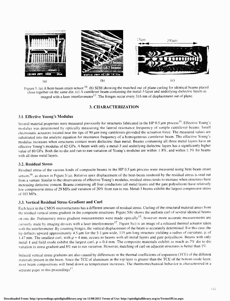
Figure 5. (a) A bent-beam strain sensor 16 (b) SEM showing the matched out-of-plane curling for identical beams placedclose together on the same die. (c) A cantilever beam containing the metal-3 layer and underlying dielectric layers as
imaged with a laser interferometer17. The fringes occur every 316 nm of displacement out of plane.
3. CHARACTERIZATION
3.1. Effective Young's Modulus
Several material properties were measured previously for structures fabricated in the HP 0.5.tm processt5. Effective Young'smodulus was determined by optically measuring the lateral resonance frequency of simple cantilever beams. Smallelectrostatic actuators located near the tips of 90 im-long cantilevers provided the actuation force. The measured values aresubstituted into the analytic equation for resonance frequency of a homogeneous cantilever beam. The effective Young'smodulus increases when structures contain more dielectric than metal. Beams containing all three metal layers have aneffective Young's modulus of 62 GPa. A beam with only a metal-3 and underlying dielectric layers has a significantly highervalue of 80 GPa. Both die-to-die and run-to-run variation of Young's modulus are within 8%, and within 3% for beamswith all three metal layers.
3.2. Residual StressResidual stress of the various kinds of composite beams in the HP 0.5 im process were measured using bent-beam strainsensors16, as shown in Figure 5 (a). Relative apex displacement of the bent-beam rendered by the residual stress is read outfrom a vernier. Similar to the observations of effective Young's modulus, residual stress tends to increase when structures haveincreasing dielectric content. Beams containing all four conductors (all metal layers and the gate polysilicon) have relativelylow compressive stress of 29 MPa and variation of 20% from run to run. Metal-3 beams exhibit the largest compressive stressof 103 MPa.
3.3. Vertical Residual Stress Gradient and CurlEach layer in the CMOS microstructures has a different amount of residual stress. Curling of the structural material arises fromthe residual vertical stress gradient in the composite structures. Figure 5(b) shows the uniform curl of several identical beams
on one die. Preliminary stress gradient measurements were made optically'5. however more accurate measurements arecurrently made by imaging devices with a laser interferometert7. Figure 5(c) is an image of a released thermal actuator takens ith the interferometer. By counting fringes, the vertical displacement of the beam is accurately determined. For this case, thetip deflects upward approximately 4.5 .tm for the 5.1 ).tm-wide. 115 .tm-long structure yielding a radius of curvature. p. of1.47 mm. The smallest curl, with p =4mm, occurs in beams with all metal layers and gate polysilicon. Beams with onlymetal-I and field oxide exhibit the largest curl, p =0.4 mm. The composite materials exhibit as much as 7% die to dievariation in stress gradient and 8% run to run variation. However, matching of curl on adjacent structures is better than 1%.
Induced vertical stress gradients are also caused by differences in the thermal coefficients of expansion (iCE) of the differentmaterials present in the beam. Since the TCE of aluminum in the top layer is greater than the TCE of the bottom oxide layer.most beam compositions will bend down as temperature increases. The thermomechanical behavior is characterized in a
separate paper in this proceedings'7.
(a) (b) (c)
Downloaded From: http://proceedings.spiedigitallibrary.org/ on 11/08/2015 Terms of Use: http://spiedigitallibrary.org/ss/TermsOfUse.aspx

(a) .:
beamswith 'lateralbending
Figure 6. (a) Arrays of cantilevers showing lateral bending of narrow beams. (b) A cantilever beam test structure fabricatedusing the HP 0.35 tm process. Schematics of the beam cross sections are indicated. Lateral curl due to inner layer
misalignment is evident. Cantilever resonators are visible in the background.
3.4. Lateral Residual Stress Gradient and CurlLateral curling is an effect unique to high-aspect-ratio CMOS processing caused by manufacturing misalignment of the innerfilm layers in very narrow beams. Lateral curl is visible in the cantilever array shown in Figure 6(a) for beams having a narrowwidth of less than 3 .tm. An example of a test structure to measure lateral curl is shown in Figure 6(b). The left, center andright beams have corresponding layout with inner metal layers purposely shifted left, centered and shifted right, respectively.The lateral curl in each beam results from a lateral stress gradient formed by the asymmetry of the beam cross-section. A largeamount of vertical curl is also evident. Lateral curl can be relieved by improved lithography alignment, however wafer runoutprohibits complete elimination of this effect. It is possible to change sensitivity of lateral curl to misalignment by modifyingthe layout of inner metal layers, so the future possibility exists to reduce the value and variation of lateral curl.
An example of how lateral curl affects performance of devices was uncovered during testing of the CMOS accelerometershown in Figure 4. A mechanical offset of the proof mass of around 0.4 j.tm was present due to lateral curling of the 1.5 j.tm-wide suspension beams. The fabricated air gap in the parallel-plate capacitive sensor when the proof mass is perfectly centeredis 2.0 tm. The offset, which is 20% of the gap, was compensated by applying a dc voltage to self-test actuators to pull the massinto a centered position. Reducing the number of spring meanders and widening the beams in the suspension will reduce theoffset, but the resultant decrease in accelerometer sensitivity is undesirable. Widening of capacitance sense fingers to reducelateral curl improves the manufacturability of the device.
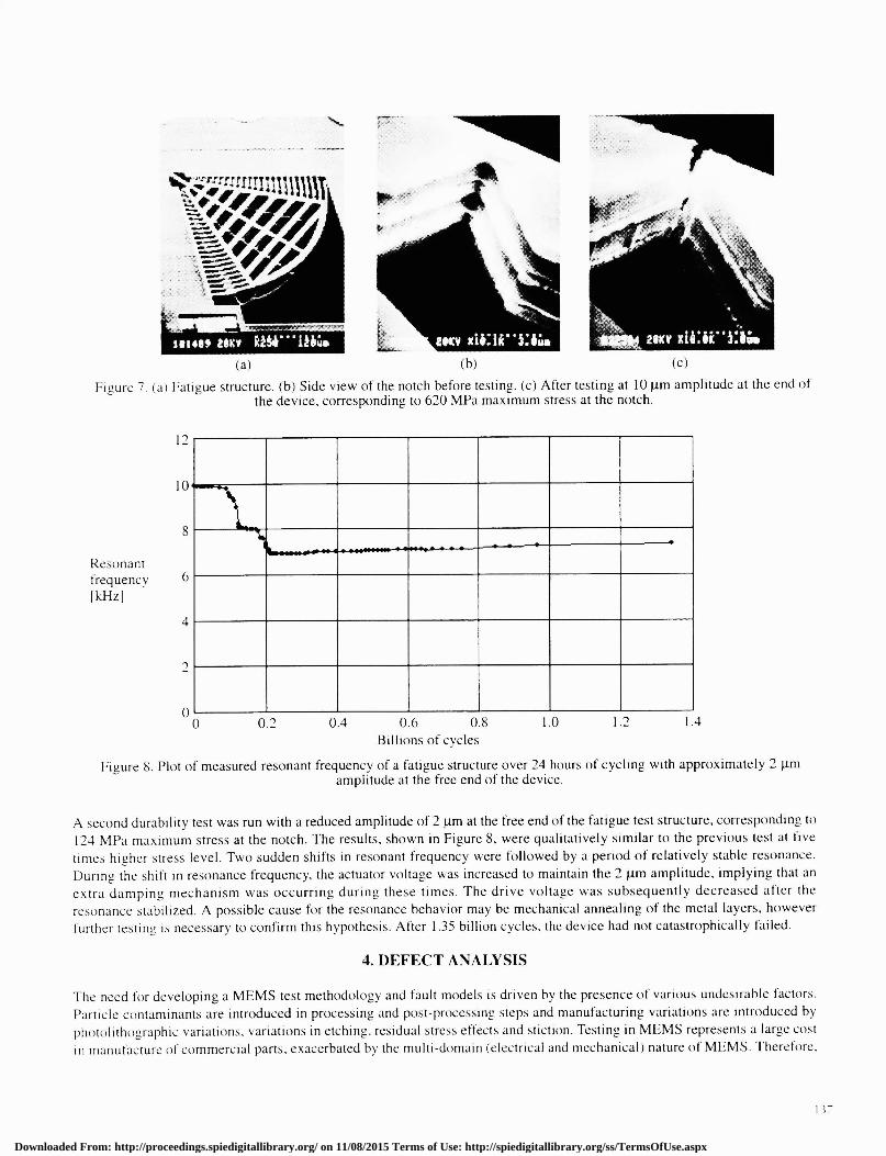
3.5. Cyclic FatigueCyclic fatigue of CMOS microstructures was investigated by using a modified test structure obtained from Failure Analysis
Associates, Inc.18, as shown in Figure 7(a). The device is a large wedge-shaped plate mass that is suspended at its base by abeam with a lateral notch designed into its side. Comb-finger electrostatic actuators are placed to drive the plate in an angulardirection. Sufficient stress concentration induced by cyclic motion near the notch gives rise to crack growth and causes failureof the structure.
In our prior work, we ran a durability test by cyclically stressing the notch to 620 MPa, which is about 1% of the effectivemodulus of elasticity of the composite beam15. This value of stress corresponds to a displacement amplitude of 10 .tm at thefree end of the structure, as determined through finite-element analysis. The lowest resonance is an out-of-plane mode excitedfrom pull-down forces generated by the upward curling comb-finger electrodes. This lowest mode is avoided by driving thedevice at the resonant frequency of the lateral mode. At resonance, the drive requires 40 V ac. in series with a d.c. bias of55 V. Resonance frequency of the structure was initially 13. 1 kHz. During the test the resonance frequency decreased by 10%and stabilized after approximately 10 million cycles. The notch snapped off after 72 minutes and over 45millioncycles, and isshown before and after failure in Figure 7 (b) and (c).
136
Downloaded From: http://proceedings.spiedigitallibrary.org/ on 11/08/2015 Terms of Use: http://spiedigitallibrary.org/ss/TermsOfUse.aspx
Billions of cycles
Figure 8. Plot of measured resonant frequency of a fatigue structure over 24 hours of cycling with approximately 2 jimamplitude at the free end of the device.
A second durability test was run with a reduced amplitude of 2 tm at the free end of the fatigue test structure, corresponding to124 MPa maximum stress at the notch. The results, shown in Figure 8, were qualitatively similar to the ViOUS test at livetimes higher stress level. Two sudden shifts in resonant frequency were followed by a period ot relatively stable resonance.During the shift in resonance frequency, the actuator voltage was increased to maintain the 2 jim amplitude, implying that anextra damping mechanism was occurring during these times. The drive voltage was subsequently decreased after theresonance stabilized. A possible cause for the resonance behavior may he mechanical annealing of the metal layers, howeverfurther testing is necessary to confirm this hypothesis. After 1.35 billion cycles, the device had not catastrophically failed.
4. DEFECT ANALYSIS
The need for developing a MEMS test methodology and fault models is driven by the presence of various undesirable factors.Particle contaminants are introduced in processing and post-processing steps and manufacturing variations are introduced byphotolithographic variations, variations in etching. residual stress effects and stiction. Testing in MEMS represents a large costin manufacture of commercial parts. exacerbated b the multi-domain (electrical and mechanical) nature of MEMS. Therefore.
12
Figure 7. (a) Fatigue structure. (b) Side view of the notch before testing. (c) After testing at 10 p.m amplitude at the end ofthe device, corresponding to 620 MPa maximum stress at the notch.
Res on ant
frequency1kHz]
l:\ -..— 4.—
4
00 0.2 0.4 0.6 0.8 1.0 1.2 1.4
Downloaded From: http://proceedings.spiedigitallibrary.org/ on 11/08/2015 Terms of Use: http://spiedigitallibrary.org/ss/TermsOfUse.aspx

a robust test methodology for MEMS is needed.
Previously, we have developed a contaminant and process simulator for analyzing the misbehaviors caused by particulatecontamination in the fabrication process, called CARAMEL19. Monte Carlo use of CARAMEL has produced the fullspectrum of defective structures caused by particle contaminants. These results are used to perform defect classificationaccording to the geometrical features of the defective structures. The identified defect types fall into three categories: surface,anchor and broken structure, each of which can be further divided into a number of sub-defect categories dependent upon the
exact particle and/or defective structure location20. Figure 9 shows representative examples of these defect classes for anelectrostatic comb-finger microresonator. The particular results are for polysilicon MEMS, however they can be readilyextended to CMOS micromachining or to other MEMS processes.
The relative probability of occurrence (RPO) of each defect type was extracted from the process simulation results andcompared with theoretical calculations. RPO is a probability that estimates the likelihood of a particular defect type given thepresence of a single contamination. We also have classified all the process steps involved with manufacturing themicroresonator as either resistant or vulnerable to the particle contaminants. Mechanical and electrical analysis wereperformed to evaluate the misbehaviors of the defective structures. In mechanical simulation, we applied an inertial force, andmeasured the displacement of the microresonator under this force. In electrical simulation, we measured the output sensingvoltage from the differential capacitive-sensing model formed by the microresonator. Our results show that defects resultingfrom particles cause a range of misbehaviors. Based on the amount of deviation from the nominal, we have categorized defectsas either catastrophic (deviation > 30%), parametric (5% � deviation � 30%) and harmless (deviation <5%) based ondisplacement and sensing voltage. An important result discovered is that some defect types, such as those that affect fingergap, have virtually no impact on displacement, but dramatically affect sensing voltage.
5. CONCLUSIONS
Initial characterization studies of the CMOS MEMS process demonstrate the capability to fabricate microstructures inconventional CMOS with mechanical properties that are repeatable to within 10%. Values of residual stress and stressgradients must be well characterized in order to predict behavior of designed devices. Lateral stress gradients in CMOSmicrostructures present a unique challenge in design, and in many cases may limit the usable beam width. Further work isnecessary to understand the lateral bending fully and devise ways to reduce its effect. Cyclic stress down to at least 124 MPacauses the resonance frequency and damping of durability test structures to change with time. The physical mechanisms forthese changes are not well understood and call for future work.
Defects arising in the manufacturing process can cause yield and reliability problems. Categorizing defects in terms of theirconsequences on device operation will help drive issues in design for manufacturability for MEMS.
ACKNOWLEDGEMENTS
This research effort is sponsored by DARPA and U.S. AFRL, under agreement number F30602-97-2-0323. The authors wouldlike to thank their graduate students Steve Eagle, Tao Jiang, Hasnain Lakdawala, Michael S.-C. Lu, and Xu Zhu.
138
(c)
Figure9. Representative examples of the defect categories caused by particles: (a) Surface protrusion located on theshuttle. (b) Surface finger protrusion that welds two adjacent fingers. (c) Lateral finger protrusion that reduces
finger gap in the overlap region.
Downloaded From: http://proceedings.spiedigitallibrary.org/ on 11/08/2015 Terms of Use: http://spiedigitallibrary.org/ss/TermsOfUse.aspx

REFERENCES
1. M. Parameswaran, H.P. Baltes, L. Ristic, A. C. Dhaded and A. M. Robinson, "A new approach for the fabrication ofmicromechanical structures," Sensors and Actuators A, 19, pp. 289-307, 1989.
2. H. Seidel, U. Fritsch, R. Gottinger, J. Schalk, J. Walter and K. Ambaum, "A piezoresistive silicon accelerometer withmonolithically integrated CMOS-circuitry," in Tech. Digest, 8th mt. Conf Solid-State Sensors and Actuators (Trans-ducers '95)/Eurosensors IX, Stockholm, Sweden, Vol. 1, pp. 597-600 (1995).
3. M. Biebi, T. Scheiter, C. Hierold, H. V. Philipsborn and H. Klose, "Micromechanics compatible with an 0.8 pm CMOSprocess," Sensors andActuators A, 46-47, pp. 593-597 (1995).
4. Lin, G., Pister, K. S. J., and Roos, K. P., "Standard CMOS piezoresistive sensor to quantify heart cell contractileforces," in Proc. IEEE Micro Electro Mech. Sys. Workshop (MEMS '96), San Diego, CA, 150- 155, 1996.
5. Mayer, F., Paul, 0., and Baltes, H., "Influence of design geometry and packaging on the response of thermal CMOSflow sensors," in Tech. Digest 8th mt. Conf on Solid-State Sensors and Actuators (Transducers '95), Stockholm, Swe-den, 1, 528-531, 1995.
6. Reay, R. J., Klaasen, H., and Kovacs, G. T. A., "Thermally and electrically isolated single crystal silicon structures inCMOS technology," IEEE Electron Device Letters, 15(10) 399-401, 1994.
7. Syrzycki, M. J., Carr, L., Chapman, U. H., and Parameswaran, M., "A wafer scale visual-to-thermal converter," IEEETrans. Compon. Hybrids Manuf Technol., 16(7) 665-673, 1993.
8. H. Baltes, 0. Paul, and 0. Brand, "Micromachined Thermally Based CMOS Microsensors," Proc. ofthe IEEE, vol. 86,no. 8, Aug. 1998, pp. 1660-1678.
9. G. K. Fedder, S. Santhanam, M.L. Reed, S.C. Eagle, D.F. Guillou, M.S.-C. Lu, and L.R. Carley "Laminated High-Aspect-Ratio Microstructures in a Conventional CMOS Process", Sensors and Actuators A, 57, pp 103-1 10 1996.
10. L. R. Carley, ML. Reed, G.K. Fedder, and S. Santhanam, "Micromechanical Structure and Process of Making Same," U.S. Patent5,717,631, Feb. 10, 1998.
1 1 . X. Zhu, D. W. Greve., R. Lawton, N. Presser, and G. K. Fedder, "Factorial Experiment on CMOS-MEMS RIE Post Pro-cessing," in Proc. of the 194th Electrochemical Society Meeting, Symposium on Microstructures and MicrofabricatedSystems I% vol. 98-14, Boston, MA, Nov. 1-6, 1998, pp. 33-42.
12. G. Zhang, H. Xie, L. E. De Rosset and G. K. Fedder, "A Lateral Capacitive CMOS Accelerometer with Structural CurlCompensation," in Proc. of1EEE MEMS Conf, Orlando, FL, Jan. 17-21, 1999.
13. M. S. Kranz and G. K. Fedder, "Micromechanical Vibratory Rate Gyroscopes Fabricated in Conventional CMOS," inProceedings ofthe Symposium Gyro Technology, Stuttgart, Germany, Sept. 16-17, 1997, pp. 3.0-3.8.
14. G. K. Fedder, "Integrated MEMS in Conventional CMOS," in Tribology Issues and Opportunities in MEMS, B. Bhus-han, ed., Kluwer Academic Publishers (1998), pp.17-29.
15. M. S-C. Lu, X. Zhu, and G. K. Fedder, "Mechanical Property Measurement of 0.5 p.m CMOS Microstructures," inProc. MRS 1998 Spring Meeting, Symposium N, San Francisco, CA, April 13-17, 1998.
16. Y. B. Gianchandani and K. Najafi, 'Bent-beam strain sensors," IEEE J. ofMicroElectroMech. Sys., 5, pp. 52-58, 1996.17. S. Eagle, H. Lakdawala and G.K. Fedder, "Design and simulation of thermal actuators for STM applications in a stan-
dard CMOS process," to be published in Proceedings ofthe SPIE, Sept. 1999.18. S. B. Brown and E. Janson, in Technical Digest ofthe IEEE/LEOS 1996 Summer Topical Meetings, Optical MEMS and
their applications, pp. 9-10.19. A. Kolpekwar, T. Jiang, and R.D. Blanton, "CARAMEL: Contamination and Reliability Analysis of Microelectrome-
chanical Systems," to appear in IEEE Journal of Microelectromechanical Systems, Sept. 1999.20. T. Jiang, C. Kellen, R. D. (Shawn) Blanton, "Inductive Fault Analysis of a Microresonator," in Proceedings of Modeling
and Simulation of Microsystems '99, Puerto Rico, April 19-2 1, 1999.
139
Downloaded From: http://proceedings.spiedigitallibrary.org/ on 11/08/2015 Terms of Use: http://spiedigitallibrary.org/ss/TermsOfUse.aspx