Characteristics of Sn8Zn3Bi solder joints and crack …mme.uwaterloo.ca/~camj/pdf/Zhou/MR-2008...
7
Characteristics of Sn8Zn3Bi solder joints and crack resistance with various PCB and lead coatings Young Woo Lee a , Ki Ju Lee a , Y. Norman Zhou b , Jae Pil Jung a, * a Department of Materials Science and Engineering, University of Seoul, Seoul 130-743, Republic of Korea b Department of Mechanical Engineering, University of Waterloo, Waterloo, Canada N2L 3G1 Received 26 May 2007; received in revised form 1 September 2007 Available online 11 December 2007 Abstract Reliability of QFP (quad flat package) solder joints after thermal shock was investigated for PCB’s and connecting leads plated with several different alloy coatings before soldering. Sn–8 wt%Zn–3 wt%Bi (hereafter, Sn–8Zn–3Bi) was selected as a solder, and FR-4 PCB’s finished with Cu/Sn, Cu/OSP and Cu/Ni/Au were used as substrates. The leads of the QFP were Cu plated with Sn–10 wt%Pb, or Sn, or Sn–3 wt%Bi. The QFP chips were mounted on the substrates using a Sn–8Zn–3Bi solder paste and reflowed in air atmosphere. The pull strength and microstructure for the soldered leads of QFP were evaluated before and after thermal shock testing. The leads plated with Sn or Sn–3Bi showed approximately 40–50% higher pull strength than the reference value of a Sn–37%Pb solder joint for all PCB-fin- ishes. However, in the case of leads coated with Sn–10Pb, the pull strength of the leads soldered to a Sn-finished PCB was 21% lower than the reference value. In microstructure analysis of the joints with Sn–10Pb-plated leads, cracks were found along the bonded interface for Sn-finished PCB. The cracks were believed to start from the low melting temperature phase, 49.38 wt% Pb–32.58 wt%Sn–18.03 wt%Bi, found around the crack, and then propagated through Cu–Zn intermetallic compound. Meanwhile, even when using Sn–10Pb-plated leads, the PCB’s finished with Cu/Ni/Au coating had about 30% higher strength than the reference value, and cracks were hardly found on the soldered joint. Thus, even with Sn–10Pb-plated leads the Cu/Ni/Au-finished PCB’s were evaluated to be as reliable as the refer- ence joint. Ó 2007 Elsevier Ltd. All rights reserved. 1. Introduction In the electronic industry, Pb-bearing solders are restricted in use because of environmental concerns. Numerous Pb-free solders have been investigated to replace conventional Pb-bearing solders, and Sn–Ag–Cu, Sn–Ag– Bi, Sn–Zn–Bi and Sn–Cu based alloys are popular candi- dates [1]. Especially Sn–Ag–Cu alloy is a leading candidate [2] because of its high reliability and solderability. How- ever, high melting point and high cost are drawbacks of this solder. Meanwhile, Sn–8Zn–3Bi solder has several advantages such as a melting point (around 197 °C) that is much closer to Sn–37%Pb, good mechanical properties and low price. Considering the mechanical properties of Sn–Zn based alloys, Iwanishi et al. [3] reported that thermal shock resis- tance of soldered joints between 40 and 125 °C was better than that of Sn–37Pb. In the case of the quad flat package (QFP), the bond strength of a Sn–Zn alloy after aging at 125 °C for 2000 h, where its leads were plated with Sn–Bi before soldering, was equal to or higher than that of Sn– 37Pb [4]. During a thermal shock test, the acicular shaped Zn phase is known to be changed to a round shape although this change has not been found to cause drastic strength decrease [5]. Furthermore, study of solderability of various combina- tions of platings on electronic parts and on PCB pads is important for practical application of Sn–8Zn–3Bi solder. A study has been reported of the aging properties of Sn– 8Zn–3Bi solder joints with various lead plating but with a single plated finish coating on the PCB pads [6]. In this 0026-2714/$ - see front matter Ó 2007 Elsevier Ltd. All rights reserved. doi:10.1016/j.microrel.2007.10.005 * Corresponding author. Tel.: +82 2 2210 2981; fax: +82 2 2215 5863. E-mail address: [email protected] (J.P. Jung). www.elsevier.com/locate/microrel Available online at www.sciencedirect.com Microelectronics Reliability 48 (2008) 631–637
Transcript of Characteristics of Sn8Zn3Bi solder joints and crack …mme.uwaterloo.ca/~camj/pdf/Zhou/MR-2008...

Available online at www.sciencedirect.com
www.elsevier.com/locate/microrel
Microelectronics Reliability 48 (2008) 631–637
Characteristics of Sn8Zn3Bi solder joints and crack resistancewith various PCB and lead coatings
Young Woo Lee a, Ki Ju Lee a, Y. Norman Zhou b, Jae Pil Jung a,*
a Department of Materials Science and Engineering, University of Seoul, Seoul 130-743, Republic of Koreab Department of Mechanical Engineering, University of Waterloo, Waterloo, Canada N2L 3G1
Received 26 May 2007; received in revised form 1 September 2007Available online 11 December 2007
Abstract
Reliability of QFP (quad flat package) solder joints after thermal shock was investigated for PCB’s and connecting leads plated withseveral different alloy coatings before soldering. Sn–8 wt%Zn–3 wt%Bi (hereafter, Sn–8Zn–3Bi) was selected as a solder, and FR-4 PCB’sfinished with Cu/Sn, Cu/OSP and Cu/Ni/Au were used as substrates. The leads of the QFP were Cu plated with Sn–10 wt%Pb, or Sn, orSn–3 wt%Bi. The QFP chips were mounted on the substrates using a Sn–8Zn–3Bi solder paste and reflowed in air atmosphere. The pullstrength and microstructure for the soldered leads of QFP were evaluated before and after thermal shock testing. The leads plated withSn or Sn–3Bi showed approximately 40–50% higher pull strength than the reference value of a Sn–37%Pb solder joint for all PCB-fin-ishes. However, in the case of leads coated with Sn–10Pb, the pull strength of the leads soldered to a Sn-finished PCB was 21% lower thanthe reference value. In microstructure analysis of the joints with Sn–10Pb-plated leads, cracks were found along the bonded interface forSn-finished PCB. The cracks were believed to start from the low melting temperature phase, 49.38 wt% Pb–32.58 wt%Sn–18.03 wt%Bi,found around the crack, and then propagated through Cu–Zn intermetallic compound. Meanwhile, even when using Sn–10Pb-platedleads, the PCB’s finished with Cu/Ni/Au coating had about 30% higher strength than the reference value, and cracks were hardly foundon the soldered joint. Thus, even with Sn–10Pb-plated leads the Cu/Ni/Au-finished PCB’s were evaluated to be as reliable as the refer-ence joint.� 2007 Elsevier Ltd. All rights reserved.
1. Introduction
In the electronic industry, Pb-bearing solders arerestricted in use because of environmental concerns.Numerous Pb-free solders have been investigated to replaceconventional Pb-bearing solders, and Sn–Ag–Cu, Sn–Ag–Bi, Sn–Zn–Bi and Sn–Cu based alloys are popular candi-dates [1]. Especially Sn–Ag–Cu alloy is a leading candidate[2] because of its high reliability and solderability. How-ever, high melting point and high cost are drawbacks ofthis solder.
Meanwhile, Sn–8Zn–3Bi solder has several advantagessuch as a melting point (around 197 �C) that is much closerto Sn–37%Pb, good mechanical properties and low price.
0026-2714/$ - see front matter � 2007 Elsevier Ltd. All rights reserved.
doi:10.1016/j.microrel.2007.10.005
* Corresponding author. Tel.: +82 2 2210 2981; fax: +82 2 2215 5863.E-mail address: [email protected] (J.P. Jung).
Considering the mechanical properties of Sn–Zn basedalloys, Iwanishi et al. [3] reported that thermal shock resis-tance of soldered joints between �40 and 125 �C was betterthan that of Sn–37Pb. In the case of the quad flat package(QFP), the bond strength of a Sn–Zn alloy after aging at125 �C for 2000 h, where its leads were plated with Sn–Bibefore soldering, was equal to or higher than that of Sn–37Pb [4]. During a thermal shock test, the acicular shapedZn phase is known to be changed to a round shapealthough this change has not been found to cause drasticstrength decrease [5].
Furthermore, study of solderability of various combina-tions of platings on electronic parts and on PCB pads isimportant for practical application of Sn–8Zn–3Bi solder.A study has been reported of the aging properties of Sn–8Zn–3Bi solder joints with various lead plating but witha single plated finish coating on the PCB pads [6]. In this

632 Y.W. Lee et al. / Microelectronics Reliability 48 (2008) 631–637
work, properties of soldered joints with various combina-tions of lead plating on QFP chips and different PCB-fin-ishes were studied, including thermal shock resistanceand the presence of low melting point phases.
2. Experimental
For soldering experiments, printed circuit boards(PCB’s) of type FR-4 were used as a substrate, and quadflat package chips (QFP) as a soldering sample. Size ofthe PCB’s was 150 · 120 · 1.6(t) mm, and the metal padson the PCB’s were composed of Cu/Sn, Cu/OSP (organicsolderability preservative) or Cu/Ni/Au from bottom totop. The Sn-layer (thickness; 0.45 lm) was plated byimmersion method, and Ni was electroless-plated (thick-ness; 3 lm) and Au was electroplated (thickness;0.03 lm). The QFP soldering sample had 208 pins with apitch of 0.5 mm. The leads were Cu, and on the lead sur-face Sn–10 wt%Pb, or Sn, or Sn–3 wt%Bi were plated witha thickness of 7.6 lm.
Composition of the solder was Sn–8 wt%Zn–3 wt%Bi(hereafter, Sn–8Zn–3Bi), and the solder paste was printedon the PCB pads using a stencil with a thickness of0.15 mm. The QFP was mounted on the PCB coated withprinted paste, and reflow soldered. The peak soldering tem-perature was in the range of 215–225 �C, and holding tem-perature above the melting point of the solder was 65–75 s.In order to provide a comparison with the Sn–8Zn–3Bi sol-der joint, a reference sample was also prepared. The refer-ence consisted of Sn–37 wt%Pb solder, OSP-finished PCBpads, and leads plated with Sn–15%Pb.
For the solder joints of the QFP, thermal shock testingwas performed between �40 �C and 85 �C, holding 30 minat each peak temperature. The number of thermal cyclesreached 1000 and after every 200 cycles microstructureand pull strength of the solder joints were estimated. Dur-ing the pull test of the lead, the angle between the hook andthe PCB was 45�. Total number of leads pull tested was 80for each soldering condition. Microstructure was examinedby FESEM (field emission scanning electron microscopy),and the chemical composition of IMC (intermetallic com-pound(s)) was analyzed by EDS (energy dispersive spec-trometer) and EPMA (electron probe X-ray microanalyzer).
3. Results and discussion
3.1. Pull strength and microstructure
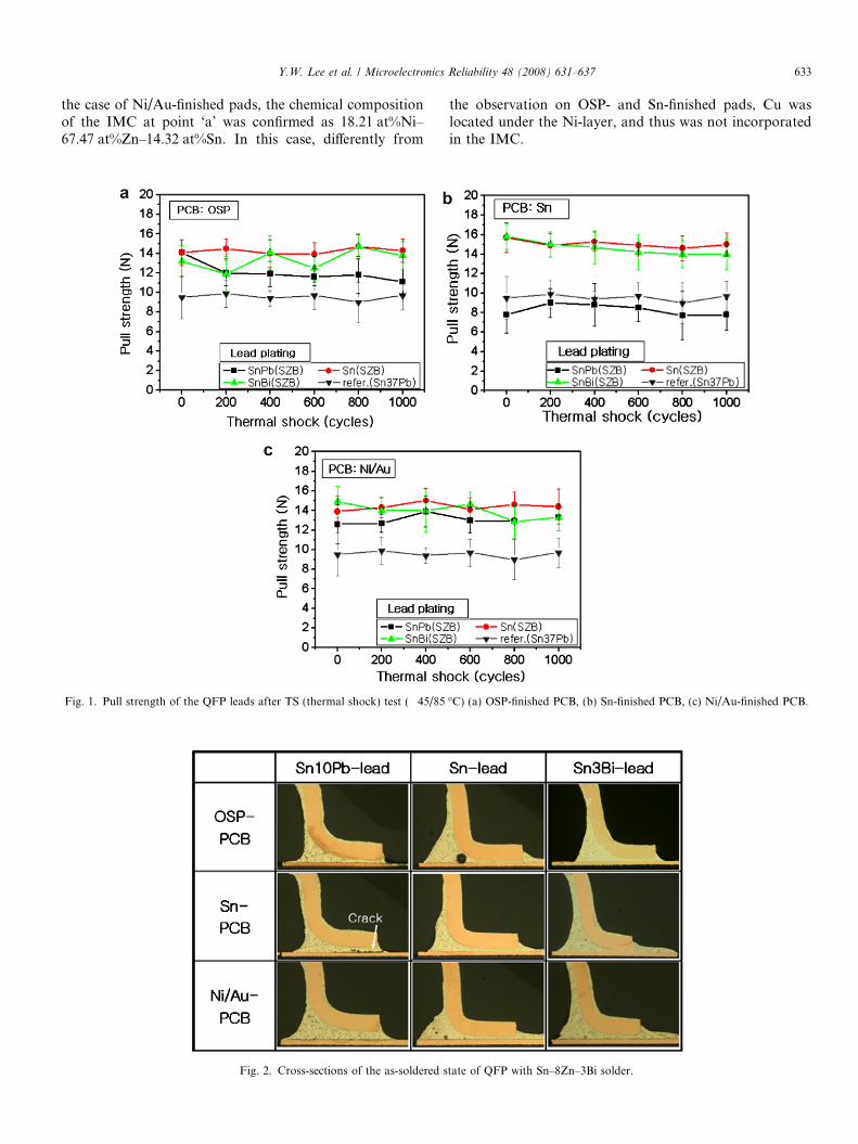
Fig. 1 shows the pull strength data of the QFP solderjoints as a function of thermal shock cycles. For all PCBfinishes and all lead plating compositions, the pullstrengths remained nearly constant with accumulated ther-mal cycles. On the OSP- and Ni/Au-finished PCB’s, thepull strength of leads plated with Sn or Sn–3Bi showed sim-ilar values, although the latter was slightly stronger. Fromthese results, Sn or Sn–3Bi plating gave approximately 30–
50% higher pull strength than the reference solder joint ofSn–37Pb, i.e., about 9.5 N.
For the OSP- and Sn-finished PCB’s, the Sn–10Pb-pla-ted leads had lower strengths (see Fig. 1a and b). Espe-cially in the case of Sn-finish, the Sn–10Pb platingshowed the lowest strength, around 7.5 N, and about53% lower than those of other lead plating compositionsof 15–16 N, and even lower than the reference values.However, in case of Ni/Au-finished PCB (Fig. 1c), thestrength of Sn–10Pb- plated lead was closer to those ofthe other two platings of Sn and Sn–3Bi, and approxi-mately 30% higher than the reference value obtained withSn–37%Pb solder. From the results shown in Fig. 1, it wasfound that the Sn–8Zn–3Bi solder when used on Ni/Aufinished PCB’s gave joint strengths superior to thoseobtained with Sn–37%Pb solder, for all lead plating com-positions employed.
Fig. 2 shows the cross sections of the solder joints in as-soldered state. The leads plated with Sn or Sn–3Bi providedsound joints without cracks for all PCB’s. On the otherhand, in the case of leads plated with Sn–10Pb, crackingwas observed in the as-soldered state for Sn-finishedPCB. This defect was believed to be solidification crack,and the crack was expected to decrease the pull strength,as actually shown in Fig. 1b. However, when the Ni/Au-finished PCB’s were used cracks were hardly found, andthe pull strength had about 30% higher average than thereference value.
Generally Cu6Sn5 and Ni3Sn4 intermetallics are pro-duced on Cu- and Ni-pads, respectively, in soldering withmost Sn-based solder. However, in the case of Sn–Zn sol-der, Cu reacts with Zn instead of with Sn. Thus, Cu–Zncompounds such as Cu5Zn8, and Ni–Zn compounds likeNi5Zn21 are produced on Cu- and on Ni-pads, respectively,when using Sn–Zn based solder [7–9]. Cu5Zn8 has lowerGibbs free energy than Cu6Sn5 specifically �12.10 and�6.26 kJ/mol at 150 �C, respectively, and thus Cu5Zn8 isfound to be more stable between Cu and Sn–Zn based sol-der [10]. The Cu5Zn8 is also known as a stable phase afterthermal cycling compared to CuZn or CuZn2 which hasbeen shown to disappear after aging at 130 �C for 20 h[11] or after 3 thermal cycles [10] between �30 and150 �C, respectively.
Fig. 3 shows interfacial IMCs formed between QFPleads with different plated surfaces and Sn–8Zn–3Bi solderafter 1000 cycles of thermal shock. The composition of theCu–Zn IMC on the Sn–10Pb–plated lead was confirmed as37.51 at%Cu–53.74 at%Zn–8.75 at%Sn, and other interfa-cial IMCs produced between Sn and Sn–3Bi platingshowed similar compositions. This IMC is believed to beCu5Zn8 containing some Sn, and similar IMCs werereported by other researchers [12,13]. In the case of Sn–10Pb plating, small cracks were also observed at thebonded interface.
Interfaces between solder and PCB-pads are illustratedin Fig. 4. IMCs formed on OSP- and Sn-finished pads weresimilar to that shown in Fig. 3, i.e., Cu5Zn8. However, in
Y.W. Lee et al. / Microelectronics Reliability 48 (2008) 631–637 633
the case of Ni/Au-finished pads, the chemical compositionof the IMC at point ‘a’ was confirmed as 18.21 at%Ni–67.47 at%Zn–14.32 at%Sn. In this case, differently from
Fig. 1. Pull strength of the QFP leads after TS (thermal shock) test (�45/85
Fig. 2. Cross-sections of the as-soldered s
the observation on OSP- and Sn-finished pads, Cu waslocated under the Ni-layer, and thus was not incorporatedin the IMC.
�C) (a) OSP-finished PCB, (b) Sn-finished PCB, (c) Ni/Au-finished PCB.
tate of QFP with Sn–8Zn–3Bi solder.

Fig. 3. Interfaces between Sn–8Zn–3Bi solder and leads with different plating after thermal shock testing (�40/85 �C, 1000 cycles).
Fig. 4. Interfaces between Sn–8Zn–3Bi solder and PCB-pads with different plating after thermal shock testing (�40/85 �C, 1000 cycles).
634 Y.W. Lee et al. / Microelectronics Reliability 48 (2008) 631–637
3.2. Low melting temperature phase and cracking
For the Sn-finished pads, the leads plated with Sn–10Pbshowed lower bond strength than the reference value due tocracks. In order to investigate these cracks in more detail,EDS and EPMA analyses were performed. Fig. 5 showsthe result of EPMA analysis for a joint between Sn–
Fig. 5. Low temperature phase observed in the Sn–8Zn–3Bi joints between
10Pb-plated lead and Sn-plated pad after 200 thermalcycles. As shown in Fig. 5 some round phases were pro-duced around the crack (see points ‘a’ and ‘b’). Their com-positions were confirmed as 49.38 wt% Pb–32.58 wt%Sn–18.03 wt%Bi (point a), 51.64 wt% Pb–24.92 wt%Sn–23.43 wt%Bi (point b) by EPMA. It has previously beenpointed out that Sn, Pb and Bi can produce a low melting
Sn–10Pb-plated leads and Sn-plated PCB after 200 cycles of TS test.

Y.W. Lee et al. / Microelectronics Reliability 48 (2008) 631–637 635
temperature phase [14]. For example, 43 wt%Pb–28.5 wt%Bi–28.5 wt%Sn [15] has solidus and liquidus at95 �C and 137 �C, respectively. Other alloys such as50 wt%Pb–30 wt%Sn–20 wt%Bi produced from the IndiumCo., which is a closer composition to point ‘a’ and ‘b’ ofFig. 5, has a melting range of 130–173 �C [15]. Thus thephases observed evidently had a melting temperature wellbelow that of the solder itself, 197 �C. Specifically, duringsolidification of the Sn–8Zn–3Bi, this low melting temper-ature phase exists as a liquid below the solder’s meltingtemperature. Thermal and solidification shrinkage couldreadily make the residual liquid Pb–Sn–Bi phase be tornto produce a crack. Cracking was observed along thebonded interface where the Pb–Sn–Bi phase was found(see Fig. 5). However, the Pb–Sn–Bi phase was also seeninside the bulk solder such as at point ‘c’ and there it didnotproduce any cracking.
The EDS results for the Sn–10Pb leads soldered onpads with Ni/Au-finish are shown in Fig. 6. In this mate-
Fig. 6. Cross section of a Sn–8Zn–3Bi joint betwee
rial combination, cracking was hardly found, and averagelead pull strength was 30% higher than the reference valueas shown in Fig. 1c. On the Ni/Au-pads, the Sn, Pb andBi were much less segregated compared to the behavioron Sn-plated pads (see Fig. 6). Meanwhile, Au dissolvedfrom the pad can produce Au-Pb intermetallics such asAuPb3, AuPb2 or Au2Pb [16,17] with dissolved Pb fromthe lead above 212.5 �C. Au also can produce Au2Bibetween Bi from the solder, although this decomposes to(Au) and (Bi) below 116 �C [18]. These apparently couldsuppress the production of low melting temperaturephases of Pb-Sn-Bi and cracks, which resulted in thestrength increase. Additionally, on the Ni/Au-finishedpads, a Ni–Zn IMC of type Ni5Zn21 was produced alongthe pad interface, which is different from the Cu5Zn8 seenon the Cu/Sn- and Cu/OSP-finished pads. The differencein coefficient of thermal expansion (CTE) of the twoIMCs, Ni5Zn21 versus Cu5Zn8, could also affect crackgeneration.
n Sn–10Pb-plated lead and Ni/Au-plated PCB.
636 Y.W. Lee et al. / Microelectronics Reliability 48 (2008) 631–637
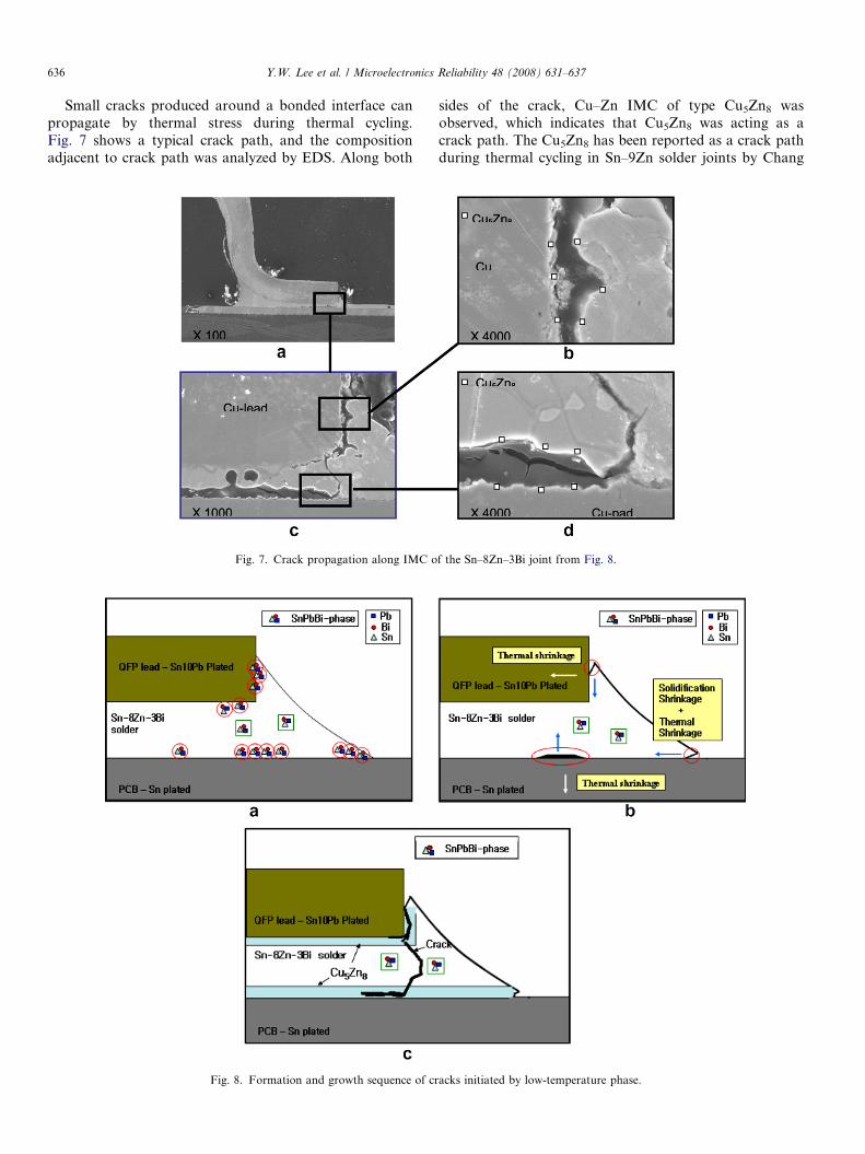
Small cracks produced around a bonded interface canpropagate by thermal stress during thermal cycling.Fig. 7 shows a typical crack path, and the compositionadjacent to crack path was analyzed by EDS. Along both
Fig. 7. Crack propagation along IMC o
Fig. 8. Formation and growth sequence of cr
sides of the crack, Cu–Zn IMC of type Cu5Zn8 wasobserved, which indicates that Cu5Zn8 was acting as acrack path. The Cu5Zn8 has been reported as a crack pathduring thermal cycling in Sn–9Zn solder joints by Chang
f the Sn–8Zn–3Bi joint from Fig. 8.
acks initiated by low-temperature phase.

Y.W. Lee et al. / Microelectronics Reliability 48 (2008) 631–637 637
et al. [10]. In that work, cracks were propagated along Sn–9Zn solder and Cu5Zn8 interfaces by applying five thermalcycles between �30 and 150 �C. The cracking was sug-gested to be due to inferior bonding strength betweenSn–9Zn solder and Cu5Zn8, and thermal stress during thethermal cycles.
From the above results, the cracking phenomenon in thejoints between Sn–8Zn–3Bi and Sn–10Pb-plated leads canbe explained as shown in Fig. 8. Specifically, Pb dissolvedfrom the lead surface and combined with Sn–Bi in the sol-der to form low melting temperature phases such as49.38 wt% Pb–32.58 wt%Sn–18.03 wt%Bi and 51.64 wt%Pb–24.92 wt%Sn–23.43 wt%Bi (Fig. 8a). During solidifica-tion of the solder joint, small cracks were produced by ther-mal and solidification shrinkages by tearing through theliquid films of Pb–Sn–Bi phase (Fig. 8b). The small cracksthen propagated during thermal cycling through the brittleCu–Zn intermetallics due to thermal stress.
4. Conclusions
Sn–8 wt%Zn–3 wt%Bi solder joints with various combi-nations of PCB-finish and QFP lead-plating were investi-gated. The plating on Cu leads was Sn–10 wt%Pb, Sn, orSn–3 wt%Bi and PCB-finish was OSP, Sn or Ni/Au onCu pads. Pull strength before and after thermal shocktreatment was characterized. A low melting temperaturephase found in some joints was investigated. The resultsare as follows:
1. Sn-finished PCB’s soldered to Sn–10Pb plated leadsgave around 20% lower strength than the reference valueof Sn–37Pb solder joints, due to cracking along thejoints.
2. Cracks were initiated due to formation of a low meltingtemperature phase such as 49.38 wt% Pb–32.58 wt%Sn–18.03 wt%Bi, and they propagated through a Cu–ZnIMC layer along the bonded interface.
3. The Ni/Au-finished PCB’s could suppress cracking inthe solder joints even when using the Sn–10Pb platedleads, and showed 30% higher strength than Sn–37%Pb. In this joint Sn, Pb and Bi were less segregatedand phases associated with low melting temperaturewere virtually not observed.
4. The leads plated with Sn or Sn–3Bi showed approxi-mately 30–50% higher pull strength on all compositionsof PCB pad finish than the reference value of Sn–37Pbsolder joints. The pull strengths remained nearlyconstant after thermal cycling for most combinationsof surface platings.
Acknowledgement
This study was financially supported by the Ministry ofCommerce, Industry & Energy, and Samsung Electronics,Korea.
References
[1] Hirose A, Yanagawa H, Ide E, Kobayashi KF. Joint strength andinterfacial microstructure between Sn–Ag–Cu and Sn–Zn–Bi soldersand Cu substrate. Sci Technol Adv Mater 2004;5:267–76.
[2] Zhong WH, Chan YC, Alam MO, Wu BY, Guan JF. Effect ofmultiple reflow processes on the reliability of ball grid array (BGA)solder joints. J Alloys Compd 2006;414:123–30.
[3] Iwanishi H, i Imamura T, Hirose A, Kobayashi KF, Tateyama K,Mori I. Effect of Lead Plating Materials on Properties of QFP JointsUsing Sn-Zn-Bi Solder. In: 8th Symposium on MATE; 2002: p. 277–82.
[4] Amita H, Murase N, Sibuya Y, Nagasaki S, Shoji T. Development ofPb-free Solder Paste in Sn-Zn Alloy System for the Air Reflow. In:6th Symposium on MATE; 2000: p. 319–24.
[5] Hisazato Y, Kato M, Kawakami K, Saito Y. Reliability Assessementof Sn-Ag and Sn-Zn Lead Free Solder Joints by Thermal Fatigue. In:9th Symposium on MATE; 2003: p. 339–44.
[6] Iwanishi H, Imamura T, Hirose A, Tateyama K, Mori I, KobayashiKF. Properties of quad flat package joints using Sn–Zn–Bi solderwith varying lead-plating materials. J Electron Mater 2003;32(12):1540–6.
[7] Shohji Ikuo, Nakmura Takao, Mori Fuminari, Fujiuchi Shinichi.Interface reaction and mechanical properties of lead-free Sn–Znalloy/Cu joints. Mater Trans 2002;43:1797–801.
[8] Chiu MY, Wang SS, Chuang TH. Intermetallic compounds formedduring interfacial reactions between liquid Sn–8Zn–3Bi solders andNi substrates. J Electron mater 2002;31(5):494–9.
[9] Ichitsubo T, Matsubara E, Fujiwara K, Yamaguchi M, Irie H,Kumamoto S, et al. Control of compound forming reaction at theinterface between SnZn solder and Cu substrate. J Alloys Compd2005;392:200–5.
[10] Chang T, Hon M, Wang M, Lin D. Thermal fatigue resistance of theSn-9Zn-xAg lead-free solders/Cu interface. In: IEEE Int’l Sympo OnElectronic Mater Pack; 2002: p. 307–12.
[11] Mei Z et al. Analysis of low-temperature intermetallic growth incopper-tin diffusion couples. Metall Trans A 1992;23:854–7.
[12] Abe Takeshi, Sawada Shoji, Maeda Akira. Interface reaction ofthe Sn-8Zn-3Bi Solder. In: 8th Symposium on MATE; 2002: p.283–8.
[13] Ikeda Haruhiko, Kamada Nobuo. Interface reaction of the Sn–8Zn–3Bi Solder and Cu Electrode. In: 7th Symposium on MATE; 2001: p.487-90.
[14] Yoon SW, Lee HM. A thermodynamic study of phase equilibria inthe Sn-Bi-Pb solder system. Calphad 1998;22(2):167–78.
[15] Mei Zequn, Hua Fay, Judy Glazer. Low Temperature Soldering. In:IEEE/CPMT lnt’l Electronics Manufacturing Technology Sympo-sium; 1997: p. 463–76.
[16] Wang J, Liu HS, Jin ZP. Thermodynamic assessment of the Au–Pbsystem. Comp Coupling Phase Diagrams Thermochem 2004;28:91–95.
[17] Okamoto H, Massalski TB. Binary alloy phase diagram; 1984. p. 293.[18] Okamoto H, Massalski TB. Binary alloy phase diagram; 1984. p. 239.