
Characterisation, Modelling and Design of Bond-Wire ...amsacta.unibo.it/583/1/GM_04_04.pdf ·...
4
Characterisation, Modelling and Design of Bond-Wire Interconnects for Chip-Package Co-Design Arun Chandrasekhar 1 , Serguei Stoukatch 1 , Steven Brebels 1 , Jayaprakash Balachandran 1 , Eric Beyne 1 , Walter De Raedt 1 , Bart Nauwelaers 2 and Anindya Poddar 3 1 MCP-MaRS, IMEC vzw, Kapeldreef 75, 3001, Leuven, Belgium. Phone: +32 16 288228 E-mail: [email protected] 2 Dept. ESAT, K. U. Leuven, Kasteelpark Arenberg 10, 3001, Leuven, Belgium. Phone: +32 16 321114 3 National Semiconductor, 2900 Semiconductor Drive, P.O.Box 58090, Santa Clara, CA, USA. Phone: +1 408 7213130 ABSTRACT — This work is a comprehensive experimental investigation of chip to package wirebond interconnects for chip-package co-design. Wirebonds are interconnect bottlenecks in RF design, but are difficult to avoid due to their low cost and manufacturing ease. We have shown measurements on wirebonds in coplanar configuration with different return paths and also the cross coupling. We have also extracted lumped and distributed models and demonstrate the excellent agreement with measurements atleast upto 15GHz. We have proposed multi-wirebonds as a potential solution for better impedance matching. Different types of inductors with Q-factors of upto 100 have also been illustrated. We show influence of encapsulant on wirebonds and finally we also demonstrate a methodology to extract the time-domain response from S-parameters. I. INTRODUCTION Fig.1. illustrates the gain of a 5.2GHz LNA before and after packaging. The reduction in gain of about 2dB is mainly attributed to the impedance mismatch caused by the wirebond. The LNA was designed without any chip- package co-design considerations. The wirebond has a major contribution in the losses of the chip to board interconnect through the package (fig.2). LNA gain before packaging LNA gain after packaging Fig.1. 5.2GHZ LNA gain before and after packaging. Complete package interconnect Wirebond Only Insertion Loss (dB) Fig .2. Wirebond contribution total interconnect losses. Several publications on wirebonds [1], [2] have shown specific methods to get better impedance match, some including passive compensation techniques [3] (which are realtively narrow band solutions). Others use mathematical methods to derive expressions to model these structures [4]. However, our work complements these contributions by encompassing most chip-package co-design issues that can be addressed with wirebonds through experiments as well and model extraction. An interesting note is that although it is reasonable to assume that flip-chip interconnections give better RF performance over wirebonds, the cost and manufacturing considerations make wirebond applications not easy to replace. This is analogous to developing high-frequency devices with Si and GaAS! Literature is available that show the manufacturing details of wirebonds for RF applications and its comparison with flip-chip. II. WIREBOND MEASUREMENTS We have used MCM-D thin film on glass for the carrier substrate and the test chip due to its excellent RF properties and ease of de-embedding (fig.3). Fig.4 illustrates the measurements made on these bonds with different return paths in CPW configuration. We can also see that the corner bond from the chip to the package is quite lossy compared to bond at the centre of the package. The cross coupling of the wirebond to 4 of its neighbours (all sharing the same return path) is illustrated in fig.5. The coupling is less than 20dB to the adjacent interconnect even at 7GHz. The length of the wirebonds in all the cases is about 2mm. Fig.3. Wirebond test structure on MCM-D thin film on glass. 11th GAAS Symposium - Munich 2003 427
Transcript of Characterisation, Modelling and Design of Bond-Wire ...amsacta.unibo.it/583/1/GM_04_04.pdf ·...
Characterisation, Modelling and Design of Bond-Wire Interconnects for Chip-Package Co-Design
Arun Chandrasekhar1, Serguei Stoukatch1, Steven Brebels1, Jayaprakash Balachandran1, Eric Beyne1, Walter De Raedt1, Bart Nauwelaers2 and Anindya Poddar3
1MCP-MaRS, IMEC vzw, Kapeldreef 75, 3001, Leuven, Belgium. Phone: +32 16 288228 E-mail: [email protected] 2 Dept. ESAT, K. U. Leuven, Kasteelpark Arenberg 10, 3001, Leuven, Belgium. Phone: +32 16 321114
3 National Semiconductor, 2900 Semiconductor Drive, P.O.Box 58090, Santa Clara, CA, USA. Phone: +1 408 7213130
ABSTRACT — This work is a comprehensive experimental investigation of chip to package wirebond interconnects for chip-package co-design. Wirebonds are interconnect bottlenecks in RF design, but are difficult to avoid due to their low cost and manufacturing ease. We have shown measurements on wirebonds in coplanar configuration with different return paths and also the cross coupling. We have also extracted lumped and distributed models and demonstrate the excellent agreement with measurements atleast upto 15GHz. We have proposed multi-wirebonds as a potential solution for better impedance matching. Different types of inductors with Q-factors of upto 100 have also been illustrated. We show influence of encapsulant on wirebonds and finally we also demonstrate a methodology to extract the time-domain response from S-parameters.
I. INTRODUCTION
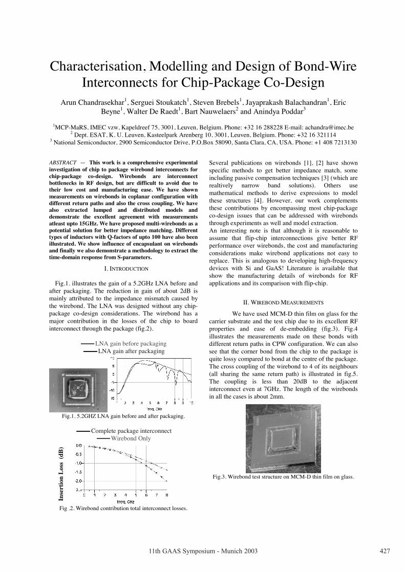
Fig.1. illustrates the gain of a 5.2GHz LNA before and after packaging. The reduction in gain of about 2dB is mainly attributed to the impedance mismatch caused by the wirebond. The LNA was designed without any chip-package co-design considerations. The wirebond has a major contribution in the losses of the chip to board interconnect through the package (fig.2).
LNA gain before packaging LNA gain after packaging
Fig.1. 5.2GHZ LNA gain before and after packaging.
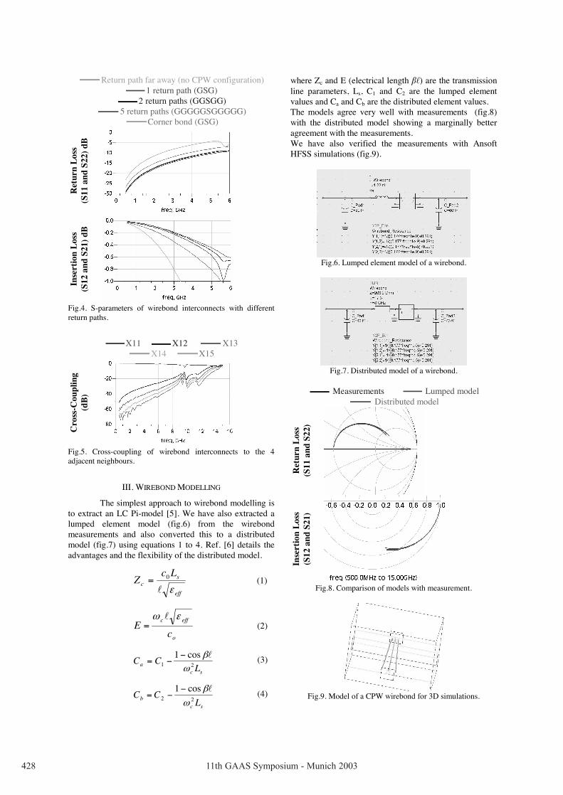
Complete package interconnect
Wirebond Only
Inse
rtio
n L
oss
(dB
)
Fig .2. Wirebond contribution total interconnect losses.
Several publications on wirebonds [1], [2] have shown specific methods to get better impedance match, some including passive compensation techniques [3] (which are realtively narrow band solutions). Others use mathematical methods to derive expressions to model these structures [4]. However, our work complements these contributions by encompassing most chip-package co-design issues that can be addressed with wirebonds through experiments as well and model extraction. An interesting note is that although it is reasonable to assume that flip-chip interconnections give better RF performance over wirebonds, the cost and manufacturing considerations make wirebond applications not easy to replace. This is analogous to developing high-frequency devices with Si and GaAS! Literature is available that show the manufacturing details of wirebonds for RF applications and its comparison with flip-chip.
II. WIREBOND MEASUREMENTS
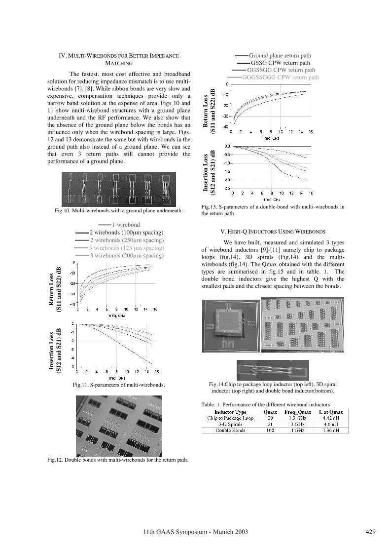
We have used MCM-D thin film on glass for the carrier substrate and the test chip due to its excellent RF properties and ease of de-embedding (fig.3). Fig.4 illustrates the measurements made on these bonds with different return paths in CPW configuration. We can also see that the corner bond from the chip to the package is quite lossy compared to bond at the centre of the package. The cross coupling of the wirebond to 4 of its neighbours (all sharing the same return path) is illustrated in fig.5. The coupling is less than 20dB to the adjacent interconnect even at 7GHz. The length of the wirebonds in all the cases is about 2mm.
Fig.3. Wirebond test structure on MCM-D thin film on glass.
11th GAAS Symposium - Munich 2003 427
Return path far away (no CPW configuration) 1 return path (GSG)
2 return paths (GGSGG) 5 return paths (GGGGGSGGGGG)
Corner bond (GSG)
Ret
urn
Los
s
(S11
and
S22
) dB
In
sert
ion
Los
s
(S12
and
S21
) dB
Fig.4. S-parameters of wirebond interconnects with different return paths.
X11 X12 X13 X14 X15
Cro
ss-C
oupl
ing
(d
B)
Fig.5. Cross-coupling of wirebond interconnects to the 4 adjacent neighbours.
III. WIREBOND MODELLING
The simplest approach to wirebond modelling is to extract an LC Pi-model [5]. We have also extracted a lumped element model (fig.6) from the wirebond measurements and also converted this to a distributed model (fig.7) using equations 1 to 4. Ref. [6] details the advantages and the flexibility of the distributed model.
eff
sc
LcZ
ε�
0= (1)
o
effc
cE
εω �= (2)
sca L
CC21
cos1
ωβ�−
−= (3)
sc
bL
CC22
cos1
ωβ�−
−= (4)
where Zc and E (electrical length ��) are the transmission line parameters, Ls, C1 and C2 are the lumped element values and Ca and Cb are the distributed element values. The models agree very well with measurements (fig.8) with the distributed model showing a marginally better agreement with the measurements. We have also verified the measurements with Ansoft HFSS simulations (fig.9).
Fig.6. Lumped element model of a wirebond.
Fig.7. Distributed model of a wirebond.
Measurements Lumped model
Distributed model
Ret
urn
Los
s
(S11
and
S22
)
Inse
rtio
n L
oss
(S
12 a
nd S
21)
Fig.8. Comparison of models with measurement.
Fig.9. Model of a CPW wirebond for 3D simulations.
11th GAAS Symposium - Munich 2003428
IV. MULTI-WIREBONDS FOR BETTER IMPEDANCE
MATCHING
The fastest, most cost effective and broadband solution for reducing impedance mismatch is to use multi-wirebonds [7], [8]. While ribbon bonds are very slow and expensive, compensation techniques provide only a narrow band solution at the expense of area. Figs 10 and 11 show multi-wirebond structures with a ground plane underneath and the RF performance. We also show that the absence of the ground plane below the bonds has an influence only when the wirebond spacing is large. Figs. 12 and 13 demonstrate the same but with wirebonds in the ground path also instead of a ground plane. We can see that even 3 return paths still cannot provide the performance of a ground plane.
Fig.10. Multi-wirebonds with a ground plane underneath.
1 wirebond
2 wirebonds (100µm spacing) 2 wirebonds (250µm spacing) 3 wirebonds (125 µm spacing) 3 wirebonds (200µm spacing)
Ret
urn
Los
s
(S11
and
S22
) dB
In
sert
ion
Los
s
(S12
and
S21
) dB
Fig.11. S-parameters of multi-wirebonds.
Fig.12. Double bonds with multi-wirebonds for the return path.
Ground plane return path GSSG CPW return path
GGSSGG CPW return path GGGSSGGG CPW return path
Ret
urn
Los
s
(S11
and
S22
) dB
In
sert
ion
Los
s
(S12
and
S21
) dB
Fig.13. S-parameters of a double-bond with multi-wirebonds in the return path
V. HIGH-Q INDUCTORS USING WIREBONDS
We have built, measured and simulated 3 types of wirebond inductors [9]-[11] namely chip to package loops (fig.14), 3D spirals (Fig.14) and the multi-wirebonds (fig.14). The Qmax obtained with the different types are summarised in fig.15 and in table. 1. The double bond inductors give the highest Q with the smallest pads and the closest spacing between the bonds.
Fig.14.Chip to package loop inductor (top left), 3D spiral inductor (top right) and double bond inductor(bottom).
Table. 1. Performance of the different wirebond inductors
11th GAAS Symposium - Munich 2003 429
Fig.15. Q-factor plots of chip-package loop inductor (top) and 3D-spiral (bottom).
VI. INFLUENCE OF ENCAPSULANT ON WIREBONDS
We have studied the influence of gloptop on the wirebond [12]. Fig.16 shows the loss of an encapsulated wirebond with εr=4 and varying tanδ. The influence of tanδ>0.1 is significant.
tanδ=0.001 tanδ=0.01 tanδ=0.1 tanδ=1
Inse
rtio
n L
oss
(dB
)
Fig.16. Loss of encapsulated wirebond (εr=4).
VII. EXTRACTION OF TIME-DOMAIN PERFORMANCE FROM
S-PARAMETERS
With a wealth of S-parameter data available, it is very straightforward to study the time-domain performance of the wirebond interconnects. We have transformed the frequency-domain data to time-domain data. The input signal has a 50ps rise time and a 10� impedance, while the load is a 5pFcapacitance (fig. 17). We can see that the wirebond transforms a typical RC interconnect into an RLC interconnect leading to ringing. It is also very interesting to note that the effect of multiple return paths is insignificant for digital signals which is otherwise for RF analogue signals.
Input 1 Return Path (GSG)
2 Return Paths (GGSGG) 5 Return Paths (GGGGGSGGGGG)
Fig.17. Time-domain performance of wirebonds with multiple return paths.
REFERENCES
[1] A.C.W. Lu, W. Fan, L.L. Wai, L.A. Low, F.X. Ke, K.C. Yip and Y.P. Lim, “Modelling and Characterization of Wirebonding for RF Applications”, in Proceedings of the 52nd IEEE ECTC, May 2002, pp. 905-909.
[2] A. Sutono, N.G. Cafaro, J. Laskar and M.M. Tentzeris, “Experimental Modeling, Repeatability Investigation and Optimization of Microwave Bond Wire Interconnects”, IEEE Transactions on Advanced Packaging, Vol. 24, No. 4, pp. 595-603, Nov. 2001.
[3] T. Krems, W. Haydl, L. Verweyen, M. Schlechtweg, H. Massler and J. Rudiger, “Coplanar Bond Wire Interconnections for Millimeter-wave Applications”, in Proceedings of the IEEE EPEP, Oct. 1995, pp. 178-180
[4] F. Alimenti, U. Goebel and R. Sorrentino, “Quasi Static Analysis of Microstrip Bondwire Interconnects”, in Microwave Symposium Digest MTT-S, Vol. 2, May. 1995, pp. 679-682.
[5] T.P. Budka, “Wide-Bandwidth Millimeter-Wave Bond-Wire Interconnects”, IEEE Transactions on Microwave Theory and Techniques, Vol. 49, No. 4, pp. 715-718, Apr. 2001.
[6] A. Chandrasekhar, S. Brebels, E. Beyne, W. De Raedt, B. Nauwelaers and T. Van Bever, “RF Evaluation of Low-cost Leadless Packages and Development of Distributed Electrical Models”, in Proceedings of the 53rd IEEE ECTC, May 2003, pp. 1550-1558.
[7] F. Alimenti, P. Mezanotte, L. Roselli and R. Sorrentino, “Multi-wire microstrip interconnections: a systematic analysis for the extraction of an equivalent circuit”, in Microwave Symposium Digest MTT-S, Vol. 3, June. 1998, pp. 1929-1932.
[8] F. Alimenti, P. Mezanotte, L. Roselli and R. Sorrentino, “An equivalent circuit for the double bonding wire interconnection”, in Microwave Symposium Digest MTT-S, Vol. 2, June. 1999, pp. 633-636.
[9] S.K Yun and H.Y. Lee, “Wideband Crosstalk analysis of Coupled Bondwires Buried in High-Speed Plastic Packages”, in Proceedings of the 6th IEEE EPEP, Oct. 1997, pp. 91-94.
[10] G. Carchon and W. De Raedt, “Integrated Inductors”, IMEC MCP-MaRS group internal document.
[11] S.J. Kim, Y.G. Lee, S.K. Yun, H.Y. Lee, “Realization of High-Q Inductors using Wirebonding Technology”, in Proceedings AP-ASIC, 1999.
[12] A. Chandrasekhar, S. Brebels, S. Stoukatch, E. Beyne, W. De Raedt and B. Nauwelaers, “The Influence of Packaging Materials on RF Performance”, Microelectronics Reliability Journal, Elsevier Science, Vol. 43/3, pp. 351-357, 2003.
11th GAAS Symposium - Munich 2003430


![SKiN Technology07 ohne.ppt [Kompatibilitätsmodus] · Wire bond-free Wire bonds replaced by sintered SKiN flex layer Double-sided chip sintering for excellent thermal and electrical](https://static.fdocuments.net/doc/165x107/5cef767a88c9937c458d7312/skin-technology07-ohneppt-kompatibilitaetsmodus-wire-bond-free-wire-bonds.jpg)


