
Chapter Chapter ---- 2222 - Shodhgangashodhganga.inflibnet.ac.in/bitstream/10603/31351/9/09_chapter...
29
Chapter Chapter Chapter Chapter - 2 Experimental Techniques Experimental Techniques Experimental Techniques Experimental Techniques for for for for Materials Characterization Materials Characterization Materials Characterization Materials Characterization
-
Upload
truongdien -
Category
Documents
-
view
216 -
download
0
Transcript of Chapter Chapter ---- 2222 - Shodhgangashodhganga.inflibnet.ac.in/bitstream/10603/31351/9/09_chapter...

Chapter Chapter Chapter Chapter ---- 2222
Experimental TechniquesExperimental TechniquesExperimental TechniquesExperimental Techniques for for for for
Materials CharacterizationMaterials CharacterizationMaterials CharacterizationMaterials Characterization
II-1
Experimental Techniques for Materials Characterization
21 Introduction
Materials synthesis and characterization are the most important aspects in
experimental condensed matter physics and materials science research On application
side it is essential to fabricate good quality thin films of materials which are
characterized by variety of techniques The quality of films depends to a great extent on
the film growth method used In addition the proper selection of synthesis parameters
helps to carry out desired properties in the film along with desired applicability
Structure surface morphology grain growth electron transport within material and the
magnetic properties depend on method of synthesis used For the bulk synthesis of
oxides Solid State Reaction (SSR) route has been extensively used and for
nanostructures various methods such as Sol-Gel route Co-precipitation method Citrate
Route Nitrate Route etc are used In laboratory to realize high quality films with desired
properties by precise control on the growth parameter Pulsed Laser Deposition (PLD) is
the most suitable technique In order to characterize the polycrystalline bulk and thin
films of functional oxides various techniques such as X-ray diffraction (XRD) for
structure scanning electron microscopy (SEM) atomic force microscopy (AFM)
transmission electron microscopy (TEM) for microstructure dc four probe resistivity
and I-V measurements for transport and SQUID for magnetic properties are employed
In addition X-ray photoemission spectroscopy (XPS) and Valence band spectroscopy are
used to investigate the detailed electronic structure and doping induced modifications in
the valence band
This chapter presents a detailed description of the experimental techniques used to
characterize the samples prepared during present course of work to study their
functionalities
22 Synthesis Techniques
The synthesis of materials with desired physical properties has been an area of
increasing vitality and importance since many years In the PLD technique dense and
single-phase bulk target is used for the ablation process to make good quality films
Therefore the selection of sample preparation method is a crucial factor The synthesis of
II-2
Experimental Techniques for Materials Characterization
polycrystalline bulk target samples is broadly divided into two categories namely 1)
solid state reaction method and 2) chemical route comprising sol-gel technique nitrate
route co-precipitation technique etc [1-3] In order to prepare a single-phase sample the
synthesis conditions used during any reaction are very important During synthesis the
parameters such as temperature pressure gas flow and time for the reaction are needed to
be varied according to the phase requirements in the sample Mapping of all variables has
to be made to select the conditions which are best suited for each material and phase
221 Solid State Reaction (SSR)
The most common method of synthesizing inorganic solids is the direct reaction
of the component materials at elevated temperatures All the bulk polycrystalline targets
of pure and doped BiFeO3 BaTiO3 SrTiO3 and pure and doped ZnO samples used to
deposit respective films during present course of work were synthesized using SSR
method Mixing of the required oxide or carbonate powders in stoichiometric
proportions calcinations pelletization and sintering of bulk pellet are main steps
involved in SSR method There are two factors namely thermodynamic and kinetic
which are important in solid state reaction the former determines the possibilities of any
chemical reaction to occur by the free energy considerations which are involved while the
later determines the rate at which the reaction occurs [1 4] The atoms diffuse through
the material to form a stable compound having minimum free energy In order to prepare
a single-phase sample the conditions during any reaction are very important During
synthesis the parameters such as temperature pressure gas flow and time for the
reaction are needed to be varied according to the phase requirements in the sample
Figure 21 shows flow chart of SSR method used for synthesis of Multiferroic BiFeO3
As Bi-is volatile element and evaporation temperature of Bi is quite low ~830˚C
formation time and temperature is lower than that generally used in oxide synthesis For
BaTiO3 calcination at 800degC (10 hrs) and 1050degC (5 hrs) were carried out followed by
and final sintering at 1250degC (5 hrs) and for SrTiO3 calcination at 1000degC (24 hrs) then
1200 was followed by sintering at 1250degC (each at 24 hrs)
II-3
Experimental Techniques for Materials Characterization
Figure 21 Flow chart of various steps involved in conventional solid state reaction
route
The advantages of SSR method are listed below
(i) The solid reactants react chemically without the presence of any solvent at high
temperatures yielding a stable product
(ii) The final product in solid form is structurally pure with the desired properties
depending on the final sintering temperatures
(iii) It is environment friendly and no toxic or unwanted waste is produced after
getting final product
222 Sol - Gel technique
Out of several methods for synthesizing polycrystalline ZnO based DMS
materials Sol-Gel is the cost-effective method easy to handle and yields
stoichiometrically predefined compounds It offers a variety of starting materials as
precursors to choose In Sol-Gel technique materials are obtained from chemical solution
via gelation The process involves conversion of monomers into a colloidal solution (sol)
II-4
Experimental Techniques for Materials Characterization
that acts as the precursor for an integrated network (gel) of either discrete particles or
network polymers For nanomaterial synthesis it is necessary to have control over grain
size and also on the phase formation at much lower temperature which can be achieved
by using such chemical methods The different processing stages of Sol-Gel technique
are given below in figure 22
Figure 22 Typical flow chart of Sol-Gel method used for synthesis of pure and Co-
doped ZnO
Key points of the sol-gel method
1 Gelatinous materials as a precursor play a role of an anticoagulant of growing
particles The preparation of monodispersed particles systematically controlled in
mean size and shape have been difficult by conventional methods In this method
under the conditions of high ionic strength growing particles are easily
aggregated and thus uncontrolled in size and shape On the other hand by the sol-
gel method network of a gelatinous precursor prevents the particle aggregation
II-5
Experimental Techniques for Materials Characterization
2 The supersaturation of the system can be kept at a low level by gradual
dissolution of the precursor and the separation of the nucleation and growth stage
is performed The essential conditions to form monodispersed particles are thus
achieved
3 The solid precursor plays an important role as a reservoir of metal ions andor
anions of the product which makes it possible to produce monodispersed particles
in large quantities
During the present course of work polycrystalline Zn1-xCoxO (x = 00 05 and
015) samples were synthesized using sol-gel method Stoichiometric quantities of
Zn(CH3COO)22H2O and Co(CH3COO)24H2O were dissolved in acetic acid and double
distilled water in 11 volume ratio at 90degC resulting in 04 M solution After condensation
and gelation the mixture was dried in air at 150degC and the resulting powder was calcined
at 400degC for 6 hrs and then palletized and sintered at 900degC for 6 hrs
223 Pulsed Laser Deposition (PLD)
For depositing device grade thin films in a laboratory Pulsed Laser Deposition
(PLD) technique is the most suitable and advantageous over other deposition techniques
such as RF Sputtering Metal Oxide Chemical Vapor Deposition (MOCVD) or spray
pyrolysis etc Moreover high energy density of Laser is able to vaporize hardest
materials and therefore useful for the deposition of the oxide materials such as
Superconductors Multiferroics Manganite and Semiconductor [5 6] With the use of
PLD technique one can deposit very high quality thin films with precise control over the
thickness of the film
In the present work for the fabrication of multiferroic thin films and BTO based
FeFET PLD method has been used by employing KrF excimer gas laser using PLD
facility at UGC-DAE CSR Indore National Institute of Technology Hamirpur and
IISER Bhopal The details of optimized conditions and parameters used during PLD are
given in the relevant chapters
A typical PLD system consists a pulsed laser a vacuum chamber a rotating target
holder and a substrate heating block There are several kinds of lasers which are
II-6
Experimental Techniques for Materials Characterization
commercially available such as Excimer lasers (XeCl KrF ArF) are widely used to
deposit high TC superconducting films and other complex oxide films because of the
larger absorption coefficient and small reflectivity of materials at their operating
wavelengths Frequency tripled NdYAG lasers are also effective from the same point of
view
Various steps involved in the PLD process
High power pulsed laser beam is focused inside a vacuum chamber to evaporate
matter from a target surface such that the stoichiometry of the material is preserved in the
interaction As a result a dynamic supersonic jet of plasma (plume) is ejected normal to
the target surface The dynamic plasma plume expands away from the target with a
strong forward directed velocity distribution of the different particles and is transported
over large distances due to quasi free expansion processes and shock wave propagation in
the presence of some background gas [7] The dynamic interactions in the plume can be
modelled using a shock wave model that leads to a quantitative scaling law PD3 =
constant relating the two prominent parameters ie the pressure P and the
target-to-substrate distance D In the case of oxide films oxygen is the most common
background gas For pressures in the range of 100ndash400mTorr the ablated atoms and ions
which attain high kinetic energies (few 10 eV) in the vicinity of the target are
thermalized due the scattering at a particular target-to-substrate distance that is called the
lsquoplume rangersquo (L) and finally condensed on the substrate placed opposite to the target
The plume range L defines two distinct regions in the DndashP diagram for the morphology
and the microstructure and appears as a relevant deposition parameter for the growth of
single crystal films with low roughness and large grains by the PLD technique [8]
Further in most materials the ultraviolet radiation is absorbed by only the outermost
layers of the target up to a depth of ~ 1000 Aring The extremely short laser pulses each
lasting less than 50 ns cause the temperature of the surface to rise rapidly to thousands of
degrees Celsius but the bottom of the target remains virtually unheated close to room
temperature Such un-equilibrium heating produces a flash of evaporated elements that
deposit on the substrate producing a film with composition identical to that of the target
surface Rapid deposition of the energetic ablation species helps to raise the substrate
II-7
Experimental Techniques for Materials Characterization
surface temperature In this respect PLD tends to demand a lower substrate temperature
for crystalline film growth Figure 23 shows the schematic diagram of PLD apparatus
along with target holder substrate holder focusing lens etc which involves evaporation
of a solid target material in an Ultra High Vacuum (UHV) chamber by means of short
and high energy laser pulses
Figure 23 A schematic representation of PLD apparatus
Conventional arrangement for PLD for the synthesis of thin solid films is
characterized by the following features
1 Focused laser beam is directed to the target to ablate the material
2 The target holder is rotated along an axis or (x y) - scanned in the focal plane of
the laser beam to achieve a stationary ablation rate The vacuum chamber is made
of stainless Chamber is evacuated down to 10-6 bar by using a turbo pump
3 Well polished substrate located at a typical separation from the target is stationary
or rotated for homogenization of the deposited material To form a film with
required stoichiometry film growth regimes and the temperature of the substrate
may be selected between room temperature and 1000o C
4 A gas supply is often provided to produce desired chemical reactions during film
growth
II-8
Experimental Techniques for Materials Characterization
Each stage in PLD is critical to the formation of thin films with epitaxial
crystalline structure stoichiometry and smooth surface
Advantages of the PLD technique
(1) The capability for stoichiometric transfer of material from target to substrate ie the
exact chemical composition of a complex material such as YBa2Cu3O7-δ (YBCO) can
be reproduced in the deposited film ie the vaporization is congruent A qualitative
explanation for congruence is that the heating rate provided by pulsed laser irradiation
is so fast that the material removal occurs before the individual components of the
target material can segregate out into low and high vapour pressure components
(2) Relatively high deposition rates typically ~10 nm per minute can be achieved at
moderate laser fluence with film thickness controlled in real time by simply turning
the laser on and off
(3) The fact that a laser is used as an external energy source results in an extremely clean
process without filaments Thus deposition can occur in both inert and reactive
background gases
(4) The use of multiple target holders enables multilayer films to be deposited without the
need to break vacuum when changing between materials
(5) Non requirement of a working gas as in sputter deposition
(6) High flexibility in laboratory scale applications as only small targets (10-12 mm in
diameter with 2-3 mm thick) are needed (in contrast to sputtering where large sized
targets (2Prime - 4Prime diameter and 5-6 mm thick) are required)
(7) Ability to deposit in reactive gas environments (in contrast to conventional
evaporation where hot filaments andor crucibles could contaminate the source
material)
23 Structural Characterizations
It is very essential to study structural properties of any material in order to verify
single phasic nature before carrying out further studies Structural properties are closely
related to the chemical characteristics of the atoms in the material and thus form the basis
II-9
Experimental Techniques for Materials Characterization
on which detailed physical understanding is built Various techniques are used to
ascertain single phasic nature of the samples and detect deviations from the main
structure as well as extracting the actual structure Various techniques have different
advantages and disadvantages and thus complement to each other To study the
crystalline formation of a material X-Ray diffraction measurements are widely used
231 X - ray Diffraction (XRD)
X-ray diffraction (XRD) is non-destructive analytical technique for identification
and quantitative determination of the various crystalline forms known as phases of
compounds present in the powdered and solid samples [9] X-rays are electromagnetic
radiation with typical energies in the range of 100 eV - 100 keV For the purpose of
XRD only short wavelength X-rays ~ 1Aring ie comparable with the size of inter-atomic
distance are used Since the wavelength of X-rays is of the order of 1Aring they are most
ideal for probing the crystalline arrangement of atoms in the polycrystalline bulk as well
as in the thin film forms Generally in the XRD facility the Cu target is used which
emits ~8 KeV X-rays with wavelength of 154Aring X-rays primarily interact with electrons
in atoms
A crystal lattice is a regular array of atoms in space These are arranged in space
to form a series of parallel planes separated from each other by distance d which varies
according to the nature of materials For any crystal planes oriented in different direction
has different d spacing When a monochromatic X-ray beam with wavelength λ is
incident on the lattice planes in the crystal at an angle θ diffraction occurs only when the
distance travelled by rays reflected from successive phases differs by a complete number
lsquonrsquo of λ That is the Braggrsquos condition given by
n λ = 2dsin θ
By varying θ the Braggrsquos law can be satisfied by different lsquodrsquo spacing in a
polycrystalline material (figure 24) Plotting angle position and intensity of the resultant
diffraction peaks produces a pattern which is characteristic of the sample For a sample
containing a mixture of phases the XRD pattern is formed by addition of individual
patterns
II-10
Experimental Techniques for Materials Characterization
Figure 24 Diffraction of X-rays by a crystal planes (Braggrsquos law)
Figure 25 Schematic representation of X-ray diffractometer
Figure 25 represents schematics of X-ray diffractometer The three basic
components of an X-ray diffractometer are x- ray source specimen and x- ray detector
They all lie on the circumference of a circle which is known as the focusing circle The
angle between the plane of the specimen and the X-ray source is θ the Bragg angle The
angle between the projection of the X-ray source and the detector is 2θ For this reason
the X-ray diffraction patterns produced with such geometry are often known as θ-2θ scan
[10]
PAN Analytical PW304060 Xrsquopert PRO X-ray diffractometer (XRD) was used in
the present work to verify the single phasic nature of the samples studied
II-11
Experimental Techniques for Materials Characterization
232 φφφφ - Scan Measurements
Texture measurements are used to determine the orientation distribution of
crystalline grains in the polycrystalline sample One can see textured state of a material
(generally in the form of thin films) A material is called as textured if the grains are
aligned in a preferred orientation along certain lattice planes The texture measurements
have been performed on thin films at a fixed scattering angle and consists of a series of φ
- scans (in-plane rotation around the center of the sample) at different chi-angles (ψ) as
illustrated in the figure 26
Figure 26 Schematic diagram depicting - θ ψ and φ angles during XRD
measurements on films
24 Microscopic Characterizations
Morphological studies are important for understanding the growth and packing
density of grains in thin films or polycrystalline bulk materials There are various
techniques known to explore the science related to surface and morphology of a material
are Scanning Electron Microscopy (SEM) Atomic Force Microscopy (AFM) or
Scanning Probe microscopy (SPM) Tunneling Electron Microscopy (TEM) [11]
241 Scanning Electron Microscopy (SEM)
Scanning electron microscope (SEM) is used for studying the surface topography
microstructure and chemistry of metallic and nonmetallic specimens at magnifications
from 50 up to ~ 100 000 X with a resolution limit lt 10nm (down to ~ 1nm) and a depth
II-12
Experimental Techniques for Materials Characterization
of focus up to several microm (at magnifications ~ 10 000 X) In SEM a specimen is
irradiated by an electron beam and data on the specimen are delivered by secondary
electrons coming from the surface layer of thickness ~ 5nm and by backscattered
electrons emitted from the volume of linear size ~ 05microm Due to its high depth of focus
SEM is frequently used for studying fracture surfaces High resolving power makes SEM
quite useful in metallographic examinations Sensibility of backscattered electrons to the
atomic number is used for the detection of phases of different chemistry Electron
channeling in SEM makes it possible to find the orientation of single crystals by electron
channeling pattern (ECP) or of grains by selected area channeling pattern (SACP)
Figure 27 Schematic block diagram of SEM
242 Atomic Force Microscopy (AFM)
AFM is one of the foremost tools for imaging measuring an
at the nanoscale [figure 2
forces between a tip and the sample [1
surface with a mechanical probe Piezoelectric elements that facilitate tiny but accurate
and precise movements on (electronic) command enable very precise scanning AFM
consists of a microscale cantilever with
the specimen surface [fig
with a tip radius of curvature of the order of nanometers
proximity of a sample surface forces between the tip and the sample lead to a deflection
of the cantilever according to Hookersquos law Depending on the situation forces which are
measured in AFM include mechanical contact force van der waals forces capillary
forces chemical bonding electrostatic forces magnetic forces etc Typically the
deflection is measured using a laser spot reflected from the top surface of the cantilever
into an array of photodiodes
Figure 28 (a) AFM set up (b) Working of AFM
If the tip is scanned at a constant height a risk of tip colliding with the surface
exists causing the damage Hence in most cases a feedback mechanism is employed to
adjust the tip to sample distance to maintain a constant force between the tip and the
sample Traditionally the sample is mounted on a piezoelectric tube which can move the
Experimental Techniques for Materials Characterization
Atomic Force Microscopy (AFM)
AFM is one of the foremost tools for imaging measuring and manipulating matter
28 (a)] AFM is operated by measuring the attractive or repulsive
forces between a tip and the sample [12] The information is gathered by feeling the
surface with a mechanical probe Piezoelectric elements that facilitate tiny but accurate
and precise movements on (electronic) command enable very precise scanning AFM
consists of a microscale cantilever with a sharp tip (probe) at its end which is used to scan
the specimen surface [figure 28 (b)] The cantilever is typically silicon or silicon nitride
with a tip radius of curvature of the order of nanometers When the tip is brought into
surface forces between the tip and the sample lead to a deflection
of the cantilever according to Hookersquos law Depending on the situation forces which are
measured in AFM include mechanical contact force van der waals forces capillary
bonding electrostatic forces magnetic forces etc Typically the
deflection is measured using a laser spot reflected from the top surface of the cantilever
into an array of photodiodes
(a) AFM set up (b) Working of AFM
If the tip is scanned at a constant height a risk of tip colliding with the surface
exists causing the damage Hence in most cases a feedback mechanism is employed to
adjust the tip to sample distance to maintain a constant force between the tip and the
sample Traditionally the sample is mounted on a piezoelectric tube which can move the
II-13
Experimental Techniques for Materials Characterization
d manipulating matter
AFM is operated by measuring the attractive or repulsive
The information is gathered by feeling the
surface with a mechanical probe Piezoelectric elements that facilitate tiny but accurate
and precise movements on (electronic) command enable very precise scanning AFM
a sharp tip (probe) at its end which is used to scan
(b)] The cantilever is typically silicon or silicon nitride
When the tip is brought into
surface forces between the tip and the sample lead to a deflection
of the cantilever according to Hookersquos law Depending on the situation forces which are
measured in AFM include mechanical contact force van der waals forces capillary
bonding electrostatic forces magnetic forces etc Typically the
deflection is measured using a laser spot reflected from the top surface of the cantilever
If the tip is scanned at a constant height a risk of tip colliding with the surface
exists causing the damage Hence in most cases a feedback mechanism is employed to
adjust the tip to sample distance to maintain a constant force between the tip and the
sample Traditionally the sample is mounted on a piezoelectric tube which can move the
II-14
Experimental Techniques for Materials Characterization
sample in the Z direction for maintaining a constant force and the X and Y directions for
scanning the sample Alternatively a tripod configuration of three piezo crystals may be
employed with each responsible for scanning in the X Y and Z directions This
eliminates some of the distortion effects seen with a tube scanner
AFM can be operated in number of modes depending upon the application In
general possible imaging modes are divided into static modes (also called contact
modes) which can be used for Lateral Force Microscopy (LFM) measurements and a
variety of dynamic modes (or non-contact modes) where the cantilever is vibrated
243 Transmission Electron Microscopy (TEM)
In this technique a beam of electrons is transmitted through an ultra thin
specimen interacting with the specimen as it passes through it [13 14] An image is
formed from the electrons transmitted through the specimen magnified and focused by
an objective lens and appears on an imaging screen a fluorescent screen in most TEMs
plus a monitor or on a layer of photographic film or to be detected by a sensor such as a
CCD camera The first TEM was built by Max Knoll and Ernst Ruska in 1931 while the
first commercial TEM was available in 1939
Figure 29 shows the TEM with its components The electron source of the TEM
is at the top where the lensing system focuses the beam onto the specimen and then
projects it onto the viewing screen A TEM is composed of several components which
include a vacuum system in which the electrons travel an electron emission source for
generation of the electron stream a series of electromagnetic lenses as well as
electrostatic plates The latter two allow the operator to guide and manipulate the beam as
required
TEM is used mostly in both material sciencemetallurgy and the biological
sciences In both cases the specimens must be very thin and able to withstand the high
vacuum present inside the instrument Preparation techniques to obtain an electron
transparent region include ion beam milling and wedge polishing The focused ion beam
(FIB) is a relatively new technique to prepare thin samples for TEM examination
Because the FIB can be used to micro-machine samples very precisely it is possible to
II-15
Experimental Techniques for Materials Characterization
mill very thin membranes from a specific area of a sample such as a semiconductor or
metal Materials having dimensions small enough to be electron transparent such as
powders or nanotubes can be quickly produced by the deposition of a dilute sample
containing the specimen onto support grids The suspension is normally a volatile
solvent such as ethanol ensuring that the solvent rapidly evaporates allowing a sample
that can be rapidly analyzed
Figure 29 Schematic of Transmission Electron Microscope (TEM)
II-16
Experimental Techniques for Materials Characterization
25 Spectroscopic Characterizations
252 X - ray Photoelectron Spectroscopy (XPS)
X-ray photoelectron spectroscopy (XPS) is surface analytical technique that
bombards the sample with photonselectrons or ions in order to excite the emission of
photons electrons or ions In XPS the sample is irradiated with low energy (~15 keV)
X-rays in order to provoke the photoelectric effect (figure 210) The energy spectrum of
the emitted photoelectrons is determined by means of a high-resolution spectrometer
XPS offers unique advantages such as unique combination of surface sensitivity and
chemical specificity as well as relatively straight forward means of quantification
Figure 210 Schematic of X-ray Photoelectron Spectroscopy
In the present study X-ray Photoemission Spectroscopy and Valence Band Spectroscopy
(VBS) measurements were carried out using AIPES beamline of UGC DAE CSR at
INDUS ndashI RRCAT Indore Figure 211 shows experimental setup of XUV beamline at
INDUS-I Specifications and other details of beam line are as follows-
Beamline Specifications- A toroidal grating monochromator TGM 2631 with three gratings of 200 600 and
1800 linesmm Wavelength range 60 - 1600 (8 - 200 eV) Pre - and Post - mirrors of toroidal type Final spot size at sample lt 1 mm2 Angle integrated photoelectron spectroscopy station Average resolving power of 300
Figure 211 Experimental setup of XUV beamline at INDUS
Energywavelength range
Wave length range Gratings
Linesmm Coating
540-1600 Adeg 200
180-540 Adeg 600
60-180 Adeg 1800
UHV compatible angle integrated photoelectron spectrometer comprising of
a Hemispherical analyser having mean radius of 95mm
b Ion gun for sample cleaning
c Sample manipulator with XYZ motion
d Sample heating up to 900oC and cooling up
e Sample preparation chamber with quick load lock and sample transfer system
Photoelectron Spectrometer
The experimental station of
spectrometer which was designed and fabricated indigenously This consists of (1) the
energy analyzer (2) the experimental chamber with in
arrangement of the sample mounted on XYZ sa
Experimental Techniques for Materials Characterization
Experimental setup of XUV beamline at INDUS-I
Energywavelength range
Gratings Linesmm Coating
Spectral resolution
lDl measured with discharge source
200 Pt 650 at 584 Adeg
600 Pt 950 at 304 Adeg
1800 Pt
UHV compatible angle integrated photoelectron spectrometer comprising of
Hemispherical analyser having mean radius of 95mm
Ion gun for sample cleaning
Sample manipulator with XYZ motion
Sample heating up to 900oC and cooling up to LN2 temperature
Sample preparation chamber with quick load lock and sample transfer system
Photoelectron Spectrometer
The experimental station of AIPES beamline is an angle integrated photoelectron
spectrometer which was designed and fabricated indigenously This consists of (1) the
(2) the experimental chamber with in-situ heating and cooling
arrangement of the sample mounted on XYZ sample manipulator (3) sample preparation
II-17
Experimental Techniques for Materials Characterization
Spectral resolution
measured with discharge source
UHV compatible angle integrated photoelectron spectrometer comprising of
Sample preparation chamber with quick load lock and sample transfer system
beamline is an angle integrated photoelectron
spectrometer which was designed and fabricated indigenously This consists of (1) the
situ heating and cooling
mple manipulator (3) sample preparation
II-18
Experimental Techniques for Materials Characterization
chamber equipped with quick load-lock magnetic sample transfer system ion gun for
controlled etching of the sample and diamond file type scrapper and (4) the associated
electronics as well as the data acquisition system A brief description of the spectrometer
is given below A schematic diagram of the typical photoelectron spectrometer is shown
in figure 212
Figure 212 Schematic of typical XPS spectrometer
The electron energy analyzer is the most important part of the spectrometer The
complete analyzer system consists of the following parts the electrostatic lens the
hemispherical elements and the detector The lens is a three-piece cylindrical system The
lens is used to transport the electrons from the emission area to the hemispherical
analyzer through the entrance slit of the analyzer plate The most common configuration
of the three-piece lens is an einzel lens in which the outer electrodes are held at the
ground potential and beam focusing is achieved by varying the potential on the centre
electrode This type of lens is commonly used in electron spectrometers Each cylinder is
machined out of stainless steel and mirror polished and coated with gold for excellent
transmission of the beam All the pieces are then mounted inside a stainless steel shield
which in turn is mounted on the analyzer plate
The inner and outer hemispheres of the analyzer are machined out of aluminum in
a numerically controlled universal milling machine to an accuracy better than
II-19
Experimental Techniques for Materials Characterization
+0001mm The surfaces are then polished and coated with gold This ensures uniform
potential energy surfaces and prevents surface charging The hemispheres are mounted on
a fringe plate (H-plate) also machined out of aluminum which has entrance and exit
slits slit width can be varied from 1mm to 3mm in discrete steps of 1 mm The entire
analyzer assembly is mounted such that the inner hemisphere outer hemisphere and the
H-plate are insulated from touching each other by using teflon washers and bushes
Electrons are focused to the entrance slit of the analyzer through the entrance aperture by
the lens system Energy dispersion takes place as the electrons travel through the
electrostatic field between the inner and outer hemispheres There are six concentric rings
made out of stainless steel mounted on the H-plate to correct the fringe field which
improves the resolution of the analyzer These rings are positioned within the annular
space (gap between the two hemispheres) equidistantly The inner and the outer
hemispheres have a radius of 65 mm (r1) and 125 mm (r2) respectively The mean radius
of the analyzer is 95 mm and the annular space is 60 mm
The detection of electrons is carried out by applying a high voltage to the channel
electron multiplier (X719BL Philips make) mounted at the exit slit of the analyzer A
single turn of enameled copper wire is carefully mounted surrounding the analyzer This
can be used to fine-tune the focusing of the beam into the analyzer entrance slit A Mu
metal shield surrounds the analyzer and lens for shielding it from earthrsquos magnetic field
The spectrometer chamber is also shielded by the mu metal
The electronics system consists of a spectrometer control unit to provide various
voltages to the energy analyzer a pulse amplifier to amplify the detected signal a rate
meter to count the number of electrons per second The total electronics system is
interfaced to an IBM compatible personal computer A windows based software program
is then run which scans the spectrometer and acquires the data and stores it in a file for
further analysis
The function of the analyzer is as follows When the sample is kept at ground
potential electrons ejected from a state with binding energy Eb are emitted with a true
kinetic energy Ek given by Ek = hν- Eb -f where f is the work function of the sample
The ejected electrons pass through the lens and are then retarded by an amount R
II-20
Experimental Techniques for Materials Characterization
determined by the lens voltages before entering the analyzer The retardation of kinetic
energy to pass energy is necessary to achieve the required resolution Therefore the
electrons which have been transmitted by the analyzer with a retardation R and pass
energy HV would have a kinetic energy given by the equation-
E = R + HV + f ---- (1)
Here the H which is 1403 for our analyzer is the analyzer constant
The inner hemisphere is applied a positive potential with respect to the outer The
analyzer is scanned by varying the retard voltage applied to the analyzer plate while
holding the analyzer pass energy constant This ensures a constant resolution for the
whole range of kinetic energies The absolute resolution is usually measured as the full
width at half-maximum (FWHM) height of a chosen observed peak
Resonant Photoemission Spectroscopy
If the core electron is resonantly excited to the high energy continuum well above
the absorption threshold (as in the process of X-ray photoemission spectroscopy) this
type of PES is denoted as resonant X-ray emission spectroscopy (RPES) [15] In order to
perform RPES measurements high intensity tunable X-ray source is required Resonance
phenomenon occurs in photoemission when the energy of incident photons is close to the
energy difference between a fully occupied core level and a partially occupied shell such
as 3d shell in transition metals 4f shell in rare earths or 5f shell in actinides In the
present study RPES study on Co-doped ZnO has been carried out using AIPES beamline
of UGC-DAE CSR at INDUS-I RRACAT Indore The resonance process in the case of
Cobalt can be interpreted as originating from the interference between the normal
photoemission process and the indirect process induced by the photo induced excitation
The reactions involved in the resonance phenomena are as follows direct process
Co3p63d7 + hνrarr Co3p63d6 + e and indirect process Co3p63d7 + hνrarr [Co3p53d8]
followed by the emission of a Co 3d electron through a super Koster-Kroning decay
[Co3p53d8] rarr Co3p63d6 + e The interference between the two channels of
photoemission leads to an increase in the photoemission intensity as the photon energy is
swept through the Co 3p-3d threshold
II-21
Experimental Techniques for Materials Characterization
26 Transport Characterizations
The knowledge about the electrical properties of the bulk materials thin films and
artificial devices is essential in determining their applicability and usefulness The
resistivity must be measured accurately since its value is critical from application point of
view The samples in the present thesis work were characterized for their electrical and
magneto transport properties by the DC four-probe resistivity technique as described
below
261 Current vs Voltage (I-V) measurements
Since last few years the efforts have been made on the fabrication of devices
based on oxide thin films and multilayers having potential applications To understand
the transport behavior of such single crystalline and polycrystalline thin film and devices
I-V characteristics emerge as a most comprehensive tool In addition many important
parameters can be extracted from I-V measurements For practical application of the
insulating oxide films the leakage current controls the charge retention property which is
very important affecting factor for the consideration in practical memory application
Figure 213 Current Perpendicular in plane (CPP) geometry for I-V measurements
During the present work the I-V behavior of the oxide thin film heterostructures
amp p-n junction diodes was studied using the dc two probe method by varying the
applied voltage and observing the variation in current Figure 213 show the schematic of
contact geometry used in the I-V measurements All the measurements were taken from
the AuAg electrodes For multiferroic thin films hysteretic I-V measurements were
taken at various temperatures and varying plusmnVmax Effect of doping concentration and
thickness variation has been studied on hysteretic behavior of I-V curves
27 Electrical Characterizations
271 Dielectric measurements
Dielectric is an electrical
field When a dielectric is placed in an electric field
the material but only slightly shift from their average equilibrium positions
causing dielectric polarization
displaced toward the field and negative charges sh
creates an internal electric field which reduces the overall field within the dielectric
itself If a dielectric is composed of weakly bonded molecules these molecules not only
become polarized but also reorient so tha
While the term insulator implies low
used to describe materials with a
called the dielectric constant
obstruction while the term dielectric is used to indicate the energy storing capacity of the
material (by means of polarization) A common yet notable example of a dielectric is
the electrically insulating material between the metallic plates of a
Figure 214 Schematic diagram of a parallel plate capacitor with dielectric spacer
Dielectric constant
of the material The temperature and frequency dependent capacitance was measured
using Agilent 4284A precision LCR meter In order to avoid any parasitic impedance
Experimental Techniques for Materials Characterization
Electrical Characterizations
Dielectric measurements
is an electrical insulator that can be polarized by an applied
When a dielectric is placed in an electric field electric charges do not flow through
the material but only slightly shift from their average equilibrium positions
dielectric polarization Because of dielectric polarization positive charges are
displaced toward the field and negative charges shift in the opposite direction This
creates an internal electric field which reduces the overall field within the dielectric
If a dielectric is composed of weakly bonded molecules these molecules not only
become polarized but also reorient so that their symmetry axis aligns to the field
While the term insulator implies low electrical conduction lsquodielectricrsquo is typically
used to describe materials with a high polarizability The latter is expressed by a number
dielectric constant The term insulator is generally used to indicate electrical
obstruction while the term dielectric is used to indicate the energy storing capacity of the
material (by means of polarization) A common yet notable example of a dielectric is
y insulating material between the metallic plates of a capacitor
Schematic diagram of a parallel plate capacitor with dielectric spacer
Dielectric constant for the sample can be calculated by measuring the capacitance
of the material The temperature and frequency dependent capacitance was measured
A precision LCR meter In order to avoid any parasitic impedance
II-22
Experimental Techniques for Materials Characterization
by an applied electric
electric charges do not flow through
the material but only slightly shift from their average equilibrium positions
Because of dielectric polarization positive charges are
ift in the opposite direction This
creates an internal electric field which reduces the overall field within the dielectric
If a dielectric is composed of weakly bonded molecules these molecules not only
t their symmetry axis aligns to the field
lsquodielectricrsquo is typically
The latter is expressed by a number
The term insulator is generally used to indicate electrical
obstruction while the term dielectric is used to indicate the energy storing capacity of the
material (by means of polarization) A common yet notable example of a dielectric is
capacitor (figure 214)
Schematic diagram of a parallel plate capacitor with dielectric spacer
for the sample can be calculated by measuring the capacitance
of the material The temperature and frequency dependent capacitance was measured
A precision LCR meter In order to avoid any parasitic impedance
II-23
Experimental Techniques for Materials Characterization
shielded test leads were used for electrical connection from the analyzer to sample First
films were heated at 100degC for 1hour for homogenization of charge carrier and remove
the moisture content For making a capacitor type arrangement sample surfaces were
coated using silver paste which act as a good contact for measuring dielectric properties
The value of the dielectric constant (εrsquo) was calculated using formula
εrsquo = CC0 helliphelliphelliphelliphelliphelliphellip (21)
where εrsquo is the real part of dielectric constant C is the capacitance of the material
inserted between the electrodes and C0 is the capacitance of the medium as air or no
medium between the electrodes The C0 for the parallel plate capacitor can be calculated
using the following relation
C0 = ε0 A t helliphelliphelliphelliphelliphelliphellip (22)
where ε0 is permittivity in vacuum ~ 885 times 10-12 C2N m2 t is the thickness of the
sample and A is the area of the specimen in sqm
Now using eq (1) amp (2) the dielectric constant can be calculated as
εrsquo = C times t ε0 A helliphelliphelliphelliphelliphelliphellip (23)
The imaginary component of dielectric constant (εrsquorsquo) is calculated using the formula
εrsquorsquo = εrsquo tanδ helliphelliphelliphelliphelliphelliphellip (24)
where tanδ is loss tangent proportional to the lsquolossrsquo of energy from the applied field into
the sample in which energy is dissipated into heat and therefore known as a dielectric
loss
272 Polarization - Electric field (P - E loop) measurements
Ferroelectricity is usually defined as irreversibility of the spontaneous
polarization by an applied electric field P - E hysteresis loop is the essential
characteristic of ferroelectric materials From the P - E loop one can get the information
about the saturation polarization (PS) remnant polarization (Pr) and coercive field (EC)
which help us to understand the effect of applied electric field with frequency Figure
215 shows the schematic diagram of typical P - E hysteresis loops observed in
II-24
Experimental Techniques for Materials Characterization
ferroelectric materials Depending on types of samples shape of the P - E loop changes
according to their ferroelectric behaviour There are four types of shape (i) linear P - E
loop (ii) resistive capacitor loop (iii) lossy hysteresis and (iv) non-linear hysteresis loop
Figure 215 Typical types of ferroelectric loops (a) linear P - E loop (b) resistive P - E
loop (c) lossy P - E loop and (d) non-linear P - E loop
The most often quoted method of hysteresis loop measurement is based on a
Sawyer and Tower circuit in which the field applied across the sample is attenuated by a
resistive divider and the current is integrated into charge by virtue of a large capacitor in
series with the sample Both these voltages are then fed into the X and Y axes of an
oscilloscope to generate the P - E loop The applied voltage is usually a sinusoidal at
mains frequency Also there are commercially available high voltage amplifiers which
allow frequencies other than those tied to the mains frequency and also enable waveforms
other than sine waves to be used Sine waves are most often used since these can be
easily produced however a triangle wave drive is more attractive for frequency
dependent measurements since dEdt is constant
II-25
Experimental Techniques for Materials Characterization
28 Magnetic characterizations (M-T amp M - H)
SQUID magnetometer is the most widely used instrument for magnetic
characterization in material science It has been proved as a boon to elucidate many
interesting results in superconductors manganites and ferrites [16] The superconducting
quantum interference device (SQUID) consists of two superconductors separated by thin
insulating layers to form two parallel Josephson junctions The device may be called as a
magnetometer to detect incredibly small magnetic fields The SQUID has as its active
element one or more Josephson junctions
Figure 216 A schematic diagram of SQUID magnetometer
A Josephson junction is a weak link between two superconductors that can
support a supercurrent below a critical value Ic The special properties of the Josephson
junction cause the impedance of the SQUID loop to be a periodic function of the
magnetic flux threading the SQUID so that a modulation signal supplied to the bias
II-26
Experimental Techniques for Materials Characterization
current is used with a lock-in detector to measure the impedance and to linearize the
voltage-to-flux relationship The net result is that a SQUID functions as a flux-to-voltage
converter with unrivaled energy sensitivity In most practical systems in use today the
SQUID is located inside a small cylindrical superconducting magnetic shield in the
middle of a liquid helium Dewar and shown in the figure 218 Superconducting pickup
coils typically configured as gradiometers that detect the difference in one component of
the field between two points are located at the bottom of the Dewar and the sample is
placed beneath the magnetometer The rest of the hardware is designed to minimize
helium boil off eliminate rf interference and to not contribute Johnson noise or distort
any external a c fields [16] The sensitivity of SQUID is associated with measuring
changes in magnetic field of one flux quantum as shown in figure 217
Figure 217 Variation of magnetic flux with change in voltage `
If a constant biasing current is maintained in the SQUID device the measured
voltage oscillates with the changes in phase at the two junctions which depends upon the
change in the magnetic flux The flux change can be evaluated by counting the
oscillations It may be noted that the sensitivity of SQUID is 10-14 Tesla which is
incredibly large to measure any magnetic signal
II-27
Experimental Techniques for Materials Characterization
REFERENCE
[1] EM Engler Chem Technol 17 542 (1987)
[2] SX Dou HK Liu AJ Bourdillon JP Zhou NX Tan XY Sun CC Sorrell
J Am Ceram Soc 71C 329 (1998)
[3] CJ Brinkered and GW Scherer ldquoSol-Gel Sciencerdquo Academic Press Inc Boston
(1990)
[4] AR West ldquoSolid State Chemistry and its Applicationsrdquo John Wiley and Sons
(1984)
[5] SP Gapanov BM Luskin NN Salaschenko Sov Tech Phys Lett 5 210
(1979)
[6] SP Gapanov A Gudkov AA Fraerman Sov Tech Phys Lett 27 1130
(1982)
[7] DB Geohegan Thin Solid Films 220 138 (1992)
[8] M Strikovski and J H Miller Appl Phys Lett 73 1733 (1998)
[9] BD Cullity and SR Stock ldquoElements of X-ray diffractionrdquo Prentice all Inc
New Jersey (2001)
[10] Doctoral Dissertation ldquoNovel room temperature ferromagnetic semiconductorsrdquo
by Amita Gupta LBNL-56596 eScholarship Repository University of California
(2004)
[11] EN Kaufmann ldquoCharacterization of Materialsrdquo John Wiley and Sons (2003)
[12] G Binning CF Quate and Ch Gerber Phys Rev Lett 56 930 (1986)
[13] Encyclopedia of Materials characterization Surface interface thin films Editors
CR Brundle CA Evans Jr and S Wilson Butterworth Heinemann (U S A)
(1992)
[14] D Shindo and T Oikawa ldquoAnalytical Electron Microscopy for Materials
Sciencerdquo Springer-Verlag Tokyo (2002)
II-28
Experimental Techniques for Materials Characterization
[15] A Kotani and S Shin Rev of Modern Phys 73 203 (2001)
[16] SQUID Manual by Quantum Design
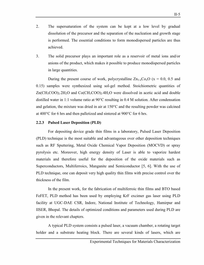

II-28
Experimental Techniques for Materials Characterization
[15] A Kotani and S Shin Rev of Modern Phys 73 203 (2001)
[16] SQUID Manual by Quantum Design