Chapter 8 Sequential Circuits - Philadelphia University Chapter8... · (Clocked) RS flip-flop With...
39
28-05-2014 1 Philadelphia University Faculty of Information Technology Department of Computer Science Computer Logic Design By Dareen Hamoudeh 1 Dareen Hamoudeh Chapter 8 Sequential Circuits
Transcript of Chapter 8 Sequential Circuits - Philadelphia University Chapter8... · (Clocked) RS flip-flop With...
28-05-2014
1
Philadelphia University
Faculty of Information Technology
Department of Computer Science
Computer Logic Design
By
Dareen Hamoudeh
1Dareen Hamoudeh
Chapter 8Sequential Circuits
28-05-2014
2
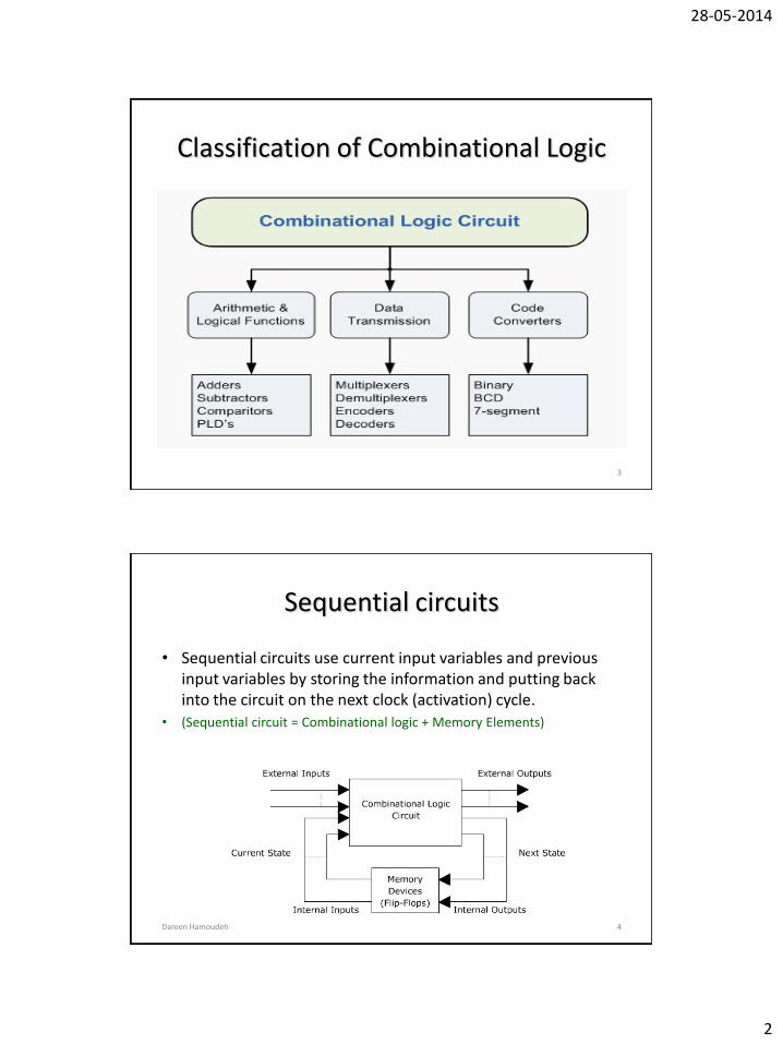
Classification of Combinational Logic
3
Sequential circuits
• Sequential circuits use current input variables and previous input variables by storing the information and putting back into the circuit on the next clock (activation) cycle.
• (Sequential circuit = Combinational logic + Memory Elements)
4Dareen Hamoudeh
28-05-2014
3
Memory Element
• A Memory Element: logic device that can store a binary information, this binary information defines the state of the circuit.
• Can remember value indefinitely, or change its value on command from its inputs.
• Current State of a sequential Circuit: Value stored in memory elements (value of state variables).
• State transition: A change in the stored values in memory elements thus changing the sequential circuit from one state to another state.
• Types of sequential circuits depending on the timing of their signals:
– Synchronous
– Asynchronous
5Dareen Hamoudeh EECC341 - Shaaban
Memory Elementstates
• The output Q of the memory element represents the value stored in the memory element. This is also called the statevariable of the memory elements.
• A memory element can be in one of two possible states:
– Q = 0 (the memory element has 0 stored), also said be in state 0.
– Q =1 (the memory element has 1 stored), also said to be in state 1.
• A sequential circuit that contains n memory elements could be in one of a maximum of 2n states at any given time depending on the stored values in the memory elements.
6EECC341 - Shaaban
28-05-2014
4
Memory Elementcommands
• The commands to the memory element formed by its input(s) may include:
– Set: Store 1 (Q=1) in the memory element.
– Reset: Store 0 (Q=0) in the memory element.
– Flip: Change stored value from 0 to 1 or from 1 to 0.
– Hold value: Memory value does not change.
• Memory Element state transition: A change in the stored value from 0 to 1, or from 1 to 0 such as that caused by a flip command.
7EECC341 - Shaaban
Synchronous Sequential circuits
• Synchronous Sequential circuits must employ signals that affect the memory elements only at discrete instance of time using pulses of limited duration, where one pulse represents logic 1 and another pulse represents logic 0.
• Synchronization is achieved by a timing device called master-clock generator.
• (Synchronous Sequential Circuits: Sequential circuits that have a clock signal as one of its inputs)
• Synchronous Sequential circuits that use clock pulses in the input of memory elements are called clocked sequential circuits.
8Dareen Hamoudeh EECC341 - Shaaban
28-05-2014
5
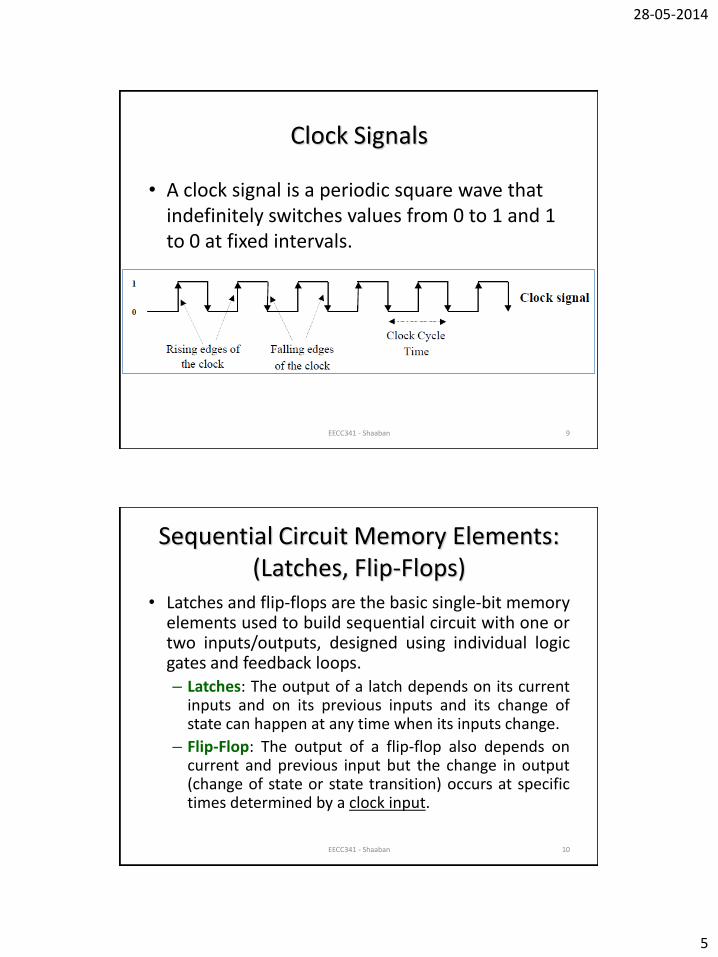
Clock Signals
• A clock signal is a periodic square wave that indefinitely switches values from 0 to 1 and 1 to 0 at fixed intervals.
9EECC341 - Shaaban
Sequential Circuit Memory Elements: (Latches, Flip-Flops)
• Latches and flip-flops are the basic single-bit memoryelements used to build sequential circuit with one ortwo inputs/outputs, designed using individual logicgates and feedback loops.– Latches: The output of a latch depends on its current
inputs and on its previous inputs and its change ofstate can happen at any time when its inputs change.
– Flip-Flop: The output of a flip-flop also depends oncurrent and previous input but the change in output(change of state or state transition) occurs at specifictimes determined by a clock input.
10EECC341 - Shaaban
28-05-2014
6
Clocked sequential circuits.
• Memory elements used here are called flip-flops.
• These circuits are binary cells that can store one bit of information.
11Dareen Hamoudeh
Flip-Flops
• Flip-flop types:
– Basic flip flop circuit (latch).
– RS flip-flop.
– D flip-flop.
– JK flip-flop.
– T flip-flop.
12Dareen Hamoudeh
28-05-2014
7
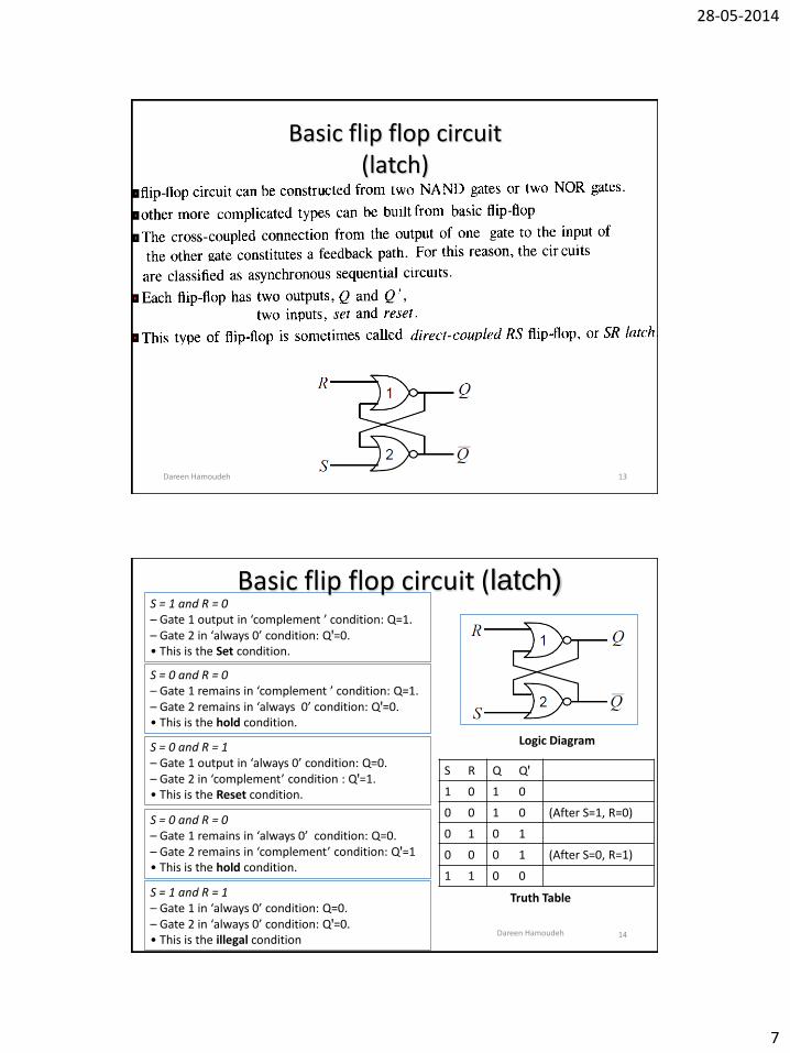
Basic flip flop circuit(latch)
13Dareen Hamoudeh
S R Q Qꞌ
1 0 1 0
0 0 1 0 (After S=1, R=0)
0 1 0 1
0 0 0 1 (After S=0, R=1)
1 1 0 0
S = 1 and R = 0– Gate 1 output in ‘complement ’ condition: Q=1.– Gate 2 in ‘always 0’ condition: Qꞌ=0.• This is the Set condition.
S = 0 and R = 0– Gate 1 remains in ‘complement ’ condition: Q=1.– Gate 2 remains in ‘always 0’ condition: Qꞌ=0.• This is the hold condition.
S = 0 and R = 1– Gate 1 output in ‘always 0’ condition: Q=0.– Gate 2 in ‘complement’ condition : Qꞌ=1.• This is the Reset condition.
S = 0 and R = 0– Gate 1 remains in ‘always 0’ condition: Q=0.– Gate 2 remains in ‘complement’ condition: Qꞌ=1• This is the hold condition.
S = 1 and R = 1– Gate 1 in ‘always 0’ condition: Q=0.– Gate 2 in ‘always 0’ condition: Qꞌ=0.• This is the illegal condition
Truth Table
Logic Diagram
Basic flip flop circuit (latch)
14Dareen Hamoudeh
28-05-2014
8
Basic flip flop circuit
(latch)
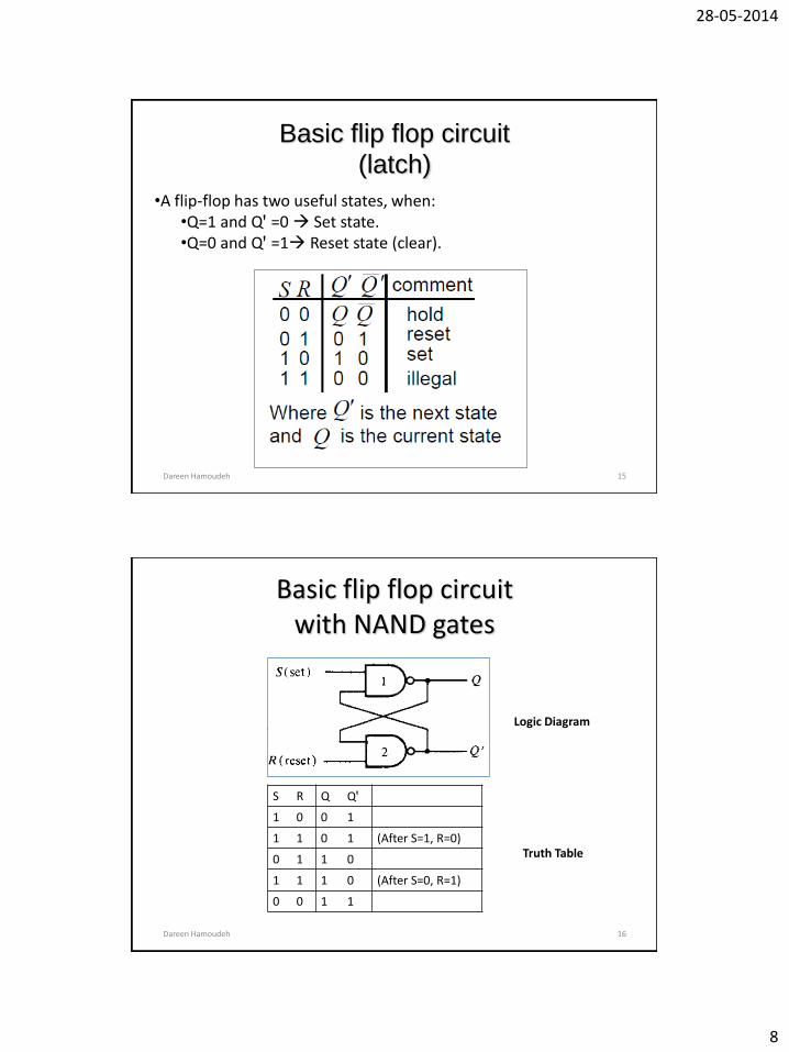
•A flip-flop has two useful states, when:•Q=1 and Qꞌ =0 Set state.•Q=0 and Qꞌ =1 Reset state (clear).
15Dareen Hamoudeh
Basic flip flop circuitwith NAND gates
S R Q Qꞌ
1 0 0 1
1 1 0 1 (After S=1, R=0)
0 1 1 0
1 1 1 0 (After S=0, R=1)
0 0 1 1
Truth Table
Logic Diagram
16Dareen Hamoudeh
28-05-2014
9
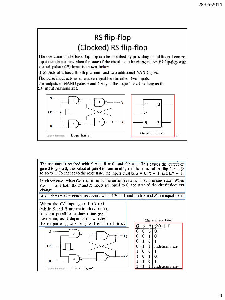
RS flip-flop(Clocked) RS flip-flop
17Dareen Hamoudeh
18Dareen Hamoudeh
28-05-2014
10
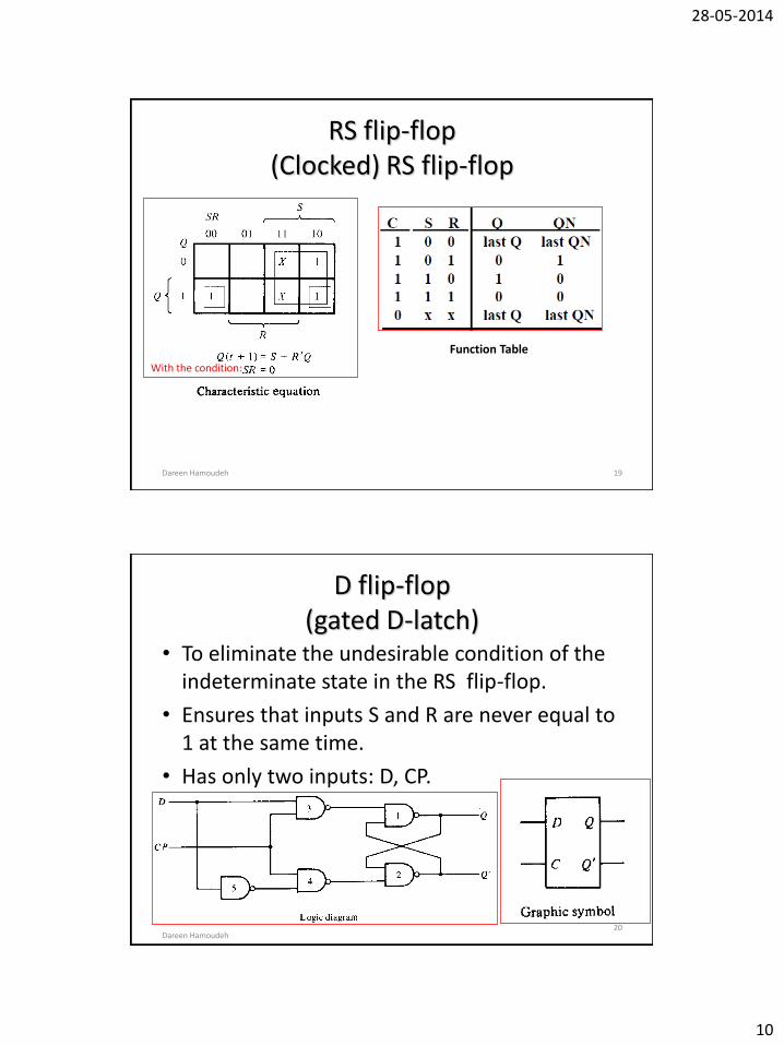
RS flip-flop(Clocked) RS flip-flop
With the condition:
Function Table
19Dareen Hamoudeh
D flip-flop(gated D-latch)
• To eliminate the undesirable condition of the indeterminate state in the RS flip-flop.
• Ensures that inputs S and R are never equal to 1 at the same time.
• Has only two inputs: D, CP.
20Dareen Hamoudeh
28-05-2014
11
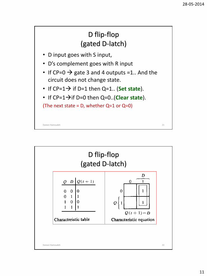
D flip-flop(gated D-latch)
• D input goes with S input,
• D’s complement goes with R input
• If CP=0 gate 3 and 4 outputs =1.. And the circuit does not change state.
• If CP=1 if D=1 then Q=1.. (Set state).
• If CP=1if D=0 then Q=0..(Clear state).
(The next state = D, whether Q=1 or Q=0)
21Dareen Hamoudeh
D flip-flop(gated D-latch)
22Dareen Hamoudeh
28-05-2014
12
D flip-flop
• D flip-flop refers to its ability to hold data into its internal storage.
• The CP input sometimes called G (gate) because it enables the gated latch to make possible data entry into the circuit.
23Dareen Hamoudeh
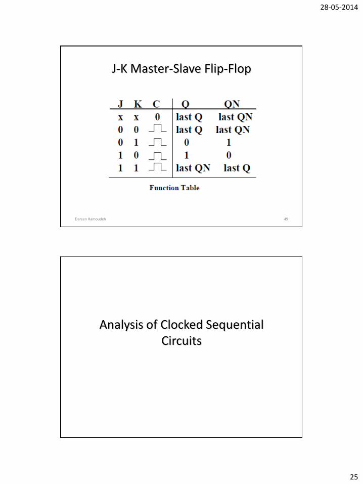
JK Flip-Flop
• It is a refinement of RS flip-flop where the indeterminate state is defined here.
• Input J is set and K is Reset.
• When J=K=1 the flip-flop switches to its complement (last state is inverted):
– if Q=1 it switches to Q=0.
– if Q=0 it switches to Q=1.
24Dareen Hamoudeh
28-05-2014
13
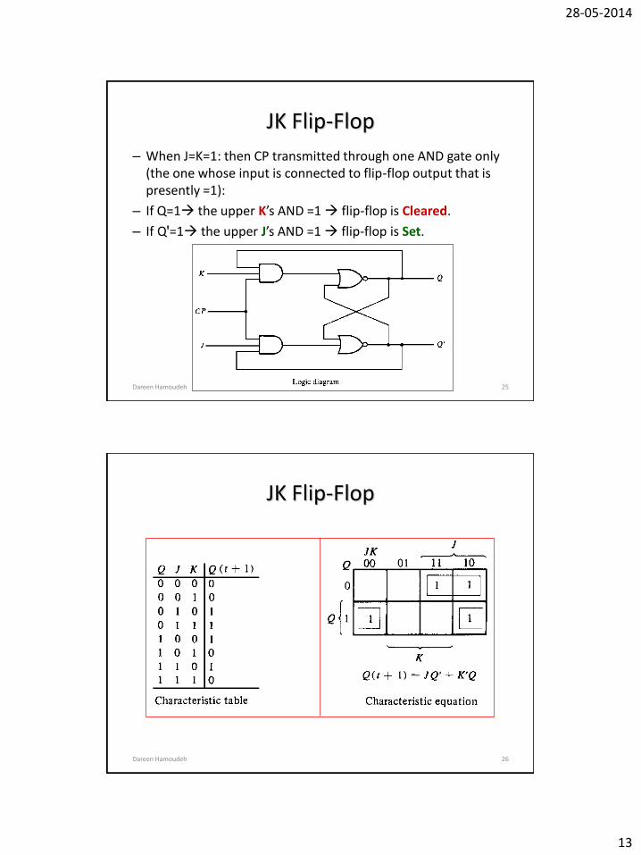
JK Flip-Flop
– When J=K=1: then CP transmitted through one AND gate only (the one whose input is connected to flip-flop output that is presently =1):
– If Q=1 the upper K’s AND =1 flip-flop is Cleared.
– If Qꞌ=1 the upper J’s AND =1 flip-flop is Set.
25Dareen Hamoudeh
JK Flip-Flop
26Dareen Hamoudeh
28-05-2014
14
JK Flip-Flop
• Problems:– Because of the feedback connection in the JK flip-flop, CP
will still =1 while J=K=1 will cause the output to complement again and repeat complementing until the CP=0.• To avoid this, CP must have shorter time duration (pulse width)
than the flip-flop delay time.
• This is a restrictive requirement.
• Solution:
• JK flip-flop is not constructed like this.
• Restriction on pulse width can be eliminated with a Master-Slave or Edge-Triggered construction.
27Dareen Hamoudeh
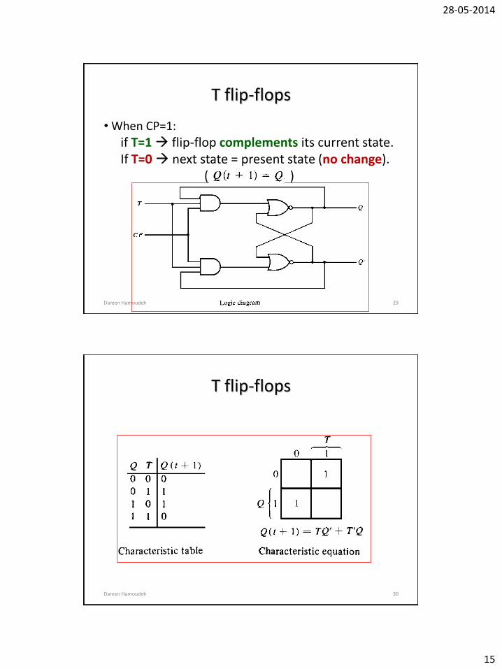
T flip-flops
• Is a single-input version of JK flip-flop.
• It is obtained from JK flip-flop when both inputs are tied together.
• T refers to the ability of flip-flop to Toggle or complement its state.
28Dareen Hamoudeh
28-05-2014
15
T flip-flops
• When CP=1:
if T=1 flip-flop complements its current state.If T=0 next state = present state (no change).
( )
29Dareen Hamoudeh
T flip-flops
30Dareen Hamoudeh
28-05-2014
16
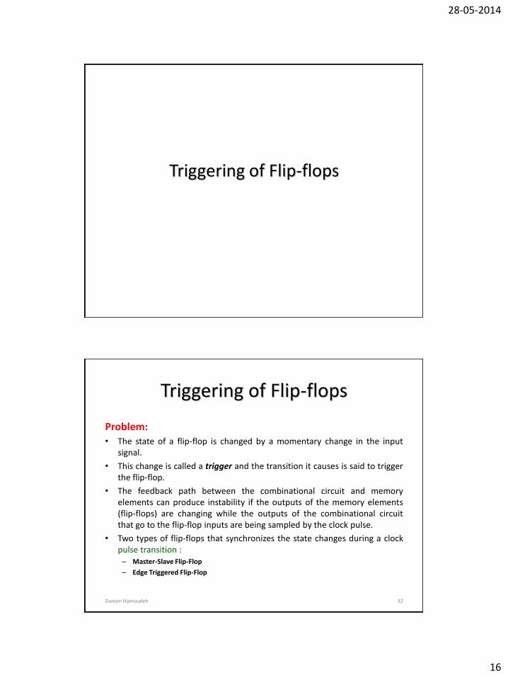
Triggering of Flip-flops
Triggering of Flip-flops
Problem:• The state of a flip-flop is changed by a momentary change in the input
signal.
• This change is called a trigger and the transition it causes is said to triggerthe flip-flop.
• The feedback path between the combinational circuit and memoryelements can produce instability if the outputs of the memory elements(flip-flops) are changing while the outputs of the combinational circuitthat go to the flip-flop inputs are being sampled by the clock pulse.
• Two types of flip-flops that synchronizes the state changes during a clockpulse transition :– Master-Slave Flip-Flop
– Edge Triggered Flip-Flop
32Dareen Hamoudeh
28-05-2014
17
Triggering of Flip-flops
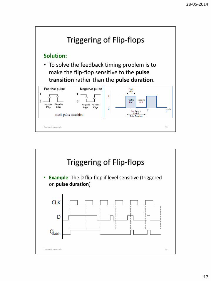
Solution:
• To solve the feedback timing problem is to make the flip-flop sensitive to the pulse transition rather than the pulse duration.
33Dareen Hamoudeh
Triggering of Flip-flops
• Example: The D flip-flop if level sensitive (triggered on pulse duration)
34Dareen Hamoudeh
28-05-2014
18
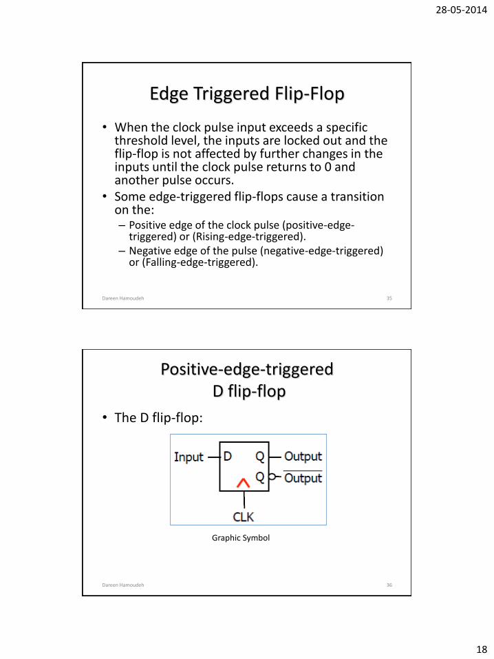
Edge Triggered Flip-Flop
• When the clock pulse input exceeds a specific threshold level, the inputs are locked out and the flip-flop is not affected by further changes in the inputs until the clock pulse returns to 0 and another pulse occurs.
• Some edge-triggered flip-flops cause a transition on the:– Positive edge of the clock pulse (positive-edge-
triggered) or (Rising-edge-triggered).– Negative edge of the pulse (negative-edge-triggered)
or (Falling-edge-triggered).
35Dareen Hamoudeh
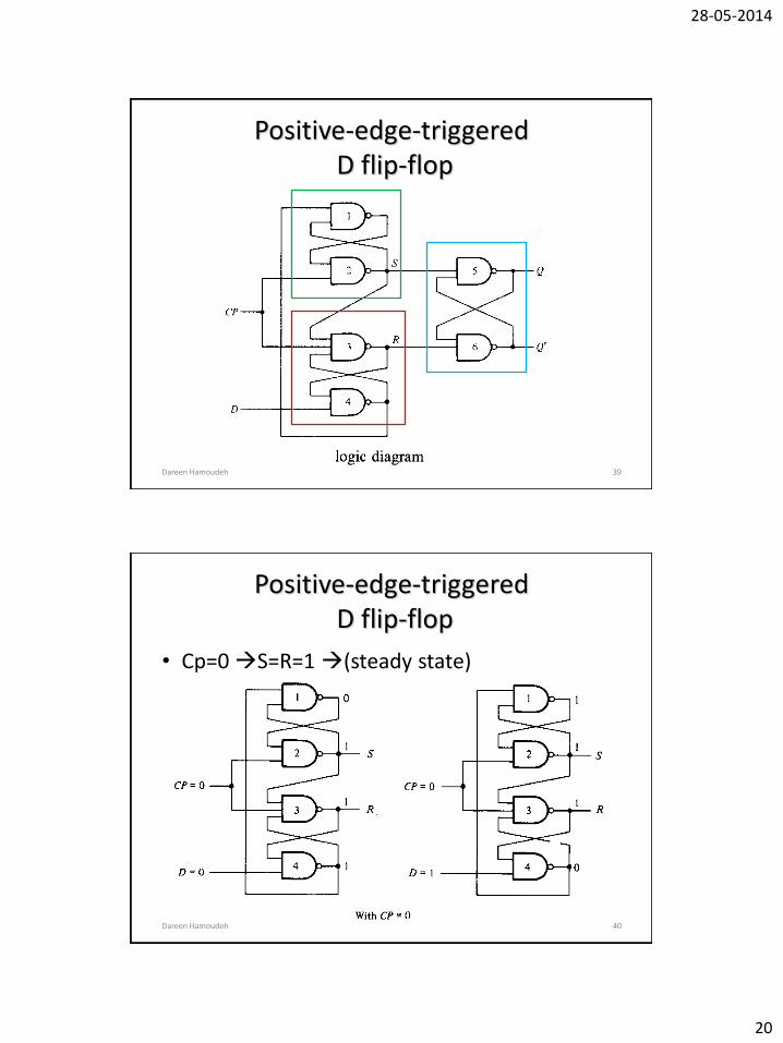
Positive-edge-triggeredD flip-flop
• The D flip-flop:
Dareen Hamoudeh 36
Graphic Symbol
28-05-2014
19
Positive-edge-triggeredD flip-flop
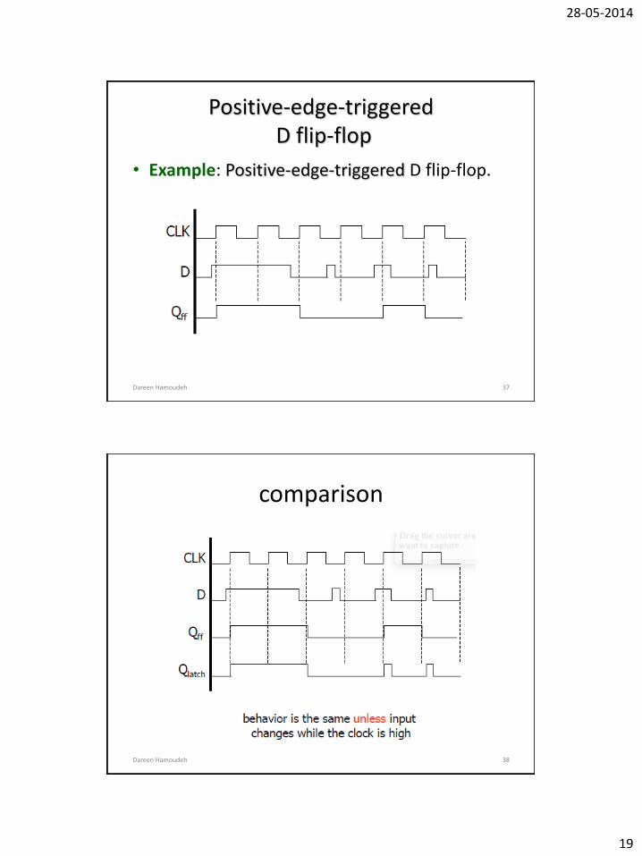
• Example: Positive-edge-triggered D flip-flop.
Dareen Hamoudeh 37
comparison
Dareen Hamoudeh 38
28-05-2014
20
Positive-edge-triggeredD flip-flop
Dareen Hamoudeh 39
Positive-edge-triggeredD flip-flop
• Cp=0 S=R=1 (steady state)
Dareen Hamoudeh 40
28-05-2014
21
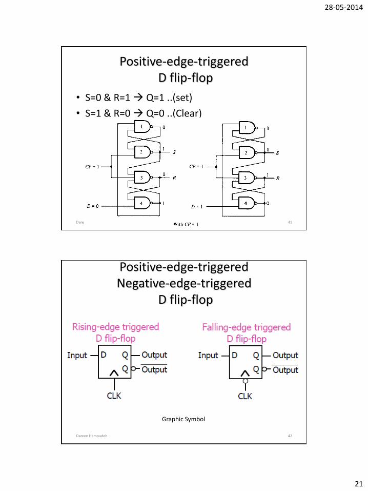
Positive-edge-triggeredD flip-flop
• S=0 & R=1 Q=1 ..(set)
• S=1 & R=0 Q=0 ..(Clear)
Dareen Hamoudeh 41
Positive-edge-triggeredNegative-edge-triggered
D flip-flop
Dareen Hamoudeh 42
Graphic Symbol
28-05-2014
22
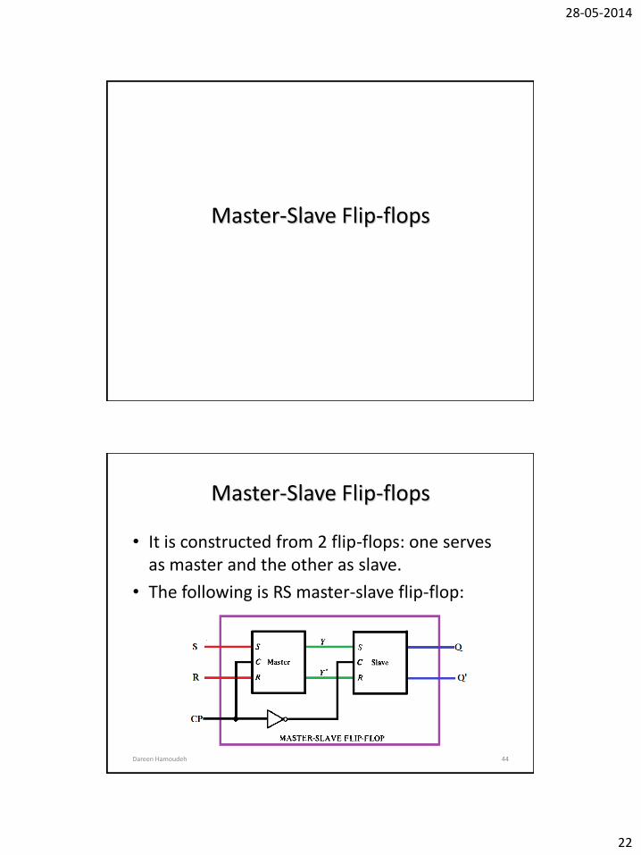
Master-Slave Flip-flops
Master-Slave Flip-flops
• It is constructed from 2 flip-flops: one serves as master and the other as slave.
• The following is RS master-slave flip-flop:
Dareen Hamoudeh 44
28-05-2014
23
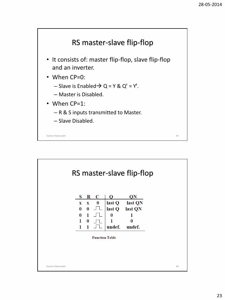
RS master-slave flip-flop
• It consists of: master flip-flop, slave flip-flop and an inverter.
• When CP=0:
– Slave is Enabled Q = Y & Qꞌ = Yꞌ.
– Master is Disabled.
• When CP=1:
– R & S inputs transmitted to Master.
– Slave Disabled.
Dareen Hamoudeh 45
RS master-slave flip-flop
Dareen Hamoudeh 46
28-05-2014
24
RS master-slave flip-flop
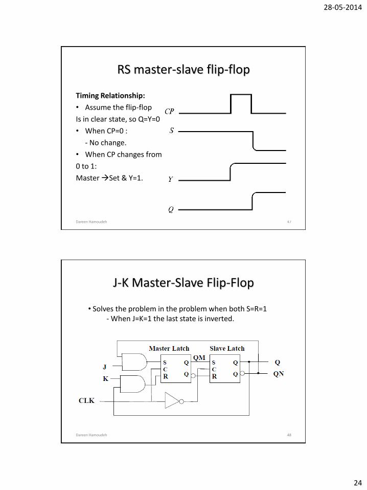
Timing Relationship:
• Assume the flip-flop
Is in clear state, so Q=Y=0
• When CP=0 :
- No change.
• When CP changes from
0 to 1:
Master Set & Y=1.
Dareen Hamoudeh 47
J-K Master-Slave Flip-Flop
Dareen Hamoudeh 48
• Solves the problem in the problem when both S=R=1- When J=K=1 the last state is inverted.
28-05-2014
25
J-K Master-Slave Flip-Flop
Dareen Hamoudeh 49
Analysis of Clocked Sequential Circuits
28-05-2014
26
Analysis of Clocked Sequential Circuits
• Behavior of sequential circuit is determined by: – Inputs.– Outputs.– Flip-flop state.
• (Outputs & Next state ) are functions to ( inputs & present state).
• Analysis is to obtain:– table, diagram for time sequence of (inputs, outputs,
states),– write Boolean expressions (to describe behavior of
circuit) that include necessary time sequence.
Dareen Hamoudeh 51
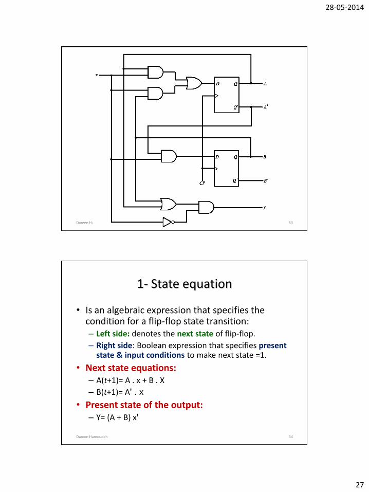
• The following clocked sequential circuit consists of:
– Two D flip-flops A and B,
– Input x.
– Output Y.
Dareen Hamoudeh 52
Sequential circuit example
28-05-2014
27
Dareen Hamoudeh 53
1- State equation
• Is an algebraic expression that specifies the condition for a flip-flop state transition:– Left side: denotes the next state of flip-flop.
– Right side: Boolean expression that specifies present state & input conditions to make next state =1.
• Next state equations:– A(t+1)= A . x + B . X
– B(t+1)= Aꞌ . x
• Present state of the output:– Y= (A + B) xꞌ
Dareen Hamoudeh 54
28-05-2014
28
2- State Table
• Enumerates the sequence of inputs, outputs and flip-flop states. It consists of 4 sections :– Current state .– Input.– Next state (must satisfy the state equation).– Output.
• First: we should list all possible combinations of current states and inputs.
• Second: next-state and output values are determined from state equations.
• Number of rows (combinations) = 2 m + n , where:– m :number of flip-flops.– n: number of inputs.
Dareen Hamoudeh 55
2- State Table
In the example there are:
• Two flip-flops, so m=2.
• One input (x), so n=1.
• Then we have 23 combinations
Dareen Hamoudeh 56
28-05-2014
29
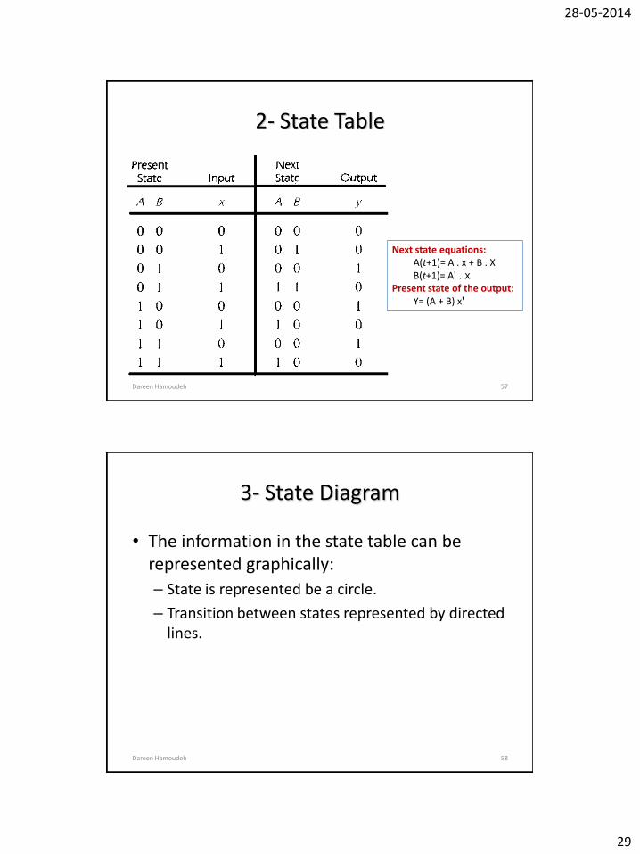
2- State Table
Dareen Hamoudeh 57
Next state equations:A(t+1)= A . x + B . XB(t+1)= Aꞌ . x
Present state of the output:Y= (A + B) xꞌ
3- State Diagram
• The information in the state table can be represented graphically:
– State is represented be a circle.
– Transition between states represented by directed lines.
Dareen Hamoudeh 58
28-05-2014
30
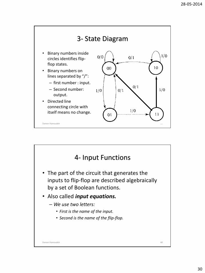
3- State Diagram
• Binary numbers inside circles identifies flip-flop states.
• Binary numbers on lines separated by “/”:
– first number : input.
– Second number: output.
• Directed line connecting circle with itself means no change.
Dareen Hamoudeh 59
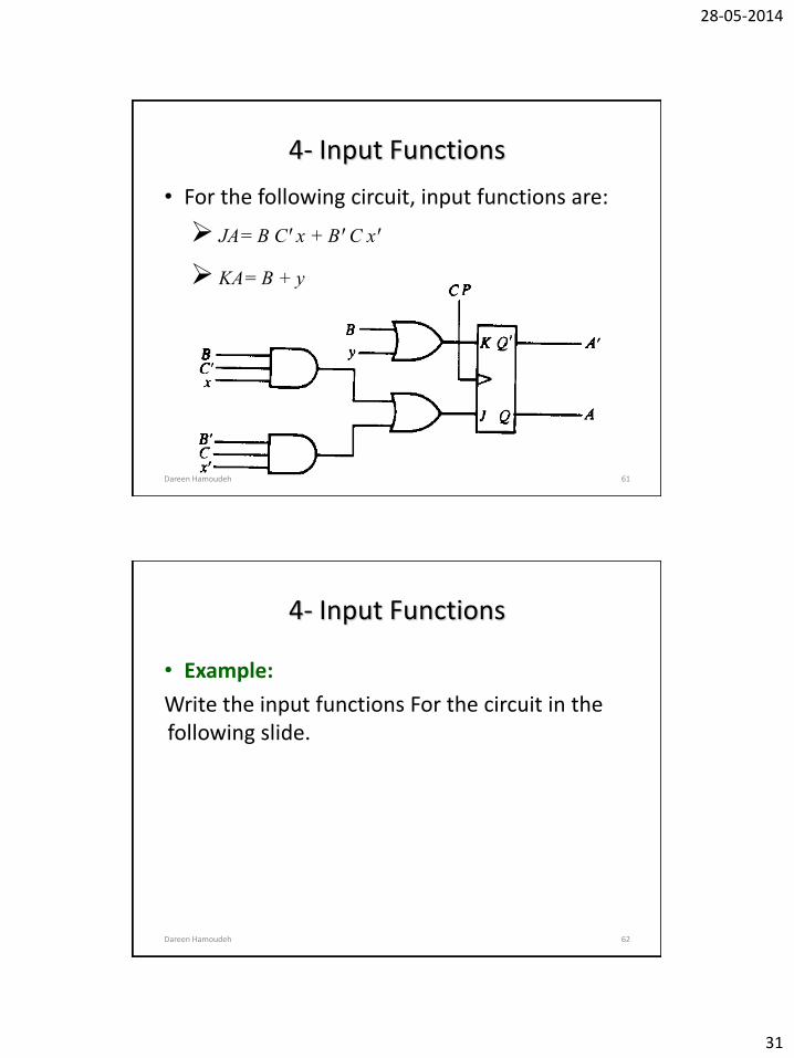
4- Input Functions
• The part of the circuit that generates the inputs to flip-flop are described algebraically by a set of Boolean functions.
• Also called input equations.
– We use two letters:
• First is the name of the input.
• Second is the name of the flip-flop.
Dareen Hamoudeh 60
28-05-2014
31
4- Input Functions
• For the following circuit, input functions are:
JA= B Cꞌ x + Bꞌ C xꞌ
KA= B + y
Dareen Hamoudeh 61
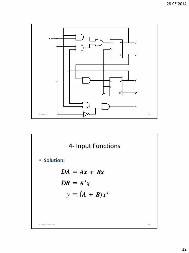
4- Input Functions
• Example:
Write the input functions For the circuit in the following slide.
Dareen Hamoudeh 62
28-05-2014
32
Dareen Hamoudeh 63
4- Input Functions
• Solution:
Dareen Hamoudeh 64
28-05-2014
33
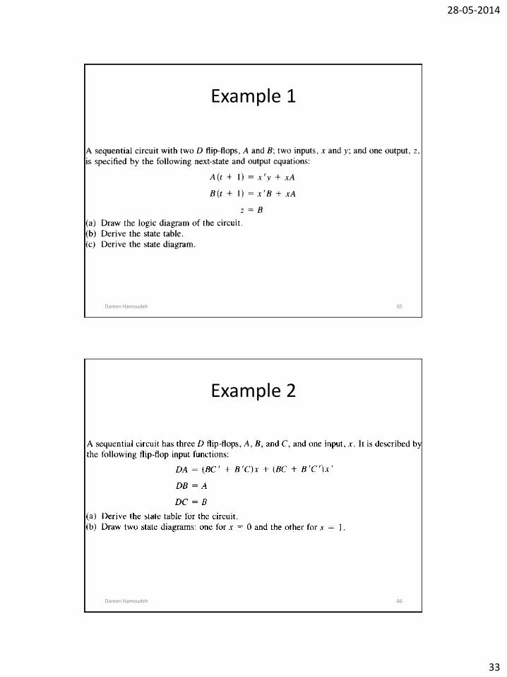
Example 1
Dareen Hamoudeh 65
Example 2
Dareen Hamoudeh 66
28-05-2014
34
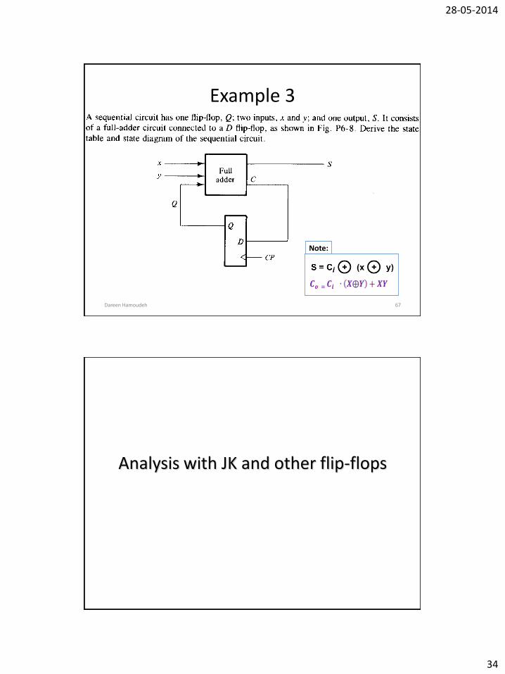
Example 3
Dareen Hamoudeh 67
Note:
Analysis with JK and other flip-flops
28-05-2014
35
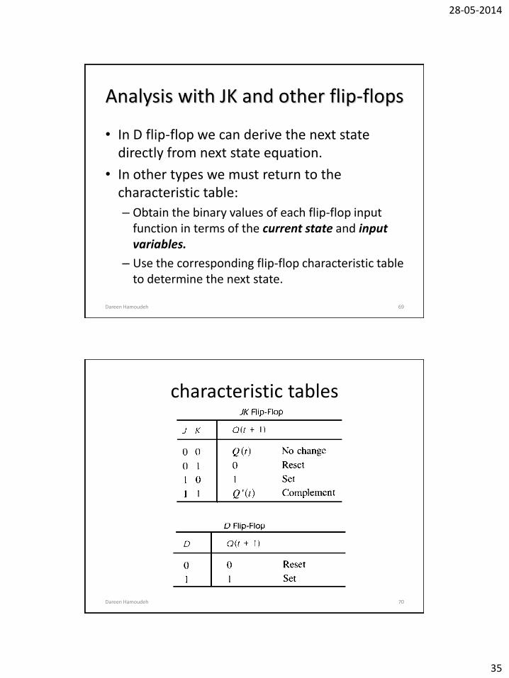
Analysis with JK and other flip-flops
• In D flip-flop we can derive the next state directly from next state equation.
• In other types we must return to the characteristic table:
– Obtain the binary values of each flip-flop input function in terms of the current state and input variables.
– Use the corresponding flip-flop characteristic table to determine the next state.
Dareen Hamoudeh 69
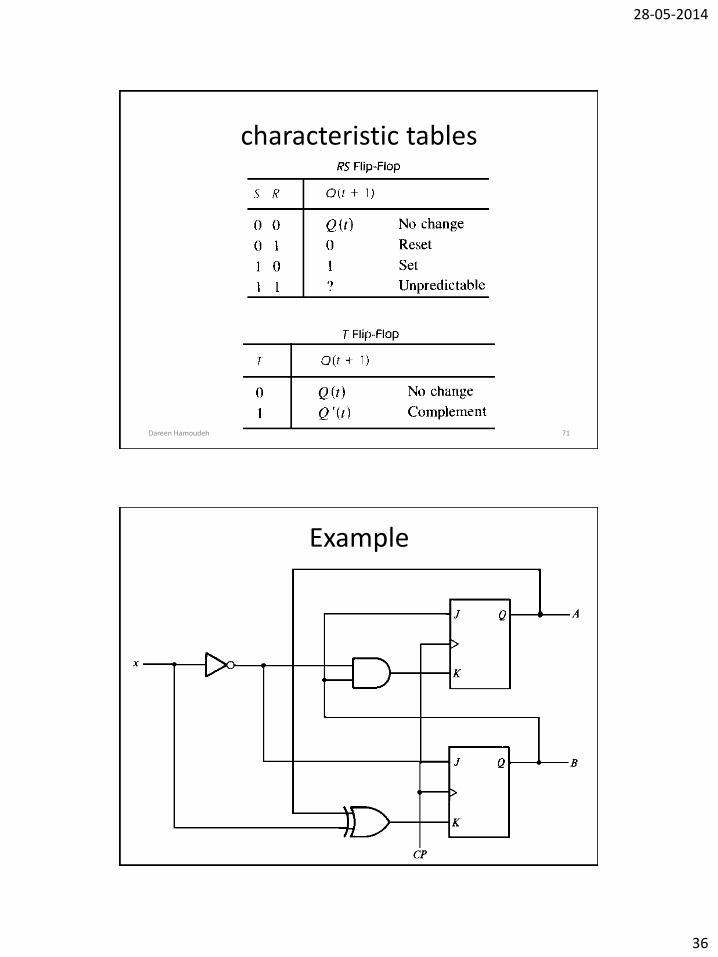
characteristic tables
Dareen Hamoudeh 70
28-05-2014
36
characteristic tables
Dareen Hamoudeh 71
Example
Dareen Hamoudeh 72
28-05-2014
37
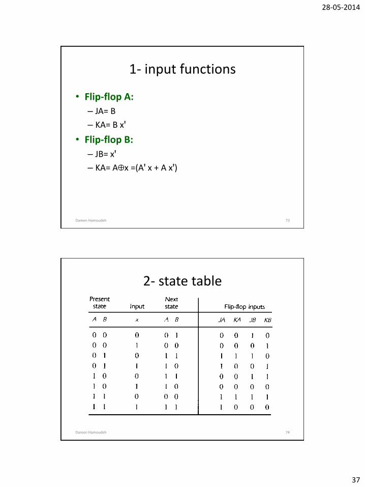
1- input functions
• Flip-flop A:
– JA= B
– KA= B xꞌ
• Flip-flop B:
– JB= xꞌ
– KA= A x =(Aꞌ x + A xꞌ)
Dareen Hamoudeh 73
2- state table
Dareen Hamoudeh 74
28-05-2014
38
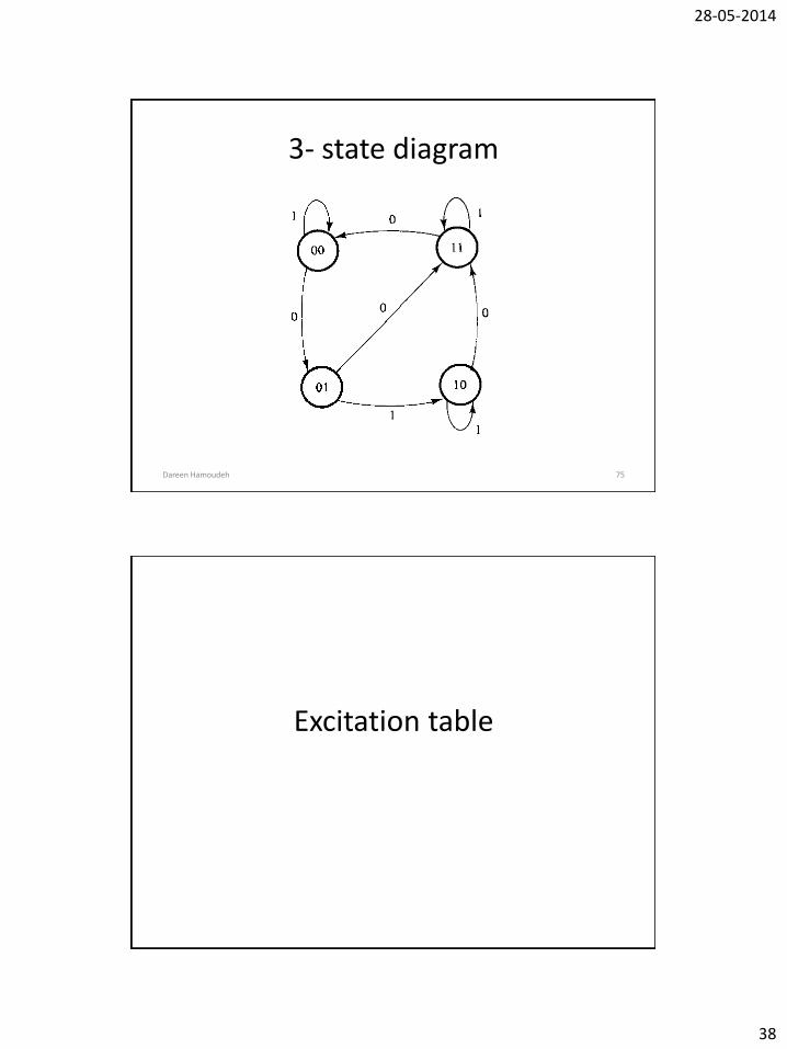
3- state diagram
Dareen Hamoudeh 75
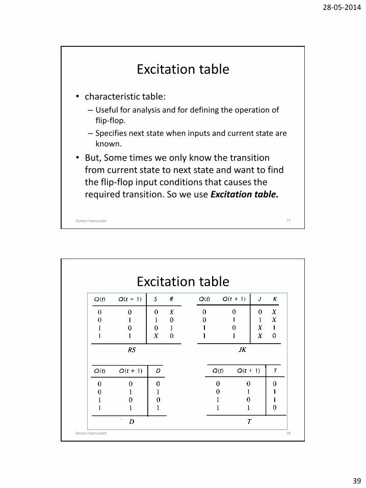
Excitation table
28-05-2014
39
Excitation table
• characteristic table:
– Useful for analysis and for defining the operation of flip-flop.
– Specifies next state when inputs and current state are known.
• But, Some times we only know the transition from current state to next state and want to find the flip-flop input conditions that causes the required transition. So we use Excitation table.
Dareen Hamoudeh 77
Excitation table
Dareen Hamoudeh 78