Chapter-7 X-ray and Electron Microscopy
36
Chapter VII: X-Ray and Electron Microscopy G. Springholz - Nanocharacterization I VII / 1 Chapter 7 X-Ray and Electron Microscopy Optical Elements, Lens Aberrations and Resolution Limits Chapter VII: X-Ray and Electron Microscopy G. Springholz - Nanocharacterization I VII / 2 Contents - Chapter 7 X-Ray and Electron Microscopy 7.1 Introduction ........................................................................................................................ 3 7.2 EUV & X-Ray Microscopy................................................................................................... 4 7.2.1 Extreme UV Optical Systems ............................................................................................................................... 5 7.2.2 X-Ray Optics ..................................................................................................................................................... 10 7.2.3 X-Ray Microscopy Set-Ups ................................................................................................................................ 15 7.3 Electron Microscopy ........................................................................................................ 20 7.3.1 Representatives of Electron Microscopy ............................................................................................................ 21 7.3.2 Basic Components............................................................................................................................................. 22 7.3.2 Comparison: SEM versus TEM .......................................................................................................................... 23 7.4.1 TEM Modes: Diffraction ..................................................................................................................................... 27 7.4.3 TEM Resolution ................................................................................................................................................. 30 7.4.4 Principle of Magnetic Electron Lenses ............................................................................................................... 31 7.4.5 Aberrations of Electron Lenses .......................................................................................................................... 33 7.4.6 Resolution due to Lens Aberrations and Diffraction ........................................................................................... 34 7.4.7 Ultra-High Resolution TEM with Sub-Ångström Resolution ................................................................................ 36 7.5 Scanning Electron Microscopy - SEM............................................................................. 38 7.5.1 Instrumentation .................................................................................................................................................. 39 7.5.2 Resolution Factors ............................................................................................................................................. 40 7.5.3 The Geometrical Spot Size and its Relation to the Probe Current ...................................................................... 41 7.5.4 Electron Spot Size due to Diffraction and Aberrations ........................................................................................ 45 7.5.5 Depth of Field and Depth of Focus.................................................................................................................... 52 7.5.6 SEM Imaging using Backscattered and Secondary Electron Emission .............................................................. 55 7.5.7 Spatial Distribution of Emitted Electrons ............................................................................................................ 57 7.5.8 Energy Distribution of Emitted Electrons and Energy Filtering .......................................................................... 62 7.5.9 SEM Resolution ................................................................................................................................................. 64 7.5.10 Contrast in SEM............................................................................................................................................... 66 7.6 Summary ........................................................................................................................... 72
Transcript of Chapter-7 X-ray and Electron Microscopy

Chapter VII: X-Ray and Electron Microscopy G. Springholz - Nanocharacterization I VII / 1
Chapter 7
X-Ray and Electron Microscopy Optical Elements, Lens Aberrations and Resolution Limits
Chapter VII: X-Ray and Electron Microscopy G. Springholz - Nanocharacterization I VII / 2
Contents - Chapter 7
X-Ray and Electron Microscopy 7.1 Introduction .................................. ...................................................................................... 3
7.2 EUV & X-Ray Microscopy ........................ ........................................................................... 4
7.2.1 Extreme UV Optical Systems ............................................................................................................................... 5
7.2.2 X-Ray Optics ..................................................................................................................................................... 10
7.2.3 X-Ray Microscopy Set-Ups ................................................................................................................................ 15
7.3 Electron Microscopy ........................... ............................................................................. 20
7.3.1 Representatives of Electron Microscopy ............................................................................................................ 21
7.3.2 Basic Components ............................................................................................................................................. 22
7.3.2 Comparison: SEM versus TEM .......................................................................................................................... 23
7.4.1 TEM Modes: Diffraction ..................................................................................................................................... 27
7.4.3 TEM Resolution ................................................................................................................................................. 30
7.4.4 Principle of Magnetic Electron Lenses ............................................................................................................... 31
7.4.5 Aberrations of Electron Lenses .......................................................................................................................... 33
7.4.6 Resolution due to Lens Aberrations and Diffraction ........................................................................................... 34
7.4.7 Ultra-High Resolution TEM with Sub-Ångström Resolution ................................................................................ 36
7.5 Scanning Electron Microscopy - SEM ............ ................................................................. 38
7.5.1 Instrumentation .................................................................................................................................................. 39
7.5.2 Resolution Factors ............................................................................................................................................. 40
7.5.3 The Geometrical Spot Size and its Relation to the Probe Current ...................................................................... 41
7.5.4 Electron Spot Size due to Diffraction and Aberrations ........................................................................................ 45
7.5.5 Depth of Field and Depth of Focus.................................................................................................................... 52
7.5.6 SEM Imaging using Backscattered and Secondary Electron Emission .............................................................. 55
7.5.7 Spatial Distribution of Emitted Electrons ............................................................................................................ 57
7.5.8 Energy Distribution of Emitted Electrons and Energy Filtering .......................................................................... 62
7.5.9 SEM Resolution ................................................................................................................................................. 64
7.5.10 Contrast in SEM ............................................................................................................................................... 66
7.6 Summary ....................................... .................................................................................... 72

Chapter VII: X-Ray and Electron Microscopy G. Springholz - Nanocharacterization I VII / 3
7.1 Introduction For optical light microscopy (see previous chapter) the best resolution is mainly given by the diffraction limit rdiff = 0.61 . λλλλ /NA due to nearly perfect, high numerical aperture and aberration free optical systems.
» Thus, the best resolution of light microscopy is about half of the wavelength, i.e., rbest ~ λλλλ /2 ~ 200nm
» Shorter imaging wavelengths are required to obtain higher spatial resolution: » EUV, X-rays or electrons.
X-rays: λλλλ ~ 1 Å ; rbest ~ 10 – 100 nm (= NA-limited because α = small)
Electrons: λλλλ ~ 0.1 – 0.01 Å ; rbest ~ 1 nm (= aberration-limited because of highly imperfect electron lenses)
For these short wavelength probes, however, no aberration free, high NA optical lenses exist .
Thus, in this case the resolution is mainly limited by the optics and not so much by the wavelength, i.e., the best achievable resolution is r >> λλλλ .
Other complications:
Normal refractive lenses do not work » alternative optical elements are required
Small wavelengths mean high particle/photon energies (~keV). This means » different interaction and contrast mechanisms are present.
The wavelength is comparable to interatomic distances » Diffraction at atomic lattices occur.
10-1 100 101 102 103 104 10510-4
10-3
10-2
10-1
100
101
102
103 IRvisible
UV
X-rays
He-ions
e-beam
Bea
m w
avel
engt
h (n
m)
Energy (eV)
Photons Electrons He-ions
α-particles
Chapter VII: X-Ray and Electron Microscopy G. Springholz - Nanocharacterization I VII / 4
7.2 EUV & X-Ray Microscopy To improve the resolution of optical microscopes, one could simply use EM radiation with shorter wavelength.
At short wavelengths, the photon energy increases beyond Ehv > 10 eV when λ < 120 nm. As a result, the light-matter interaction of the photons drastically changes.
Resulting Problems:
1. Optical materials are no longer transparent because absorption always occurs (hv > WA).
2. The refractive index of all materials approaches n = 1. Therefore, conventional refractive optics does not work in the UVU and XR regime, i.e. different optics are needed : Transition from refractive to reflective or diffractive optics !
3. Samples are no longer optically transparent. » EUV transmission microscopy possible only for very thin specimen. For reflection mode the reflectivity signal is small due to the small differences in the refractive indices of different materials (n ~1): R = [(n-1)/(n+1)]2
4. UV & VUV light is absorbed in air : Vacuum required for VUV systems (but not for x-rays)
5. No readily available, cost effective light sources are available » plasma sources/synchrotrons
6. Damaging of optics and samples by irradiation can occur due to high photon energies.

Chapter VII: X-Ray and Electron Microscopy G. Springholz - Nanocharacterization I VII / 5
7.2.1 Extreme UV Optical Systems #
All solids, liquids, and gasses absorb EUV photons : Thus, EUV light is already completely absorbed in 100 nm of H2O. As a result, reflective or diffractive optical elements are needed.
At short wavelengths, however, the refractive index of all materials approaches n ~ 1. Thus, for all materials also the reflectivity in the EUV is very small, i.e., R < 0.1 % !
Therefore, a high reflectivity can be obtained only by the reflection at many interfaces using
multilayer Bragg mirrors. Such multilayers are designed such that the waves reflected at each interface interfere constructively with each other, such that the reflectivities of all interfaces add up.
X-rays: δ ~ 10-4 – 10-6
R = [(n-1)/(n+1)]2
Chapter VII: X-Ray and Electron Microscopy G. Springholz - Nanocharacterization I VII / 6
Multilayer Bragg Mirrors
For EUV and soft X-ray optics, curved reflective Bragg mirrors consisting of many layers of e.g. molybdenum (high Z and high MA) and silicon (low Z and MA) with maximum refractive index contrast are employed.
Design: The individual layer thicknesses are designed such that the light reflected at each interface interferes constructively in backscattering geometry.
This means that the optical thickness of each layer should be equal to λλλλ/4 under normal incidence.
In the EUV where λ < 20nm this means that layer thicknesses well below 5 nm are needed.
Since for each single interface, the reflectivity is still very low R < 1%, many periods are required to obtain a large total reflectivity.
In this way, EUV Bragg mirrors can reflect nearly 70 % of EUV light at 13.5 nm when the number of multilayer periods (N>50) is large. Without coating, light would be almost totally absorbed.
The thicknesses and compositions of all films must controlled to better than 1 nm.

Chapter VII: X-Ray and Electron Microscopy G. Springholz - Nanocharacterization I VII / 7
Example: Mo/Si Bragg Mirror
Mo/Si multilayer with N = 40 layer pairs:
Yields ~70% reflectivity at 13.5nm where Mo and Si are most transparent.
For high reflection, the absorption should be low (i.e. attenuation length should be large). Mo, Si, Be are good candidates at λ∼10-15nm.
Chapter VII: X-Ray and Electron Microscopy G. Springholz - Nanocharacterization I VII / 8
In addition, the mirror surfaces have to be nearly perfectly flat with RMS roughness < 0.2 nm. Even small defects in coatings can strongly degrade the quality of the mirrors.
EUV systems are very expensive and therefore the main current application is not for microscopy but actually EUV-lithography for fabrication of IC Si chips with <20nm feature size.
Chapter VII: X-Ray and Electron Microscopy G. Springholz - Nanocharacterization I VII / 9
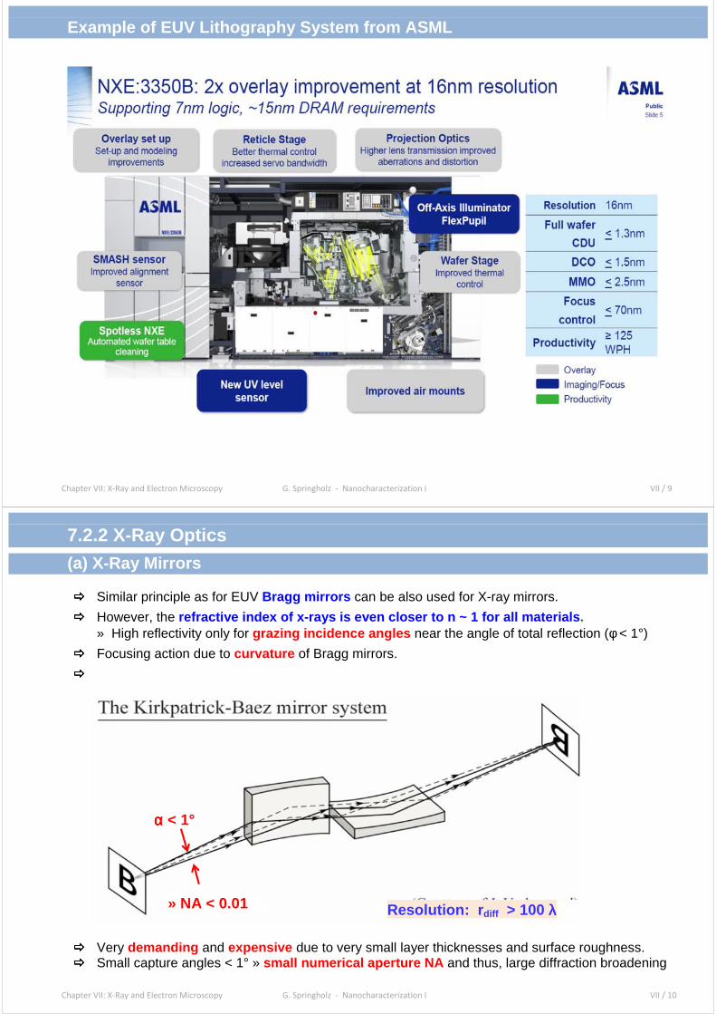
Example of EUV Lithography System from ASML
Chapter VII: X-Ray and Electron Microscopy G. Springholz - Nanocharacterization I VII / 10
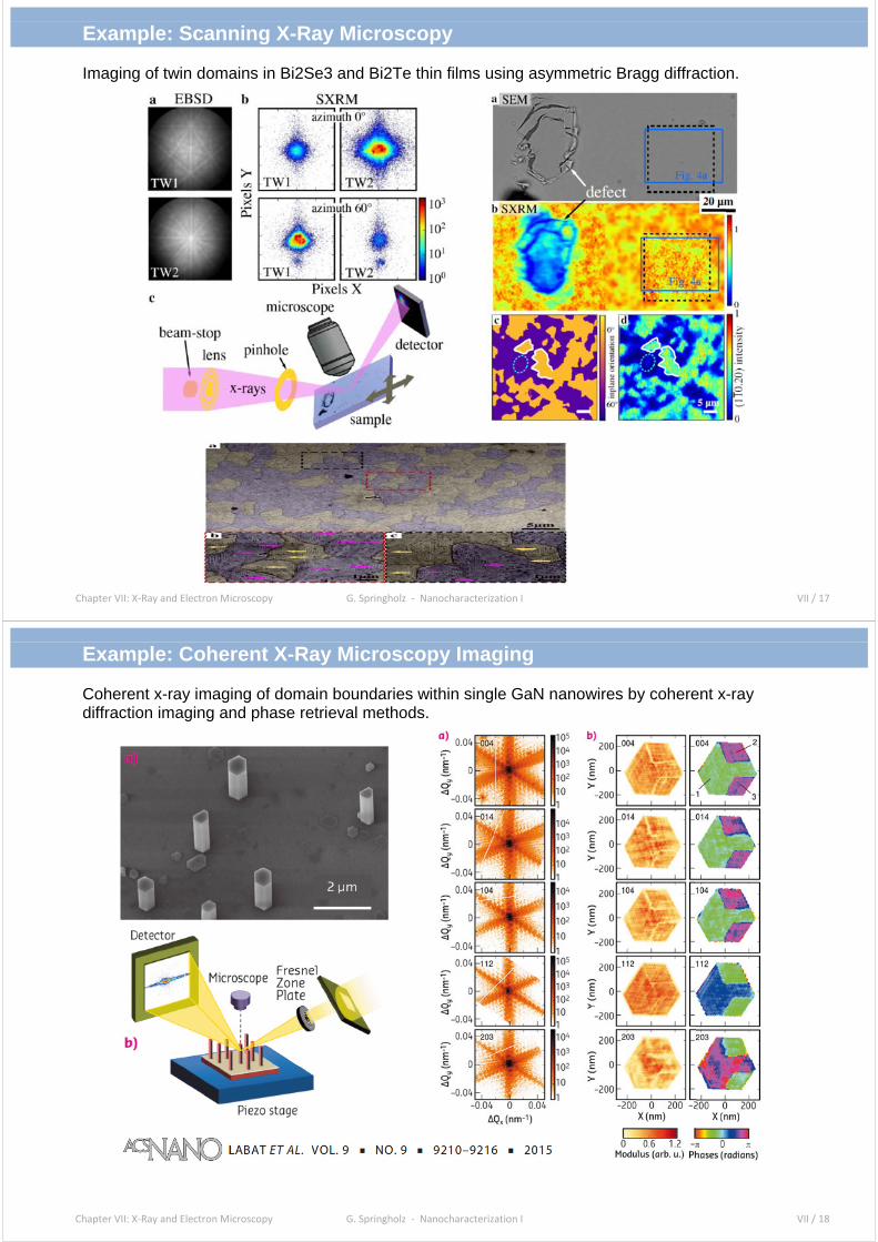
7.2.2 X-Ray Optics
(a) X-Ray Mirrors
Similar principle as for EUV Bragg mirrors can be also used for X-ray mirrors.
However, the refractive index of x-rays is even closer to n ~ 1 for all materials . » High reflectivity only for grazing incidence angles near the angle of total reflection (φ < 1°)
Focusing action due to curvature of Bragg mirrors.
Very demanding and expensive due to very small layer thicknesses and surface roughness. Small capture angles < 1° » small numerical aperture NA and thus, large diffraction broadening
αααα < 1°
» NA < 0.01 Resolution: rdiff > 100 λλλλ

Chapter VII: X-Ray and Electron Microscopy G. Springholz - Nanocharacterization I VII / 11
(b) Diffractive Optics: Fresnel Zone Plates
Focusing optical elements can be also made based on diffraction.
These elements are called Fresnel zone plates and consist of diffraction gratings with graded line spacing ∆∆∆∆r that decreases with increasing radius r from the optical axis.
Fresnel zone plate
Chapter VII: X-Ray and Electron Microscopy G. Springholz - Nanocharacterization I VII / 12
SEM Images of X-Ray Fresnel Zone Plate

Chapter VII: X-Ray and Electron Microscopy G. Springholz - Nanocharacterization I VII / 13
Numerical Aperture
λ (~0.1 – 1 nm) << 2∆r (>20nm) » NA << 0.05 !!
Diffraction limited resolution : r = 0.66 λ / NA » r ~ 50 nm
=last ring spacing
Example: N = 100, λ = 1Å, ∆r = 20nm » f = 1.64 mm
Chapter VII: X-Ray and Electron Microscopy G. Springholz - Nanocharacterization I VII / 14
Achievable Microscopy Resolution
Resolution determined by smallest outer ring spacing ∆r of Fresnel lens (determined by fabrication process)
Actual resolution worse due to lens imperfections

Chapter VII: X-Ray and Electron Microscopy G. Springholz - Nanocharacterization I VII / 15
7.2.3 X-Ray Microscopy Set-Ups
The most simplest and common approach is to use scanning microscopy , where a finely focused x-ray beam with a spot size of down to few 10 nm is scanned over a sample. Due to the small numerical aperture of x-ray focusing elements, the spot size and resolution is > 100 λλλλ.
Chapter VII: X-Ray and Electron Microscopy G. Springholz - Nanocharacterization I VII / 16
Chapter VII: X-Ray and Electron Microscopy G. Springholz - Nanocharacterization I VII / 17
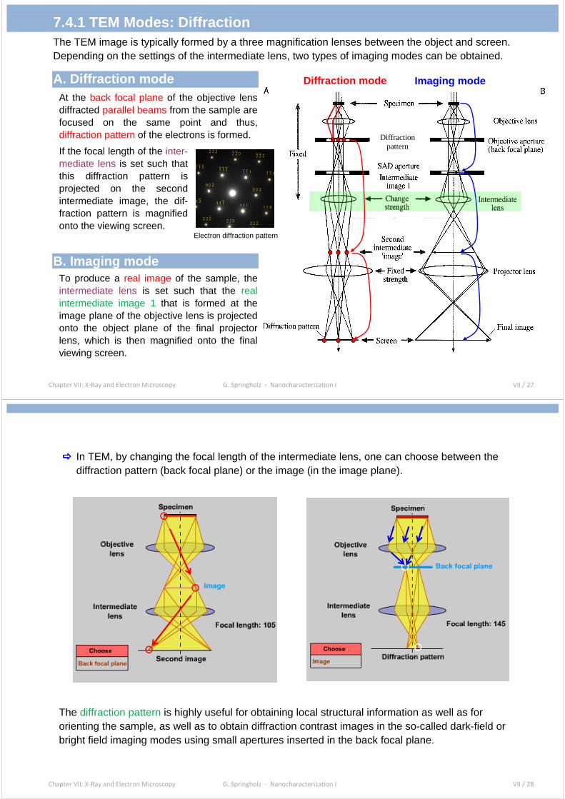
Example: Scanning X-Ray Microscopy
Imaging of twin domains in Bi2Se3 and Bi2Te thin films using asymmetric Bragg diffraction.
Chapter VII: X-Ray and Electron Microscopy G. Springholz - Nanocharacterization I VII / 18
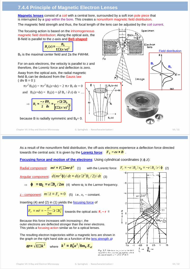
Example: Coherent X-Ray Microscopy Imaging
Coherent x-ray imaging of domain boundaries within single GaN nanowires by coherent x-ray diffraction imaging and phase retrieval methods.

Chapter VII: X-Ray and Electron Microscopy G. Springholz - Nanocharacterization I VII / 19
Further Examples
Resolution (= x-ray spot size) down to about 12 nm have been demonstrated !
Chapter VII: X-Ray and Electron Microscopy G. Springholz - Nanocharacterization I VII / 20
7.3 Electron Microscopy
Electrons microscopes provide a very high spatial resolution down to ~ nm due to the orders of magnitude shorter wavelength of electron beams compared to visible light.
This drastically reduces the diffraction limit.
De Broglie wavelength of electrons : (E < 100keV)
compare photon wavelength: (E ~ 1-3eV)
Relativistic electrons: λrel = h / [2 m0,e. E (1+E/2 m0,e
.c2 )]1/2 (E > 100kV).
For electron energies E > 150 eV the electron wavelength is λ <1 Å ! This also applies to protons or ion beams where λ << 1 Å already for E >1eV.
Scanning electron microscope – SEM: E ~ 2 – 50 keV, Transmission electron microscope – TEM: E ~ 50 – 300 keV
[ ]eVEnmcphoton 1240 =υ=λ
)(225.1 eVEnmmv
helectron ==λ
αλ sin61.0 nrdiff ⋅=

Chapter VII: X-Ray and Electron Microscopy G. Springholz - Nanocharacterization I VII / 21
7.3.1 Representatives of Electron Microscopy
(1) Transmission Electron Microscopy (TEM) (~100 – 300 keV, typical) Imaging using electron waves transmitted through thin sample slices using magnification optics.
= Analogon to optical imaging microscopy and thus, follows same principles and properties.
Features: Highest spatial resolution (~Å) and strong diffraction contrast because the electron wavelength is comparable or smaller compared to the interatomic lattice spacings. This results in very high sensitivity to structural properties, such as lattice defects, crystal structure and orientation, etc.
However: Electron transparent specimen required: Thickness less than about <100 nm.
(2) Scanning Electron Microscopy (SEM and STEM) (SEM: 2 - 50 keV. STEM: 10 – 200keV) Imaging using a focused electron beam that is raster scanned across the sample.
SEM: Recording of the excited secondary and backscattered electrons. Imaging from above.
STEM: Recording of transmitted electrons or induced secondary electrons ejected during transmission of thin sample specimen (STEM = scanning transmission electron microscope).
Features: High sensitivity to surface morphology, large range of magnifications, large depth of focus. Versatile and easy to use: No sample preparation needed (except for biological specimen).
(3) Low-Energy Electron Microscopy (LEEM) (~10 eV – 1000 eV) Imaging using electron waves reflected from the samples. Features: High surface sensitivity due to very low penetration depth of low energy electrons of <1nm. Many imaging and spectroscopy modes.
(4) Photo Electron Emission Microscopy (PEEM) (eV to 500 eV) Imaging using photoelectrons emitted due to illumination with UV or X-ray light. Features: High surface sensitivity due to small escape depth. Electronic structure.
PEEM
Chapter VII: X-Ray and Electron Microscopy G. Springholz - Nanocharacterization I VII / 22
7.3.2 Basic Components
Electron microscopes consist of following component s:
•••• Electron source : Electron gun
and high voltage sources
•••• Electro-optical column with electron optics (magnetic or electrostatic lenses, beam deflection, apertures, ..)
•••• Sample chamber with movable and tiltable sample stage
•••• Electron detectors + optional x-ray detectors for chemical analysis
•••• High vacuum system: HV pumps, valves pressure gauges, …
•••• Load lock chamber for rapid sample exchange
•••• Control electronics & computer control system
•••• Image analysis and processing software
•••• Sample preparation : TEM: Thinning / cutting / polishing SEM: Conductive coating (Au, graphite , …)

Chapter VII: X-Ray and Electron Microscopy G. Springholz - Nanocharacterization I VII / 23
7.3.2 Comparison: SEM versus TEM
SEM TEM
SEM set up and features:
Demagnifying optics to produce small spot size. Detection of secondary / backscattered electrons. Sensitive to surface morphology and composition. Large sample sizes and thicknesses possible. Best resolution at intermediate/low e- energy.
TEM set-up and features:
Magnifying optics to produce enlarged image. Detection of transmitted electrons & waves. Strong diffraction effects, sensitive to structure. Electron-transparent thin sample slices required. Resolution increases with higher e- energy.
Chapter VII: X-Ray and Electron Microscopy G. Springholz - Nanocharacterization I VII / 24
Optical Diagram for TEM
TEM is the electron analog to an optical microscope, in which by magnification lenses a highly enlarged real image of the sample is produced on a viewing screen, in which the contrast reflects the probability that an electron impinging on a given spot on the sample reaches the detector.
Magnification in each stage: ββββi ~ ββββi / fi, from lens equation (see chapter 5) Magnetic electron lenses: Focal length fi can be varied continuously by changing the magnetic field strength. Total magnification ββββtot = ββββ1 x ββββ2 x ββββ3
image #1
image #2
ββββ1= b1/f1
ββββ2= b2/f2
Electron gun
sample
sample
objective lens
intermediate lens
image #2
projection lens
final image
ββββ3= b3/f3
Electron gun

Chapter VII: X-Ray and Electron Microscopy G. Springholz - Nanocharacterization I VII / 25
Features of TEM
•••• TEMs are usually operated at high voltages ~ 50 -300keV to obtain the highest resolution and long transmission lengths. This requires considerably expensive high voltage components.
•••• The electo-optical column consist of a separate collimation and magnification lens systems.
•••• 2D detectors for image recording such a fluorescent screens or CCD cameras.
•••• Different imaging modes available that require additional apertures in the optical path.
•••• Transmission requires thin sample specimens: Difficult sample preparation.
Chapter VII: X-Ray and Electron Microscopy G. Springholz - Nanocharacterization I VII / 26
Special features of TEM
1. The image contrast can be drastically changed using different apertures and imaging modes: Bright-field, dark-field, phase contrast, high-resolution mode, etc. ..
2. For TEM imaging, the sample specimen have to be thinned to few 100 nm or below to become electron transparent. Thinner samples yield higher spatial resolution. This requires special sample preparation techniques.
3. Higher resolution is achieved down to 0.1 nm. This is mainly due to the higher electron energy as well as reduced electron sample scattering due to the thin sample thickness.
4. Apart from imaging, also local electron microdiffraction investigation can be performed for structure analysis.
5. Energy filtering as well as electron energy loss spectroscopy (EELS) can be applied to obtain chemical contrast images.
6. Apart from parallel imaging, TEM can be also operated in a scanning transmission electron microscopy mode (STEM), where the electron beam is tightly focused and scanned across the sample like in a SEM. The transmitted, scattered or induced secondary electrons can be detected by additional detectors positioned close to the sample.
High resolution TEM
diffraction Cu grains
Red=O, Green=N, Blue=Si
EELS imaging of MOS transitor
Chapter VII: X-Ray and Electron Microscopy G. Springholz - Nanocharacterization I VII / 27
7.4.1 TEM Modes: Diffraction The TEM image is typically formed by a three magnification lenses between the object and screen. Depending on the settings of the intermediate lens, two types of imaging modes can be obtained.
A. Diffraction mode At the back focal plane of the objective lens diffracted parallel beams from the sample are focused on the same point and thus, diffraction pattern of the electrons is formed.
If the focal length of the inter-mediate lens is set such that this diffraction pattern is projected on the second intermediate image, the dif-fraction pattern is magnified onto the viewing screen.
B. Imaging mode To produce a real image of the sample, the intermediate lens is set such that the real intermediate image 1 that is formed at the image plane of the objective lens is projected onto the object plane of the final projector lens, which is then magnified onto the final viewing screen.
Diffraction mode Imaging mode
Diffraction pattern
Electron diffraction pattern
Chapter VII: X-Ray and Electron Microscopy G. Springholz - Nanocharacterization I VII / 28
In TEM, by changing the focal length of the intermediate lens, one can choose between the
diffraction pattern (back focal plane) or the image (in the image plane).
The diffraction pattern is highly useful for obtaining local structural information as well as for orienting the sample, as well as to obtain diffraction contrast images in the so-called dark-field or bright field imaging modes using small apertures inserted in the back focal plane.

Chapter VII: X-Ray and Electron Microscopy G. Springholz - Nanocharacterization I VII / 29
Example:
Diffraction contrast in the bright field mode for a thin Ti- foil: Make dislocations and crystal defects visible in the selected sample area.
Chapter VII: X-Ray and Electron Microscopy G. Springholz - Nanocharacterization I VII / 30
7.4.3 TEM Resolution
Because the aberrations of electron lenses are very larger, i.e., raber > rdiff the practical resolution of is mostly limited by lens aberrations.
Electron Lenses Electrons can be deflected by electric or magnetic fields, but magnetic fields are generally more effective at high electron energies because the Lorentz force increases with electron velocity.
For a focusing action, a nonuniform radially varying B-field distribution is required such that outer electrons are bend more strongly towards the optical axis than near-axis electrons.
Such a nonuniform magnetic field is produced by the stray field of a coil surrounded by a iron pole piece that is interrupted by a gap in the central bore.
Since the field strength can be changed through the applied voltage or current, the focal length of electron lenses can be continuously adjusted.
Aberrations : Due to the non-ideal magnetic field distribution, electron lenses exhibit very large intrinsic lens aberrations.
Due to these aberrations, the aperture angles of electron lenses must be kept very small, in order to limit the effect of lens errors, which rapidly increases with αn . Typically α ≤ 0.3° !
⇒⇒⇒⇒ Achievable NA is much smaller than for optical lenses: NATEM ~ 0.005 ⇒⇒⇒⇒ reff ~ 100 λλλλ
BveFL
rrr××××⋅⋅⋅⋅====
reff = (r2dif
+ r2aber)
1/2
Chapter VII: X-Ray and Electron Microscopy G. Springholz - Nanocharacterization I VII / 31
7.4.4 Principle of Magnetic Electron Lenses
Magnetic lenses consist of a coil with a central bore, surrounded by a soft iron pole piece that is interrupted by a gap within the bore. This creates a nonuniform magnetic field distribution.
The magnetic field strength and thus, the focal length of the lens can be adjusted by the coil current.
The focusing action is based on the inhomogeneous magnetic field distribution: Along the optical axis, the B-field is parallel to the z-axis and Bell-shaped :
B0 is the maximal center field and 2a the FWHM.
For on-axis electrons, the velocity is parallel to z and therefore, the Lorentz force and deflection is zero.
Away from the optical axis, the radial magnetic field Br can be deduced from the Gauss law ( div B = 0 ):
π r2 Bz(z) − π r2 Bz(z+dz) − 2 π r Br dz = 0
and Bz(z+dz) = Bz(z) + (∂ Bz / ∂ z) dz + …
⇒
because B is radially symmetric and Bϕ= 0.
20
)/(1)(
az
BzBz ++++
====
[[[[ ]]]]22
0
)/(12 az
Bzr
z
BrB z
r++++
⋅⋅⋅⋅⋅⋅⋅⋅====∂∂∂∂
∂∂∂∂−−−−≈≈≈≈
Field distribution
Bz
Br
Chapter VII: X-Ray and Electron Microscopy G. Springholz - Nanocharacterization I VII / 32
As a result of the nonuniform field distribution, the off-axis electrons experience a deflection force directed towards the central axis: It is given by the Lorentz force : BevFL ××××−−−− .
Focusing force and motion of the electrons : Using cylindrical coordinates (r,ϕ,z):
Radial component: 2ϕ&&& mrFrm r ++++==== (1) with the Lorentz force: ϕ⋅⋅⋅−=⋅⋅−= ϕ &rBevBeF zzr (2)
Angular component: dtBreddtmrd z /)2/(/)( 22 ⋅=ϕ& (3)
⇒ mBe zL 2/⋅⋅⋅⋅====ωωωω====ϕϕϕϕ& (4) where ωL is the Larmor frequency.
z - component: 0≈=⋅ zFzm && (5) i.e., vz ~ constant. Inserting (4) and (2) in (1) yields the focusing force of
22
2 zr Brm
ermF ⋅⋅−== && towards the optical axis: Fr ~ r !!
Because this force increases with increasing r, the outer electrons are deflected stronger than the inner electrons. This yields a focusing action similar as for a optical lenses. The resulting electron trajectories within a magnetic lens are shown in the graph on the right hand side as a function of the lens strength ω:
21 k++++====ωωωω where elEmaBk 0
220
2 8====

Chapter VII: X-Ray and Electron Microscopy G. Springholz - Nanocharacterization I VII / 33
7.4.5 Aberrations of Electron Lenses
The focal points of electrons incident at different distance from the optical axis r are not on the same point. Magnetic lenses therefore exhibit rather large lens aberrations:
(i) Spherical Aberration: (Parallel beams are not focused exactly on the same focal point).
» Broadening of the spot size rsph in the focal plane. Increases with α:
» Spherical aberration constant are typically Cs ~ mm for TEM lenses, increases with increasing lens strength proportional to the focal length.
Example : For Cs = 3mm => (i) α = 1° (12 mrad) → rsph = 5 nm ; (ii) α = 5° (87 mrad) → rsph = 2 µm
(ii) Chromatic Aberration:
(Slower electrons are bend more strongly than faster electrons) » Resulting broadening of the spot size (spot radius rchr) is given by:
» Chromatic aberration constant Cc ~ mm , increases with decreasing lens strength.
Although the energy spread of the primary electrons is typically smaller than 2 eV, the energy spread ∆E of the electrons transmitted through the sample is much larger (15 – 25 eV) due to inelastic scattering. ∆E increases with increasing sample thickness, i.e., chromatic errors increase.
(ii) Astigmatism: When the pole pieces are not perfectly symmetric and the optical axis not perfectly aligned, the electrons experience a non-uniform not radially symmetric magnetic field:
Scherzer Theorem : Aberrations are intrinsic for rotational symmetric magnetic lenses and can in principle only be corrected by use of complicated multipole lenses.
3αssph Cr =
α0EE
Cr cchr∆=
frast ∆= α
Chapter VII: X-Ray and Electron Microscopy G. Springholz - Nanocharacterization I VII / 34
7.4.6 Resolution due to Lens Aberrations and Diffra ction For any nonperfect lens system, the resolution is limited by
(i) diffraction where rdiff ~ 1/sinα , as well as by (ii) lens aberrations where raber ~ αn ,
Total effective resolution is given by: r tot = (rdiff2 + rshp
2 + rchr2 + rast
2 )1/2
Using sinα ≈ α, this yields: r tot = [ (0.61 . λλλλ /αααα)2 + (Csph.αααα3 3 3 3 )2 + (Cchr
.∆∆∆∆E/E . αααα)2 ]1/2 α = aperture angle. Csph and Cchr = spherical and chromatic lens aberration constants.
With increasing aperture αααα the diffraction broadening decreases but the broadening due to the lens aberration increases.
When the lens aberrations cannot be neglected, there exists a certain optimum aperture angle ααααopt where the highest resolution is achieved !
This applies to all microscopy methods.
Figure: Resolution of an electron microscope as a function of aperture angle due to (i) diffraction, (ii) spherical aberration, and (iii) chromatic aberration. Calculated for E =300 keV, ∆Eunfiltered= 250 eV, ∆Efiltered= 30eV, Cs = 3.2 mm, Cc = 3.0 mm, and fobj = 3.9 mm.
αλ⋅= sin61.0 nrdiff
Resolution factors versus aperture angle
rdiff ~ αααα-1
rsph~ αααα3
rchr~ αααα1
Resolution factors versus aperture angle
ααααopt

Chapter VII: X-Ray and Electron Microscopy G. Springholz - Nanocharacterization I VII / 35
TEM Resolution
plotted as a function of:
• aperture angle α, • spherical aberration C • electron energy E
Maximum (best) resolution (w/no Cchr)
= Minimum of rtot neglecting chromatic & astigmatic aberrations
drtot/dαααα = 0 → αopt = 0.77 mrad . (λ / Csph)1/4 and rbest = 0.91 . (Csph
. λλλλ3 )1/4 at α= αopt
Example: 200 keV, λ = 0.0274 Å, Csph = 0.5 mm: » αopt = 6.6 mrad = 0.38° » rbest = 2.9 Å
With chromatic aberration: Cchr = 2 mm & ∆E = 20eV@200 keV: At αopt = 6.6 mrad » reff = 13.5 Å
Chromatic aberration broadening is minimized when (i) using higher electron energies (smaller ∆E/E) and (ii) for thin as possible specimens. This is essential for high resolution !
From Bethe equation: dE/dx = 1… 3 eV per nm for 100 keV electrons (depending on material) !
0,1 11
10
100
1000
TEM Resolution
+Cc=2/∆E=20eVCs=0.05
Cs=0.5
Cs=5
50kV
200kV
Res
olut
ion
(A)
Aperture angle (deg)
800kV
222chrsphrdifftot rrrr ++=
Chapter VII: X-Ray and Electron Microscopy G. Springholz - Nanocharacterization I VII / 36
7.4.7 Ultra-High Resolution TEM with Sub-Ångström R esolution TEM Resolution is mainly limited spherical aberration: rmin = 0.91 . (Csph
. λλλλ3 )1/4 » Resolution can be improved only by (a) decreasing the wavelength (=MeV TEMs) and/or
(b) and/or improveming the lens optics (aberration corrections).
Aberration corrections:
Scherzer (1936): Spherical aberrations cannot be avoided using rotationally symmetric fields ! Rose (1990ies): Spherical aberration corrections possible by using multipole fields that produce negative
third order spherical aberrations for compensation.
» Development of hexapole and octopole correction lenses that can reduce Csph to almost zero.
Additional measures for HR-TEM:
• Introduction of energy filters in the condenser system to improve the monochromaticity of the electron beam and thus reduce chromatic aberrations.
• Post sample energy filter (Omega filter
• Improved mechanical construction to reduce vibrations and thermal drifts of the TEM column.
• Improved stability and reduction of noise level of lens and gun currents.

Chapter VII: X-Ray and Electron Microscopy G. Springholz - Nanocharacterization I VII / 37
Resolution of Aberration Corrected TEM with Multipole Correction Lenses
0.0001
0.001
0.01
0.1
1
1800 1840 1880 1920 1960 2000 2040
Resolution (Ang.
-1 )
Year
Electron Microscope
Light Microscope
Corrected EM
Ross
Amici
Abbe
Ruska
Marton
Dietrich(200keV)
Haider(200keV)
C.L. Jia, M. Lentzen and K. Urban, Science 299, 870 (2003).
Sub-Ångstrom resolution can be achieved by modern aberration corrected ultra-high resolution TEMs !
aberration corrected TEM
Multipole Correctio n Lenses yields Cs values as low as µm
Chapter VII: X-Ray and Electron Microscopy G. Springholz - Nanocharacterization I VII / 38
7.5 Scanning Electron Microscopy - SEM
• In SEM, the sample is raster scanned with a sharply focused electron beam of a few nm diameter and energy of 5 - 50 keV. The magnification M is the ratio between scan size /display size .
• SEM images = Lateral intensity distribution of backward emitted secondary electrons or of the backscattered electrons recorded as a function of the beam position on the sample. Alternatively, the excited x-ray photons, luminescence or sample current images can be recorded.
Features : High resolution (~few nm), no sample preparation needed, chemical analysis & spectroscopy
Resolution depends on probe size and interaction volume. Trend towards lower electron energies.
Contrast depends on the interaction mechanisms, beam parameters and detection schemes.
sample
SE
electrons (1-30kV)
detector spectrometer
Display of I(x,y)
scanning
detector
image processor data storage
I(t)
BSE
hνννν x-rays
photons
I(t) A
Scan generator
x,y(t)

Chapter VII: X-Ray and Electron Microscopy G. Springholz - Nanocharacterization I VII / 39
7.5.1 Instrumentation
viewing screen
control electronics
electron column
load lock sample manipulation
vacu
um tu
be
viewing screens
control electronics
electron column
load lock sample manipulation
Vaccum pumps
Detectors Sample
Chamber
electron gun
Vacuum tubes and high voltage connection
EDX
LN2
Chapter VII: X-Ray and Electron Microscopy G. Springholz - Nanocharacterization I VII / 40
7.5.2 Resolution Factors
In SEM, the lateral resolution is determined by three main factors:
1. The diameter of the focused electron beam spot size dprobe on the sample, given by:
It is determined by the combination of the geometrical spot size dgeom as well as the diffraction and abberation broadening ddiff and daberr . These depend on the beam current, aperture angle, lens aberrations, electron energy and wavelength, gun brightness, …..
Note: The minimal probe size represents the ultimate resolution limit of SEM !
2. The size of the interaction volume from which secondary electrons and other signal are generated. The interaction volume increases with increasing electron energy and decreasing mass density and Z number of the sample material.
3. Signal-to-noise noise ratio (~probe current), sample contrast, detection mode and efficiency , type of detector and energy filtering of secondary signals.
⇒ Points #2 and #3 define the practical resolution limit.
222abberationndiffractiolgeometricaprobe dddd ++++++++====

Chapter VII: X-Ray and Electron Microscopy G. Springholz - Nanocharacterization I VII / 41
7.5.3 The Geometrical Spot Size and its Relation to the Probe Current
The SEM lens system produces a small electron spot size with diameter dprobe on the sample surface by demagnification of the initial beam diameter d0 at the cross-over within the gun onto the sample using a multiple electron lens system. Thereby, the beam is reduced to a very small size.
Demagnification M = dimage / dobject << 1 .
For one lens: M = dim / dob = Lim / Lob = αout / αin ≈ f / L
ααααeff
d0,αααα0
Demagnification Optics
ααααp
Electron gun (thermionic)
Chapter VII: X-Ray and Electron Microscopy G. Springholz - Nanocharacterization I VII / 42
Resulting geometrical spot size dgeom for a three-lens system:
dgeom = m1 .m2
.m3 .d0 = Mtot
. d0 ≈ f1 f2
f3 / (L1
L2 L3)
. d0 where d0 is the initial crossover size of the electron gun.
Thermionic guns: d0= 50–100 µm, field emitters: d0~10 nm
Typical demagnifications : M = 1/50000… 1/10.
Resulting Probe Current Iprobe
Due to the final aperture ααααp, actually only a small part of the initial electron emission cone is projected onto the sample. This strongly reduces the probe current Iprobe.
The actual effective emission cone αeff of electrons emitted from the source focused onto the sample is given by:
αeff = m1.m2
.m3 . αp
Thus: αeff = M . αp
dgeom = M . d0
Example: Typical working distance WD = 10 mm (~ f3) and typical objective diaphragm diameter: 50 … 100 µm. Final aperture: αp = 5 - 10 mrad (0.2°) yields effective source aperture: αeff ~ 10-4 mrad !!
ααααeff
d0,αααα0
Demagnification Optics
ααααp ααααeff
Reducing the magnification M to achieve a small spot size simultaneously decreases the probe current !

Chapter VII: X-Ray and Electron Microscopy G. Springholz - Nanocharacterization I VII / 43
Relation between probe current, final aperture and geom etrical spot size
As shown above, the final aperture limits the beam current Ip in the final probe spot dgeom on the sample because only a reduced cone of emitted electrons with αeff < α0 is focused onto the sample.
The total emission current I0 emitted from the electron gun is given by:
)4/()( 20
20000 dAjI π⋅βαπ===
using the gun parameters
d0 = crossover diameter and brightness
The actual probe current Ip is then given by:
220
24
120
20
20
200 )/(4/)/( effeffeffp ddII αβπ=αα⋅π⋅βαπ=αα⋅=
Using αeff / α0 = M and M = dgeom / d0 yields the relation:
222
41222
02
41
pgeompp dMdI αβπαβπ ⋅⋅=⋅=
Thus, the geometrical spot size and the probe current are interrelated !
Conclusions:
For a given gun brightness β and final aperture αp, the reduction of the probe diameter dgeom by increasing the demagnification comes at the cost of reducing the beam current Ip !
An infinitely small geometrical beam spot is achieved only with an infinitesimal small probe current !
For a required probe beam current Ip, the smallest
achievable geometrical spot size dgeom is given by:
ααααeff
200 πα=Ω=β jAI ee
ppgeom Id ⋅πα⋅β= /4
12
4/4 −α⋅βπ
=⋅πα
β= p
pp
pgeom
IId
Chapter VII: X-Ray and Electron Microscopy G. Springholz - Nanocharacterization I VII / 44
Influence of the used Electron Guns
From the derived relation: follows: +
Thus, for a gun with higher brightness b, a much higher beam current can be obtained for a fixed geometrical spot size !
As a result, SEMs equipped with field emission or Schottky LaB6 guns usually provide a higher microscope performance with higher spatial resolution.
12
4/4 −α⋅βπ
=⋅πα
β= p
pp
pgeom
IId 2
22
4geom
pp dI ⋅β⋅
απ=

Chapter VII: X-Ray and Electron Microscopy G. Springholz - Nanocharacterization I VII / 45
7.5.4 Electron Spot Size due to Diffraction and Abe rrations
Neglecting all other factors, the ultimate SEM resolution is given by the electron spot size dprobe, which is larger than the geometrical spot size dgeom due to diffraction and lens aberrations.
The real final spot size dprobe is given by the root mean square sum of all broadening factors :
2222chrsphdiffgeomprobe ddddd ++++++++++++====
where: (see Chapter 5)
dgeom is the geometrical spot size, given by: dgeom = (4Ip / βπ2)1/2/ αp
ddiff is the diffraction broadening, given by: ddiff = 0.61 λ / αp
dshp is the spot broadening due to spherical aberration: dsph = Csph . αp
3 / 2
dchr is the spot broadening due to chromatic aberration: dchr = Cchr . ∆E/E. αp
Other lens aberrations are less important.
These factors depend on : Objective aperture ααααp, Electron energy E, Gun brightness ββββ , Probe current Ip and Lens properties (aberrations). Inserting the above relations yields:
22
62
22
22
211
)61.0(4
pchrpsphp
pprobe C
EE
CI
d αααα
∆∆∆∆++++αααα
++++αααα
λλλλ⋅⋅⋅⋅++++
βπβπβπβπ====
For small αp, the probe diameter is inversely proportional to αp , i.e., dprobe ~ 1 / αp
For large αp, the probe diameter increases proportional to αp3, i.e., dprobe ~ αp
3 .
Thus, for a given value of the probe current Ιp, gun brightness β and aberration constants Cshp,chf , there exists a certain optimum aperture ααααp,opt at which the spot size dprobe is minimized.
(see Chapter 4)
Chapter VII: X-Ray and Electron Microscopy G. Springholz - Nanocharacterization I VII / 46
(1) Dependence of the Spot Size dProbe on Aperture Angle ααααp
Cases: (a) ααααp and Ip small: dp is diffraction limited, i.e.: dp ~ 1 / α p
(b) ααααp small + I p large: dp is limited by current Ip ( dgeom): dp ~ 1 / αp
(c) ααααp large: dp is limited by spherical aberration: dp ~ αp3
(d) ααααp intermediate: dp is limited by chromatic aberration: dp ~ αp
22
62
22
22
21
1)61.0(
4
pchr
psph
p
pprobe
CEE
C
Id
αααα
∆∆∆∆++++
αααα
++++
αααα
λλλλ⋅⋅⋅⋅++++
βπβπβπβπ====
Plots: dprobe as a function of ααααp
FE gun:
Thermionic gun:
ddiff
dchr
dsph
dgeom ddiff
ddiff
dchr
FE gun & in-lens

Chapter VII: X-Ray and Electron Microscopy G. Springholz - Nanocharacterization I VII / 47
(2) Dependence of dprobe on Beam Current Ip
Thus: ConstI
d p
p
probe ++++βββββπαβπαβπαβπα
==== 2
Smaller spot sizes dp are obtained for small beam currents Ip and brighter electron guns (FE, LaB6 - large β) !
dprobe as a function of I p
ββββW / ββββFE ~ 103-4
Beam Spot Size
FE gun & in-lens
ddiff
dchr
dsph
dgeom
ddiff
ddiff
dchr
Thermionic gun
22
62
22
22
21
38.04
pchrpsph
p
pprobe C
EECI
d αααα
∆∆∆∆++++αααα
++++
αααα
λλλλ++++
βπβπβπβπ====
Smaller spot sizes dp for high brightness field emitter or LaB6 electron guns !
Chapter VII: X-Ray and Electron Microscopy G. Springholz - Nanocharacterization I VII / 48
(3) Dependence of dprobe on Beam Energy
with
Thus, for constant current Ip and fixed aperture αp :
ECCd constprobe 1~ 2++++
Consequence:
The probe size dp decreases with increasing electron energy E, at which also the gun brightness β increases !
o Small ααααp: dp limited by diffraction: 22 12 pmhC αααα⋅⋅⋅⋅====
o Large ααααp: dp limited by chromatic aberration: 22 pchr ECC αααα⋅⋅⋅⋅∆∆∆∆====
o Large E : dp limited only by Iprobe and by the spherical aberration constant Csph.
dprobe as a function of I p
dprobe as a function of I p
ββββW / ββββFE ~ 103-4
ββββW / ββββFE ~ 103-4
22
62
22
22
21
38.04
pchrpsph
p
pprobe C
EECI
d αααα
∆∆∆∆++++αααα
++++
αααα
λλλλ++++
βπβπβπβπ====
mEh
ph
2
2
2
22 ========λλλλ
6222 44 ppshppconstprobe CICd αααα++++ααααβπβπβπβπ========
mEh 2====λλλλ )

Chapter VII: X-Ray and Electron Microscopy G. Springholz - Nanocharacterization I VII / 49
(4) Optimum Aperture ααααp & Minimal Spot Size dprobe for a given Probe Current
The probe diameter dprobe shows a strong dependence on the final aperture angle αp described by:
For small αp, the probe diameter is inversely proportional to αp , i.e., dprobe ~ 1 / αp and for large αp, the probe diameter increases proportional to αp
3, i.e., dprobe ~ αp3 .
Thus, for a fixed value of probe current Ιp, gun brightness β and aberration constants Cshp,chf , there exists a certain optimum aperture αp,opt at which the spot size dprobe is minimized.
FE gun & in-lens
ddiff
dchr
dsph
dgeom
ddiff
ddiff
dchr
Thermionic gun
22
62
22
22
21
38.04
pchrpsph
p
pprobe C
EECI
d αααα
∆∆∆∆++++αααα
++++
αααα
λλλλ++++
βπβπβπβπ====
Chapter VII: X-Ray and Electron Microscopy G. Springholz - Nanocharacterization I VII / 50
Calculation of the optimum aperture angle ααααopt:
At high electron energies (>10 kV). the chromatic aberration is smaller than the spherical aberration and can be neglected.
Using: , the optimum aperture angle is obtained as:
This yields: with corresponding
Usually, the geometrical spot size dgeom is much larger than ddiff and therefore, the second term in the brackets can be neglected.
Thus, likewise, for a desired probe
diameter the maximum allowed current is
For field emitter guns , Ip,max c is given by 3/2
max, probep dcI ⋅⋅⋅⋅====
Theoretical beam diameter limit:
In the limit of no beam current (Ip = 0), (((( )))) (((( )))) 4/14/38/3lim 66.03/4 sphCd λλλλ⋅⋅⋅⋅==== .
General trends : Smaller probe sizes dprobe can be achieved by using:
(i) higher accelerating voltages, (ii) reduced beam currents, (iii) electron guns with higher brightness β such as field emitter guns, (iv) small working distances f, which reduces the aberration constants.
(((( )))) 4/18/322min 38.0)3(16 sphp CId ⋅⋅⋅⋅λλλλ⋅⋅⋅⋅++++βπβπβπβπ⋅⋅⋅⋅====
0)( !
====αααα∂∂∂∂
αααα∂∂∂∂
p
pspotd
8/1
2
2)3(16
⋅⋅⋅⋅====
sph
popt C
I βπβπβπβπαααα
3/83/2max, 16
3probesphp dCI −−−−⋅⋅⋅⋅
πβπβπβπβ====
62
22
22
21
38.04
psph
p
pprobe
CId αααα
++++
αααα
λλλλ++++
βπβπβπβπ≈≈≈≈
(((( )))) 4/18/32min 316 sphp CId βπβπβπβπ====

Chapter VII: X-Ray and Electron Microscopy G. Springholz - Nanocharacterization I VII / 51
Other Factors that Influence the Practical Spot Size
Several other factors also degrade the achievable spot size:
Alignment of gun, lenses and apertures to minimize beam distortions.
Fluctuating electromagnetic stray fields larger than a few mGauss.
Filament drift and misalignment.
Charging of apertures and the samples due to electron beam induced deposition
of insulating hydrocarbon layers on exposed surfaces.
Mechanical vibrations and stability.
Thus: 22222
, etcnoiseaberdiffgeomeffprobe dddddd ++++++++++++++++====
In All:
The smallest spot size is achieved when using: An optimum aperature, high electron energies, small probe currents, small working distances (small focal length), high brightness electron sources. Values as small as few nm can be achieved.
The actual spot size dprobe,eff is always larger than the calculated one.
The spot size achievable with field emission guns is about 10 times smaller than for thermionic electron sources for a given probe current.
The large interaction volume further decreases the SEM resolution but ultimately, the SEM resolution is limited by the effective probe size !
Chapter VII: X-Ray and Electron Microscopy G. Springholz - Nanocharacterization I VII / 52
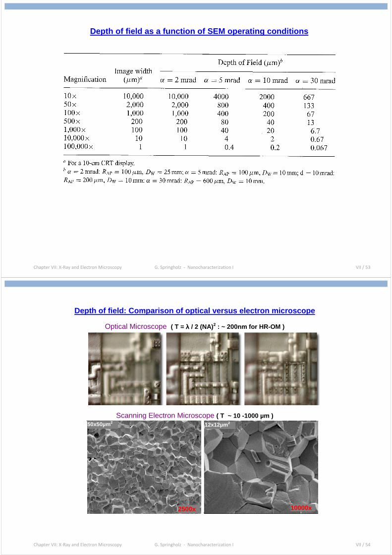
7.5.5 Depth of Field and Depth of Focus
= Depth T over which the image is sharp .
Criterion: Depth over which the broadening B introduced by being out of focus is comparable or less than the given lateral resolution R or spot size dprobe.
Broadening at an offset T: B = T. tan αp = R
Depth of field of SEM: T = R / tan αp
Due to the very small aperture angles, the depth of field of SEM is two orders of magnitude larger compared to optical microscopes:
Optical Microscope: T = λ / 2 (NA)2 = 1.3 . R2 / λ [δ = 0.61 λ / NA]
At low magnification and low resolution R:
αp can be chosen to be very small ~ 1 mrad.
Therefore, depth of focus T is as large as 1 mm !
At high resolution :
αp ~ 10 mrad but the depth of focus is still above 2 µm !
T
R
B
αp
focal plane
Depth of focus
~R2
~R
Chapter VII: X-Ray and Electron Microscopy G. Springholz - Nanocharacterization I VII / 53
Depth of field as a function of SEM operating conditions
Chapter VII: X-Ray and Electron Microscopy G. Springholz - Nanocharacterization I VII / 54
Depth of field: Comparison of optical versus electron microscope
Optical Microscope ( T = λλλλ / 2 (NA)2 : ~ 200nm for HR-OM )
Scanning Electron Microscope ( T ~ 10 -1000 µm )
2500x
50x50µm 2
10000x
12x12µm 2

Chapter VII: X-Ray and Electron Microscopy G. Springholz - Nanocharacterization I VII / 55
7.5.6 SEM Imaging using Backscattered and Secondary Electron Emission
In SEM/STEM, the imaging signal is essentially the intensity of electrons emitted from the sample due to the electron bombardment. The emitted electrons consist of two main contributions, namely,
(i) Backscattered Electrons (BSE):
= Primary electrons backscattered from the sample with BSEI and BSEII components.
(ii) Secondary Electrons (SE):
= Electrons excited and knocked out by the primary electrons entering the sample (SEI) or by electrons knocked out when BSE leave the sample (SEII) or by secondary processes such as x-ray photons. Practically, all emitted electrons emitted with energy less than 50 eV are considered as SE.
Escape depth Z
Due to the rather short mean free path λλλλ of electrons in solids, actually only a small fraction of the BSE and SE electrons that are generated within a certain escape depth Z underneath the surface can actually escape from the sample and can be collected by an electron detector.
Chapter VII: X-Ray and Electron Microscopy G. Springholz - Nanocharacterization I VII / 56
Escape Depth
The escape depth Z of electrons is about 5 times the mean free path λ λ λ λ, of electrons in solids. The mean free path is strongly dependent on the electron energy as shown on the right hand side.
⇒⇒⇒⇒ Essentially all emitted secondary electrons stem from a very thin layer of 5 to 50 nm
(=5 x λ) of the sample surface, with a minimum escape depth at electron energies of ~50eV.
Minimum

Chapter VII: X-Ray and Electron Microscopy G. Springholz - Nanocharacterization I VII / 57
7.5.7 Spatial Distribution of Emitted Electrons
Secondary electrons with low kinetic energy: λ ~10 Å for metals, 100 Å for insulators. Zescape ~10nm
Backscattered electrons with higher kinetic energies: λ ~100 Å, i.e., Zescape = 50 nm. Within each type of emitted electrons (SE or BSE), different contributions can be distinguished. Contributions acco rding to right figure: BSE I: Localized directly backscattered
electrons from single large-angle elastic scattering near the primary electron spot.
BES II: Delocalized backscattered electrons from multiple small angle scattering events leaving the sample from more remote areas.
SEI: Localized secondary electrons
produced when the primary electrons enter into the sample.
SEII: Delocalized secondary electrons produce when BSEII electrons leave the sample.
Chapter VII: X-Ray and Electron Microscopy G. Springholz - Nanocharacterization I VII / 58
SEIII: There is an additional third contribution SEIII of remotely generated secondary electrons produced by electrons scattered from the inner walls of the SEM around the sample.
This creates a nearly constant background of secondary electrons within the SEM chamber.
All high-energy electrons within the sample chamber can produce such remote secondary electrons.
Example for distribution of electrons:
SEI and BSE I electrons are particularly important for high resolution SEM imaging because they come from a highly localized spot on the sample surface.
Due to their low energy of SEI they can be efficiently collected and detected and their shallow escape depth yields high resolution and surface sensitivity.

Chapter VII: X-Ray and Electron Microscopy G. Springholz - Nanocharacterization I VII / 59
Lateral Distribution of Backscattered Electrons
The BSEs consists of:
(i) a strongly localized BSEI
peak at primary beam spot.
(ii) a broad outer range of BSEII electrons.
(see below)
Monte Carlo Simulations:
Chapter VII: X-Ray and Electron Microscopy G. Springholz - Nanocharacterization I VII / 60
Lateral range of backscattered electrons
Total emission area = RBS ~ RKO range.
But: Majority of the BSE electrons come from a much more localized spot (see prev. Fig).
If one considers the range where x% of the BSE come from, this can be described as:
RBS (x%) = k% . RKO
where k% is the cut-off proportionality factor:
Both the RKO range as well as proportionality factor k% decrease with increasing Z number:
For higher Z materials, the BSE signal comes from a much smaller spot of the sample !
d / RKO
current d / RKO
current d / RKO
current
k%
cuk%
cu

Chapter VII: X-Ray and Electron Microscopy G. Springholz - Nanocharacterization I VII / 61
Lateral Distribution of Secondary Electrons
The secondary electrons consist of two contributions :
SEI (SEBeam) and SEII (=SEBS), with and η = backscattering yield.
The area of SEI emission is ~ beam spot size: This yields high resolution SEM images.
The area of SEII emission is the same as that for BSEII electrons (~RKO).
Z-dependence:
The ratio of the generation efficiency between δBS and δB is about 3, but the contribution of the BS - SEII is proportional to the BS yield η , which increases with increasing Z.
Since for high Z materials RKO is smaller, in principle higher lateral resolution can is obtained for higher Z materials.
However, the total ratio of SEII / SEI is proportional to the BSE yield η, which increases with increasing Z number. Therefore, for high Z material less SE electrons come from the beam spot on the surface and the SE current is more dominated by the low resolution SEII contribution.
The increase in lateral resolution for high Z materials is less pronounced than for BSE electrons.
Chapter VII: X-Ray and Electron Microscopy G. Springholz - Nanocharacterization I VII / 62
7.5.8 Energy Distribution of Emitted Electrons and Energy Filtering
The different electron contributions can be actually distinguished due to their different emission energy:
Right hand figure:
Typical energy spectrum of emitted electrons
BSE I : Electrons with energy close to the primary electrons (low loss electrons).
BSE II: Electrons with intermediate energies.
SEI,II,III: Electrons with very low kinetic energies of up to about 20 eV.
By energy selective electron detection , the different contributions can be enhanced or suppressed.
This is achieved, e.g., by using an Evenhart-Thornley electron detector .
Chapter VII: X-Ray and Electron Microscopy G. Springholz - Nanocharacterization I VII / 63
Energy Filtering by Electron Detectors
Evenhart-Thornley detector: For high-sensitivity detection of the small electron currents (nA) emitted from the sample, a scintillator-photomultiplier detector is used, in which the emitted electrons are first converted to photons and subsequently amplified by a high gain photomultiplier. Energy filtering using a collector grid:
(a) Large positive bias (attraction of electrons): High collection efficiency for all types of electrons. Thus, the image intensity (current) is high but the spatial resolution low.
(b) Small negative bias (repulsion): Suppression of low-energy secondary electrons SE, detection only of BSE.
(c) Large negative bias (strong repulsion): Collection of only the directly backscattered BSEI electrons for high spatial resolution.
Semiconductor pn/Shottky junction detector: Impinging electrons create electron hole pairs, causing a current across the reversely biased pn junction.The average number of electron-hole pairs per incident electron is roughly equal to ~ E0/Egap, where Egap is the semiconductor band gap. Thus, high energy electrons give a higher signal, therefore, this dector is mainly used for backscattered electrons .
Chapter VII: X-Ray and Electron Microscopy G. Springholz - Nanocharacterization I VII / 64
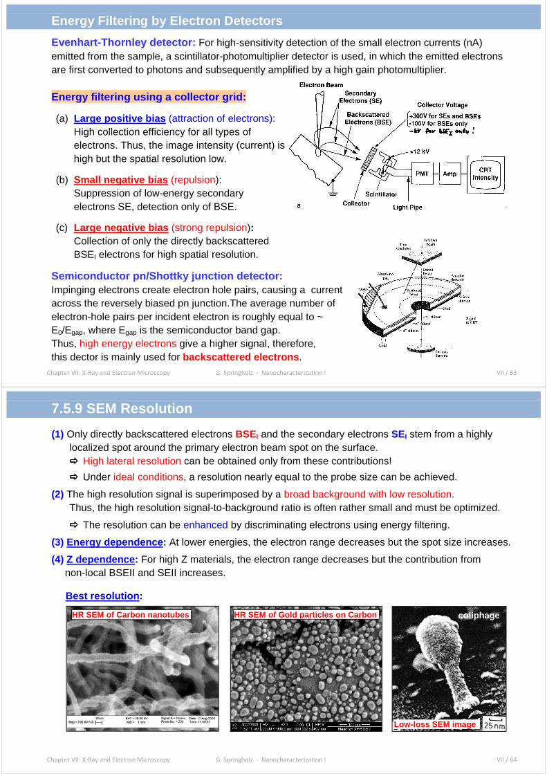
7.5.9 SEM Resolution
(1) Only directly backscattered electrons BSE I and the secondary electrons SEI stem from a highly localized spot around the primary electron beam spot on the surface. High lateral resolution can be obtained only from these contributions!
Under ideal conditions, a resolution nearly equal to the probe size can be achieved.
(2) The high resolution signal is superimposed by a broad background with low resolution. Thus, the high resolution signal-to-background ratio is often rather small and must be optimized.
The resolution can be enhanced by discriminating electrons using energy filtering.
(3) Energy dependence: At lower energies, the electron range decreases but the spot size increases.
(4) Z dependence: For high Z materials, the electron range decreases but the contribution from non-local BSEII and SEII increases.
Best resolution: In SE mode down to <3 nm, for low-loss BSE mode down to <5 nm achievable.
coliphage.
Low-loss SEM image
HR SEM of Gold particles on Carbon HR SEM of Carbon nanotubes

Chapter VII: X-Ray and Electron Microscopy G. Springholz - Nanocharacterization I VII / 65
Increased Resolution for Backscattered Electrons by E nergy Filtering Directly backscattered electrons BSEI with very small energy loss originate from the impingement area of highly focused electron beam: » High resolution imaging possible also with BS electrons. Backscattered electrons BSE II with larger energy loss stem from much larger area
with a size that increases with increasing Z and increasing E0.
Lateral resolution of BSE signal: deff = (d2probe + d2
BSE)1/2 where dBSE is the emission range for BSE.
» dBSE can be strongly reduced by energy filtering of the BSE signal by the detector.
» High-resolution low-loss BSE images using negatively biased ET or semiconductor detectors.
» But: dBSE is always proportional to RKO: Higher resolution achieved for larger Z and smaller Eprobe.
∆∆∆∆E < 1keV
Chapter VII: X-Ray and Electron Microscopy G. Springholz - Nanocharacterization I VII / 66
7.5.10 Contrast in SEM
A. Chemical Contrast - Backscattered Electrons (BS) The backscattering yield ηηηη is defined as n0 = number of primary electrons Empirical dependence of BS yield η as a function of atomic number Z (=Z-contrast):
General trends:
Increase of η as a function of atomic number Z because Rutherford backscattering is more efficient for heavy atoms.
The backscattering η yield does not show a significant beam energy dependence.
The contrast C in backscattered electron images is mainly due to differences in chemical compo-sition in the sample (but also contains some contributions of morphology) and is given by:
with
Ci is the concentration of the element i within the interaction volume of the sample.

Chapter VII: X-Ray and Electron Microscopy G. Springholz - Nanocharacterization I VII / 67
Examples for Z contrast in SEM:
.
Al-Ni alloy:
BSE electrons Specimen current
Ni-Cd battery element: SE: topo BSE: Z cotrast
ISC = Iprobe - IBS
Ni
Cd
Chapter VII: X-Ray and Electron Microscopy G. Springholz - Nanocharacterization I VII / 68
B. Topographic Contrast Topography contrast originates from: a) Surface tilt contrast due to
dependence
of SE and BSE yields on local surface
tilt relative to electron beam.
b) Shadowing contrast due to orientation
of electron collection detector relative
to the sample surface.
c) Diffusion contrast due to enhanced
SE escape probability at step
edges.
||
S ~ slope
+ shadowing
roundig of edges

Chapter VII: X-Ray and Electron Microscopy G. Springholz - Nanocharacterization I VII / 69
Topographic Contrast
Dependence of secondary electron yield as a function of the tilt angle θ between the primary beam and the surface normal is: Origin : For grazing incident primary electrons the trajectories are closer to the surface. Thus, more secondary electrons are generated within the escape depth of the surface. » Drastic increase of SE electron yield
with increasing surface tilt angle. » Very strong topographic contrast for
secondary electrons as compared to BS electrons.
SE mode BSE mode
BSE mode
SE mode
Chapter VII: X-Ray and Electron Microscopy G. Springholz - Nanocharacterization I VII / 70
Shadowing Contrast and its Control by the Detector Bi as High-energy BS electrons: Detected only when directly hit the detector » very strong shadowing effects
Secondary SE electrons: Due to positive detector bias, a large fraction of SE is collected by the detector.
SE:
BSE:

Chapter VII: X-Ray and Electron Microscopy G. Springholz - Nanocharacterization I VII / 71
Contrast tuning using different detectors as well as s pecimen current signal: Additional large area solid-state BSE detectors yield a high BSE collection efficiency and a BSE signal with reduced topographic contrast: This can be used to increase the chemical contrast and to suppress the topography contrast in the BSE images. A segmented BSE detector allows an additional contrast tuning. Z-contrast: (A+B) Topo = (A-B);
Specimen current: Is = Iprobe (1 – ηηηηBS – δδδδSE): same Z dependence as BSE electrons:
Chapter VII: X-Ray and Electron Microscopy G. Springholz - Nanocharacterization I VII / 72
7.6 Summary X-ray and electron microscopy can provide a much higher resolution due to the much
shorter wavelength of x-rays and electrons compared to visible light. However, both techniques represent cases where the actual achievable resolution is mostly limited by lens aberrations and not so much by the wavelength.
EUV and X-ray microscopy:
The realization of EUV and x-ray microscopes is difficult. The reasons is region: (i) the absorption of all materials becomes large, i.e., not transparent media are available and (ii) the refractive index of all materials is close to one.
Therefore, no simple optical systems can be made, but complicated reflective multilayer or diffractive optics (Fresnel zone plates) must be used. Also, no simple light sources are available.
Electron microscopy:
For electrons or charged particles, electro-magnetic lenses are used as optical elements, in which non-uniform electric or magnetic fields are used to obtain a focusing action.
The lens aberrations of electro-magnetic lenses are much larger than for optical lenses, and only limited aberration corrections are available.
Therefore, resolution of electron microscopy is mainly limited by the lens aberrations.
As a result an optimum aperture angle of the order α < 1° exists for which the resolution is maximized for a given lens system and electron energy.