Chapter 6 & 7: Field-Effect Transistors and...
69
Chapter 6 & 7: Field-Effect Transistors and Applications © Modified by Yuttapong Jiraraksopakun ENE, KMUTT 2009
Transcript of Chapter 6 & 7: Field-Effect Transistors and...

Chapter 6 & 7:
Field-Effect Transistors and Applications© Modified by Yuttapong Jiraraksopakun
ENE, KMUTT 2009

Copyright ©2009 by Pearson Education, Inc.
Upper Saddle River, New Jersey 07458 • All rights reserved.
Electronic Devices and Circuit Theory, 10/e
Robert L. Boylestad and Louis Nashelsky
Similarities: • Amplifiers
• Switching devices
• Impedance matching circuits
Differences:• FETs are voltage controlled devices. BJTs are current controlled
devices.
• FETs have a higher input impedance. BJTs have higher gains.
• FETs are less sensitive to temperature variations and are more easily
integrated on ICs.
• FETs are generally more static sensitive than BJTs.
FETs vs. BJTs
2

Copyright ©2009 by Pearson Education, Inc.
Upper Saddle River, New Jersey 07458 • All rights reserved.
Electronic Devices and Circuit Theory, 10/e
Robert L. Boylestad and Louis Nashelsky
•JFET: Junction FET
•MOSFET: Metal–Oxide–Semiconductor FET
�D-MOSFET: Depletion MOSFET
�E-MOSFET: Enhancement MOSFET
FET Types
3

Copyright ©2009 by Pearson Education, Inc.
Upper Saddle River, New Jersey 07458 • All rights reserved.
Electronic Devices and Circuit Theory, 10/e
Robert L. Boylestad and Louis Nashelsky
JFET Construction
There are two types of JFETs
•n-channel
•p-channel
The n-channel is more widely used.
There are three terminals:
•Drain (D) and Source (S) are connected to the n-channel
•Gate (G) is connected to the p-type material
4

Copyright ©2009 by Pearson Education, Inc.
Upper Saddle River, New Jersey 07458 • All rights reserved.
Electronic Devices and Circuit Theory, 10/e
Robert L. Boylestad and Louis Nashelsky
JFET Operation: The Basic Idea
JFET operation can be compared to a water spigot.
The source of water pressure is the
accumulation of electrons at the
negative pole of the drain-source
voltage.
The drain of water is the electron
deficiency (or holes) at the positive
pole of the applied voltage.
The control of flow of water is the
gate voltage that controls the width
of the n-channel and, therefore, the
flow of charges from source to
drain.
5

Copyright ©2009 by Pearson Education, Inc.
Upper Saddle River, New Jersey 07458 • All rights reserved.
Electronic Devices and Circuit Theory, 10/e
Robert L. Boylestad and Louis Nashelsky
JFET Operating Characteristics
There are three basic operating conditions for a JFET:
• VGS= 0, V
DSincreasing to some positive value
• VGS< 0, V
DSat some positive value
• Voltage-controlled resistor
6

Copyright ©2009 by Pearson Education, Inc.
Upper Saddle River, New Jersey 07458 • All rights reserved.
Electronic Devices and Circuit Theory, 10/e
Robert L. Boylestad and Louis Nashelsky
JFET Operating Characteristics: VGS
= 0 V
• The depletion region between p-gate
and n-channel increases as electrons
from n-channel combine with holes
from p-gate.
• Increasing the depletion region,
decreases the size of the n-channel
which increases the resistance of the
n-channel.
• Even though the n-channel resistance
is increasing, the current (ID) from
source to drain through the n-
channel is increasing. This is because
VDS is increasing.
Three things happen when VGS = 0 and VDS is increased from 0 to a more positive
voltage
7

Copyright ©2009 by Pearson Education, Inc.
Upper Saddle River, New Jersey 07458 • All rights reserved.
Electronic Devices and Circuit Theory, 10/e
Robert L. Boylestad and Louis Nashelsky
If VGS = 0 and VDS is further increased to
a more positive voltage, then the
depletion zone gets so large that it
pinches off the n-channel.
This suggests that the current in the n-
channel (ID) would drop to 0A, but it does
just the opposite–as VDS increases, so does
ID.
JFET Operating Characteristics: Pinch Off
8

Copyright ©2009 by Pearson Education, Inc.
Upper Saddle River, New Jersey 07458 • All rights reserved.
Electronic Devices and Circuit Theory, 10/e
Robert L. Boylestad and Louis Nashelsky
At the pinch-off point:
• Any further increase in VGS does not
produce any increase in ID. VGS at
pinch-off is denoted as Vp.
• ID is at saturation or maximum. It is
referred to as IDSS.
• The ohmic value of the channel is
maximum.
JFET Operating Characteristics: Saturation
9
Copyright ©2009 by Pearson Education, Inc.
Upper Saddle River, New Jersey 07458 • All rights reserved.
Electronic Devices and Circuit Theory, 10/e
Robert L. Boylestad and Louis Nashelsky
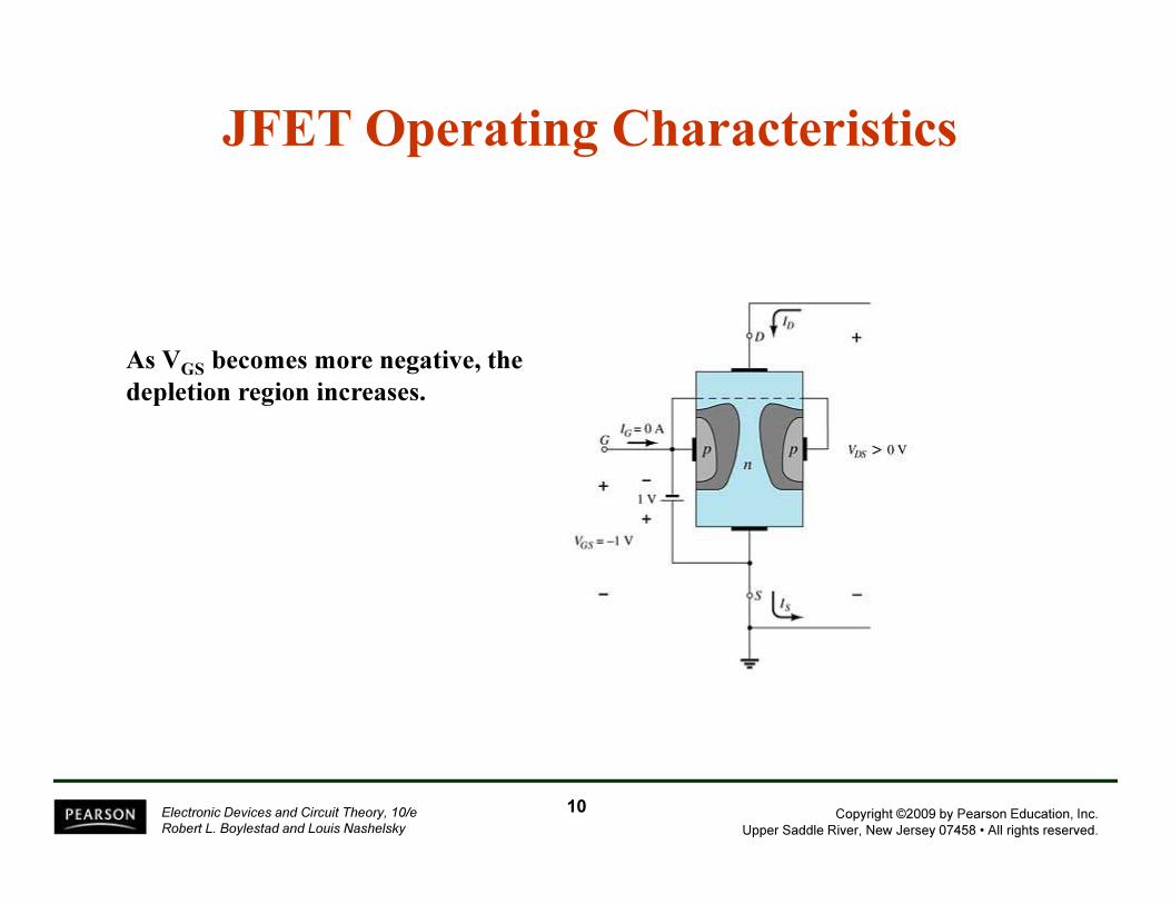
JFET Operating Characteristics
As VGS becomes more negative, the
depletion region increases.
10

Copyright ©2009 by Pearson Education, Inc.
Upper Saddle River, New Jersey 07458 • All rights reserved.
Electronic Devices and Circuit Theory, 10/e
Robert L. Boylestad and Louis Nashelsky
As VGS becomes more negative:
• The JFET experiences
pinch-off at a lower voltage
(VP).
• ID decreases (ID < IDSS) even
though VDS is increased.
• Eventually ID reaches 0 A.
VGS at this point is called Vp
or VGS(off)..
JFET Operating Characteristics
Also note that at high levels of VDS the JFET reaches a breakdown situation. ID
increases uncontrollably if VDS > VDSmax.
11

Copyright ©2009 by Pearson Education, Inc.
Upper Saddle River, New Jersey 07458 • All rights reserved.
Electronic Devices and Circuit Theory, 10/e
Robert L. Boylestad and Louis Nashelsky
2
P
GS
od
V
V1
rr
−
=
The region to the left of the
pinch-off point is called the
ohmic region.
The JFET can be used as a
variable resistor, where VGS
controls the drain-source
resistance (rd). As VGS becomes
more negative, the resistance
(rd) increases.
JFET Operating Characteristics:
Voltage-Controlled Resistor
12

Copyright ©2009 by Pearson Education, Inc.
Upper Saddle River, New Jersey 07458 • All rights reserved.
Electronic Devices and Circuit Theory, 10/e
Robert L. Boylestad and Louis Nashelsky
p-Channel JFETS
The p-channel JFET behaves the
same as the n-channel JFET,
except the voltage polarities and
current directions are reversed.
13

Copyright ©2009 by Pearson Education, Inc.
Upper Saddle River, New Jersey 07458 • All rights reserved.
Electronic Devices and Circuit Theory, 10/e
Robert L. Boylestad and Louis Nashelsky
p-Channel JFET Characteristics
Also note that at high levels of VDS the JFET reaches a breakdown situation: ID
increases uncontrollably if VDS > VDSmax.
As VGS increases more positively
• The depletion zone
increases
• ID decreases (ID < IDSS)
• Eventually ID = 0 A
14

Copyright ©2009 by Pearson Education, Inc.
Upper Saddle River, New Jersey 07458 • All rights reserved.
Electronic Devices and Circuit Theory, 10/e
Robert L. Boylestad and Louis Nashelsky
N-Channel JFET Symbol
15

Copyright ©2009 by Pearson Education, Inc.
Upper Saddle River, New Jersey 07458 • All rights reserved.
Electronic Devices and Circuit Theory, 10/e
Robert L. Boylestad and Louis Nashelsky
2
V
V1DSSD
P
GSII
−=
The transfer characteristic of input-to-output is not as straightforward in
a JFET as it is in a BJT.
In a BJT, β indicates the relationship between IB (input) and IC (output).
In a JFET, the relationship of VGS (input) and ID (output) is a little more
complicated:
JFET Transfer Characteristics
16
Copyright ©2009 by Pearson Education, Inc.
Upper Saddle River, New Jersey 07458 • All rights reserved.
Electronic Devices and Circuit Theory, 10/e
Robert L. Boylestad and Louis Nashelsky
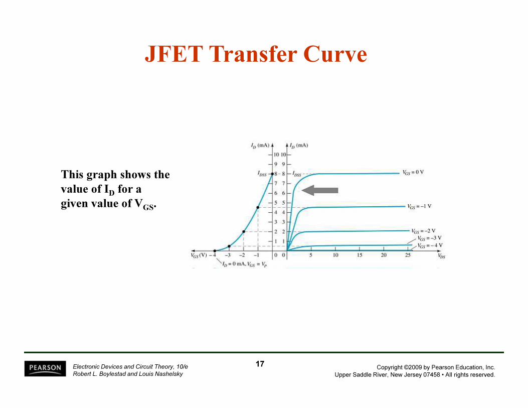
JFET Transfer Curve
This graph shows the
value of ID for a
given value of VGS.
17

Copyright ©2009 by Pearson Education, Inc.
Upper Saddle River, New Jersey 07458 • All rights reserved.
Electronic Devices and Circuit Theory, 10/e
Robert L. Boylestad and Louis Nashelsky
Using IDSS and Vp (VGS(off)) values found in a specification sheet, the transfer
curve can be plotted according to these three steps:
Solving for VGS = 0V ID = IDSS
2
P
GSDSSD
V
V1II
−=
Step 1
Solving for VGS = Vp (VGS(off)) ID = 0A
2
P
GSDSSD
V
V1II
−=
Step 2
Solving for VGS = 0V to Vp
2
P
GSDSSD
V
V1II
−=
Step 3
Plotting the JFET Transfer Curve
18

Copyright ©2009 by Pearson Education, Inc.
Upper Saddle River, New Jersey 07458 • All rights reserved.
Electronic Devices and Circuit Theory, 10/e
Robert L. Boylestad and Louis Nashelsky
JFET Specifications Sheet
Electrical Characteristics
19

Copyright ©2009 by Pearson Education, Inc.
Upper Saddle River, New Jersey 07458 • All rights reserved.
Electronic Devices and Circuit Theory, 10/e
Robert L. Boylestad and Louis Nashelsky
JFET Specifications Sheet
Maximum Ratings
more…
20

Copyright ©2009 by Pearson Education, Inc.
Upper Saddle River, New Jersey 07458 • All rights reserved.
Electronic Devices and Circuit Theory, 10/e
Robert L. Boylestad and Louis Nashelsky
Case and Terminal Identification
21

Copyright ©2009 by Pearson Education, Inc.
Upper Saddle River, New Jersey 07458 • All rights reserved.
Electronic Devices and Circuit Theory, 10/e
Robert L. Boylestad and Louis Nashelsky
MOSFETs
There are two types of MOSFETs:
• Depletion-Type
• Enhancement-Type
MOSFETs have characteristics similar to JFETs and additional
characteristics that make then very useful.
22

Copyright ©2009 by Pearson Education, Inc.
Upper Saddle River, New Jersey 07458 • All rights reserved.
Electronic Devices and Circuit Theory, 10/e
Robert L. Boylestad and Louis Nashelsky
Depletion-Type MOSFET Construction
The Drain (D) and Source (S) connect
to the to n-doped regions. These n-
doped regions are connected via an n-
channel. This n-channel is connected to
the Gate (G) via a thin insulating layer
of SiO2.
The n-doped material lies on a p-doped
substrate that may have an additional
terminal connection called Substrate
(SS).
23

Copyright ©2009 by Pearson Education, Inc.
Upper Saddle River, New Jersey 07458 • All rights reserved.
Electronic Devices and Circuit Theory, 10/e
Robert L. Boylestad and Louis Nashelsky
Basic MOSFET Operation
A depletion-type MOSFET can operate in two modes:
• Depletion mode
• Enhancement mode
24

Copyright ©2009 by Pearson Education, Inc.
Upper Saddle River, New Jersey 07458 • All rights reserved.
Electronic Devices and Circuit Theory, 10/e
Robert L. Boylestad and Louis Nashelsky
D-Type MOSFET in Depletion Mode
• When VGS = 0 V, ID = IDSS
• When VGS < 0 V, ID < IDSS
• The formula used to plot the transfer
curve still applies:
Depletion Mode
The characteristics are similar
to a JFET.
2
P
GSDSSD
V
V1II
−=
25

Copyright ©2009 by Pearson Education, Inc.
Upper Saddle River, New Jersey 07458 • All rights reserved.
Electronic Devices and Circuit Theory, 10/e
Robert L. Boylestad and Louis Nashelsky
D-Type MOSFET in Enhancement Mode
• VGS > 0 V
• ID increases above IDSS
• The formula used to plot
the transfer curve still
applies:2
P
GSDSSD
V
V1II
−=
Enhancement Mode
Note that VGS is now a positive polarity
26

Copyright ©2009 by Pearson Education, Inc.
Upper Saddle River, New Jersey 07458 • All rights reserved.
Electronic Devices and Circuit Theory, 10/e
Robert L. Boylestad and Louis Nashelsky
p-Channel D-Type MOSFET
27

Copyright ©2009 by Pearson Education, Inc.
Upper Saddle River, New Jersey 07458 • All rights reserved.
Electronic Devices and Circuit Theory, 10/e
Robert L. Boylestad and Louis Nashelsky
D-Type MOSFET Symbols
28

Copyright ©2009 by Pearson Education, Inc.
Upper Saddle River, New Jersey 07458 • All rights reserved.
Electronic Devices and Circuit Theory, 10/e
Robert L. Boylestad and Louis Nashelsky
Maximum Ratings
more…
Specification Sheet
29

Copyright ©2009 by Pearson Education, Inc.
Upper Saddle River, New Jersey 07458 • All rights reserved.
Electronic Devices and Circuit Theory, 10/e
Robert L. Boylestad and Louis Nashelsky
Electrical Characteristics
Specification Sheet
30

Copyright ©2009 by Pearson Education, Inc.
Upper Saddle River, New Jersey 07458 • All rights reserved.
Electronic Devices and Circuit Theory, 10/e
Robert L. Boylestad and Louis Nashelsky
E-Type MOSFET Construction
• The Drain (D) and Source (S) connect
to the to n-doped regions. These n-
doped regions are connected via an n-
channel
• The Gate (G) connects to the p-doped
substrate via a thin insulating layer of
SiO2
• There is no channel
• The n-doped material lies on a p-doped
substrate that may have an additional
terminal connection called the
Substrate (SS)
31

Copyright ©2009 by Pearson Education, Inc.
Upper Saddle River, New Jersey 07458 • All rights reserved.
Electronic Devices and Circuit Theory, 10/e
Robert L. Boylestad and Louis Nashelsky
Basic Operation of the E-Type MOSFET
• VGS is always positive
• As VGS increases, IDincreases
• As VGS is kept constant
and VDS is increased,
then ID saturates (IDSS)
and the saturation level,
VDSsat is reached
The enhancement-type MOSFET operates only in the enhancement mode.
32
Copyright ©2009 by Pearson Education, Inc.
Upper Saddle River, New Jersey 07458 • All rights reserved.
Electronic Devices and Circuit Theory, 10/e
Robert L. Boylestad and Louis Nashelsky
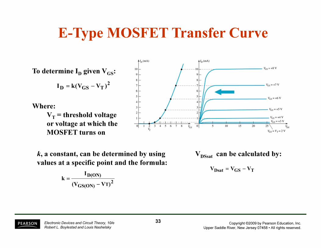
E-Type MOSFET Transfer Curve
To determine ID given VGS:
Where:
VT = threshold voltage
or voltage at which the
MOSFET turns on
2TGSD )VV(kI −=
k, a constant, can be determined by using
values at a specific point and the formula:
2TGS(ON)
D(ON)
)V(V
Ik
−
=
VDSsat can be calculated by:
TGSDsat VVV −=
33

Copyright ©2009 by Pearson Education, Inc.
Upper Saddle River, New Jersey 07458 • All rights reserved.
Electronic Devices and Circuit Theory, 10/e
Robert L. Boylestad and Louis Nashelsky
p-Channel E-Type MOSFETs
The p-channel enhancement-type MOSFET is similar to the n-
channel, except that the voltage polarities and current directions
are reversed.
34

Copyright ©2009 by Pearson Education, Inc.
Upper Saddle River, New Jersey 07458 • All rights reserved.
Electronic Devices and Circuit Theory, 10/e
Robert L. Boylestad and Louis Nashelsky
MOSFET Symbols
35

Copyright ©2009 by Pearson Education, Inc.
Upper Saddle River, New Jersey 07458 • All rights reserved.
Electronic Devices and Circuit Theory, 10/e
Robert L. Boylestad and Louis Nashelsky
Maximum Ratings
more…
Specification Sheet
36

Copyright ©2009 by Pearson Education, Inc.
Upper Saddle River, New Jersey 07458 • All rights reserved.
Electronic Devices and Circuit Theory, 10/e
Robert L. Boylestad and Louis Nashelsky
Electrical Characteristics
Specification Sheet
37

Copyright ©2009 by Pearson Education, Inc.
Upper Saddle River, New Jersey 07458 • All rights reserved.
Electronic Devices and Circuit Theory, 10/e
Robert L. Boylestad and Louis Nashelsky
Handling MOSFETs
MOSFETs are very sensitive to static electricity. Because of the very thin
SiO2 layer between the external terminals and the layers of the device,
any small electrical discharge can create an unwanted conduction.
Protection
• Always transport in a static sensitive bag
• Always wear a static strap when handling MOSFETS
•
• Apply voltage limiting devices between the gate and source, such as
back-to-back Zeners to limit any transient voltage.
38

Copyright ©2009 by Pearson Education, Inc.
Upper Saddle River, New Jersey 07458 • All rights reserved.
Electronic Devices and Circuit Theory, 10/e
Robert L. Boylestad and Louis Nashelsky
VMOS Devices
VMOS (vertical MOSFET)
increases the surface area of
the device.
Advantages
• VMOS devices handle
higher currents by
providing more surface
area to dissipate the heat.
• VMOS devices also have
faster switching times.
39

Copyright ©2009 by Pearson Education, Inc.
Upper Saddle River, New Jersey 07458 • All rights reserved.
Electronic Devices and Circuit Theory, 10/e
Robert L. Boylestad and Louis Nashelsky
Advantages
• Useful in logic circuit designs
• Higher input impedance
• Faster switching speeds
• Lower operating power levels
CMOS Devices
CMOS (complementary
MOSFET) uses a p-channel
and n-channel MOSFET;
often on the same substrate as
shown here.
40

Copyright ©2009 by Pearson Education, Inc.
Upper Saddle River, New Jersey 07458 • All rights reserved.
Electronic Devices and Circuit Theory, 10/e
Robert L. Boylestad and Louis Nashelsky
Summary Table
41

Copyright ©2009 by Pearson Education, Inc.
Upper Saddle River, New Jersey 07458 • All rights reserved.
Electronic Devices and Circuit Theory, 10/e
Robert L. Boylestad and Louis Nashelsky
Common FET Biasing Circuits
JFET Biasing Circuits
• Fixed – Bias
• Self-Bias
• Voltage-Divider Bias
D-Type MOSFET Biasing Circuits
•Self-Bias
•Voltage-Divider Bias
E-Type MOSFET Biasing Circuits
•Feedback Configuration
•Voltage-Divider Bias
42

Copyright ©2009 by Pearson Education, Inc.
Upper Saddle River, New Jersey 07458 • All rights reserved.
Electronic Devices and Circuit Theory, 10/e
Robert L. Boylestad and Louis Nashelsky
Basic Current Relationships
For all FETs:
A0IG ≅
SD II =
For JFETS and D-Type MOSFETs:
2
P
GSDSSD
V
V1II
−=
For E-Type MOSFETs:
2TGSD )VV(kI −=
43

Copyright ©2009 by Pearson Education, Inc.
Upper Saddle River, New Jersey 07458 • All rights reserved.
Electronic Devices and Circuit Theory, 10/e
Robert L. Boylestad and Louis Nashelsky
GGGS
GS
DSC
S
DDDDDS
VV
VV
VV
V0V
RIVV
−=
=
=
=
−=
Fixed-Bias Configuration
44

Copyright ©2009 by Pearson Education, Inc.
Upper Saddle River, New Jersey 07458 • All rights reserved.
Electronic Devices and Circuit Theory, 10/e
Robert L. Boylestad and Louis Nashelsky
Fixed-Bias Configuration
45

Copyright ©2009 by Pearson Education, Inc.
Upper Saddle River, New Jersey 07458 • All rights reserved.
Electronic Devices and Circuit Theory, 10/e
Robert L. Boylestad and Louis Nashelsky
Self-Bias Configuration
46

Copyright ©2009 by Pearson Education, Inc.
Upper Saddle River, New Jersey 07458 • All rights reserved.
Electronic Devices and Circuit Theory, 10/e
Robert L. Boylestad and Louis Nashelsky
RDDDSDSD
SDS
DSDDDDS
VVVVV
RIV
)RR(IVV
−=+=
=
+−=
SDGS RIV −=
To solve this equation:
• Select an ID < IDSS and use the component value of
RS to calculate VGS
• Plot the point identified by ID and VGS. Draw a
line from the origin of the axis to this point.
• Plot the transfer curve using IDSS and
VP (VP = VGSoff in specification sheets) and a few
points such as ID = IDSS / 4 and ID = IDSS / 2 etc.
Self-Bias CalculationsFor the indicated loop,
47
The Q-point is located where the first line
intersects the transfer curve. Use the value
of ID at the Q-point (IDQ) to solve for the
other voltages:

Copyright ©2009 by Pearson Education, Inc.
Upper Saddle River, New Jersey 07458 • All rights reserved.
Electronic Devices and Circuit Theory, 10/e
Robert L. Boylestad and Louis Nashelsky
Self-Bias Configuration
48

Copyright ©2009 by Pearson Education, Inc.
Upper Saddle River, New Jersey 07458 • All rights reserved.
Electronic Devices and Circuit Theory, 10/e
Robert L. Boylestad and Louis Nashelsky
Voltage-Divider Bias
IG = 0 A
ID responds to changes in
VGS.
49

Copyright ©2009 by Pearson Education, Inc.
Upper Saddle River, New Jersey 07458 • All rights reserved.
Electronic Devices and Circuit Theory, 10/e
Robert L. Boylestad and Louis Nashelsky
Voltage-Divider Bias Calculations
The Q point is established by plotting
a line that intersects the transfer
curve.
21
DD2G
RR
VRV
+
=
VG is equal to the voltage across
divider resistor R2:
Using Kirchhoff’s Law:
SDGGS RIVV −=
50

Copyright ©2009 by Pearson Education, Inc.
Upper Saddle River, New Jersey 07458 • All rights reserved.
Electronic Devices and Circuit Theory, 10/e
Robert L. Boylestad and Louis Nashelsky
Voltage-Divider Q-point
Step 1
Plot the line by plotting two points:
•VGS = VG, ID = 0 A
•VGS = 0 V, ID = VG / RS
Step 2
Plot the transfer curve by plotting
IDSS, VP and the calculated values
of ID
Step 3
The Q-point is located where the
line intersects the transfer curve
51

Copyright ©2009 by Pearson Education, Inc.
Upper Saddle River, New Jersey 07458 • All rights reserved.
Electronic Devices and Circuit Theory, 10/e
Robert L. Boylestad and Louis Nashelsky
Voltage-Divider Bias Calculations
Using the value of ID at the Q-point, solve for the other variables in the voltage-
divider bias circuit:
SDS
DDDDD
SDDDDDS
RIV
RIVV
)R(RIVV
=
−=
+−=
21
DDR2R1
RR
VII
+
==
52

Copyright ©2009 by Pearson Education, Inc.
Upper Saddle River, New Jersey 07458 • All rights reserved.
Electronic Devices and Circuit Theory, 10/e
Robert L. Boylestad and Louis Nashelsky
Voltage-Divider Bias Calculations
53

Copyright ©2009 by Pearson Education, Inc.
Upper Saddle River, New Jersey 07458 • All rights reserved.
Electronic Devices and Circuit Theory, 10/e
Robert L. Boylestad and Louis Nashelsky
D-Type MOSFET Bias Circuits
Depletion-type MOSFET bias
circuits are similar to those
used to bias JFETs. The only
difference is that depletion-type
MOSFETs can operate with
positive values of VGS and with
ID values that exceed IDSS.
54
Copyright ©2009 by Pearson Education, Inc.
Upper Saddle River, New Jersey 07458 • All rights reserved.
Electronic Devices and Circuit Theory, 10/e
Robert L. Boylestad and Louis Nashelsky
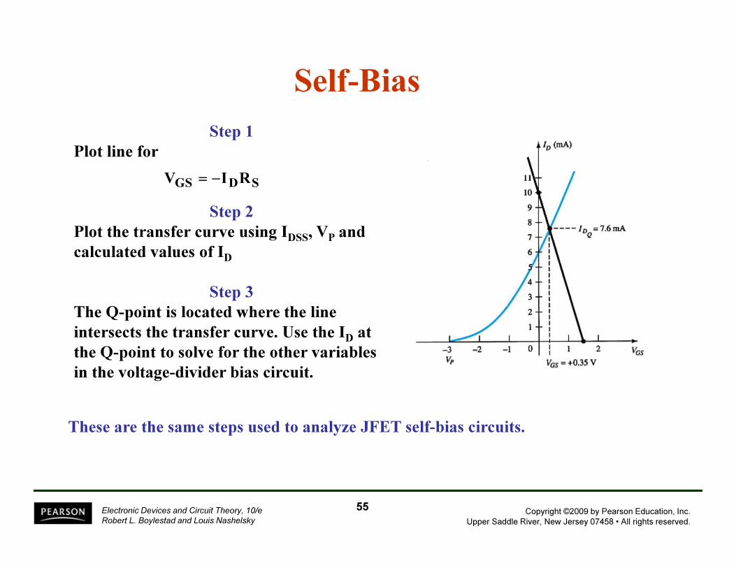
Self-Bias
Step 1
Plot line for
Step 2
Plot the transfer curve using IDSS, VP and
calculated values of ID
Step 3
The Q-point is located where the line
intersects the transfer curve. Use the ID at
the Q-point to solve for the other variables
in the voltage-divider bias circuit.
These are the same steps used to analyze JFET self-bias circuits.
55
SDGS RIV −=

Copyright ©2009 by Pearson Education, Inc.
Upper Saddle River, New Jersey 07458 • All rights reserved.
Electronic Devices and Circuit Theory, 10/e
Robert L. Boylestad and Louis Nashelsky
Self-Bias
56

Copyright ©2009 by Pearson Education, Inc.
Upper Saddle River, New Jersey 07458 • All rights reserved.
Electronic Devices and Circuit Theory, 10/e
Robert L. Boylestad and Louis Nashelsky
Voltage-Divider BiasStep 1
Plot the line for
•VGS = VG, ID = 0 A
•ID = VG/RS, VGS = 0 V
Step 2
Plot the transfer curve using IDSS, VP and
calculated values of ID.
Step 3
The Q-point is located where the line intersects
the transfer curve is. Use the ID at the Q-point
to solve for the other variables
in the voltage-divider bias circuit.
These are the same steps used to analyze
JFET voltage-divider bias circuits.
57

Copyright ©2009 by Pearson Education, Inc.
Upper Saddle River, New Jersey 07458 • All rights reserved.
Electronic Devices and Circuit Theory, 10/e
Robert L. Boylestad and Louis Nashelsky
Voltage-Divider Bias
58

Copyright ©2009 by Pearson Education, Inc.
Upper Saddle River, New Jersey 07458 • All rights reserved.
Electronic Devices and Circuit Theory, 10/e
Robert L. Boylestad and Louis Nashelsky
E-Type MOSFET Bias Circuits
The transfer characteristic for
the e-type MOSFET is very
different from that of a simple
JFET or the d-type MOSFET.
59

Copyright ©2009 by Pearson Education, Inc.
Upper Saddle River, New Jersey 07458 • All rights reserved.
Electronic Devices and Circuit Theory, 10/e
Robert L. Boylestad and Louis Nashelsky
Feedback Bias Circuit
IG = 0 A
VRG = 0 V
VDS = VGS
VGS = VDD – IDRD
60

Copyright ©2009 by Pearson Education, Inc.
Upper Saddle River, New Jersey 07458 • All rights reserved.
Electronic Devices and Circuit Theory, 10/e
Robert L. Boylestad and Louis Nashelsky
Feedback Bias Q-PointStep 1
Plot the line using
•VGS = VDD, ID = 0 A
•ID = VDD / RD , VGS = 0 V
Step 2
Using values from the specification
sheet, plot the transfer curve with
•VGSTh , ID = 0 A
•VGS(on), ID(on)
Step 3
The Q-point is located where the line
and the transfer curve intersect
Step 4
Using the value of ID at the Q-point,
solve for the other variables in the
bias circuit
61

Copyright ©2009 by Pearson Education, Inc.
Upper Saddle River, New Jersey 07458 • All rights reserved.
Electronic Devices and Circuit Theory, 10/e
Robert L. Boylestad and Louis Nashelsky
Feedback Bias Circuit
62

Copyright ©2009 by Pearson Education, Inc.
Upper Saddle River, New Jersey 07458 • All rights reserved.
Electronic Devices and Circuit Theory, 10/e
Robert L. Boylestad and Louis Nashelsky
Voltage-Divider Biasing
Plot the line and the transfer curve to find the
Q-point. Use these equations:
21
DD2G
RR
VRV
+
=
)RR(IVV
RIVV
DSDDDDS
SDGGS
+−=
−=
63
Copyright ©2009 by Pearson Education, Inc.
Upper Saddle River, New Jersey 07458 • All rights reserved.
Electronic Devices and Circuit Theory, 10/e
Robert L. Boylestad and Louis Nashelsky
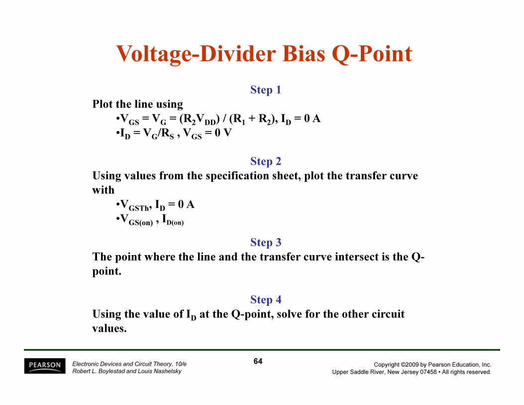
Voltage-Divider Bias Q-Point
Step 1
Plot the line using
•VGS = VG = (R2VDD) / (R1 + R2), ID = 0 A
•ID = VG/RS , VGS = 0 V
Step 2
Using values from the specification sheet, plot the transfer curve
with
•VGSTh, ID = 0 A
•VGS(on) , ID(on)
Step 3
The point where the line and the transfer curve intersect is the Q-
point.
Step 4
Using the value of ID at the Q-point, solve for the other circuit
values.
64

Copyright ©2009 by Pearson Education, Inc.
Upper Saddle River, New Jersey 07458 • All rights reserved.
Electronic Devices and Circuit Theory, 10/e
Robert L. Boylestad and Louis Nashelsky
Voltage-Divider Biasing
65

Copyright ©2009 by Pearson Education, Inc.
Upper Saddle River, New Jersey 07458 • All rights reserved.
Electronic Devices and Circuit Theory, 10/e
Robert L. Boylestad and Louis Nashelsky
p-Channel FETs
For p-channel FETs the same calculations and graphs are used,
except that the voltage polarities and current directions are reversed.
The graphs are mirror images of the n-channel graphs.
66

Copyright ©2009 by Pearson Education, Inc.
Upper Saddle River, New Jersey 07458 • All rights reserved.
Electronic Devices and Circuit Theory, 10/e
Robert L. Boylestad and Louis Nashelsky
Applications
Voltage-controlled resistor
JFET voltmeter
Timer network
Fiber optic circuitry
MOSFET relay driver
67
Copyright ©2009 by Pearson Education, Inc.
Upper Saddle River, New Jersey 07458 • All rights reserved.
Electronic Devices and Circuit Theory, 10/e
Robert L. Boylestad and Louis Nashelsky
Homework 4 (Chapter 6)
• Transfer Characteristics
– 6.3 (11, 12)
• Depletion-Type MOSFET
– 6.7 (28)
• Enhancement-Type MOSFET
– 6.8 (33, 36)
68

Copyright ©2009 by Pearson Education, Inc.
Upper Saddle River, New Jersey 07458 • All rights reserved.
Electronic Devices and Circuit Theory, 10/e
Robert L. Boylestad and Louis Nashelsky
Homework 4 (Chapter 7)
• Fixed-biased
– 7.2 (1)
• Self-biased
– 7.3 (6)
• Voltage-Divider
– 7.4 (12)
• Depletion-Type
– 7.5 (18)
• Enhancement-Type
– 7.6 (20)
69