Chapter - 5 Analysis and Modeling of Coplanar...
58
111 Chapter - 5 Analysis and Modeling of Coplanar Waveguide 5.1 Introduction Coplanar waveguides (CPW) are a type of planar transmission line used in MICs as well as in MMICs. The CPW is uniplanar in construction and it facilitates easy shunt, as well as series, surface mounting of active and passive devices. It also eliminates the need for wraparound and via holes, and further, it reduces radiation loss. Its characteristic impedance is determined by the ratio of central conductor width and gap between central conductor and ground. Its structure has influence on losses. The CPW is a low dispersion line, so it is suitable for development of wide-band circuits and components [60, 73, 105, 123, 134]. The CPW structure has several variations, like asymmetrical CPW (ACPW), the CPW with finite ground planes, conductor-backed CPW, CPW with top shield etc. These structures are also used with multilayer substrates [43,64,105]. Furthermore, the CPW structures have also been constructed on non-planar substrates like circular cylindrical and elliptical cylindrical structures [19, 52, 55, 84, 90, 105, 130]. Several rigorous methods, including the spectral domain analysis (SDA), and experimental investigations have been used to determine the line parameters of the standard CPW line [73,105]. The commercial EM-simulators, such as Ansoft HFSS, Sonnet, CST Microwave Studio etc., are in use to analyze the CPW based circuits. However, these are not convenient for interactive design CAD tool of the CPW structures. The conformal mapping method, discussed in Chapter-3, is used to get design oriented expressions to compute the static characteristic impedance and static effective relative permittivity of varieties of CPW structures, both planar and non-planar, single- layer substrate and multilayer substrate. However, for most of the CPW structures
Transcript of Chapter - 5 Analysis and Modeling of Coplanar...

111
Chapter - 5
Analysis and Modeling of Coplanar Waveguide
5.1 Introduction
Coplanar waveguides (CPW) are a type of planar transmission line used in MICs as well
as in MMICs. The CPW is uniplanar in construction and it facilitates easy shunt, as well
as series, surface mounting of active and passive devices. It also eliminates the need for
wraparound and via holes, and further, it reduces radiation loss. Its characteristic
impedance is determined by the ratio of central conductor width and gap between central
conductor and ground. Its structure has influence on losses. The CPW is a low dispersion
line, so it is suitable for development of wide-band circuits and components [60, 73, 105,
123, 134]. The CPW structure has several variations, like asymmetrical CPW (ACPW),
the CPW with finite ground planes, conductor-backed CPW, CPW with top shield etc.
These structures are also used with multilayer substrates [43,64,105]. Furthermore, the
CPW structures have also been constructed on non-planar substrates like circular
cylindrical and elliptical cylindrical structures [19, 52, 55, 84, 90, 105, 130].
Several rigorous methods, including the spectral domain analysis (SDA), and
experimental investigations have been used to determine the line parameters of the
standard CPW line [73,105]. The commercial EM-simulators, such as Ansoft HFSS,
Sonnet, CST Microwave Studio etc., are in use to analyze the CPW based circuits.
However, these are not convenient for interactive design CAD tool of the CPW
structures. The conformal mapping method, discussed in Chapter-3, is used to get design
oriented expressions to compute the static characteristic impedance and static effective
relative permittivity of varieties of CPW structures, both planar and non-planar, single-
layer substrate and multilayer substrate. However, for most of the CPW structures

Analysis and Modeling of CPW
112
dispersion is not considered through closed-form expressions, except in the case of
standard planar CPW on finite thickness single-layer substrate with infinite extent ground
planes [18,73,105]. Likewise, losses have been computed only for this standard planar
CPW [21,48,96]. Even the dispersion expression of the standard planar CPW does not
account for finite thickness of the strip conductors. Thus there is need to extend the
dispersion expression with finite strip conductor thickness to the planar and non-planar
CPW under multilayer environment. The methods to compute dielectric loss and
conductor loss are also to be extended for these more general CPW structures.
In this chapter, we present the analysis and modeling of conductor thickness and
frequency dependent line parameters of different configurations of CPW. Their design
and analysis are discussed in detail. Two different methods for conductor loss
computation i.e. Wheeler’s incremental inductance formulation and perturbation method
with the concept of stopping distance have been used. The effects of strip asymmetry, top
shield and conductor backing on the characteristics of CPW are also analyzed. All the
developed models are further extended to the non-planar (elliptical and circular
cylindrical) CPW. The models are used with the multilayered substrates, both planar and
non-planar, with the help of single layer formulation (SLR), summarized in Chapter-4.
Lastly, the circuit models are developed to account for low frequency features. All
developed models are verified against available experimental results and the results
obtained using the EM- simulators over wide range of parameters.
Fig.(5.1): Cross section of coplanar transmission line.

Analysis and Modeling of CPW
113
5.2 Effect of Conductor Thickness on Characteristics of CPW
Fig. (5.1) shows the CPW with central strip width 2a = s, ground-to-ground inner spacing
2b = (s + 2w), ground-to-ground outer spacing 2c, substrate thickness h and conductor
thickness t with relative permittivity rε . The conductor thickness independent expressions
for the effective relative permittivity effε and the characteristic impedance Z0 of the CPW
with ∞→c , using the conformal mapping method are obtained from equations-(3.15)
and (3.16) respectively.
)'k(K
)k(K
)k(K
)'k(Kreff
1
1
0
0
2
11
−+=
εε (5.1)
)k(K
)'k(KZ
eff 0
00
30
επ= (5.2)
where modulus 0k and 1k , along with their complementary modulus '0k and '
1k , are
defined in equations-(3.10) -(3.12). However, we modify these expressions empirically to
take into account the finite strip conductor thickness t [73]. The equivalent slot-width weq
is reduced slot-width with zero conductor thickness; whereas the equivalent strip-width
seq is enlarged one.
)iv(t
w
s
t
h
tln.)ln(
ts
elyAlternativ)iii(t
wln
ts
)ii(sww)i(sss
r
eqeq
+
−+=
+=
−=+=
πππ
∆
ππε
∆
∆∆
85041
81
2
22
(5.3)
The aspect-ratio 0k and 1k are replaced by the modified aspect ratio t,0k and
t,1k
respectively, that takes care of the strip conductor thickness.

Analysis and Modeling of CPW
114
)ii(k1k)i(w2s
sk 2
t,0'
t,0eqeq
eqt,0 −=
+= (5.4)
)ii(k1'k)i(
)w2s(h4
sinh
h4
ssinh
k 2t,1t,1
eqeq
eq
t,1 −=
+
=π
π
(5.5)
The effective relative permittivity of the CPW with conductor thickness is computed
from the following empirical relation [73]
)/(.)](/)([
/])([.)()(
' wt70kKkK
wt10t700tt
00
effeffeff
+
−=−==
εεε (5.6)
The characteristic impedance of the CPW with conductor thickness t is computed from
the equation-(5.2) after using conductor thickness dependent effective relative
permittivity and modified aspect-ratio [18]:
( ))k(K
)k(K
)t(tZ
t,
't,
eff 0
00
30
επ=
(5.7)
The conductor thickness has more effect on 0Z as compared to its effect on effε [22].
5.3 Dispersion in CPW
Frankel et. al. [91] verified the analytic dispersion expressions for the CPW
experimentally that take into account the transmission line geometry and the substrate
thickness. However, thickness of the strip conductor has not been considered. Moreover
the dispersion expression does not account for the dispersion at low frequency due to the
field penetration in the finite conductivity strip conductors. Gevorgian et. al. [150] has

Analysis and Modeling of CPW
115
suggested such expression to include the finite conductivity and finite conductor
thickness in propagation characteristics. In this section we summarize these results and
incorporate conductor thickness in the dispersion relation.
5.3.1 Effective Relative Permittivity
Gevorgian et. al. [150] has adopted dispersion relation [91] to the shielded and
conductor-backed CPW. Further, they have considered the finite thickness and also the
finite conductivity of the strip conductors to get the improved dispersion model. The total
inductance of a CPW is a sum of external and internal inductances
L = LExt + LInt (5.8)
The internal inductance is due to the penetration of magnetic fields in the strip conductors
given by the skin depth, σπµδ f/s 01= , where σ is conductivity of the strip conductors.
The magnetic field penetration of 2sδ depth in the conductor is shown in Fig (5.2) for a
thin film strip conductor, st δ3≤ .
Fig.(5.2): Geometry of CPW with magnetic field penetration
The total line inductance p.u.l. is obtained from equation-
( )
δδδ
δ
δ
δδ
µ
,',
s
s, kk
ws
skwhere,
)k(K
kKL
02
00
0
12
4
−=++
−==
′=
(5.9)

Analysis and Modeling of CPW
116
On using above concept and dispersion relation due to Frankel et. al. and Gevorgian et.
al. we obtained dispersion relation that accounts for the low frequency dispersion due to
the internal inductance. They used one multiplying factor (S) with dispersion relation to
account for the skin-depth effect at lower frequency. Their expression is not accurate. We
have incorporated skin-depth dependent factor (S) with static effective relative
permittivity. Further, they did not account for effect of conductor thickness on dispersion
at higher frequency. We also incorporated conductor thickness in dispersion expression.
The final modified closed-form expressions for CPW dispersion with skin-depth
dependent factor (S) and finite strip thickness is summarized below:
[ ]
)b()k(K
)k(K
)k(K
)k(KSwhere
)a()f/f(m
)t,f(S)t,f(S),t,f(
't,
t,
,
',
rTE
effreffeff
=
+
=×−+=×=
−
0
0
0
0
2
1
00
δ
δ
εεεδε
(5.10)
where r ≈1.8. However ‘r’ could be improved by comparing the results against the EM-
simulator. In this expression, ),0( tfeff =ε is the conductor thickness dependent static
effective relative permittivity which is computed using equation-(5.6), f is the frequency
as independent variable and TEf is the surface wave TE1–mode cut-off frequency, given
by
)(h
cf
rTE
14 −=
ε (5.11)
where c is the velocity of the EM-wave in the free space and h is the substrate thickness.
The parameter m of equation-(5.10) is given by

Analysis and Modeling of CPW
117
(a) (b)
(c) (d)
Fig.(5.3): Comparisons of ),( tfeffε computed by the closed-form model against the EM-simulators and
the measurement data as a function of: (a) & (b) Frequency, (c) Conductor thickness, and (d) s/(s+2w) ratio for CPW on various substrates.
)/log(),(54.086.043.0
)(015.064.054.0
)()/log()log(
2
2
hsqwhereiiiqqv
iiqqu
ivwsum
eq
eqeq
=+−=
+−=
+≈
(5.12)
The above model is valid for frequency, )/(1 0 stf σµ> . Below this frequency, the
current distribution is almost uniform across the strip and the line inductance has to be

Analysis and Modeling of CPW
118
computed as the DC inductance [134]. At high frequency, factor
)k(K
)k(K
,
',
δ
δ
0
0 tends to
unity as the field penetration is very small and internal inductance role is insignificant.
Fig.(5.3a) shows characteristics of ),( tfeffε in CPW on different substrates with
rε = 2.5, 9.8, 12.9 and 37; s = 9.68 µm, w = 22 µm, h = 635 µm and t = 5 µm. It
compares results of three EM-simulators- HFSS, Sonnet and CST and closed-form model
against the experimental results over frequency range 20 GHz -200 GHz for rε = 12.9
[91]. At lower end of frequency, ),( tfeffε increases with decrease in frequency that is
due to the internal inductance caused by the penetration of magnetic fields in the strip
conductors. A minimum value of ),( tfeffε is observed and then ),( tfeffε increases
with frequency as usual. When compared against the EM- simulators in the frequency
range 0.1 GHz – 200 GHz, the closed-form model has 5.1% average deviation and 15%
maximum deviation at 0.1GHz for rε = 2.5. The present closed-form model shows better
agreement with experimental results as computed against the results of EM-simulator.
Fig.(5.3b) shows further comparison of the model and the EM-simulators against
experimental results of Papapolymerou et. al. [64] over frequency range 2 GHz- 118
GHz. At frequencies below 40 GHz, EM-simulators show better agreement with
experimental results. However above 40 GHz, the model shows better agreement. The %
average and % maximum deviation in the results obtained from the closed-form model,
HFSS, Sonnet and CST against both sets of the experimental results are summarized in
Table-5.1a.
Fig.(5.3c) and Fig.(5.3d) show variation in effε with conductor thickness and the slot
gap. The model follows results of the CST more closely. Thus for 205.2 ≤≤ rε , 0.25
µm ≤≤ t 9 µm and ( ) 60220 .ws/s. ≤+≤ , the closed-form model has % average and %

Analysis and Modeling of CPW
119
maximum deviation of (4.2%, 7.2%), (5.4%, 8.8%) and (3%, 6.5%) against HFSS,
Sonnet and CST respectively.
The electric field distribution associated with CPW in the air and in the substrate are
approximately independent of geometry and frequency. Therefore, unlike microstrip,
effε is not particularly sensitive to the geometry of the structure in CPW. The slope of
),( tfeffε in low frequency range is negative as noted above. However, for ∞→δ/t ,
the current flows on surface of the metal and the ),( tfeffε increases with increasing
frequency. Thus, when t and δ are of the same order, the internal inductance plays its
role and the slope of ),( tfeffε becomes negative at the lower frequency end. The
dispersion in the CPW is less for a thicker substrate.
5.3.2 Characteristic Impedance
The dispersion in the characteristic impedance of the CPW is estimated from the
following expression which is based on voltage-current definition:
( ) )b()k(K
)k(K
)k(K
)k(KSwhere)a(
S)t,f(t,fZ
't,
t,
,
',
eff
=×=
0
0
0
00
130
δ
δ
επ
(5.13)
The above expression accounts for the low frequency dispersion in characteristic
impedance due to field penetration. It causes increase in characteristic impedance at low
frequency due to increase in the internal inductance. Fig.(5.4a) - Fig.(5.4d) compares
results on the characteristic impedance of the CPW as obtained by the model, various
EM-simulator and also experimental results [131] on different substrates with rε = 2.5,
9.8, 20 and 37; s = 9.68 µm, w = 22 µm h = 635 µm and t = 5 µm. Fig.(5.4a) shows
significant variation in Z0 for the CPW on rε = 2.5, as computed by various simulators.

Analysis and Modeling of CPW
120
(a) (b)
(c) (d)
Fig.(5.4): Comparisons of ),(0 tfZ computed by the closed-form model, EM-simulators against the
measurement data as a function of: (a)& (b) Frequency, (c) Conductor thickness, (d) s/(s+2w) ratio ( w = 22 µm ) for CPW on various substrates.
The closed-form model is within 5.8% average deviation against the results obtained
from EM-simulators in the frequency range 0.1 GHz – 200 GHz. The model has 12%
maximum deviation in the lower frequency range. Fig.(5.4b) shows comparison of the
model and the EM-simulators against SDA-based results of Kitazawa et. al.[120]. It
shows that ),(0 tfZ computed by the model decreases with increasing frequency.
However, based on the power-voltage relation; somewhat increases with frequency and
then it decreases with frequency [110]. At lower frequency end, the characteristic

Analysis and Modeling of CPW
121
impedance computed by the model is much higher than the SDA results. However, even
CST results are much less.
Table - 5.1: % Average and maximum deviation of closed-form model and EM- simulators for CPW on GaAs substrate with σ=3.33x10⁷S/m.
a) Effective relative permittivity [64]s=50µm,w=45µm, h=525µm, t=1 µm & [91]s=30 µm, w=20 µm, h=500µm, t=0.35µm
b) Characteristic impedance [120]s=0.04mm,w=0.08mm, h=0.1mm, t=3µm; [131]s=40µm, h=500µm, t=0.5µm &
[133]s=5 µm, w=40 µm, h=600µm, 1.5 µm ≤ t ≤ 6µm
Fig.(5.4c) and Fig.(5.4d) show effect of the conductor thickness and slot-gap on the
characteristic impedance. For 205.2 ≤≤ rε , 0.25 µm ≤≤ t 9 µm and
( ) 60220 .ws/s. ≤+≤ , the closed-form model has % average and % maximum deviation
of (5.3%,16.9%), (6.2%,12.9%) and (5.6%,17%) against HFSS, Sonnet and CST
respectively. The average and maximum % deviation of the closed-form model and EM-
simulators against the SDA [120], experiment [131] and MMM [133] based results are
summarized in Table-5.1b. The model is closer to experimental results as compared to
the results of the EM-simulators.
Models
Closed-form Model HFSS Sonnet CST
Av. Max. Av. Max. Av. Max. Av. Max.
Exp. [64] 5.4 15.3 4.9 13.9 8.5 23.1
8.2
27.8
Exp. [91]
5.8
14.8
5.5
15.5
6.3
13.3
6.1
12.2
Models
Closed-form Model HFSS Sonnet CST
Av. Max. Av. Max. Av. Max. Av. Max.
SDA. [120] 5.7 13.7 1.9 2.1 2.0 3.8
4.8
9.7
Exp. [131]
3.1
7.7
6.7
15.9
6.8
11.6
7.1
12.3
MMM [133]
4.8
6.8
3.5
7.5
4.6
7.1
3.8
6.9

Analysis and Modeling of CPW
122
The present closed-form models for both effε and 0Z are accurate to within 5% for the
following range of parameters [105]: 505.1,5/1.0,5/1.0 <<<<<< rhsws ε and
10/0 << teff . Overall, the results of the model follow the full-wave and experimental
results, as well as the results of EM- simulators faithfully for both effε and 0Z in CPW.
5.4 Computation of Losses in CPW
The conductor loss due to the finite conductivity of conducting strip conductors is the
main source of power loss in a CPW. The dielectric loss is small due to low loss-tangent
of the substrate material. The radiation loss is ignored for most of the practical
applications of CPW at the microwave and lower end of the mm-wave. This section
presents computation of dielectric loss and conductor loss using the closed-form
expressions suitable for the CAD applications.
5.4.1 Dielectric Loss
The dielectric loss in a planar transmission line is due to the EM-wave propagating in a
lossy dielectric substrate. The CPW lines are fabricated on the low-loss substrates. The
following standard expression is used to compute the dielectric loss [147] of the CPW
structures:
lengthunitdBtf
tf r
eff
eff
rd /
tan
1
1),(
),(29.27
0λδ
εε
εεα
−−
= (5.14)
where, 0λ , tan δ and rε are free-space wavelength, loss tangent and relative permittivity
of the substrate respectively. The frequency and conductor thickness dependent
),( tfeffε of CPW is computed using equation-(5.10). Fig.(5.5) compares the computation

Analysis and Modeling of CPW
123
of dα by the closed-form model against the EM-simulators w.r.t. conductor thickness
over the range 0.25 µm – 9 µm. The dα computed by the model is higher than the results
of the EM-simulators. However the model has less than 4.4% average deviation against
results of EM-simulators.
Fig.(5.5): Dielectric loss as a function of conductor thickness for CPW.
5.4.2 Conductor Loss
The conductor loss is caused by the finite conductivity of the strip conductor. This loss is
dependent on the skin- depth or the surface resistivity of the conductor, geometry of the
structures and on the thickness of strip conductors for t ≤3 sδ , where sδ is the skin-depth.
The conductor loss is usually a predominant factor to the wave attenuation as the current
density near the edge of CPW is quite high. An accurate computation of conductor loss of
the CPW is important for the design and development of CPW based devices and circuits.
The field theoretic methods such as quasi-TEM method [134], spectral domain analysis
(SDA) [72,120] and mode matching methods etc. [133] are adopted to compute the
conductor loss of a CPW. The EM-softwares also help to extract the conductor loss of a

Analysis and Modeling of CPW
124
CPW over wide range of parameters. Haydl et. al. [131,136], Ponchak et. al. [49] and
Papapolymerou et. al. [64] have experimentally explored the conductor loss of CPW
structure in the frequency range 2 GHz - 118 GHz. Some closed–form expressions to
compute the conductor losses have also been reported [13, 21, 49, 73].
In this work, two different closed-form models for conductor loss computation in CPW
are used:
(i) Wheeler’s incremental inductance formulation
(ii) Improved Holloway and Kuester model (IHK)
The above mentioned closed-form models and the EM-simulators have been tested
against the available extensive experimental results in this section.
• Wheeler’s Incremental Inductance Formulation
The incremental inductance rule developed by Wheeler [73,103] formulation avoids
calculation of current density on the surface. It provides closed-form expression for the
conductor loss in terms of the physical parameters of line. This is the greatest strength of
this method. However, the method is only applicable to thick strip conductors
( s.t δ11≥ ). Thus it does not meet the requirement of present day MMIC technology.
Besides microstrip and coupled microstrip line under shielded and layered conditions
[66], this method has also been extended to the CPW on the finite thickness substrate in
terms of fractional characteristic impedance given below [13]:
),t,f,h,s,w(Z
),t,f,h,s,w,(Z)t,f,h,s,w,(
reqeq
srreffc 1
1
00 ==
=ε
δε∆εε
λπα
Np/m (5.15)

Analysis and Modeling of CPW
125
where, λ0 is free space wavelength. The expressions for the
parameters ( )t,f,h,s,w,reff εε , ( )10 =reqeq ,t,f,h,s,wZ ε and ( )sr ,t,f,h,s,w,Z δε∆ 1=
are obtained from Verma et. al. [13].
• Improved Holloway and Kuester model
Holloway and Kuester [21] presented their quasi closed-form model to compute
conductor loss of a CPW with infinitely wide ground conductors ∞→c , based on the
perturbation method and concept of the stopping distance i.e. edge singularity of current
distribution. Fig.(5.6) shows the CPW structure with the stopping distance ∆ measured
from the edge of the strip conductors. Holloway and Kuester provided tabular form of
results for the stopping distance that is not suitable for the CAD applications. In this
section, we give a closed-form expression in terms of stopping distance to compute the
conductor loss of a CPW with finite width ground conductors. We also give closed-form
expressions for the stopping distance.
Fig.(5.6): Infinitely thin CPW conductors with stopping distance (∆ ).
The current distribution on the infinitely thin conductor is described by [8, 13, 14]:
( )( ) ( )( ))c(
b
ak;
)k(K
bIA,where
)b(bxbxax
AJ)a(ax
xbxa
AJ
==
>−−
−=<−−
=
2
222222 22 (5.16)

Analysis and Modeling of CPW
126
In above expression I is the total longitudinal current on the central strip conductor, k is
the aspect- ratio of the structure and K (k) is the elliptic integral. The conductor loss of a
strip conductor, using the perturbation method is computed by the following expression
[21,38]
( ) dlI
J
t,fZ
Rsmc ∫
=2
04α (5.17)
The above equation takes care of the modified Horton surface impedance both at the top
and back sides of the strip conductors. The real part of the surface impedance on both
sides of a strip conductor with finite thickness (t) is given by [21]
( ) ( ))(1,)(
csccotIm
2/1
000 bjkwherea
tk
tktktR c
cc
cccsm
−=
+=
ωεσεµωωµ (5.18)
where, cσ is the conductivity of strip conductors in S/m and kc is the wave number in
conductor. Equation-(5.17) as applied to a CPW structure of Fig.(5.6) is reduced to
( )
+
= ∫∫−
+
−
+−
∆
∆
∆
∆α
c
b
a
a stripcentral
smc dl
I
Jdl
I
J
t,fZ
R
gndlateral1
22
02
4 (5.19)
The surface current density J is given by equation- (5.16). The stopping distance ∆
appears in the limits of the integral. The conductor loss diverges logarithmically if the
above integration is carried out for ∆ = 0 i.e. over the complete width of the strip
conductors [14]. Using equations-(5.16) and (5.19), the conductor loss of a CPW
structure is

Analysis and Modeling of CPW
127
( )( ) ( )( ) ( )( )
−−+
−−
+= ∫ ∫
− −
+
∆ ∆
∆α
a c
b
msc
bxax
dxA
I
s
xbxa
dxA
I
s
t,fZ
ZZRe
02222
2
22222
2
204
(5.20)
On using the integration by parts, the conductor loss of a CPW structure is
( )
−+−−
−++−
+
+
−−−+
+++−
−⋅
−=
∆∆
∆∆
∆
∆∆
∆∆
∆α
bc
bc
ab
abbln
b
ac
ac
ab
abaln
a
)ab)(k(Kt,fZ
bRsmc
121
121
16 2220
2 (5.21)
For a),-(b b,a,<<∆ the above expression is reduced to
( )
+−
+−+
−+
+−⋅
−=
bc
bc
ab
abbln
bac
ac
ab
abaln
a)ab)(k(Kt,fZ
bRsmc ∆∆
α 2121
16 2220
2
Np/m (5.22)
where, we have a = s/2, b = s/2+w and Z0 of a CPW structure with finite width ground
conductors is computed from equation-(3.29).
Ponchak et. al. [49] have taken ( )swc 922 += for a practical CPW. The elliptic integral
ratio )/K(k)K(k' is evaluated by using the closed-form expressions summarized by Collin
[38]. Holloway and Kuester have taken a CPW structure with infinite width ground
conductors. In that case by taking ∞→c , equation- (5.22) is reduced to the Holloway –
Kuester (HK) model [21]
( )
+−+
+−⋅
−=
ab
abbln
bab
abaln
a)ab)(k(Kt,fZ
bRsmc ∆∆
α 2121
16 2220
2
Np/m (5.23)
We have curve-fitted normalized reciprocal stopping distance )/( ∆t tabular data of
Holloway and Kuester with 90° and 45° conductor edges of isolated strip conductor [24]

Analysis and Modeling of CPW
128
as a function of the normalized conductor thickness )2/( st δ . The empirical expressions
are summarized below:
• Expressions for rectangular 90 ° cross-section:
<≤+−+−
<≤+−+−
<≤−+−+−
<≤−+−+−−
<≤++−+−
=
0160801240104129848001980
087629858188293991737733729530
762516280766618949819158305183
5164071372869351279879881310382212001711
640030190795103076427172828960
23
234
234
23456
234
.x.for.x.x.x.
.x.for,.x.x.x.x.
.x.for,.x.x.x.x.
.x.for,.x.xx.x.x.x.
.x.for,.x.x.x.x.
y (5.24)
• Expressions for trapezoidal 45 ° cross-section
<≤−+−
<≤−+−+−
<≤−+−+−
<≤−+−+++
<≤++−++−
=
0160803263161139041046530
08762672685776342106142403661
762514388888396260253184838206
516401690584439576605483610497217531589
640030549161217123120041408623152234
23
234
234
23456
2345
.x.for.x.x.x.
.x.for,.x.x.x.x.
.x.for,.x.x.x.x.
.x.for,.x.x.x.xx.x.
.x.for,.x.x.x.x.x.
y (5.25)
Fig.(5.7): Frequency dependence of stopping distance for an isolated strip conductor.
Fig.(5.7) compares the stopping distance for the 90° and 45° conductor edges computed
from expressions – (5.24) and (5.25) respectively against the tabular data of Holloway

Analysis and Modeling of CPW
129
and Kuester. The expressions have average and maximum deviations (0.26%, 1.28%) and
(0.26%, 1.03%) for the rectangular 90° and trapezoidal 45° cross-sections respectively.
The equations-(5.23) to (5.25) form the HK model to compute the conductor loss of a
CPW structure and are suitable for the CAD application.
We also note from Fig.(5.7) that theoretical stopping distance does not follow
experimentally extracted stopping distance [21] as the theoretical stopping distance does
not account for proximity of two ground conductors near the central strip conductor of a
CPW structure. The experimentally extracted data on the stopping distance, from the
experimental results of conductor loss of CPW given by Haydl et. al. [131,136] for the
frequency range 1 GHz to 60 GHz, is summarized in Appendix-A. The curve-fitted
expressions for the experiment based inverse normalized stopping distance )/( ∆= ty
with respect to )2/( stx δ= are given below
For 4.02/10.0 ≤≤ bs
700450687408231885595115041668y 234 .x.for,.x.x.x.x <≤+−+−= (5.26)
For 73.02/4.0 ≤< bs
<≤−+−+−
<≤−+−+−
<≤−+−+
=
41703045413899523381417013743937
703505546284109131181805488702
3500450615212426539595 2314.6308.62-
y234
234
234
.x.for,xxxx
.x.for,.x.xxx.
.x.for,.x.x.xx
(5.27)
Fig.(5.7) shows that the experimentally extracted results of )/( ∆t for 3.1)2/( ≤st δ . For
2.0)2/( ≤st δ , )/( ∆t is structure independent while for 2.0)2/( >st δ ; i.e. at higher
frequency, it is significantly structure dependent. It is large for the wide slot-gap. We
note that around 3.1)2/( ≈st δ experimentally extracted )/( ∆t is significantly different
from the theoretical results of Holloway and Kuester. This is due to the presence of

Analysis and Modeling of CPW
130
ground conductors in a CPW structure. The maximum deviation of computed stopping
distance from the curve-fitted expressions is within 0.81 % of the experimental data.
Fig.(5.8) further compares the stopping distance as obtained from Holloway and Kuester
equation-(5.24) and experimentally generated equation-(5.26) and equation-(5.27). It is
obvious that Holloway and Kuester theoretical results are not valid in lower frequency
range. At high frequency, the stopping distance of a CPW structure gradually becomes
identical to the stopping distance of the isolated strip. At high frequency the slot-gap
increases in terms of the wavelength and the effect of presence of ground conductors on
the stopping distance diminishes.
Fig.(5.8): Comparison of stopping distances obtained theoretically and experimentally for s/2b = 0.73, t = 0.5µm.
Fig.(5.9) compares four models - HK model, IHK model, Wheeler’s model and Ponchak,
Matloubian, and Katehi (PMK) model [49] and also results of HFSS, CST, Sonnet
against the experimental results of Haydl et. al. [131], Ponchak et. al. [49] and
Papapolymerou et. al. [64]. Haydl et. al. have provided 336 experimental data in 7 set of
figures for the conductor loss of the CPW with finite substrate thickness h and large
width (2c) of ground conductors. They have considered the CPW on GaAs (εr =12.9) and
InP (εr =12.6) substrates of thickness 0.5 mm, conductor thickness t = 0.25, 0.5, 1.0 µm
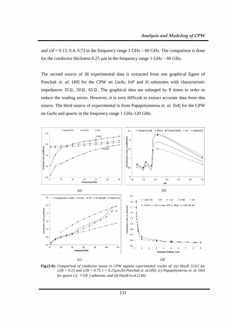
Analysis and Modeling of CPW
131
and s/d = 0.13, 0.4, 0.73 in the frequency range 1 GHz – 60 GHz. The comparison is done
for the conductor thickness 0.25 µm in the frequency range 1 GHz – 60 GHz.
The second source of 36 experimental data is extracted from one graphical figure of
Ponchak et. al. [49] for the CPW on GaAs, InP and Si substrates with characteristic
impedances 35Ω , 50Ω , 65Ω . The graphical data are enlarged by 8 times in order to
reduce the reading errors. However, it is very difficult to extract accurate data from this
source. The third source of experimental is from Papapolymerou et. al. [64] for the CPW
on GaAs and quartz in the frequency range 1 GHz-120 GHz.
(a) (b)
(c) (d)
Fig.(5.9): Comparison of conductor losses in CPW against experimental results of: (a) Haydl [131] for s/2b = 0.13 and s/2b = 0.73, t = 0.25µm,(b) Ponchak et. al.[49], (c) Papapolymerou et. al. [64] for quartz ( 8.3=rε ) substrate, and (d) Haydl et.al.[136].

Analysis and Modeling of CPW
132
Table-5.2 shows details of the CPW structures used by three groups of investigators.
Table-5.3 presents the average in four models against the experimental results. Table-5.3
also shows a summary of overall deviation and maximum deviation in three models and
two EM-simulators against the experimental results of three groups of investigators. The
present improved HK (IHK) model has better average accuracy (4.4%-5.4%) against
three groups of experimental results. The model of Ponchak et. al. has high deviation
(17.07%) against the experimental results of Haydl et. al. It has small deviation (5.52%)
only against its own experimental data that has been used for the development of their
empirical expression. The IHK model gives maximum deviation 18% for some rare
cases. The maximum deviations in HK model and PMK models are 62.5% and 26.8%
respectively. HFSS has average deviation 7.8%, maximum deviation 25.2% and Sonnet
has average deviation 10.3%, maximum deviation 33.6%. Thus the IHK model is more
accurate than any of the existing closed-form models as compared against the
experimental results from three independent sources [49, 64, 131, 136].
So far we have compared above accuracy of the IHK model against the experimental
results for the conductor thickness between 0.25 µm – 1.58 µm. However, present MMIC
technology also uses thick strip conductors in the range of 3 µm - 9 µm in order to get
high- Q planar inductors [57]. Therefore accuracy of the IHK- model for the conductor
loss of CPW with thick conductor is also examined against the results of EM-simulators.
In Fig.(5.9d), the IHK model and three EM-simulators are compared for the range 0.25
µm ≤≤ t 9 µm, against the experimental results of Haydl et. al. [136]. The % average
and % maximum deviation of the model, HFSS, Sonnet and CST w.r.t. Haydl’s results
are (4.9%, 8.8%), (5.9%, 9.7%), (5.4%, 8.6%) and (5.6%, 8.9%) respectively. The
present IHK model results are closer to experimental results as compared to the results of
EM-simulators

Analysis and Modeling of CPW
133
Table - 5.2: CPW structures
Table- 5.3: Average and overall deviations of four models and two EM-simulators
The total loss of the CPW structures is computed by adding the conductor loss and
dielectric loss together, i.e.
lengthunit/dBdcT ααα += (5.28)
The variation in Tα w.r.t. frequency in CPW, on different substrates with rε = 3.78, 9.8
and 20; s/w =0.44, h = 635 µm, tan δ = 0.002 and t = 5 µm, is shown in Fig.(5.10a). The
closed-form model for cα (IHK model) and dα (equation-(5.14)) are used for the
computation of Tα and compared against the EM- simulators within 7.4% average
deviation. Fig.(5.10b) shows the comparison of computed Tα by the model against the
EM-simulators as a function of s/(s+2w) ratio with 5.7% average deviation. For thick
S.No Sets s/2b t(µm) εr 1 Haydl [136] 0.13 0.25 InP (12.6) 2 Haydl [131] 0.4 0.25 InP (12.6) 3 Haydl [136] 0.73 0.25 InP (12.6) 4 Haydl [131] 0.13 0.5 InP (12.6) 5 Haydl [131] 0.4 0.5 InP (12.6) 6 Haydl [131] 0.73 0.5 InP (12.6) 7 Haydl [131] 0.73 1 GaAs (12.9) 8 Ponchak [49] 0.10- 0.11 1.58 InP (12.4), GaAs (12.85) 9 Papapolymerou [64] 0.28 1 Quartz (3.8), GaAs (12.85)
Model
Sl.No
1
Haydl
[136]
2
Haydl
[131]
3
Haydl
[136]
4
Haydl
[131]
5
Haydl
[131]
6
Haydl
[131]
7
Haydl
[131]
Haydl
8
Ponchak
9
Papapolymerou
Av Max Av Max Av Max
HK [ 21] 8.4 13.4 22.4 12.9 15.5 11.2 12.1 13.7 34.3 13.8 31 14.6 62.5
Wheeler[13] - - - 32.1 32.2 15.1 21 - - - - 11.7 32.6
Ponchak[49] 35.1 25 10.2 18.3 16.4 6.1 8.3 17.1 26.8 5.5 24.6 7.8 18.1
IHK 3.3 4.3 5.1 4.2 5.8 6.1 4.0 4.4 17.5 4.7 33.3 5.4 18.0
HFSS 4.0 6.1 3.1 6.1 7.9 7.2 8.0 6.1 23.1 7.4 25.2 10.1 22.0
Sonnet 5.8 9.8 13.1 6.1 10.6 12.9 6.9 9.3 27.5 10.2 33.6 11.5 22.6

Analysis and Modeling of CPW
134
conductors, the closed-form model shows close agreement with the softwares. Fig.(5.10c)
shows the variation of unloaded Q factor (Qu ) in CPW on different substrates with
rε = 3.78, 9.8 and 20; s/w =0.44 , h = 635 µm, tan δ = 0.002 and t = 5 µm in the
frequency range 0.1 GHz – 200 GHz. Fig.(5.10d) compares computation of Qu for
rε = 3.78 and 20; f = 20GHz as a function of s/(s+2w) ratio. Overall, % average and %
maximum deviation in the closed-form model against EM-simulators are 6.7% and 9%
respectively.
(a) (b)
(c) (d)
Fig.(5.10): Total loss, as a function of (a) Frequency and (b) s/(s+2w) ratio and Q factor, as a function of
(c) Frequency and (d) s/(s+2w) ratio for CPW on various substrates.

Analysis and Modeling of CPW
135
5.5 Effect of Asymmetry in Characteristics of CPW
The structures of asymmetric CPW (ACPW) shown in Fig.(5.11a) provide additional
degree of freedom to control characteristic impedance and effective permittivity. Hanna
et. al. [151], using conformal mapping method, reported analytical closed-form
expressions to compute quasi-static values of effε and Z0 of the ACPW with infinite or
finite dielectric thickness. They have shown experimental results on six asymmetric
CPWs, fabricated on an alumina substrate ( 99.r =ε and h = 0.635 mm) metalized with
gold of thickness 4 µm. Karpuz and Görür [20] have reported another analytical closed-
form expression, for the quasi-TEM parameters of ACPW using conformal mapping
technique. However, both the authors have not considered effect of conductor thickness
and dispersion in their models. Only a few publications present loss computation of
ACPW using conformal-mapping technique [48, 83]. We present below computation of
line parameters of ACPW.
(a) Structure of ACPW (b) Conductor- backed ACPW
(c) ACPW with upper shielding (d) Conductor-backed ACPW with upper shielding
Fig.(5.11): Different configurations of asymmetrical CPW (ACPW) structures

Analysis and Modeling of CPW
136
• Effective relative permittivity and Characteristic impedance
In our study, we have used the conductor thickness independent expressions for effε and
Z0 of the ACPW obtained from equations-(3.38) and (3.39) respectively:
)k(K
)k(K
)k(K
)k(K)(
'
'
reff5
5
4
412
11 −+= εε (a)
)k(K
)k(KZ
'
eff 4
40
60
επ=
(b) (5.29)
where, modulus 4k and 5k along with their complementary modulus 'k4 and 'k5 are
defined in equations-(3.33) and (3.36) respectively. However, these expressions are
modified empirically to take into account the finite strip conductor thickness and the
skin-depth penetration using equation-(5.10) and (5.13).
(a) (b)
Fig.(5.12): Comparison against experimental results of Hanna et. al. with three cases of asymmetry: (a) Effective relative permittivity and (b) Characteristic impedance Fig. (5.12a) compares effε computed by the closed-form model on the substrate with
( 99.r =ε and h = 0.635 mm) and gold conductor of thickness 4 µm. rε = 9.9 against two

Analysis and Modeling of CPW
137
EM-simulators for three cases of asymmetry i.e. w1/w2= 0.1, 1 and 2.5 for frequency
range 1 GHz - 60 GHz. The model is showing closer agreement with HFSS and has %
average and % maximum deviation of (0.89%, 2.7%) and (1.53%, 4.19%) w.r.t. HFSS
and Sonnet respectively. However the closed- form model does not account for the low
frequency dispersion due to the skin-effect penetration. The results of the model are in
between results of Sonnet and HFSS. Fig. (5.12b) compares results of the closed-form
model and simulated results of HFSS against the experimental results of Hanna et. al.
[151] for Z0. For computation of characteristic impedance, the model has average
accuracy of 1.95% and maximum deviation of 3.85% over whole frequency range. The
model and EM-simulator results are nearly identical. It can be concluded that for a given
shape ratio s/(s+w1+w2), the line asymmetry leads to decrease of its Z0 and to an increase
in effε .
• Dielectric loss
The dielectric loss of ACPW is computed using equation-(5.14) in which ),( tfeffε is
used from equation-(5.29a).
• Conductor loss
The conductor loss of ACPW is computed with the help of Wheeler’s incremental
inductance rule [13] and using the perturbation method. Equation-(5.29b) of
characteristic impedance accounts for the asymmetry in the CPW structure in Wheeler’s
method:
),t,f,h,s,w,w(Z
),t,f,h,s,w,w,(Z)t,f,h,s,w,w,(
reqeqeq
srreffc 1
1
210
2121
0 ==
=ε
δε∆εελπα
Np/m (5.30)

Analysis and Modeling of CPW
138
Holloway and Kuester have not accounted asymmetry in conductor loss computation of
CPW [21]. Our improved Holloway and Kuester (IHK) closed-form expression presented
below accounts for the asymmetry in CPW for computation of the conductor loss of
ACPW. Due to asymmetry, shown in Fig.(5.11a) the longitudinal current I and the
current density J over the strip conductors from equation-(5.16), is defined by the
following function:
( )( )( ) ( )( )( )
( )( ) )c(abab)'k(K
IA,where
)b(bxbxbxax
AJ)a(ax
xbxbxa
AJ
++=
>+−−
−=<+−−
=
21
212
212
4
22
where 2122112bbb;awb;awb;
sa +=+=+== . (5.31)
The ratio of current density (J) to the longitudinal current (I) is integrated along whole of
the strip as follows:
+
+
=
∫∫∫∫∞
+
−
+−
−−
∞− ∆
∆
∆
∆
1
2 2222
2b
a
a stripcentral
b
dlI
Jdl
I
Jdl
I
Jdl
I
Jgndlateralgndlateral
(5.32)
On integrating to the whole range, the final expression for the conductor loss of the
ACPW structure is
( )
( )
( )
( )
+++−
+
++
−+
+
+++−
+
++
−
+
++
+++−
+
−
−+
+
+++−
+
−
−+
⋅≈
∆∆
∆
∆∆
∆
∆∆
∆
∆∆
∆
α
ab
abln
bbln
ab
ab
ab
abln
bbln
ab
ab
bb
ab
abln
aln
ab
ab
ab
abln
aln
ab
ab
a
)'k(Kt,fZ
Rsmc
1
121
1
2
2
2
21
2
1
21
1
2
2
2
2
1
1
1
20
1
1
1
12
12
2
1
16
(5.33)

Analysis and Modeling of CPW
139
(a) w1/w2=1 (b) w1/w2=2
(c) w1/w2=4 (d) w1/w2 =4
Fig.(5.13): Total loss of ACPW as function of: (a)-(c) line impedance for three different values of the
asymmetry parameter w1/w2 ,and (d) conductor thickness. Fig.(5.13a) - Fig.(5.13c) compare the results for computed total loss Tα of ACPW by
IHK, Wheeler [13], HFSS, Sonnet and Ghione [48] against the SDA- based results of
Kitazawa [120] for three cases of asymmetry. The ACPW is considered on a semi-
conductor substrate with rε = 12.8, tan δ = 0.0006, f = 60 GHz, h = 100 µm, σ = 5.88 x
107 S/m and t = 3 µm. The inner spacing of two ground is maintained as b1+ b2 = 300
µm. We have computed the total loss for three cases of asymmetry i.e. w1/w2 =1, 2 and 4
by varying the line impedance from 30 Ω -130 Ω. As the b1+ b2 is maintained at 300 µm,

Analysis and Modeling of CPW
140
the slot-width becomes narrower with increase in the width of the central conductor, thus
changing the line impedance accordingly. We have also computed the loss of the
structure using HFSS and Sonnet. It is observed that with increase in asymmetry ratio
w1/w2 from 1 to 4, the loss increases. Outcome of the comparison in terms of % average
and % maximum deviation is summarized in Table-5.4. The IHK model has the highest
accuracy amongst all with % average deviation of 2.3%.
For w1/w2 = 4 and s =160 µm, Fig.(5.13d) shows variation of Tα in ACPW w.r.t.
conductor thickness in the range 0.25 µm - 9 µm. As expected, the conductor loss
decreases with increase in conductor thickness. The results of IHK, HFSS and Sonnet
follow results of Kitazawa closely with average deviation of 1.18%. Whereas results of
Wheeler’s incremental inductance formulation deviates much and it fails to compute the
loss for the conductor thickness less than the skin-depth. Otherwise, the IHK model,
HFSS and Sonnet are in close agreement with each other with % average deviation of
1.18%.
Table - 5.4: % Deviation of models against analytical results of Kitazawa [120] [Data range: t= 3 µm; f = 60 GHz; εr=12.8; tanδ=0.0006; σ=5.88x 10⁷S/m]
w2/w1
%
Deviation
IHK
Wheeler
[13]
Sonnet
HFSS
Ghione [48]
1
Av. 2.5 12.4 5.5 5.4 3.9 Max. 5.3 17.7 34.3 37.8 11.9
2
Av. 2.1 15.3 5.1 5.9 2.9
Max. 5.5 21.6 33.5 33.4 9.4
4
Av. 2.2 28.8 5.1 4.7 3.2
Max. 4.8 37.9 20.2 18.3 8.5
Overall Av. 2.3 18.9 5.6 5.4 3.3
Max. 5.6 37.9 34.3 37.8 11.9

Analysis and Modeling of CPW
141
5.6 Effect of Top Shield and Conductor Backing
The top shield is used to protect a CPW against the environment. It is also useful for the
post fabrication adjustment of the line parameters. The conductor-backed CPW provides
mechanical strength and improves the average power-handling capacity of the structure
for thin and fragile semiconductor and quartz substrates. These types of structures are
explored and used to implement a band-reject filter and end-coupled filters [60,117].
Further, upper shielding is almost always present in MMIC applications since the
conductor- backed configuration put inside a metallic enclosure offers protection from
the environment [20]. We consider three different types of configurations of ACPW,
shown in Fig.(5.11b)-(5.11d):
• Conductor – backed ACPW (CBACPW)
• ACPW with upper shielding (ACPWUS)
• Conductor-backed ACPW with upper shielding (CBACPWUS)
The thickness of the substrate, having relative permittivity rε , is h and the top shield is
located at the height h1. The medium between the strip conductors and the top shield is
air with 1r =ε . Karpuz et. al. [20] reported static analytic expressions for effε and Z0 of
the CBACPW, ACPWUS and CBACPWUS using the conformal mapping techniques.
They have ignored conductor thickness. Their expressions are summarized below:
• CBACPW:
′+
′
′−+=
)k(K
)k(K
)k(K
)k(K)k(K
)k(K
)( reff
6
6
4
4
6
6
11 εε
(a)
)k(K
)k(K
)k(K
)k(KZ
eff
6
6
4
40
1120
′+
′ε
π= (b) (5.34)

Analysis and Modeling of CPW
142
• ACPWUS:
′+
′
′−+=
)k(K
)k(K
)k(K
)k(K
)k(K
)k(K
)( reff
7
7
4
4
5
5
11 εε (a)
)k(K
)k(K
)k(K
)k(KZ
eff
7
7
4
40
1120
′+
′
=ε
π (b) (5.35)
• CBACPWUS:
effε
′+
′
′−+=
)k(K
)k(K
)k(K
)k(K
)k(K
)k(K
)( r
7
7
6
6
6
6
11 ε (a)
)k(K
)k(K
)k(K
)k(KZ
eff
7
7
6
60
1120
′+
′ε
π= (b) (5.36)
where modulus 4k and 5k along with their complementary modulus 'k4 and 'k5 are
defined in equations-(3.33) and (3.36) respectively, and modulus k6 and k7 are given
below
[ ]
[ ] [ ])sw()sw(
s/)ww(k
''''
'''
21
21
11
16
++
++= (a) 2
6'6 k1k −=
(b) (5.37)
[ ]
[ ] [ ])sw()sw(
s/)ww(k
''''''''
''''''
21
21
11
17
++
++= (a) 2
77 1 kk' −= (b) (5.38)
with
( )( )
( ))c(eew
)b(eew
)a(ees
h/wh/ws'
h/wh/ws'
h/sh/s'
−=
−=
−=
ππ+−
ππ+−
ππ−
1
1
1
22
11
222
221
2
( )
( ))f(eew
)e(eew
)d(ees
h/wh/ws''
h/wh/ws''
h/sh/s''
−=
−=
−=
ππ+−
ππ+−
ππ−
1
1
1
1212
1111
11
222
221
2
(5.39)

Analysis and Modeling of CPW
143
In case asymmetry ratio (w1/w2) is 1, the above mentioned equations can be used to study
the effect of conductor backing and upper shielding on symmetric CPW as well.
The SLR formulation (discussed in section-4.4.2) is used to extend the closed-form
models for ACPW to compute line parameters of CBACPW, ACPWUS and
CBACPWUS. Over the equivalent single-layer substrate with an equivalent relative
permittivity ( reqε ), equivalent loss tangent ( eqtan δ ) and equivalent substrate thickness
( eqh ), the empirical expressions from equation-(5.10) and (5.13) along with equations-
(5.34) - (5.36) are used to compute ),( tfeffε , )t,f(Z0 , dα and cα of all the three
structures.
Fig. (5.14) – (5.16) shows comparison of computed line parameters of all the three
structures - CBACPW, ACPWUS and CBACPWUS respectively, against two EM-
simulators – HFSS and Sonnet. In Fig.(5.14a) and (5.14b), effε and Z0 of CBACPW for
G/h = 1, 2 and 4, where, shown in Fig.(5.11b), G is ground-to-ground width (G = w1 + w2
+ s); asymmetry ratio w1/w2 = 0.4, rε = 2.5, t = 4 µm, h = 635 µm for frequency range 1
GHz - 60 GHz are shown. In Fig.(5.14a), computed effε by the model shows better
agreement with Sonnet, while results of HFSS are marginally on the higher side. Like
EM-simulators, the present model shows low frequency dispersion. In Fig.(5.14b),
computed Z0 by the model is in close agreement with both the EM simulators, having
almost identical results except for f <10 GHz. The results of simulators show increase in
characteristic impedance as it is based on power – voltage definition. However model
shows decrease in characteristic impedance as the model uses V-I definition. It results
into deviation in the results. The computation of effε and Z0 by the model has % average
and % maximum deviation of (2.17%, 5.53%) and (3.07%, 5.83%) respectively against
both the EM simulators. It is observed that both effε and Z0 increase with increase in G/h
ratio from 1 to 4.
Analysis and Modeling of CPW
144
(a) (b)
(c) (d)
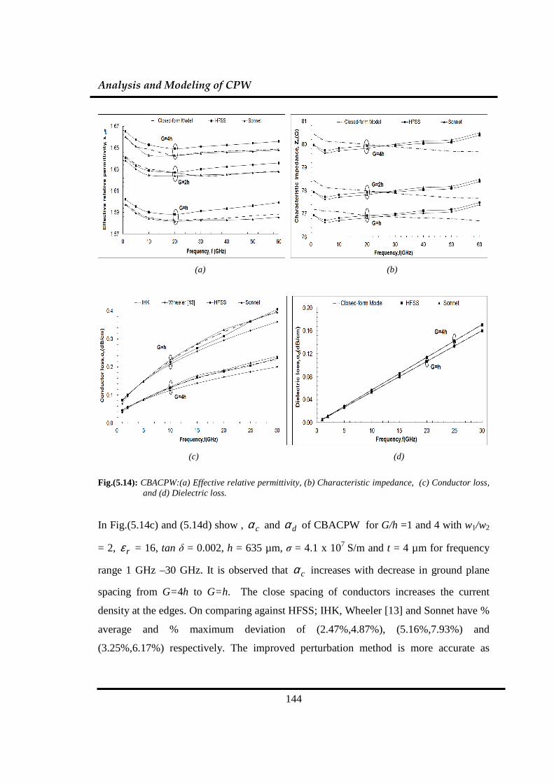
Fig.(5.14): CBACPW:(a) Effective relative permittivity, (b) Characteristic impedance, (c) Conductor loss,
and (d) Dielectric loss.
In Fig.(5.14c) and (5.14d) show , cα and dα of CBACPW for G/h =1 and 4 with w1/w2
= 2, rε = 16, tan δ = 0.002, h = 635 µm, σ = 4.1 x 10⁷ S/m and t = 4 µm for frequency
range 1 GHz –30 GHz. It is observed that cα increases with decrease in ground plane
spacing from G=4h to G=h. The close spacing of conductors increases the current
density at the edges. On comparing against HFSS; IHK, Wheeler [13] and Sonnet have %
average and % maximum deviation of (2.47%,4.87%), (5.16%,7.93%) and
(3.25%,6.17%) respectively. The improved perturbation method is more accurate as

Analysis and Modeling of CPW
145
compared to Wheeler’s model. It is observed that dα increases as G/h ratio increases
from 1 to 4, as shown in Fig.(5.14d). The increase in separation between conductors for
the conductor-backed CPW permits more concentration of electric field in the lossy
substrate. It increases the dielectric loss. The model is in close agreement with both the
EM simulators with % average deviation of only 0.13%.
(a) (b)
(c) (d)
Fig.(5.15): ACPWUS:(a) Effective relative permittivity, (b) Characteristic impedance, (c) Conductor loss,
and (d) Dielectric loss.
Fig.(5.15a) and (5.15b) show effε and Z0 of the asymmetric CPW with upper shield

Analysis and Modeling of CPW
146
(ACPWUS). The structure is shown in Fig.(5.11c). The results are presented for G/h = 1
and 4;. h1/h = 2 and 5 with rε =2.5, t = 4 µm, h = 635 µm for frequency range 1 GHz –
60 GHz. The computation of effε and Z0 by the model has % average and % maximum
deviation of (4.14%, 6.75%) and (4.26%,6.83%) respectively against both the EM
simulators. Both effε and Z0 increase with increasing h1/h ratio, whereas effε decreases
and Z0 increases with increasing G/h ratio.
In Fig.(5.15c) and (5.15d), cα and dα of ACPWUS for G/h = 2 and 4 ; h1/h = 2 and 10
with w1/w2 = 2, rε = 16, tan δ = 0.002, h = 635 µm, σ = 4.1 x 10⁷ S/m, t = 4 µm and
frequency range 1 GHz – 30 GHz, are shown. It is observed that cα increases when
upper shielding is nearer to the substrate and it increases as G/h ratio decreases from 4 to
2, as shown in Fig.(5.15c). The IHK, Wheeler [13] and Sonnet have % average and %
maximum deviation of (4.16%,6.93%), (5.98%,8.9%) and (2.89%,5.96%) respectively
w.r.t. HFSS. It is also observed that dα decreases as h1/h ratio decreases from 10 to 2
and it increases as G/h ratio increases from 2 to 4, as shown in Fig.(5.15d). The closed-
form model has 1.8% average deviation against both the EM simulators.
In Fig.(5.16a) and (5.16b), effε and Z0 of CBACPWSH for G/h = 1 and 4;. h1/h = 2 and 5
with rε =2.5, t = 4 µm, h = 750 µm for frequency range 1 GHz – 60 GHz, are shown.
The computation of effε and Z0 by the model has % average and % maximum deviation
of (2.4%,5.82%) and (2.84%,3.65%) respectively against both the EM simulators. It is
observed that both effε and Z0 increases with increasing h1/h ratio and G/h ratio.
In Fig.(5.16c) and (5.16d), cα and dα of CBACPWSH for G/h = 1 and 2 ; h1/h = 2 and
10 with w1/w2 = 2, rε = 16, tan δ = 0.002, h = 750 µm, σ = 4.1 x 10⁷ S/m, t = 4 µm and
frequency range 1 GHz – 30 GHz, are shown. It is observed that the presence of both

Analysis and Modeling of CPW
147
conductor backing and upper shielding increases cα when G/h ratio is nearer to 1 and
height of upper shielding is nearer to the substrate. The IHK, Wheeler [13] and Sonnet
have % average and % maximum deviation of (2.68%,4.71%), (4.11%,7.57%) and
(3.19%,6.9%) respectively w.r.t. HFSS. It is observed that dα decreases when h1/h ratio
decreases from 10 to 2 and when G/h ratio increases from 1 to 2. The closed-form model
has 0.75% average deviation against both the EM simulators.
(a) (b)
(c) (d)
Fig.(5.16): CBACPWUS: (a) Effective relative permittivity, (b) Characteristic impedance, (c) Conductor loss, and (d) Dielectric loss.

Analysis and Modeling of CPW
148
5.7 Closed-form Dispersion and Loss Models for Multilayer CPW
The combined strength of the CPW and multilayer MMIC technology provides an
attractive field for the design of compact low cost MMICs for affordable wireless
communications [60]. The cross-sectional view of a CPW on multilayer dielectric
substrates is shown in Fig.(5.17).
(a): Six layered CPW
(b): Two layered composite CPW (c): Thee layered composite CPW
Fig.(5.17): Schematic of a multilayered CPW structure. Svačina [66] has applied conformal mapping technique to obtain general expressions for
capacitance of multilayer unshielded and without conductor-backed CPW. Others have
adopted these existing conformal mapping results for the multilayer cases. However their
Analysis and Modeling of CPW
149
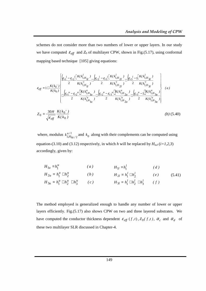
schemes do not consider more than two numbers of lower or upper layers. In our study
we have computed effε and Z0 of multilayer CPW, shown in Fig.(5.17), using conformal
mapping based technique [105] giving equations:
( ) ( ) ( )
( ) ( ) ( ))a(
)k(K
)k(K
)k(K
)k(K
)k(K
)k(K
)k(K
)k(K
)k(K
)k(K
)k(K
)k(K
)k(K
)'k(K
u'H,
uH,u
ru'H,
uH,u
ru
ru'H,
uH,u
ru
r
l'H,
lH,l
rl'H,
lH,l
rl
rl'H,
lH,l
rl
r
eff
u
u
u
u
u
u
l
l
l
l
l
l
−+−+−+
−+−+−
+=
3
3
2
2
1
1
3
3
2
2
1
1
1
13
1
132
1
121
1
13
1
132
1
121
0
0
2
1
22
2
1
22
1
εεεεε
εεεεε
ε
)k(K
)'k(KZ
eff 0
00
30
επ= (b) (5.40)
where, modulus l/uH, l/iu
k1and 0k along with their complements can be computed using
equation-(3.10) and (3.12) respectively, in which h will be replaced by Hiu/l (i=1,2,3)
accordingly, given by:
)c(hhhH
)b(hhH
)a(hH
uuuu
uuu
uu
3213
212
11
++=
+=
=
)f(hhhH
)e(hhH
)d(hH
llll
lll
ll
3213
212
11
++=
+=
=
(5.41)
The method employed is generalized enough to handle any number of lower or upper
layers efficiently. Fig.(5.17) also shows CPW on two and three layered substrates. We
have computed the conductor thickness dependent ),( tfeffε , )t,f(Z0 , cα and dα of
these two multilayer SLR discussed in Chapter-4.

Analysis and Modeling of CPW
150
( ) ( ) ( )
( ) ( )
( ) ( ) )(
)(
)(
2
1
)(
)(
2
1
)(
)(
2)(
)(
2
)(
)'(1:
)()(
)(
2
1
)(
)(
2
1
)(
)(
2)(
)'(1:
',1
,10',1
,13
',1
,132',1
,121
0
0
',1
,10',1
,12',1
,121
0
0
1
1
3
3
2
2
1
1
1
1
2
2
1
1
b
kK
kK
kK
kK
kK
kK
kK
kK
kK
kKLayerThree
akK
kK
kK
kK
kK
kK
kK
kKlayerTwo
uH
uH
u
lH
lH
lr
lH
lH
lr
lr
lH
lH
lr
lr
eff
uH
uH
u
lH
lH
lr
lH
lH
lr
lr
eff
u
u
l
l
l
l
l
l
u
u
l
l
l
l
−+−+
−+−
+=
−+−+−+=
εε
εεεε
ε
εεεεε
(5.42)
The dispersive effective relative permittivity, characteristic impedance and losses are
computed as follows:
• Effective relative permittivity
[ ]
=−
+
=×−+=×=
−
)k(K
)k(K
)k(K
)k(KS,factoreffectSkinwhere
)f/f(m
)t,f(S)t,f(S),t,f(
't,
t,
,
',
rTE
effreqeffeff
0
0
0
0
2
1
00
δ
δ
εεεδε
(a)
• Characteristic impedance
( )Stf
tfZeff
1
),(
30,0 ×=
επ
(b)
• Wheeler’s incremental inductance rule
),t,f,h,s,w(Z
),t,f,h,s,w,(Z)t,f,h,s,w,(
.
reqeqeqeq
seqreqeqreqeffc 1
12927
00 =
==
εδε∆
εελ
α
dB/m (c)
• Improved Holloway and Kuester (IHK)
( )
+−
+−+
−+
+−⋅
−=
bc
bc
ab
abbln
bac
ac
ab
abaln
a)ab)(k(Kt,fZ
bRsmc ∆∆
α 2121
16 2220
2 Np/m (d)

Analysis and Modeling of CPW
151
(a) (b)
(c) (d)
Fig.(5.18): Two layered composite substrate CPW: (a) Effective relative permittivity, (b) Characteristic
impedance, (c) Conductor loss, and (d) Dielectric loss.
• Dielectric loss
01
12927
λδ
ε
ε
ε
εα eq
req
eff
eff
reqd
tan)t,f(
)t,f(.
−
−= dB/m (e) (5.43)
where eqh is the total substrate thickness between strip conductors and bottom layer of
the multilayer substrate. reqε and eqtanδ of the equivalent single-layer substrate CPW

Analysis and Modeling of CPW
152
are obtained from equation-(4.28). The dielectric loss and conductor loss of multilayer
CPW had been computed by Verma et. al. [13-14] using SLR technique.
(a) (b)
(c) (d) Fig.(5.19): Three layered composite substrate CPW: (a) Effective relative permittivity, (b) Characteristic
impedance, (c) Conductor loss, and (d) Dielectric loss.
Fig. (5.18a) – (5.18d) show comparison and validity of SLR-based computed line
parameters of two layered composite substrate CPW against results from experiment,

Analysis and Modeling of CPW
153
SDA and softwares, for different line structures. Fig. (5.19a) – (5.19d) show such
comparisons for three layered composite substrate CPW. The computed effε and Z0 by
the model has average deviation of 1.63% and 4.6% respectively, against SDA-based
results of Bedair et.al. [110]. The computed effε and Z0 by the model has average and
maximum deviation of (1.8%, 3.7%) and (5.1%, 12%) respectively against both the EM
simulators for frequency range 1 GHz –65 GHz. The variation in cα and dα of
multilayer CPW are shown in Fig.(5.18) and Fig. (5.19). Papapolymerou et. al. [64]
results of cα for frequency range 2 GHz – 118 GHz on polyimide Pyralin PI2545
( rε =3.5) is taken with two GaAs wafers, in order to get a thickness of 3 µm. The results
for both closed-form models and EM-simulators are compared against this experimental
result.
Overall, the average and maximum deviations in IHK, Wheeler, HFSS and Sonnet are
(3.4%,9.8%), (4.7%,10.1%), (5.3%,9.8%) and (3.8%,8.6%) respectively. The computed
dα by the model is in close agreement with both the EM simulators and MoM based
LINPAR, for frequency range 1 GHz – 60 GHz, with % average deviation of 4.6%.
5.8 Closed-form Dispersion and Loss Models for Non-Planar CPW
There is a demand for non- planar CPW i.e. CPW on elliptical surface (ECPW) and CPW
on cylindrical surface (CCPW) in order to produce compact devices applicable to aircraft,
missiles and mobile communication. Such structures are needed to feed wrapped around
printed antennas on different geometric surfaces [54, 84-85, 90]. To date, many authors
[19, 52, 55, 85, 90, 130] have investigated the electrical parameters of ECPW and CCPW
using full-wave approach incorporating a moment-method calculation and conformal
mapping technique. However, effect of conductor thickness and dispersion on line

Analysis and Modeling of CPW
154
parameters of non-planar CPW has not been investigated yet using closed-form
expressions.
In this section, we will present the CAD oriented closed-form models for the line
parameters of different configurations of single-layered and multilayered non-planar
CPW, shown in Fig.(5.20) and (5.23). The available static closed-form models are
modified empirically, to take into account the finite strip conductor thickness and
dispersion on the circular and elliptical cylindrical surfaces, by adopting the expressions
used for the planar single-layered and multilayered CPW.
5.8.1 Single-Layer Case
The four configurations of non-planar CPW with finite ground plane width – on elliptical,
circular, semi- ellipsoidal and semi-circular cylindrical surfaces, are shown in Fig.(5.20).
The structural parameters of the SC - transformed ECPW/ CCPW into the corresponding
planar CPW are given by equation-(3.54):
)iv(ba
balnt)iii(
ba
balnh)ii(w)i(s
22
33
11
222++
=++
=−== ψθΨ (5.44)
The detailed definition of the above mentioned parameters are given in Chapter-3.
• Effective relative permittivity and Characteristic impedance
We have used available static expressions for effε and Z0 of the non-planar CPW
without conductor thickness to compute the strip conductor thickness dependent
dispersive effε and Z0 of the non-planar CPW. The static expressions for effε and Z0 of
the non-planar CPW obtained from equations-(3.48) and (3.49) are given below

Analysis and Modeling of CPW
155
)'k(K
)k(K
)k(K
)'k(K
2
11
1
1
0
0reff
−+=
εε (a)
)k(K
)'k(K30Z
0
0
eff0 ε
π=
(b) (5.45)
where, modulus 0k and 1k along with their complementary modulus 'k0 and 'k1 for finite
ground plane widths ( )θπ 22 − and( )θπ 2− , are obtained from equations - (3.42) -
(3.44) and equations - (3.55) - (3.56) respectively.
(a) (b)
(c) (d)
Fig.(5.20): CPW with finite ground plane on the curved surfaces: (a) ECPW, (b) CCPW, (c) SECPW and (d) SCCPW.
In order to account the strip conductor thickness for these line structures, we have to
modify equation- (5.3) to equation-(5.7) by using equation-(5.44). The equivalent slot
width ( eqθ ) and equivalent strip width (eqψ ) for the ECPW / CCPW are given as

Analysis and Modeling of CPW
156
( ))iii(
ba
baln
lnba
baln,where
)ii(),i(
r
eqeq
++−+
++=
−−=+=
22
3322
33 81
2
1
2
ψθππε
ψ∆
ψ∆ψθθψ∆ψψ
(5.46)
The modulus 0k and 1k are modified into t,0k and
t,1k along with their complementary
modulus, in which ψ and θ is replaced by eqψ and eqθ respectively. The above
equation - (5.46) can be inserted in equations - (5.10) and (5.13) to compute the
conductor thickness and frequency dependent ),( tfeffε and )t,f(Z0 of the ECPW and
CCPW lines.
• Dielectric and Conductor losses
The dielectric loss dα is computed by using equation-(5.14) in which the frequency and
conductor thickness dependent ),( tfeffε of ECPW and CCPW are used. Both
Wheeler’s incremental inductance formulation and perturbation method i.e. IHK model
are used to compute the conductor loss cα
of the non-planar CPW. Wheeler’s
incremental inductance formulation [13] is modified using equation-(5.44):
( )( )
=
++
++
++
++−=
++
++−=
1
21
2
22
33
11
220
22
33
11
22
22
33
11
22
0reqeq
sr
reffc
,ba
baln,f,
ba
baln,,Z
,ba
baln,f,
ba
baln,,,Z
ba
baln,f,
ba
baln,,,
εψθ
δψψθε∆ψψθεε
λπα
Np/m
(5.47)
Then IHK model for ECPW/CCPW with ground plane width ( )θπ 22 − is obtained by
using equation – (5.44) with equation – (5.22):

Analysis and Modeling of CPW
157
( )
+−
+−+
−+
+−
−=
θπθπ
Ψθψθ
∆θ
θψπψπ
Ψθψθ
∆Ψ
ΨΨθθα 2121
16 2220
2
lnln))(k(Kt,fZ
Rsmc Np/m (5.48)
When π is replaced by 2π in the above equation, IHK model for non-planar CPW with
ground plane width ( )θπ 2− is obtained.
We have tested the accuracy of the closed-form models developed for propagation
characteristics of non-planar CPW, for both elliptical/circular i.e. ( )θπ 22 − and semi-
elliptical/circular i.e. ( )θπ 2− ground plane width, against the results obtained from EM-
simulators- HFSS and CST, as shown in Fig.(5.21) and Fig.(5.22). Fig.(5.21) presents
comparisons of performances of CPW on the circular and semi-circular cylindrical
surfaces in respect of effective relative permittivity, characteristic impedance and losses.
Fig.(5.22) presents such comparisons for the CPW on the elliptical and semi- ellipsoidal
cylindrical surfaces. The results are obtained over the frequency range, 1 GHz – 60 GHz.
For simulation, we have taken the substrate with rε = 2.5, θ = 40°, ψ = 25°, h = 500 µm
and t = 3 µm. For ECPW, the ellipticity c = 0.7 is considered. With increase in the
ellipticity and decrease in the ground width, there is increase in effε ; whereas with
decrease in both ellipticity and ground width, Z0 increases.
We note that effective relative permittivity increases for the semi- circular and semi-
ellipsoidal CPW as compared against the CPW on the circular and elliptical surfaces. The
characteristic impedances of semi - circular and semi- ellipsoidal cases are also higher as
compared to the CPW on the circular and elliptical surfaces. The losses are almost
identical for both the cases. The closed-form model follows closely the results of both
HFSS and CST with average deviation of 2.3%. The nature of dispersion is identical for
both cases. The results are summarized in Table- (5.5).

Analysis and Modeling of CPW
158
(a) (b)
(c) (d)
(e) (f)
Fig.(5.21): Comparison of different line parameters of non-planar CPW on circular and semi-circular
surfaces.

Analysis and Modeling of CPW
159
(a) (b)
(c) (d)
(e) (f)
Fig.(5.22): Comparison of different line parameters of non-planar CPW on elliptical and semi-ellipsoidal
surfaces.

Analysis and Modeling of CPW
160
Fig.(5.21) and Fig.(5.22) also show the effect of conductor thickness on effε and Z0 of
CCPW and ECPW with varying dimensional parameter ratio ψ/θ for rε =9.8, ψ = 25°,
h = 500 µm, c = 0.5 and f = 30 GHz .The two conductor thicknesses t = 3 µm and 6 µm
are used in the investigation. Both effε and Z0 decreases with increase in the conductor
thickness.
Table - 5.5: % Change in characteristics of models against simulators on non-planar CPW with different ground-plane widths
(a): % change in characteristics of semi-ellipsoidal CPW over elliptical CPW.
Characteristics
Closed-form Model HFSS CST
% av.
change
% max.
change
% av.
change
% max.
change
% av.
change
% max.
change
Increase in Effective relative permittivity
1.6
1.8
3.1
3.8 2.6 3.1
Increase in Characteristic impedance
7.3 10.5 4.8 5.2 5.1 5.7
Decrease in Total loss
2.6 4.3 1.6 2.3 1.8 2.4
(b): % change in characteristics of semi-circular CPW over circular cylindrical CPW.
Characteristics Closed-form Model HFSS CST
% av.
change
% max.
change
% av.
change
% max.
change
% av.
change
% max.
change
Increase in Effective relative permittivity
6.3
6.5
2.3
2.6 3.3 3.5
Increase in Characteristic impedance
4.4 4.7 4.7 5.1 5.01 5.3
Decrease in Total loss
2.8 4.9 1.7 2.5 1.9 2.7

Analysis and Modeling of CPW
161
The total losses Tα are compared for non-planar CPW with both cases of finite ground
plane between frequency ranges 1 GHz – 60 GHz. We have taken t = 3µm, θ = 40°, ψ =
35°, c = 0.7, h = 500 µm, tan δ = 0.0015 and σ = 4.1 x 10⁷ S/m on substrate with rε =
12.9. On comparison, the closed-form model # 1 (= Wheeler + dα ) and closed-form
model # 2 (= IHK + dα ) have average and maximum deviation of (7.4%, 15.6%) and
(4.7%, 16.3%) respectively against both the EM-simulators, excluding results at 1 GHz
due to large deviations. The closed-form model # 2 is in close agreement with HFSS at
higher frequencies.
Fig.(5.21) and Fig.(5.22) further compare cα of the structures computed by Wheeler and
IHK for rε =12.9, θ = 28°, ψ = 25°, f = 60 GHz, h = 500 µm, σ = 3 x10⁷ S/m with
conductor thickness range 0.25 µm – 9 µm. Both the models are in close agreement with
HFSS. The average and maximum deviation of Wheeler and IHK against results of Duyar
et. al. [84] are (5.8%, 9.6%) and (4.4%, 14.4%) respectively.
5.8.2 Multilayer Case
In this section, we have extended the improved closed-form models for the line
parameters of single-layered, equations-(5.45)-(5.48), to multilayer non-planar CPW by
applying SLR technique and using equation-(5.43). The SLR is presented in Chapter-4.
The structural parameters of multilayer structure obtained from SC-transformation
(discussed in Chapter-3) are:
)vi(
ba
balnh)v(
ba
balnh)iv(
ba
balnh
)iii(ba
balnt)ii(w)i(s
33
553
11
332
22
331
33
442
++
=++
=++
=
++=−== ψθΨ
(5.49)

Analysis and Modeling of CPW
162
(a) (b)
(c) (d)
Fig.(5.23): Multilayer CPW with finite ground plane on the curved surfaces: (a) MECPW, (b) MCCPW,
(c) MSECPW and (d) MSCCPW.
For the sake of convenience, we have considered upto three layers only, as shown in
Fig.(5.23). The partial capacitance technique is used for computation of effε and Z0 of
the multilayer non-planar CPW. The expressions are summarized below and other details
are given in Chapter-3:
)'k(K
)k(K
)k(K
)'k(K
2
1
)'k(K
)k(K
)k(K
)'k(K
2
1
)'k(K
)k(K
)k(K
)'k(K
21
3
3
0
03r
2
2
0
02r
1
1
0
02r1reff
−+
−+
−+=
εεεεε
(a)
)k(K
)'k(K30Z
0
0
eff0 ε
π= (b) (5.50)
where modulus 0k and ki (i=1,2,3) along with their complements can be computed using
equation-(3.42) and (3.44) respectively for finite ground plane widths ( )θπ 22 −
and( )θπ 2− . The parameter H in equation–(3.45) is replaced by hi (i=1,2,3) accordingly.

Analysis and Modeling of CPW
163
(a) (b)
(c)
Fig.(5.24): Multilayer non-planar CPW: (a) Effective relative permittivity, (b) Characteristic impedance, and (c) Total loss.
Fig. (5.24) shows comparison and validity of SLR-based computed line parameters of
multilayer non-planar CPW with 1rε =3.8, 2rε =12.9, 3rε = 1, θ = 28°and ψ = 25° against
EM-simulators for frequency range 1 GHz – 60 GHz. The computation of effε and Z0 by
the model has average and maximum deviation of (4.7%, 10.8%) and (5.4%,8.3%)
respectively against both the EM simulators. Fig.(5.24) also shows the variation in Tα
of multilayer non-planar CPW for two conductor thicknesses t = 0.5 µm and 3 µm with
finite ground plane width ( )θπ 22 − . The average and maximum deviation of closed-

Analysis and Modeling of CPW
164
form model #1 and closed-form model #2 against EM-simulators are (8.5%, 19.8%) and
(5.3%,17.4%) respectively. Outcome of the comparison in terms of % average and %
maximum deviation is summarized in Table-5.6 for different multilayer configurations.
The closed-form model #2 is used for the computation of total loss.
Table - 5.6: % Deviation of models against simulators on different dielectric interfaces
[Data range: t =0.25 µm - 9 µm; f = 1 GHz - 60 GHz; θ = 28°; ψ = 25°; εr3=1; h3=500 µm; σ=4.1x 10⁷S/m]
5.9 Circuit Model of CPW
We have presented models to compute dispersive effective relative permittivity,
characteristic impedance, dielectric loss and conductor loss of CPW, CPS and slotline
structures - both planar and non-planar structures, on single-layer substrates and also on
multilayer substrates. The dispersion at low frequency, due to field penetration, has also
been accounted in the modeling. However, we know that losses have influence on the
propagation parameter and to some extent the propagation parameter also influence the
loss computation. Moreover, a lossy line has complex characteristic impedance. This
information is missing in our modeling presented so far. These missing information can
be computed with the help of R (f ), L (f ), C (f ), and G (f ) circuit model of any of these
line on assumption that they support quasi-TEM mode of propagation. We can extract
R (f ), L (f ), C (f ), and G (f ) from models of dispersive effective relative permittivity,
characteristic impedance, dielectric loss and conductor loss of transmission lines
Model
2rε = 20, 1rε = 10;h1=h2=635 µm; tanδ1=0.0015; tanδ2=0.0002
2rε = 12.9, 1rε = 10;h1=h2=635 µm; tanδ1=0.0015; tanδ2=0.002
effε Z0(Ω) Tα (dB/cm) effε Z0(Ω) Tα (dB/cm)
Av. Max. Av. Max. Av. Max. Av. Max. Av. Max. Av. Max. HFSS 3.6 11.2 4.9 8.8 4.2 15.1 4.5 12.5 5.6 8.1 4.6 13.1 CST 4.2 15.4 6.2 11.6 5.4 17.2 4.7 13.6 6.1 10.3 5.9 15.2

Analysis and Modeling of CPW
165
discussed so far. It discussed in Chapter-2. Chapter-2 also presents method to extract
these primary line parameters from the S-parameters obtained using the EM-simulators.
In this section, we first extract the primary and secondary line parameters of the CPW
using closed-form models. We compare accuracy of our parameters extraction against the
extracted line parameters using EM-simulators- HFSS, Sonnet, CST and MOM-based
software LINPAR. We have taken 0.01 GHz – 10 GHz frequency range and the CPW is
considered on the substrate with rε = 9.8, s = 45 µm, w =50 µm, h =165 µm and t =1
µm. The extracted frequency dependent RLCG line parameters are shown and compared
in Fig.(5.25).
(a) (b)
(c) (d)
Fig.(5.25): Extraction of RLCG parameters of lossy planar CPW using circuit model and EM-simulators.

Analysis and Modeling of CPW
166
The line resistance R, presented in Fig.(5.25a) shows increase with frequency and at low
frequencies resistance R, approaches a constant. As frequency increases, the skin-depth
becomes smaller than the conductor thickness and surface resistance increases as the
square-root of frequency. The results obtained from circuit model are in between the
results of HFSS and CST and are comparably closer to CST and Sonnet. The results of
LINPAR have more deviations from the EM-simulators. The line inductance L, presented
in Fig.(5.25b), shows decrease in its value with increase in frequency from 0.01 GHz to 1
GHz. It is due to decrease in the internal inductance of the CPW. Above 1 GHz change in
line inductance is insignificant. The results of the circuit model follow results of EM-
simulators closely, closer to Sonnet.
The line capacitance C, presented in Fig.(5.25c), also shows decrease in its value with
increase in frequency from 0.01 GHz to 10 GHz. However decrease is faster in the
frequency range from 0.01 GHz to 0.1 GHz and then decrease is slower. The circuit
model closely follows results of HFSS and Sonnet. It follows physical behavior of a
capacitor. We have taken both relative permittivity and loss-tangent constant of substrate
material frequency independent which is not correct from Krammer - Kronig point of
view. Thus our circuit model is non-causal. The results of circuit model and EM-
simulators, presented in Fig.(5.25d), show increase in line conductance G with frequency.
The circuit model closely follows EM-simulators.
Finally we obtain frequency dependent effective relative permittivity, characteristic
impedance - real and imaginary parts, and total loss from the RLCG parameters. These
results obtained from the circuit models are presented in Fig.(5.26) and compared against
the results of EM-simulators. The results of circuit model follow results of EM-
simulators; whereas results of our previous closed-form individual models do not follow
simulators, especially at lower end of frequency inspite of our accounting for the internal
inductance effect. It is true for all the parameters - effective relative permittivity, losses
and characteristic impedance.

Analysis and Modeling of CPW
167
(a) (b)
(c) (d)
Fig.(5.26): Comparison of circuit model, closed-form model against EM-simulators for line parameters of
lossy planar CPW in respect of )t,f(effε , ( )t,fTα , ))t,f(*Z(Re 0 and ))t,f(*Z(Im 0 .
Table-5.7 consolidates the comparison of the models against HFSS for line parameters of
CPW on the alumina substrate. All the EM-simulators are within average deviation of
1.8% amongst themselves while LINPAR has deviation w.r.t. the simulators with 5.2%
average deviation. The circuit model accurately predicts and improves the dispersive
nature of the CPW at the lower frequency range for computation of ),( tfeffε , ),(0 tfZ
and )t,f(Tα with average and maximum deviation of (3.6%, 7.5%), (2.3%, 4.5%) and

Analysis and Modeling of CPW
168
(2.1%, 5.2%) respectively. The circuit model is applicable to all the line structures
presented in this chapter. However for sake of brevity, we are not presenting the results.
Table - 5.7: % Deviation of models against HFSS [Data range: t =1 µm; f = 0.01 GHz - 10 GHz; εr=9.8; tanδ=0.0002; σ=4.1x 10⁷S/m]
Model
effε Z0 (Ω) Tα (Np/cm)
Av. Max. Av. Max. Av. Max. LINPAR 5.8 17.2 5.1 8.2 4.3 7.4 Sonnet 2.2 5.4 1.2 3.2 1.3 4.1 CST 2.5 5.8 1.6 2.8 1.8 5.6
Closed-form Model 9.6 51.8 7.7 25.1 6.3 11.3 Circuit Model 3.6 7.5 2.3 4.5 2.1 5.2