Chapter 4 Register Transfer and Micro -operations.
50
Chapter 4 Register Transfer and Micro - operations
-
Upload
prudence-carter -
Category
Documents
-
view
299 -
download
8
Transcript of Chapter 4 Register Transfer and Micro -operations.
Chapter 4 Register Transfer and Micro -operations
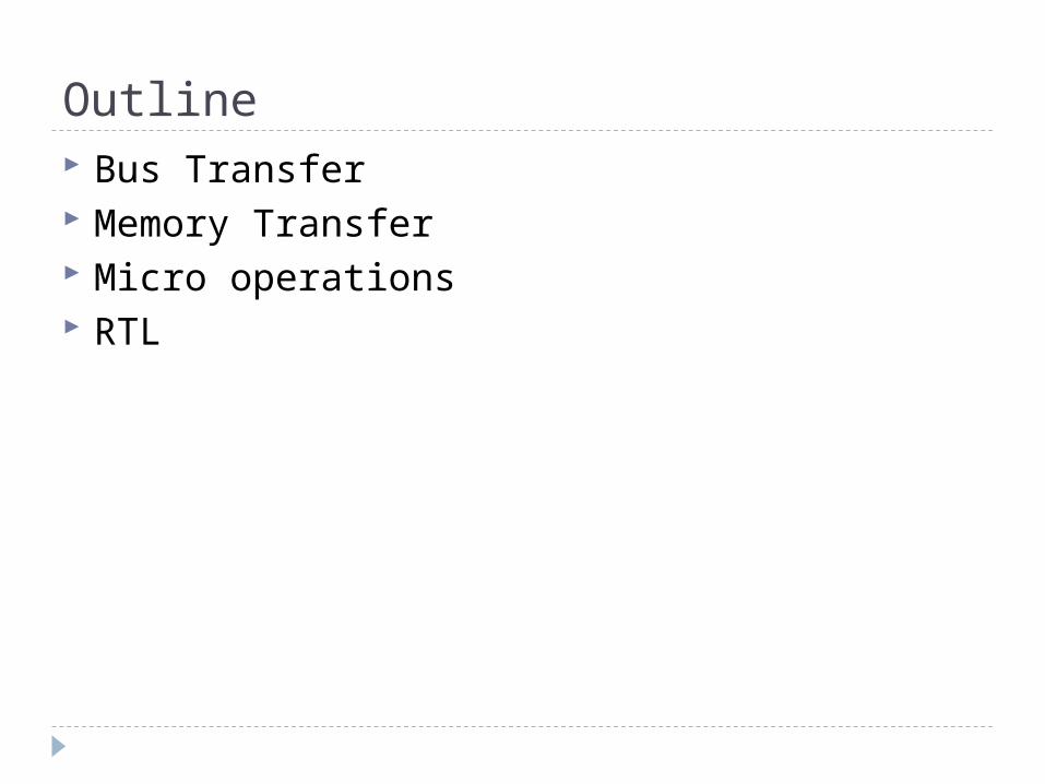
Outline Bus Transfer Memory Transfer Micro operations RTL
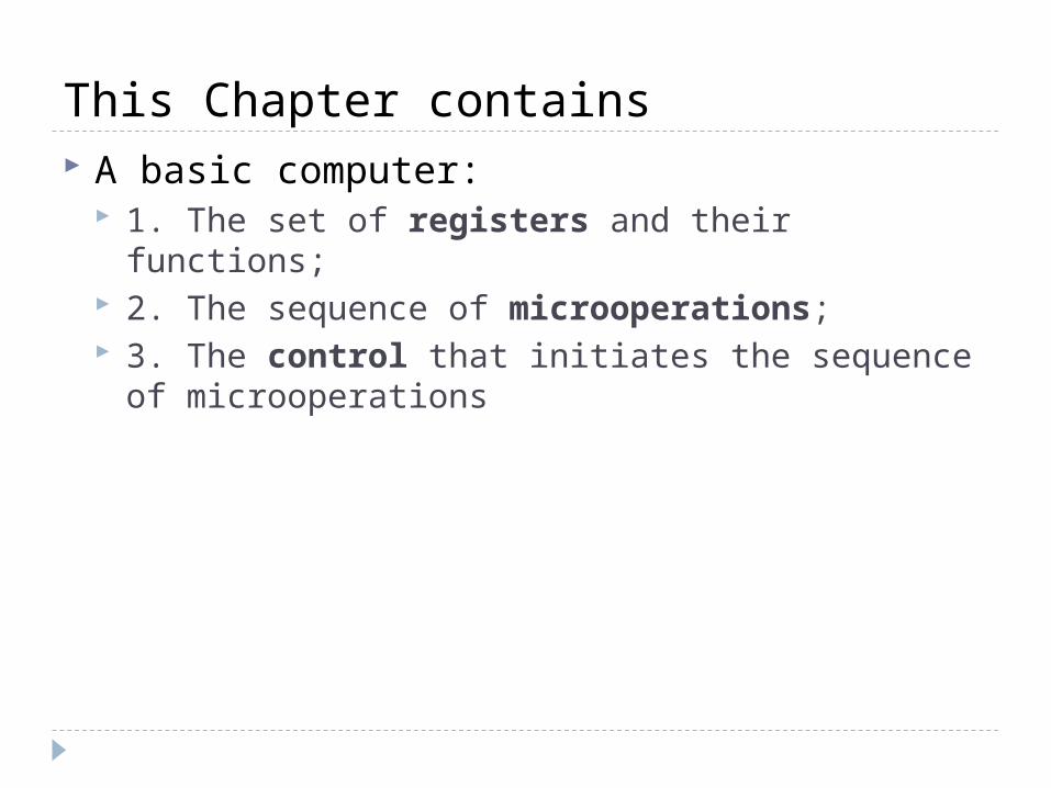
This Chapter contains A basic computer:
1. The set of registers and their functions; 2. The sequence of microoperations; 3. The control that initiates the sequence of
microoperations
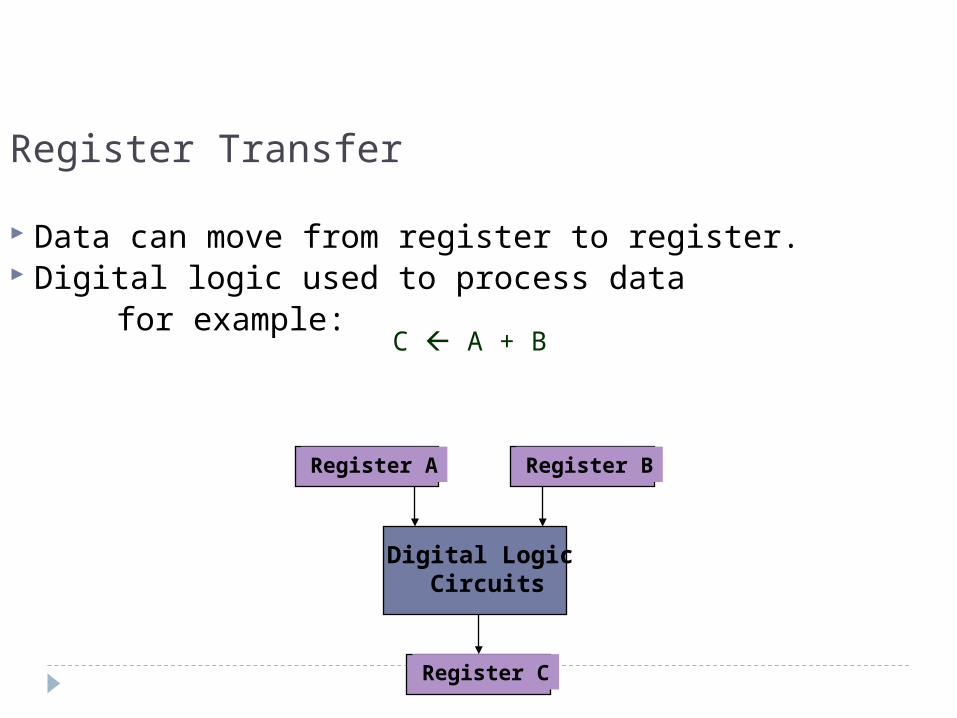
Register Transfer
Data can move from register to register. Digital logic used to process data for example:
Register A Register B
Register C
Digital Logic Circuits
C A + B
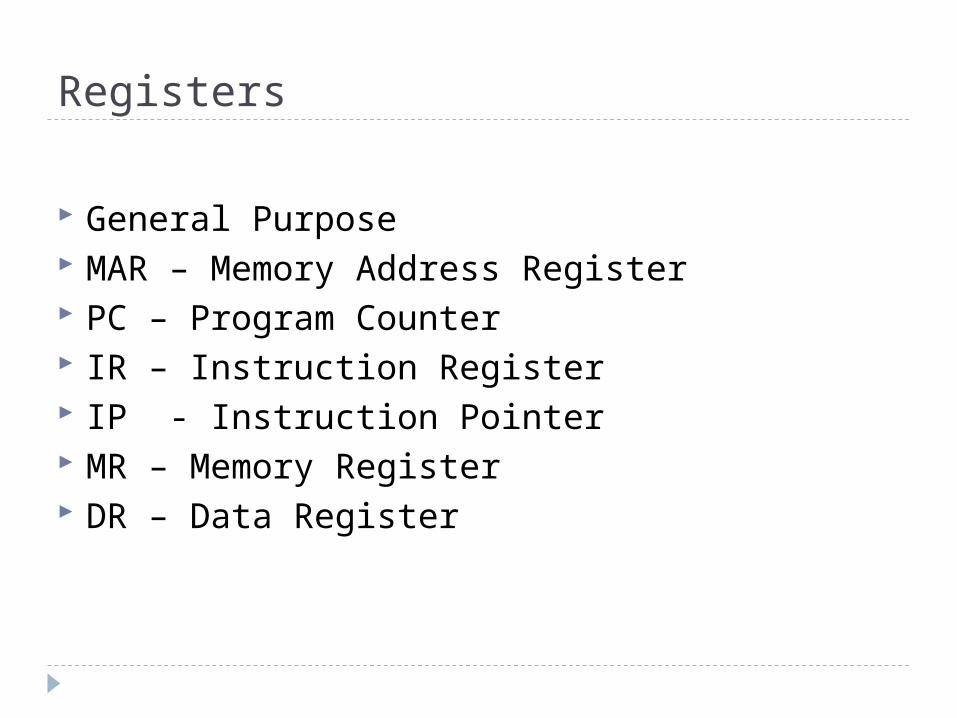
Registers
General Purpose MAR – Memory Address Register PC – Program Counter IR – Instruction Register IP - Instruction Pointer MR – Memory Register DR – Data Register
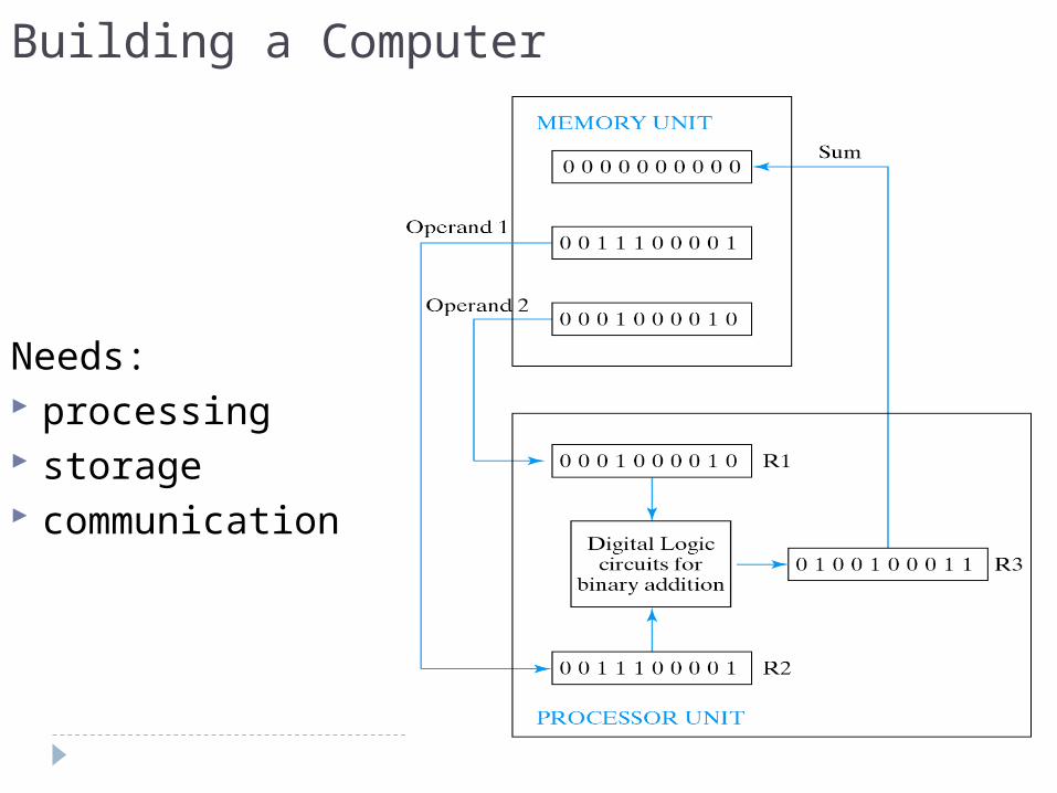
Building a Computer
Needs: processing storage communication
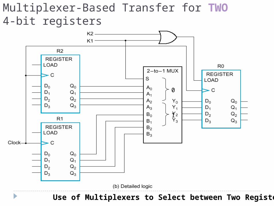
Multiplexer-Based Transfer for TWO 4-bit registers
Use of Multiplexers to Select between Two Registers
0
1

Bus Transfer For register R0 to R3 in a 4 bit system
1 03 2
4*1MUX 3
1 03 2
1 03 2
4*1MUX 0
1 03 2
1 03 2
4*1MUX 1
1 03 2
1 03 2
4*1MUX 2
1 03 2
S1 S0 Register selected 0 0 A 0 1 B 1 0 C 1 1 D
S1S0
4-linecommonbus
Register D Register C Register B Register A
Used for highest bit from each register
Used for lowest bit
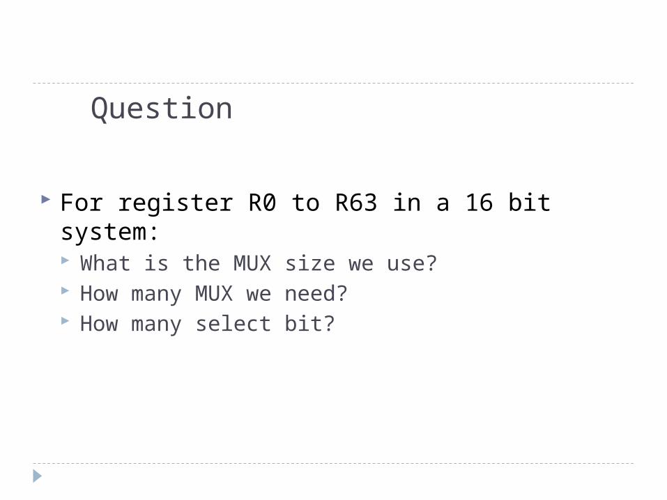
Question
For register R0 to R63 in a 16 bit system: What is the MUX size we use? How many MUX we need? How many select bit?

Three-State Bus Buffers
A bus system can be constructed with three-state gates instead of multiplexers
Tri-State : 0, 1, High-impedance(Open circuit)
Buffer A device designed to be inserted between other devices
to match impedance, to prevent mixed interactions, and to supply additional drive or relay capability

Tri-state buffer gate Tri-state buffer gate : Fig. 4-4
When control input =1 : The output is enabled(output Y = input A)
When control input =0 : The output is disabled(output Y = high-impedance)
Normal input A
Control input C
If C=1, Output Y = A
If C=0, Output = High-impedance
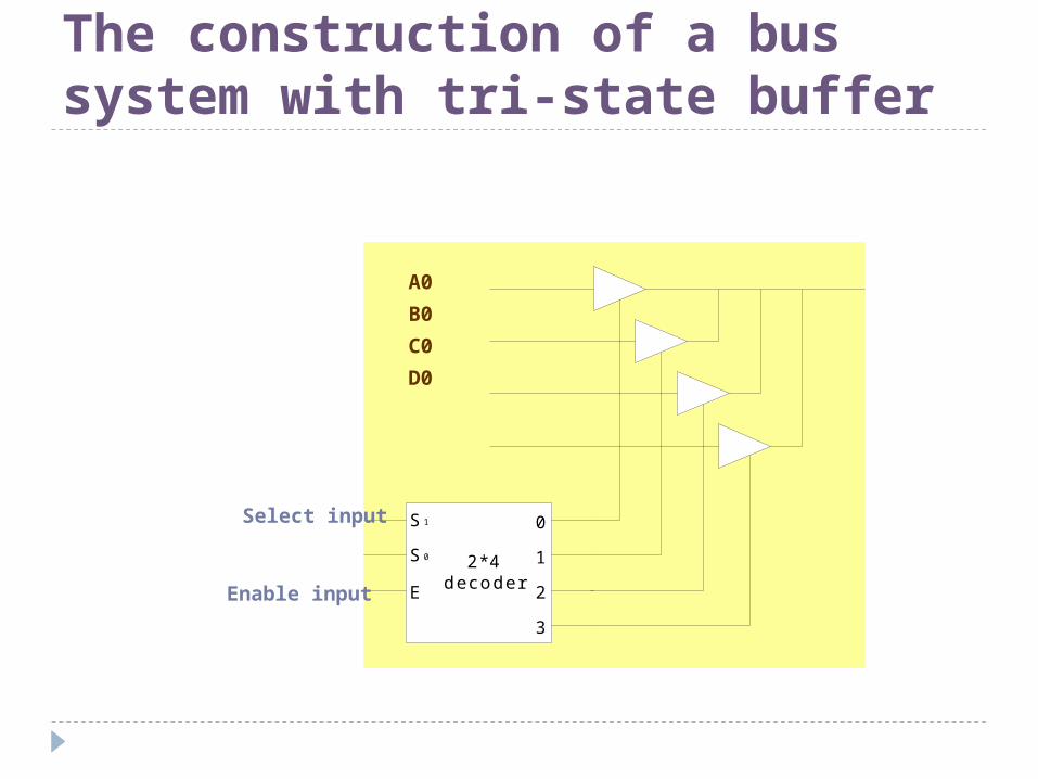
The construction of a bus system with tri-state buffer
0
3
1
2
S 0
S 1
E
2*4decoder
A0
B0
C0
D0
Select input
Enable input
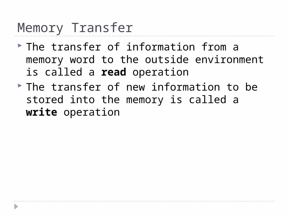
Memory Transfer The transfer of information from a memory
word to the outside environment is called a read operation
The transfer of new information to be stored into the memory is called a write operation
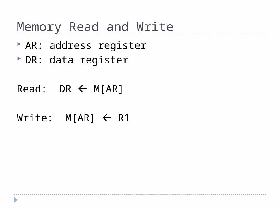
Memory Read and Write AR: address register DR: data register
Read: DR M[AR]
Write: M[AR] R1
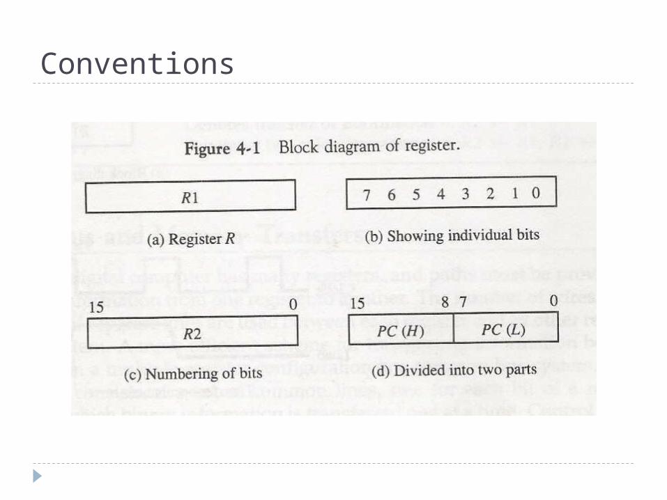
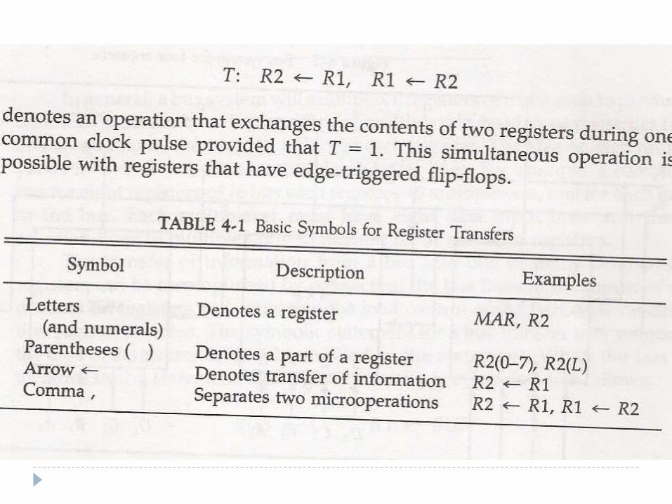
Conventions
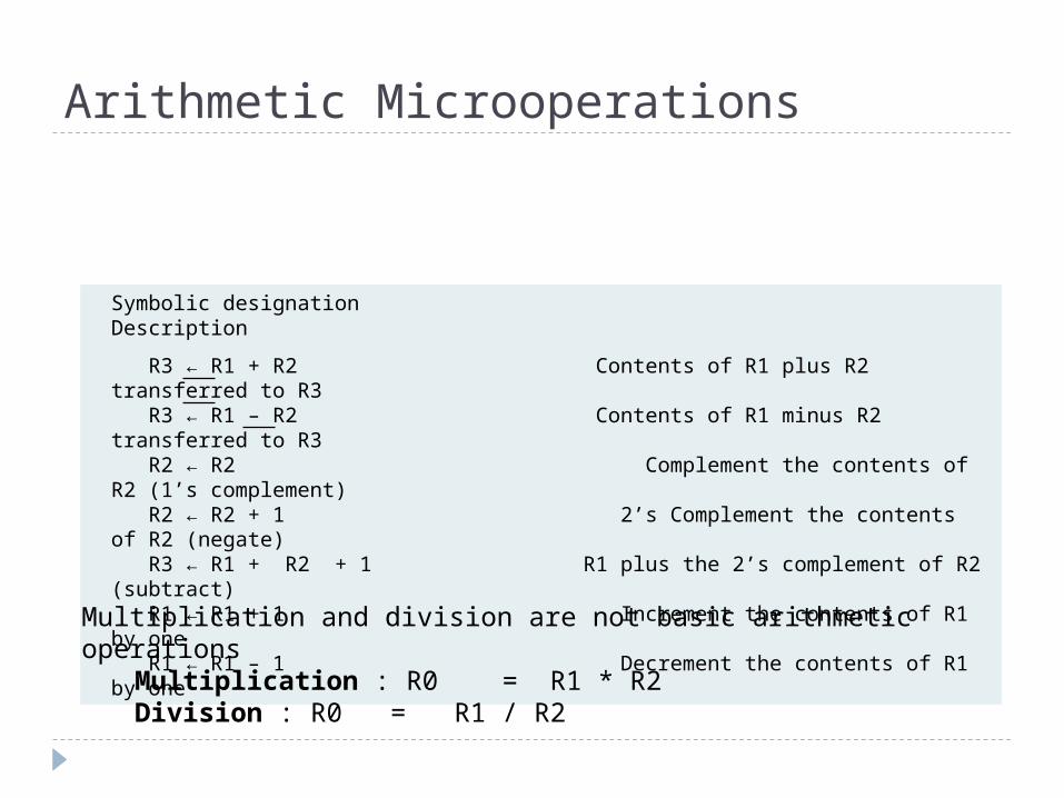
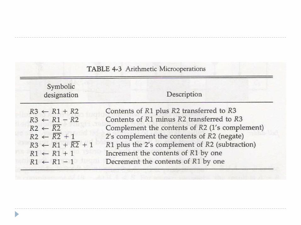
Arithmetic Microoperations
Symbolic designation Description
R3 ← R1 + R2 Contents of R1 plus R2 transferred to R3 R3 ← R1 – R2 Contents of R1 minus R2 transferred to R3 R2 ← R2 Complement the contents of R2 (1’s complement) R2 ← R2 + 1 2’s Complement the contents of R2 (negate) R3 ← R1 + R2 + 1 R1 plus the 2’s complement of R2 (subtract) R1 ← R1 + 1 Increment the contents of R1 by one R1 ← R1 – 1 Decrement the contents of R1 by one
Multiplication and division are not basic arithmetic operationsMultiplication : R0 = R1 * R2Division : R0 = R1 / R2
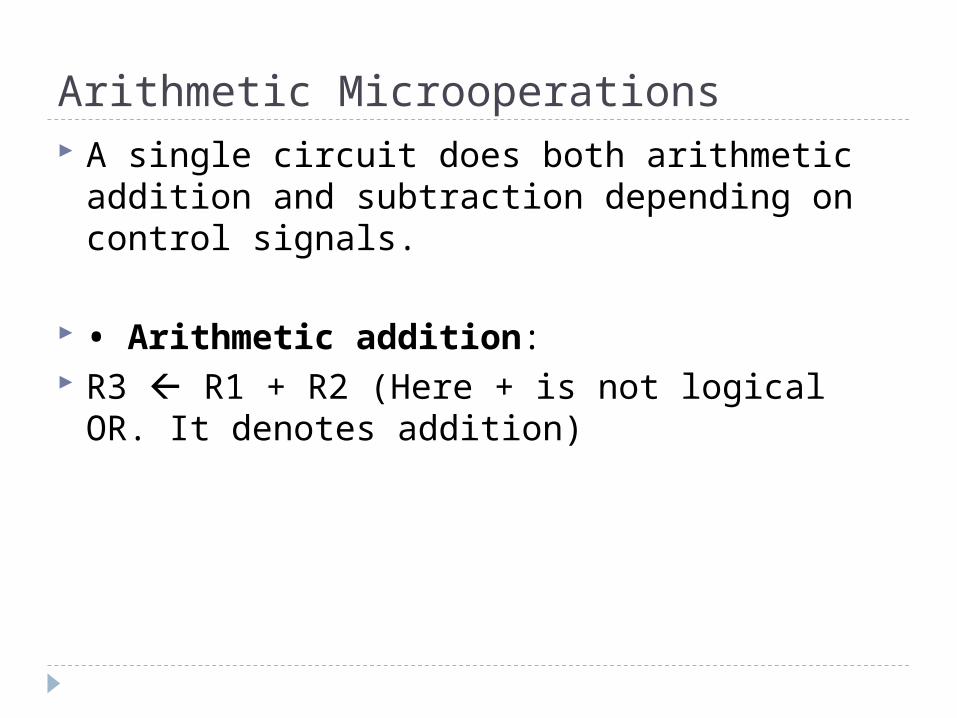
Arithmetic Microoperations A single circuit does both arithmetic addition
and subtraction depending on control signals.
• Arithmetic addition: R3 R1 + R2 (Here + is not logical OR. It
denotes addition)
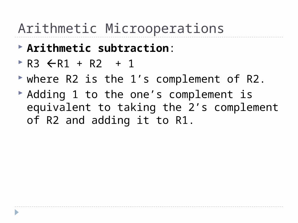
Arithmetic Microoperations Arithmetic subtraction: R3 R1 + R2 + 1 where R2 is the 1’s complement of R2. Adding 1 to the one’s complement is
equivalent to taking the 2’s complement of R2 and adding it to R1.

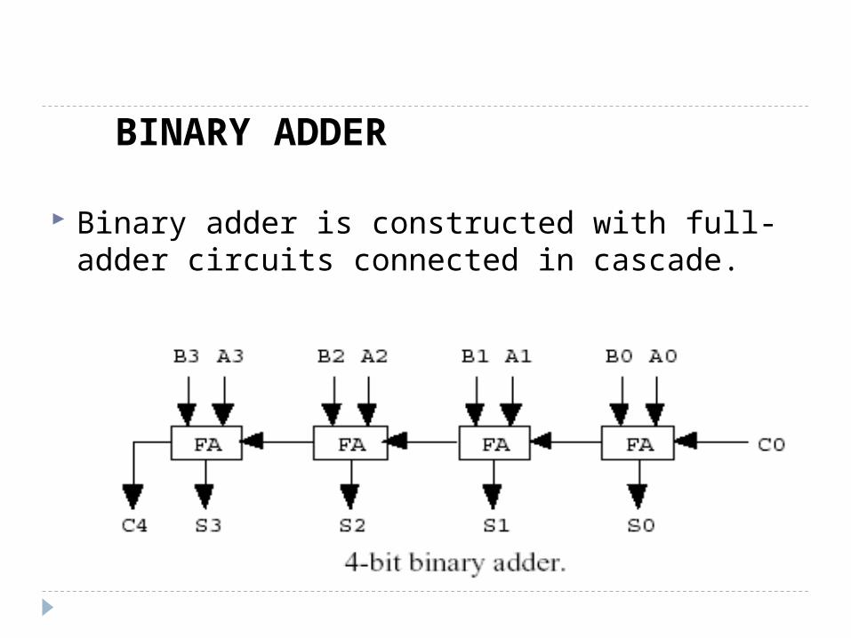
BINARY ADDER
Binary adder is constructed with full-adder circuits connected in cascade.

BINARY ADDER-SUBTRACTOR(104-105)• The addition and subtraction operations cane be
combined into one common circuit by including an exclusive-OR gate with each full-adder.
XORM b0 0 0 0 1 11 0 11 1 0
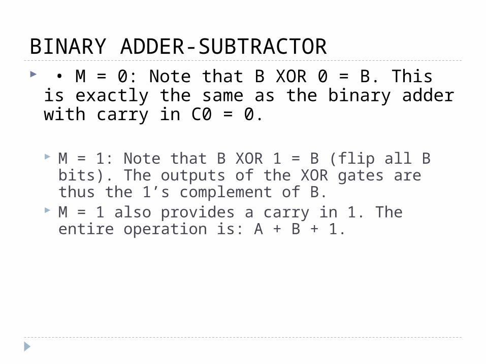
BINARY ADDER-SUBTRACTOR • M = 0: Note that B XOR 0 = B. This is
exactly the same as the binary adder with carry in C0 = 0.
M = 1: Note that B XOR 1 = B (flip all B bits). The outputs of the XOR gates are thus the 1’s complement of B.
M = 1 also provides a carry in 1. The entire operation is: A + B + 1.
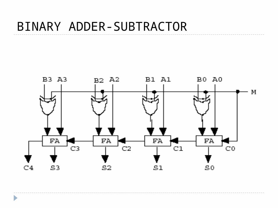
BINARY ADDER-SUBTRACTOR
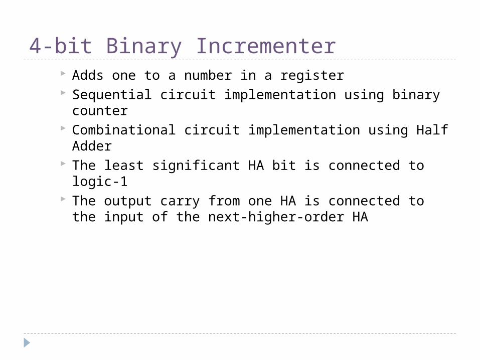
4-bit Binary Incrementer Adds one to a number in a register Sequential circuit implementation using binary counter Combinational circuit implementation using Half Adder The least significant HA bit is connected to logic-1 The output carry from one HA is connected to the input
of the next-higher-order HA
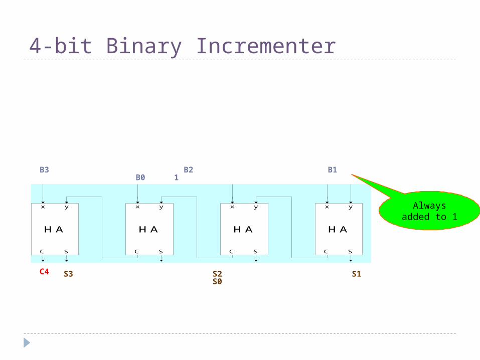
4-bit Binary Incrementer
x
S
y
C
HA
x
S
y
C
HA
x
S
y
C
HA
x
S
y
C
HA
B3 B2 B1 B0 1
Always added to 1
C4 S3 S2 S1 S0
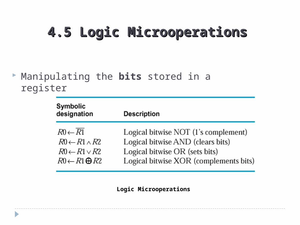
Manipulating the bits stored in a register
4.5 Logic Microoperations4.5 Logic Microoperations
Logic Microoperations
Arithmetic Circuit (106-107)

Clear Logic operation can…
1)clear a group of bit values (Anding the bits to be cleared with zeros)
10101101 10101011 R1 (data)00000000 11111111 R2 (mask)
00000000 10101011 R1

Set2) set a group of bit values (Oring the bits to be
set to ones with ones)10101101 10101011 R1 (data)11111111 00000000 R2 (mask)
11111111 10101011 R1
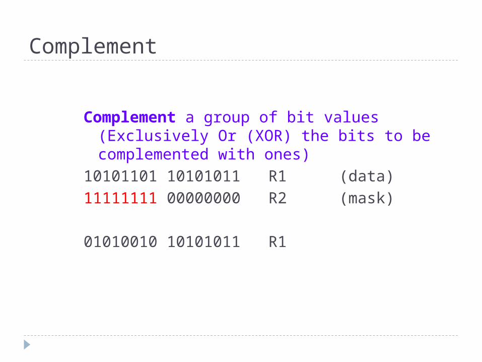
Complement
Complement a group of bit values (Exclusively Or (XOR) the bits to be complemented with ones)
10101101 10101011 R1 (data)11111111 00000000 R2 (mask)
01010010 10101011 R1

• A variety of logic gates are inserted for each bit of registers. Different bitwise logical operations are selected by select signals.
LOGIC CIRCUIT
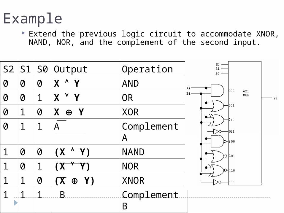
Example Extend the previous logic circuit to accommodate XNOR,
NAND, NOR, and the complement of the second input.
S2
S1
S0
Output Operation
0 0 0 X Y AND
0 0 1 X Y OR
0 1 0 X Y XOR
0 1 1 A Complement A
1 0 0 (X Y) NAND
1 0 1 (X Y) NOR
1 1 0 (X Y) XNOR
1 1 1 B Complement B
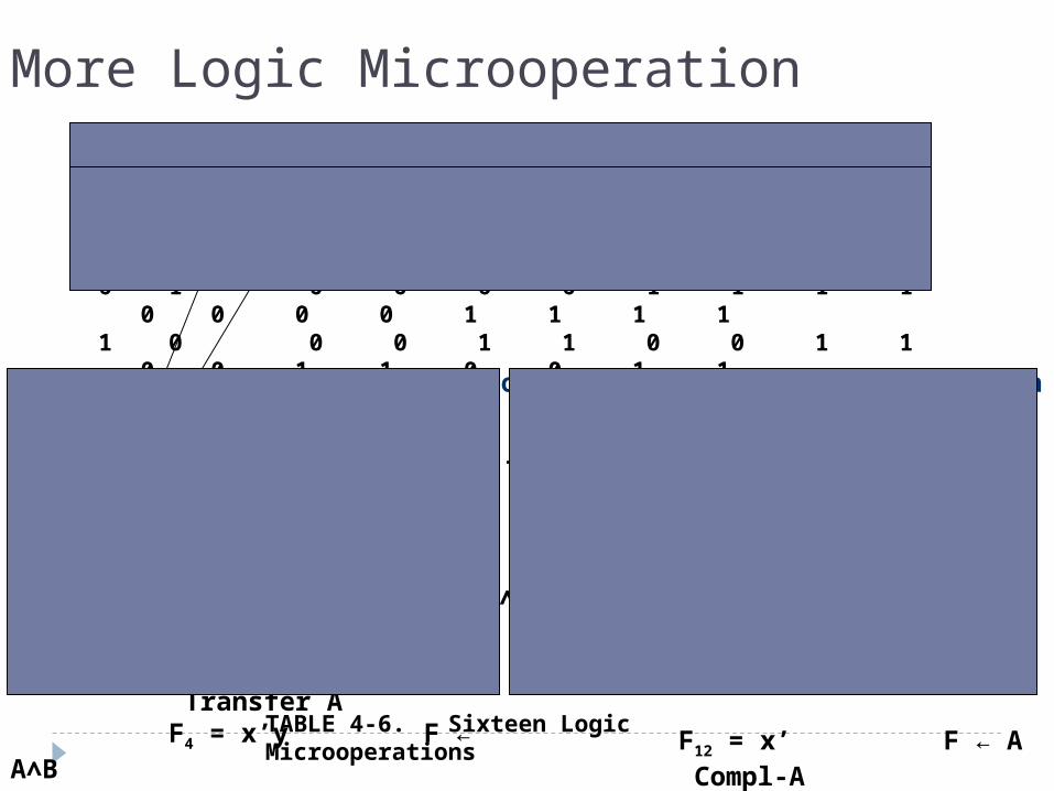
More Logic Microoperation
TABLE 4-6. Sixteen Logic Microoperations
X Y F0 F1 F2 F3 F4 F5 F6 F7 F8 F9 F10 F11 F12 F13 F14 F15
0 0 0 0 0 0 0 0 0 0 1 1 1 1 1 1 1 1 0 1 0 0 0 0 1 1 1 1 0 0 0 0 1 1 1 11 0 0 0 1 1 0 0 1 1 0 0 1 1 0 0 1 11 1 0 1 0 1 0 1 0 1 0 1 0 1 0 1 0 1
TABLE 4-5. Truth Table for 16 Functions of Two Variables
Boolean function Microoperation Name
F0 = 0 F ← 0 Clear F1 = xy F ← A∧B AND F2 = xy’ F ← A∧B F3 = x F ← A Transfer A F4 = x’y F ← A∧B F5 = y F ← B Transfer B
F6 = x y F ← A B Ex-OR F7 = x+y F ← A∨B OR
Boolean function Microoperation Name
F8 = (x+y)’ F ← A∨B NOR
F9 = (x y)’ F ← A B Ex-NOR
F10 = y’ F ← B Compl-B
F11 = x+y’ F ← A∨B F12 = x’ F ← A Compl-A F13 = x’+y F ← A∨B F14 = (xy)’ F ← A∧B NAND F15 = 1 F ← all 1’s set to all 1’s
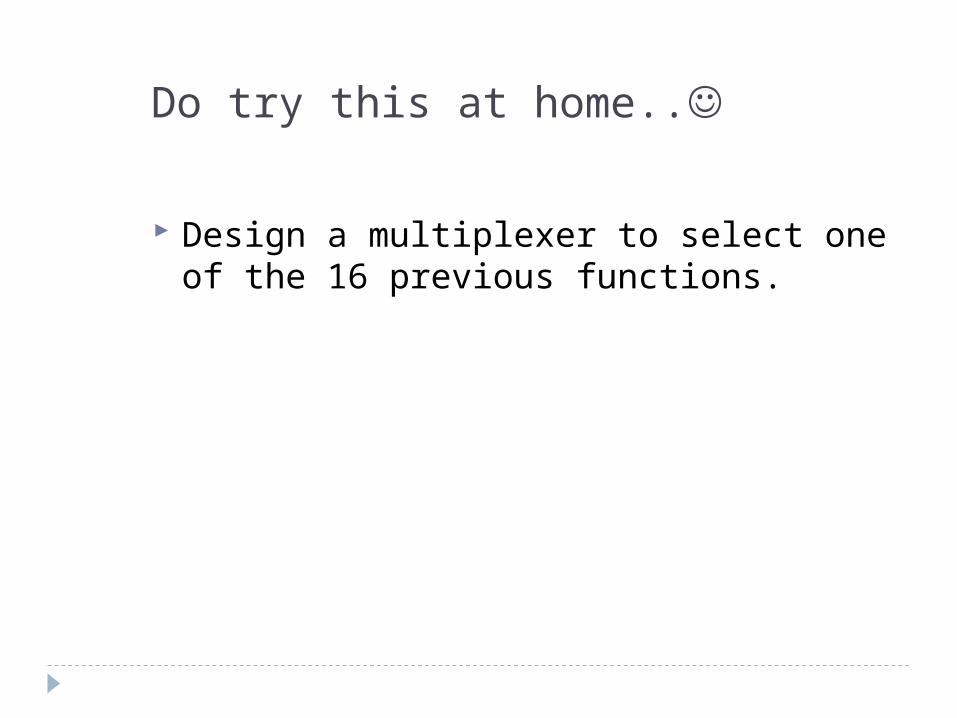
Do try this at home..
Design a multiplexer to select one of the 16 previous functions.
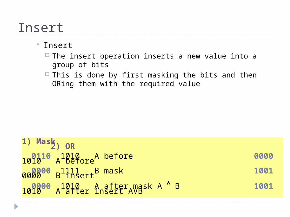
Insert Insert
The insert operation inserts a new value into a group of bits This is done by first masking the bits and then ORing them
with the required value
1) Mask 2) OR 0110 1010 A before 0000 1010 A before 0000 1111 B mask 1001 0000 B insert 0000 1010 A after mask A B 1001 1010 A after insert AVB
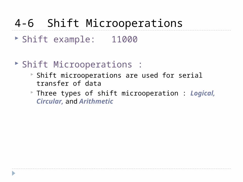
4-6 Shift Microoperations Shift example: 11000
Shift Microoperations : Shift microoperations are used for serial transfer of data Three types of shift microoperation : Logical, Circular,
and Arithmetic
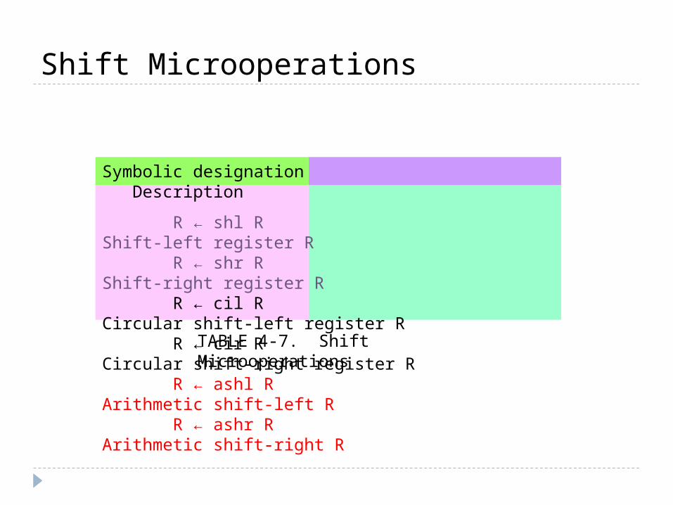
Shift Microoperations
Symbolic designation Description
R ← shl R Shift-left register R R ← shr R Shift-right register R R ← cil R Circular shift-left register R R ← cir R Circular shift-right register R R ← ashl R Arithmetic shift-left R R ← ashr R Arithmetic shift-right R
TABLE 4-7. Shift Microoperations
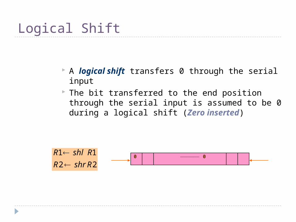
Logical Shift
A logical shift transfers 0 through the serial input The bit transferred to the end position through the
serial input is assumed to be 0 during a logical shift (Zero inserted)
22
11
RshrR
RshlR
0 0

Logical Shift Example
1. Logical shift: Transfers 0 through the serial input.R1 shl R1 Logical shift-leftR2 shr R2 Logical shift-right(Example) Logical shift-left10100011 01000110

Circular Shift The circular shift circulates the bits of the register
around the two ends without loss of information

Circular Shift Example
22
11
RcirR
RcilR
Circular shift-left
Circular shift-right
(Example) Circular shift-left
10100011 is shifted to 01000111
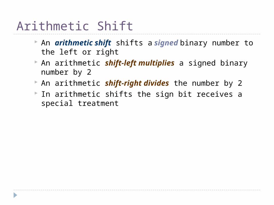
Arithmetic Shift An arithmetic shift shifts a signed binary number to
the left or right An arithmetic shift-left multiplies a signed binary
number by 2 An arithmetic shift-right divides the number by 2 In arithmetic shifts the sign bit receives a special
treatment
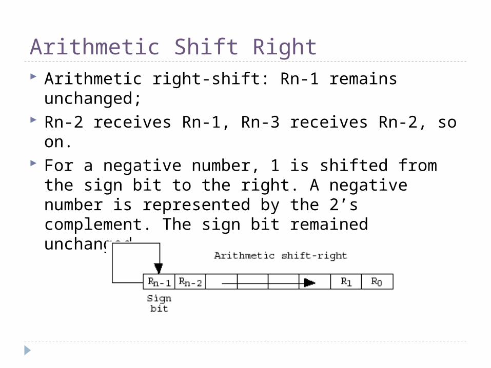
Arithmetic Shift Right Arithmetic right-shift: Rn-1 remains unchanged; Rn-2 receives Rn-1, Rn-3 receives Rn-2, so on. For a negative number, 1 is shifted from the sign
bit to the right. A negative number is represented by the 2’s complement. The sign bit remained unchanged.

Arithmetic Shift Right Arithmetic Shift Right :
Example 1
0100 (4) 0010 (2)
Example 2
1010 (-6) 1101 (-3)

Arithmetic Shift Left
22 RashlR
LSB
Carry outSign bit
Rn-1 Rn-2
Vs=1 : OverflowVs=0 : use sign bit
LSB
0 insert
The operation is same with Logic shift-left
The only difference is you need to check overflow problem
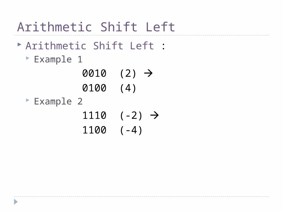
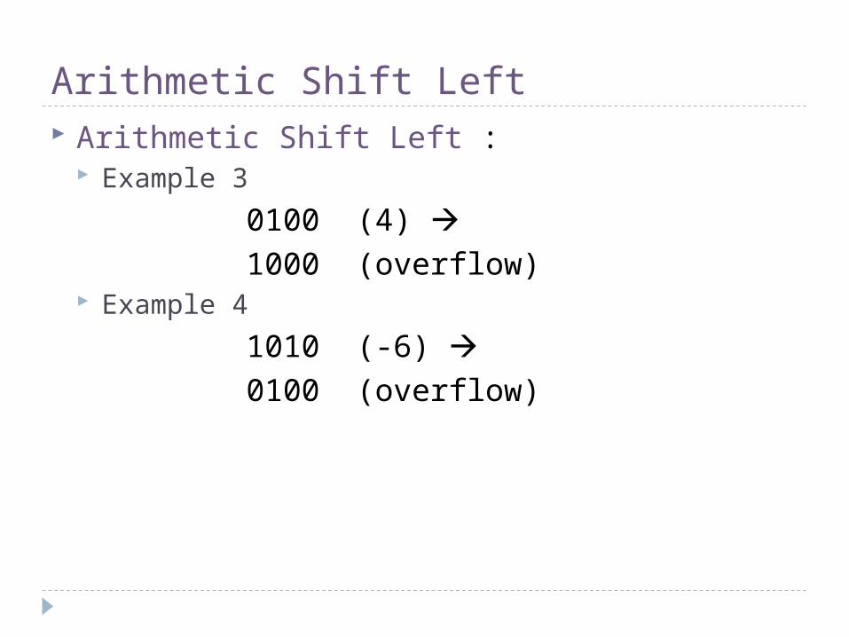
Arithmetic Shift Left Arithmetic Shift Left :
Example 1
0010 (2) 0100 (4)
Example 2
1110 (-2) 1100 (-4)
Arithmetic Shift Left Arithmetic Shift Left :
Example 3
0100 (4) 1000 (overflow)
Example 4
1010 (-6) 0100 (overflow)