CHAPTER 4 MARIE: An Introduction to a Simple Computer€¦ · CHAPTER 4 MARIE: An Introduction to a...
24
CMPS375 Class Notes (Chap04) Page 1 / 24 by Kuo-pao Yang CHAPTER 4 MARIE: An Introduction to a Simple Computer 4.1 Introduction 177 4.2 CPU Basics and Organization 177 4.2.1 The Registers 178 4.2.2 The ALU 179 4.2.3 The Control Unit 179 4.3 The Bus 179 4.4 Clocks 183 4.5 The Input/Output Subsystem 185 4.6 Memory Organization and Addressing 186 4.7 Interrupts 189 4.8 MARIE 190 4.8.1 The Architecture 190 4.8.2 Registers and Buses 190 4.8.3 The Instruction Set Architecture 193 4.8.4 Register Transfer Notation 195 4.9 Instruction Processing 198 4.9.1 The Fetch-Decode-Execute Cycle 198 4.9.2 Interrupts and the Instruction Cycle 199 4.9.3 MARIE’s I/O 203 4.10 A Simple Program 203 4.11 A Discussion on Assemblers 206 4.11.1 What Do Assemblers Do? 206 4.11.2 Why Use Assembly Language? 208 4.12 Extending Our Instruction Set 209 4.13 A Discussion on Decoding: Hardwired vs. Microprogrammed Control 214 4.13.1 Machine Control 214 4.13.2 Hardwired Control 216 4.13.3 Microprogrammed Control 217 4.14 Real-World Examples of Computer Architectures 223 4.14.1 Intel Architectures 224 4.14.2 MIPS Architectures 230 Chapter Summary 233
Transcript of CHAPTER 4 MARIE: An Introduction to a Simple Computer€¦ · CHAPTER 4 MARIE: An Introduction to a...
CMPS375 Class Notes (Chap04) Page 1 / 24 by Kuo-pao Yang
CHAPTER 4
MARIE: An Introduction to a Simple Computer 4.1 Introduction 177 4.2 CPU Basics and Organization 177
4.2.1 The Registers 178 4.2.2 The ALU 179 4.2.3 The Control Unit 179
4.3 The Bus 179 4.4 Clocks 183 4.5 The Input/Output Subsystem 185 4.6 Memory Organization and Addressing 186 4.7 Interrupts 189 4.8 MARIE 190
4.8.1 The Architecture 190 4.8.2 Registers and Buses 190 4.8.3 The Instruction Set Architecture 193 4.8.4 Register Transfer Notation 195
4.9 Instruction Processing 198 4.9.1 The Fetch-Decode-Execute Cycle 198 4.9.2 Interrupts and the Instruction Cycle 199 4.9.3 MARIE’s I/O 203
4.10 A Simple Program 203 4.11 A Discussion on Assemblers 206
4.11.1 What Do Assemblers Do? 206 4.11.2 Why Use Assembly Language? 208
4.12 Extending Our Instruction Set 209 4.13 A Discussion on Decoding: Hardwired vs. Microprogrammed Control 214
4.13.1 Machine Control 214 4.13.2 Hardwired Control 216 4.13.3 Microprogrammed Control 217
4.14 Real-World Examples of Computer Architectures 223 4.14.1 Intel Architectures 224 4.14.2 MIPS Architectures 230
Chapter Summary 233

CMPS375 Class Notes (Chap04) Page 2 / 24 by Kuo-pao Yang
4.1 Introduction 177 • In this chapter, we first look at a very simple computer called MARIE: A Machine
Architecture that is Really Intuitive and Easy. • We then provide brief overviews of Intel and MIPS machines, two popular
architectures reflecting the CISC (Complex Instruction Set Computer) and RISC (Reduced Instruction Set Computer) design philosophies.
• The objective of this chapter is to give you an understanding of how a computer functions.
4.2 CPU Basics and Organization 177 • The Central processing unit (CPU) is responsible for fetching program instructions,
decoding each instruction that is fetched, and executing the indicated sequence of operations on the correct data.
• All computers have a CPU that can be divide into two pieces: datapath and the control unit.
• The datapath consists of an arithmetic-logic unit (ALU) and storage units (registers) that are interconnected by a data bus that is also connected to main memory. Check page 29 Figure 1.4.
• Various CPU components perform sequenced operations according to signals provided by its control unit.
4.2.1 The Registers 178 • Registers hold data that can be readily accessed by the CPU. • They can be implemented using D flip-flops. A 32-bit register requires 32 D flip-flops. 4.2.2 The ALU 179 • The arithmetic-logic unit (ALU) carries out logical operations (such as comparisons)
and arithmetic operations (such as add or multiply) directed by the control unit. 4.2.3 The Control Unit 179 • The control unit determines which actions to carry out according to the values in a
program counter register and a status register.
CMPS375 Class Notes (Chap04) Page 3 / 24 by Kuo-pao Yang
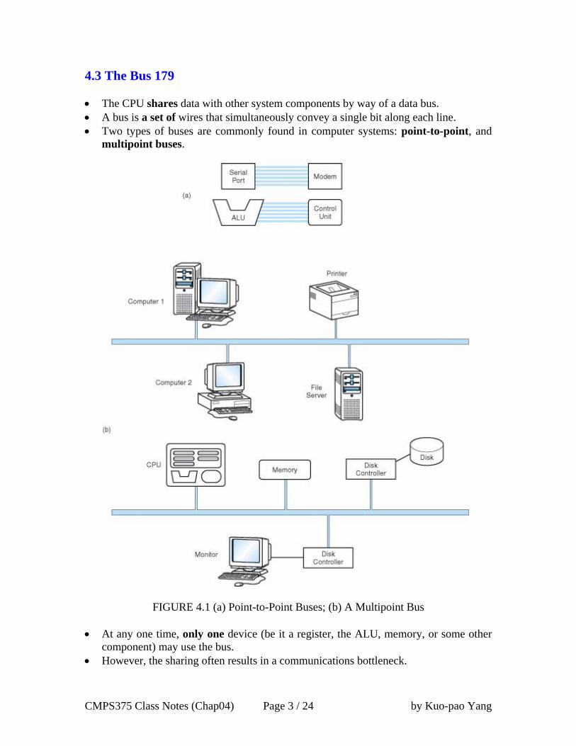
4.3 The Bus 179 • The CPU shares data with other system components by way of a data bus. • A bus is a set of wires that simultaneously convey a single bit along each line. • Two types of buses are commonly found in computer systems: point-to-point, and
multipoint buses.
FIGURE 4.1 (a) Point-to-Point Buses; (b) A Multipoint Bus
• At any one time, only one device (be it a register, the ALU, memory, or some other
component) may use the bus. • However, the sharing often results in a communications bottleneck.

CMPS375 Class Notes (Chap04) Page 4 / 24 by Kuo-pao Yang
• Master device is one that initiates actions and a slave responds to requests by a master.
• Buses consist of data lines, control lines, and address lines. • While the data lines convey bits from one device to another, control lines determine
the direction of data flow, and when each device can access the bus. • Address lines determine the location of the source or destination of the data.
FIGURE 4.2 The Components of a Typical Bus • In a master-slave configuration, where more than one device can be the bus master,
concurrent bus master requests must be arbitrated. • Four categories of bus arbitration are:
o Daisy chain: Permissions are passed from the highest priority device to the lowest.
o Centralized parallel: Each device is directly connected to an arbitration circuit, and a centralized arbiter selects who gets the bus.
o Distributed using self-detection: Devices decide which gets the bus among themselves.
o Distributed using collision-detection: Any device can try to use the bus. If its data collides with the data of another device, the device tries again (Ethernet uses this type arbitration).

CMPS375 Class Notes (Chap04) Page 5 / 24 by Kuo-pao Yang
4.4 Clocks 183 • Every computer contains at least one clock that synchronizes the activities of its
components. • A fixed number of clock cycles are required to carry out each data movement or
computational operation. • The clock frequency, measured in megahertz or gigahertz, determines the speed with
which all operations are carried out. • Clock cycle time is the reciprocal of clock frequency.
o An 800 MHz clock has a cycle time of 1.25 ns. • The minimum clock cycle time must be at least as great as the maximum
propagation delay of the circuit. • The CPU time required to run a program is given by the general performance
equation:
• We see that we can improve CPU throughput when we reduce the number of
instructions in a program, reduce the number of cycles per instruction, or reduce the number of nanoseconds per clock cycle.
• In general, multiplication requires more time than addition, floating point operations require more cycles than integer ones, and accessing memory takes longer than accessing registers.
• Bus clocks are usually slower than CPU clocks, causing bottleneck problems. 4.5 The Input/Output Subsystem 185 • I/O devices allow us to communicate with the computer system. A computer
communicates with the outside world through its input/output (I/O) subsystem. • I/O is the transfer of data between primary memory and various I/O peripherals. • I/O devices are not connected directly to the CPU. I/O devices connect to the CPU
through various interfaces. • The CPU communicates to these external devices via input/output registers. • This exchange of data is performed in two ways:
o In memory-mapped I/O, the registers in the interface appear in the computer’s memory and there is no real difference accessing memory and accessing an I/O device. It uses up memory space in the system.
o With instruction-based I/O, the CPU has specialized instructions that input and output. Although this does not use memory space, it requires specific I/O instructions.
• Interrupts play a very important part in I/O, because they are an efficient way to notify CPU that input or output is available for use.

CMPS375 Class Notes (Chap04) Page 6 / 24 by Kuo-pao Yang
4.6 Memory Organization and Addressing 186 • You can envision memory as a matrix of bits. • Each row, implemented by a register, has a length typically equivalent to the word
size of machine. • Each register (more commonly referred to as a memory location) has a unique
address; memory addresses usually start at zero and progress upward.
FIGURE 4.4 (a) N 8-Bit Memory Locations; (b) M 16-Bit Memory Locations
• Normally, memory is byte-addressable, which means that each individual byte has a unique address.
• For example, a computer might handle 32-bit word, but still employ a byte-addressable architecture. In this situation, when a word uses multiple bytes, the byte with the lowest address determines the address of the entire word.
• It is also possible that a computer might be word-addressable, which means each word has its own address, but most current machines are byte-addressable.
• If architecture is byte-addressable, and the instruction set architecture word is larger than 1 byte, the issue of alignment must be addressed.
• Memory is built from random access memory (RAM) chips. Memory is often referred to using the notation L X W (length X Length). For example,
o 4M X 16 means the memory is 4M long (4M = 22 X 220 = 222 words) and it is 16 bits wide (each word is 16 bits).
o To address this memory (assuming word addressing), we need to be able to uniquely identify 222 different items.
o The memory locations for this memory are numbered 0 through 222 -1. o The memory bus of this system requires at least 22 address lines.
• In general, if a computer 2n addressable units of memory, it will require N bits to uniquely address each byte.

CMPS375 Class Notes (Chap04) Page 7 / 24 by Kuo-pao Yang
• Physical memory usually consists of more than one RAM chip.
FIGURE 4.5 Memory as a Collection of RAM Chips (32K X 8)
• Access is more efficient when memory is organized into banks of chips with the addresses interleaved across the chips:
o Accordingly, in high-order interleaving, the high order address bits specify the memory bank.
FIGURE 4.6 High-Order Memory Interleaving (4bytes X 8chips)
o With low-order interleaving, the low order bits of the address specify which memory bank contains the address of interest.
FIGURE 4.7 Low-Order Memory Interleaving (4bytes X 8chips)

CMPS375 Class Notes (Chap04) Page 8 / 24 by Kuo-pao Yang
4.7 Interrupts 189 • Interrupts are events that alter (or interrupt) the normal flow of execution in the
system. An interrupt can be triggered for a variety of reasons, including: o I/O requests o Arithmetic errors (e.g., division by zero) o Arithmetic underflow or overflow o Hardware malfunction (e.g., memory parity error) o User-defined break points (such as when debugging a program) o Page faults (this is covered in detail in Chapter 6) o Invalid instructions (usually resulting from pointer issues) o Miscellaneous o Each interrupt is associated with a procedure that directs the actions of the
CPU when an interrupt occurs.
CMPS375 Class Notes (Chap04) Page 9 / 24 by Kuo-pao Yang
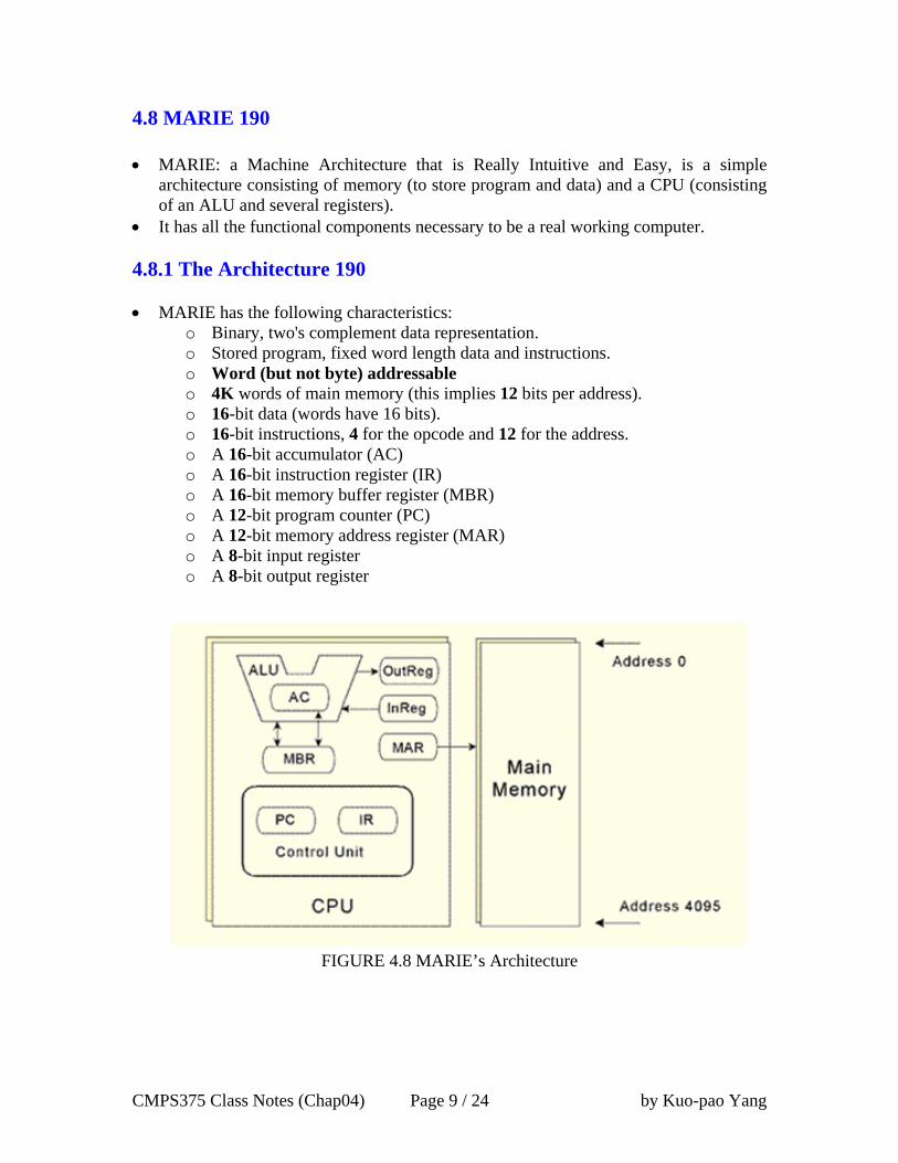
4.8 MARIE 190 • MARIE: a Machine Architecture that is Really Intuitive and Easy, is a simple
architecture consisting of memory (to store program and data) and a CPU (consisting of an ALU and several registers).
• It has all the functional components necessary to be a real working computer. 4.8.1 The Architecture 190 • MARIE has the following characteristics:
o Binary, two's complement data representation. o Stored program, fixed word length data and instructions. o Word (but not byte) addressable o 4K words of main memory (this implies 12 bits per address). o 16-bit data (words have 16 bits). o 16-bit instructions, 4 for the opcode and 12 for the address. o A 16-bit accumulator (AC) o A 16-bit instruction register (IR) o A 16-bit memory buffer register (MBR) o A 12-bit program counter (PC) o A 12-bit memory address register (MAR) o A 8-bit input register o A 8-bit output register
FIGURE 4.8 MARIE’s Architecture
CMPS375 Class Notes (Chap04) Page 10 / 24 by Kuo-pao Yang
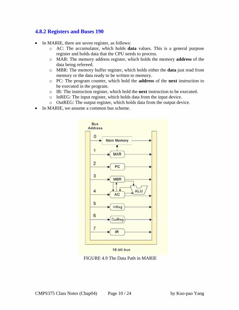
4.8.2 Registers and Buses 190 • In MARIE, there are seven register, as follows:
o AC: The accumulator, which holds data values. This is a general purpose register and holds data that the CPU needs to process.
o MAR: The memory address register, which holds the memory address of the data being refereed.
o MBR: The memory buffer register, which holds either the data just read from memory or the data ready to be written to memory.
o PC: The program counter, which hold the address of the next instruction to be executed in the program.
o IR: The instruction register, which hold the next instruction to be executed. o InREG: The input register, which holds data from the input device. o OutREG: The output register, which holds data from the output device.
• In MARIE, we assume a common bus scheme.
FIGURE 4.9 The Data Path in MARIE
CMPS375 Class Notes (Chap04) Page 11 / 24 by Kuo-pao Yang
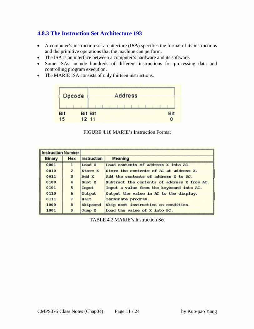
4.8.3 The Instruction Set Architecture 193 • A computer’s instruction set architecture (ISA) specifies the format of its instructions
and the primitive operations that the machine can perform. • The ISA is an interface between a computer’s hardware and its software. • Some ISAs include hundreds of different instructions for processing data and
controlling program execution. • The MARIE ISA consists of only thirteen instructions.
FIGURE 4.10 MARIE’s Instruction Format
TABLE 4.2 MARIE’s Instruction Set

CMPS375 Class Notes (Chap04) Page 12 / 24 by Kuo-pao Yang
4.8.4 Register Transfer Notation 195 • Each of our instructions actually consists of a sequence of smaller instructions called
microoperations. • The symbolic notation used to describe the behavior of microoperations is called
register transfer notation (RTN) or register transfer language (RTL). • In the MARIE RTL, we use the notation M[X] to indicate the actual data value stored
in memory location X, and ← to indicate the transfer of bytes to a register or memory location.
• For example: o Load X The RTL for the LOAD instruction is:
MAR ← X MBR ← M[MAR] AC ← MBR
o Add X The RTL for the ADD instruction is:
MAR ← X MBR ← M[MAR] AC ← AC + MBR
o SKIPCOND skips the next instruction according to the value of the AC.
If IR[11 - 10] = 00 then If AC < 0 then PC ← PC + 1 else If IR[11 - 10] = 01 then If AC = 0 then PC ← PC + 1 else If IR[11 - 10] = 11 then If AC > 0 then PC ← PC + 1

CMPS375 Class Notes (Chap04) Page 13 / 24 by Kuo-pao Yang
4.9 Instruction Processing 198 • All computers follow a basic machine cycle: the fetch, decode, and execute cycle. 4.9.1 The Fetch-Decode-Execute Cycle 198 • The fetch-decode-execute cycle represents the steps that a computer follows to run a
program.
FIGURE 4.11 The Fetch-Decode-Execute Cycle
CMPS375 Class Notes (Chap04) Page 14 / 24 by Kuo-pao Yang
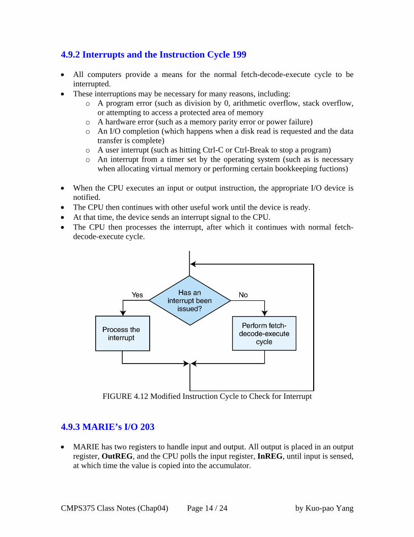
4.9.2 Interrupts and the Instruction Cycle 199 • All computers provide a means for the normal fetch-decode-execute cycle to be
interrupted. • These interruptions may be necessary for many reasons, including:
o A program error (such as division by 0, arithmetic overflow, stack overflow, or attempting to access a protected area of memory
o A hardware error (such as a memory parity error or power failure) o An I/O completion (which happens when a disk read is requested and the data
transfer is complete) o A user interrupt (such as hitting Ctrl-C or Ctrl-Break to stop a program) o An interrupt from a timer set by the operating system (such as is necessary
when allocating virtual memory or performing certain bookkeeping fuctions) • When the CPU executes an input or output instruction, the appropriate I/O device is
notified. • The CPU then continues with other useful work until the device is ready. • At that time, the device sends an interrupt signal to the CPU. • The CPU then processes the interrupt, after which it continues with normal fetch-
decode-execute cycle.
FIGURE 4.12 Modified Instruction Cycle to Check for Interrupt 4.9.3 MARIE’s I/O 203 • MARIE has two registers to handle input and output. All output is placed in an output
register, OutREG, and the CPU polls the input register, InREG, until input is sensed, at which time the value is copied into the accumulator.
CMPS375 Class Notes (Chap04) Page 15 / 24 by Kuo-pao Yang
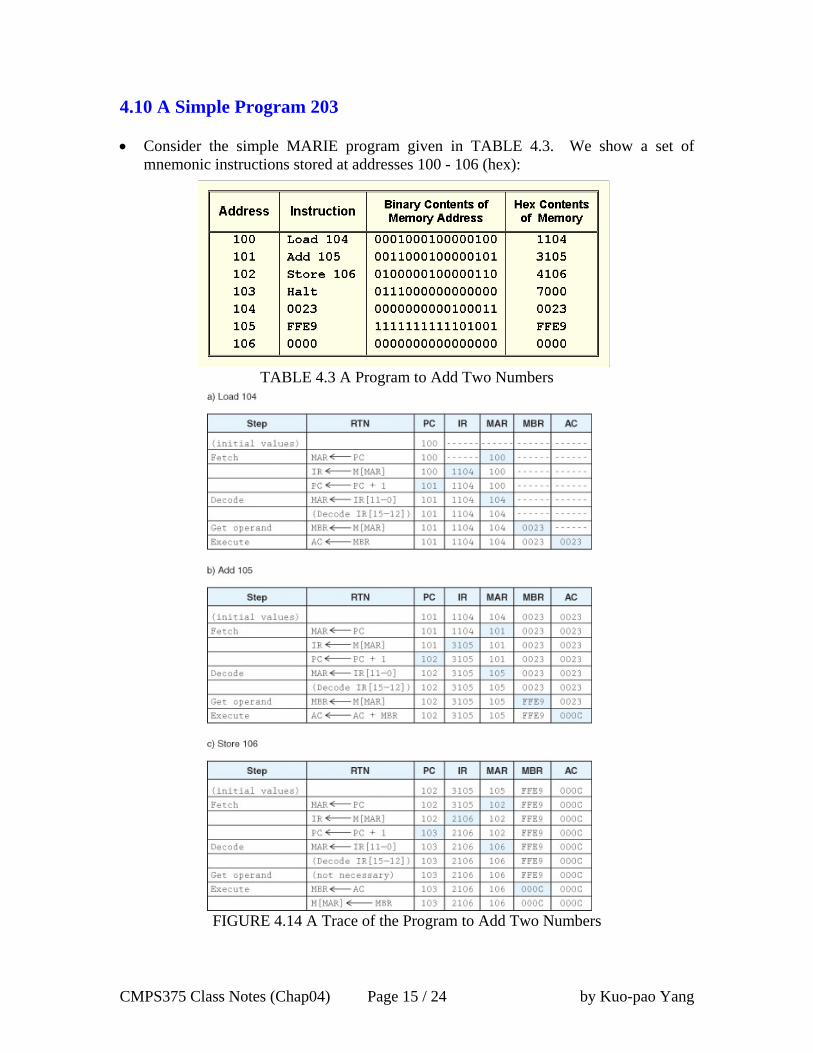
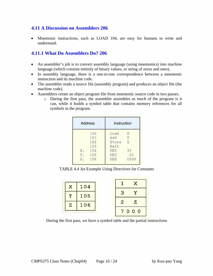
4.10 A Simple Program 203 • Consider the simple MARIE program given in TABLE 4.3. We show a set of
mnemonic instructions stored at addresses 100 - 106 (hex):
TABLE 4.3 A Program to Add Two Numbers
FIGURE 4.14 A Trace of the Program to Add Two Numbers
CMPS375 Class Notes (Chap04) Page 16 / 24 by Kuo-pao Yang
4.11 A Discussion on Assemblers 206 • Mnemonic instructions, such as LOAD 104, are easy for humans to write and
understand. 4.11.1 What Do Assemblers Do? 206 • An assembler’s job is to convert assembly language (using mnemonics) into machine
language (which consists entirely of binary values, or string of zeros and ones). • In assembly language, there is a one-to-one correspondence between a mnemonic
instruction and its machine code. • The assembler reads a source file (assembly program) and produces an object file (the
machine code). • Assemblers create an object program file from mnemonic source code in two passes.
o During the first pass, the assembler assembles as much of the program is it can, while it builds a symbol table that contains memory references for all symbols in the program.
TABLE 4.4 An Example Using Directives for Constants
During the first pass, we have a symbol table and the partial instructions

CMPS375 Class Notes (Chap04) Page 17 / 24 by Kuo-pao Yang
o During the second pass, the instructions are completed using the values from the symbol table.
4.11.2 Why Use Assembly Language? 208 • Most programmers agree that 10% of the code in a program uses approximately 90%
of the CPU time. • In time-critical applications, we often need to optimize this 10% of code.
Programmers can make the program more efficient in terms of time (and space). • If the overall size of the program or response time is critical, assembly language often
becomes the language of choice. • Embedded Systems must be reactive and often are found in time-constrained
environments. These systems are designed to perform either a single instruction or a very specific set of instructions.
• Chance are you use some type of embedded system every day: o Consumer electronics (such as cameras, camcorders, cellular phones, PDAs,
and interactive games) o Consumer products (such as washers, microwave ovens, and washing
machines) o Automobiles (particularly engine control and antilock brakes) o Medical instruments (such as CAT scanners and heart monitors) o Industry (for process controllers and avionics)
CMPS375 Class Notes (Chap04) Page 18 / 24 by Kuo-pao Yang
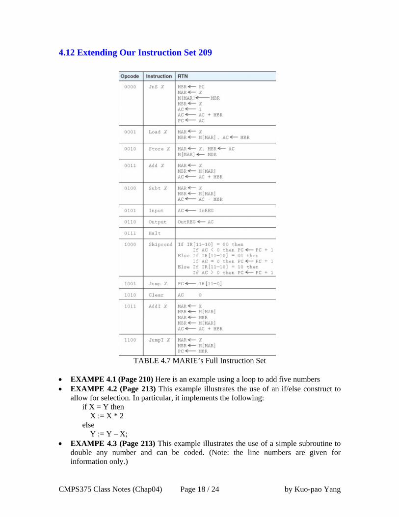
4.12 Extending Our Instruction Set 209
TABLE 4.7 MARIE’s Full Instruction Set • EXAMPE 4.1 (Page 210) Here is an example using a loop to add five numbers • EXAMPE 4.2 (Page 213) This example illustrates the use of an if/else construct to
allow for selection. In particular, it implements the following: if X = Y then X := X * 2 else Y := Y – X;
• EXAMPE 4.3 (Page 213) This example illustrates the use of a simple subroutine to double any number and can be coded. (Note: the line numbers are given for information only.)

CMPS375 Class Notes (Chap04) Page 19 / 24 by Kuo-pao Yang
4.13 A Discussion on Decoding: Hardwired vs. Microprogrammed Control 214 • A computer’s control unit keeps things synchronized, making sure that bits flow to
the correct components as the components are needed. • There are two general ways in which a control unit can be implemented: hardwired
control and microprogrammed control. o With microprogrammed control, a small program is placed into read-only
memory in the microcontroller. o Hardwired controllers implement this program using digital logic components.
4.13.1 Machine Control 214 • P0, P1, P2, controls reading from memory or a register, and the other set consisting of
P3, P4, P5, controls writing to memory or a register. • This register (MBR)is enabled for reading when P0 and P1 are high, and it is enabled
for writing when P3 and P4 are high
FIGURE 4.15 Connection of MARIE’s MBR to the Datapath
CMPS375 Class Notes (Chap04) Page 20 / 24 by Kuo-pao Yang
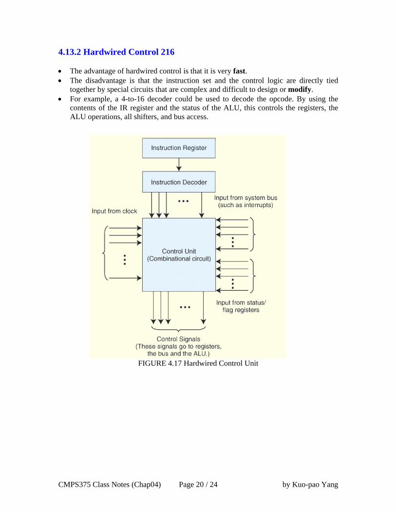
4.13.2 Hardwired Control 216 • The advantage of hardwired control is that it is very fast. • The disadvantage is that the instruction set and the control logic are directly tied
together by special circuits that are complex and difficult to design or modify. • For example, a 4-to-16 decoder could be used to decode the opcode. By using the
contents of the IR register and the status of the ALU, this controls the registers, the ALU operations, all shifters, and bus access.
FIGURE 4.17 Hardwired Control Unit

CMPS375 Class Notes (Chap04) Page 21 / 24 by Kuo-pao Yang
• Careful inspection of MARIE’s RTL reveals that the ALU has only three operations: add, subtract, and clear.
o We will also define a fourth “do nothing” state. • The entire set of MARIE’s control signals consists of:
o Register controls: P0 through P5 (P0P1P2 for read and P3P4P5 for write) o ALU controls: A0 through A1 (do nothing, add, subtract, and clear) o Timing: T0 through T7 and counter reset Cr
• In FIGURE 4.9, Main Memory (address 0 or 111), MAR (address 1 or 001), PC (address 2 or 010), MBR (address 3 or 011), AC (address 4 or 100), InREG (address 5 or 101), OutREG (address or 110), and IR (address 7 or 111).
• Here is the complete signal sequence for MARIE’s Add instruction:
P0P1P2P3T0: MAR <- X // X is in the rightmost 12 bits of the IR; OpCode 0011 (Add) // T0
// P0P1P2: Read from IR (address 7 or 111) // P3: Write to MAR (address 1 or 001)
P3P4T1: MBR <- M[MAR] // T1 // Read from Mem (address 0 or 000)
// P3P4: Write to MBR (address 3 or 011) A0P0P1P5T2: AC <- AC + MBR // T2
// P0P1: Read from MBR (address 3 or 011) // P5: Write to AC (address 4 or 100) // A0: ALU Add (address 1 or 01) CrT3: [Reset counter]
• These signals are ANDed with combinational logic to bring about the desired
machine behavior.
FIGURE 4.18 Combinational Logic for Signal Controls of MARIE’s Add Instruction
CMPS375 Class Notes (Chap04) Page 22 / 24 by Kuo-pao Yang
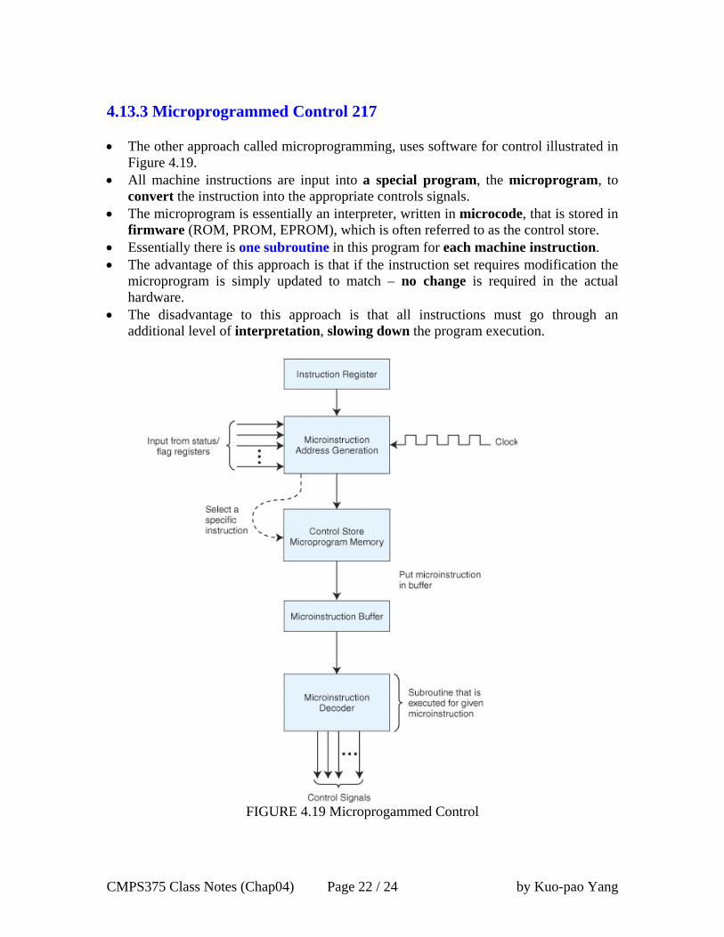
4.13.3 Microprogrammed Control 217 • The other approach called microprogramming, uses software for control illustrated in
Figure 4.19. • All machine instructions are input into a special program, the microprogram, to
convert the instruction into the appropriate controls signals. • The microprogram is essentially an interpreter, written in microcode, that is stored in
firmware (ROM, PROM, EPROM), which is often referred to as the control store. • Essentially there is one subroutine in this program for each machine instruction. • The advantage of this approach is that if the instruction set requires modification the
microprogram is simply updated to match – no change is required in the actual hardware.
• The disadvantage to this approach is that all instructions must go through an additional level of interpretation, slowing down the program execution.
FIGURE 4.19 Microprogammed Control

CMPS375 Class Notes (Chap04) Page 23 / 24 by Kuo-pao Yang
4.14 Real-World Examples of Computer Architectures 223 • Each member of the x86 family of Intel architectures is known as a CISC (Complex
Instruction Set Computer) machine, whereas the Pentium family and the MIPS architectures are examples of RISC (Reduced Instruction Set Computer) machines.
• The main objective of RISC machines is to simplify instructions so they can execute more quickly. Each instruction performs only one operation; they are all the same size.
4.14.1 Intel Architectures 224 • The classic Intel architecture, the 8086, was born in 1979. It is a CISC architecture. • It was adopted by IBM for its famed PC, which was released in 1981. • The 8086 operated on 16-bit data words and supported 20-bit memory addresses. • Later, to lower costs, the 8-bit 8088 was introduced. Like the 8086, it used 20-bit
memory addresses. • In 1985, Intel introduced the 32-bit 80386. • It also had no built-in floating-point unit. • The 80486, introduced in 1989, was an 80386 that had built-in floating-point
processing and cache memory. • The 80386 and 80486 offered downward compatibility with the 8086 and 8088. • Software written for the smaller word systems was directed to use the lower 16 bits of
the 32-bit registers. • Intel’s most advanced 32-bit microprocessor is the Pentium 4. • It can run as fast as 3.06 GHz. This clock rate is over 350 times faster than that of the
8086. • Speed enhancing features include multilevel cache and instruction pipelining. • Intel, along with many others, is marrying many of the ideas of RISC architectures
with microprocessors that are largely CISC. 4.14.2 MIPS Architectures 230 • The MIPS family of CPUs has been one of the most successful in its class. • In 1986 the first MIPS CPU was announced. • It had a 32-bit word size and could address 4GB of memory. • Over the years, MIPS processors have been used in general purpose computers as
well as in games. • The MIPS architecture now offers 32- and 64-bit versions. • MIPS was one of the first RISC microprocessors. • The original MIPS architecture had only 55 different instructions, as compared with
the 8086 which had over 100. • MIPS was designed with performance in mind: It is a load/store architecture, meaning
that only the load and store instructions can access memory.
CMPS375 Class Notes (Chap04) Page 24 / 24 by Kuo-pao Yang
• The large number of registers in the MIPS architecture keeps bus traffic to a minimum.
Chapter Summary 233 • The major components of a computer system are its control unit, registers, memory,
ALU, and data path. • MARIE has 4K 16-bit words of main memory, uses 16-bit instructions, and has seven
registers. • There is only one general purpose register, the AC. • Instructions for MARIE use 4 bits for the opcode and 12 bits for an address. • A built-in clock keeps everything synchronized. • Computers run programs through iterative fetch-decode-execute cycles. • Computers can run programs that are in machine language. • An assembler converts mnemonic code to machine language. • Control units can be microprogrammed or hardwired. • Hardwired control units give better performance, while microprogrammed units are
more adaptable to changes. • The Intel architecture is an example of a CISC architecture; MIPS is an example of a
RISC architecture.