CHAPTER 3 FULLY DIFFERENTIAL DIFFERENCE AMPLIFIER (FDDA...
16
56 CHAPTER 3 FULLY DIFFERENTIAL DIFFERENCE AMPLIFIER (FDDA) BASED ACTIVE FILTER This chapter presents the realization of second order active low pass, high pass and band pass filter using fully differential difference amplifier (FDDA). The fully differential difference amplifier is a balanced output differential difference amplifier. It provides low output distortion and high output voltage swing as compared to the DDA. The filters realized with FDDA possess attractive features that do not exist in both traditional (discrete) and modern fully integrated Op- amp circuits. However the frequency range of operation of FDDA is same as that made of the DDA or Op-Amp. The proposed filters possess orthogonality between the cutoff/central frequency and the quality factor. In view of the orthogonality property, the proposed circuits have wide applications in the instrumentation, control systems and signal processing. All the filter realizations have low sensitivity to parameter variations. The first two sections of this chapter present the implementation of DDA and FDDA. Subsequent sections are devoted to the proposed realization filters and main results. 3.1 DIFFERENTIAL DIFFERENCE AMPLIFIER (DDA) The Differential Difference Amplifier (DDA) is an emerging CMOS analog building block. It has been used in a number of applications such as instrumentation amplifier, continuous time filter, implementation of fully differential switch MOS capacitor circuit, common mode detection circuit, telephone line adaption circuit, biomedical applications, floating resistors, sample and hold circuits and MEMs. [61-89]. Differential Difference Amplifier is an extension of the conventional operational amplifier. An operational amplifier employs only one differential input, whereas two differential inputs in DDA. The schematic diagram of DDA is shown in Figure 3.1. It is a five terminal device with four input terminals named as V pp , V pn , V np , and V nn and the output terminal denoted by V 0 .
Transcript of CHAPTER 3 FULLY DIFFERENTIAL DIFFERENCE AMPLIFIER (FDDA...

56
CHAPTER 3
FULLY DIFFERENTIAL DIFFERENCE AMPLIFIER (FDDA) BASED ACTIVE FILTER
This chapter presents the realization of second order active low pass, high pass and band pass
filter using fully differential difference amplifier (FDDA). The fully differential difference
amplifier is a balanced output differential difference amplifier. It provides low output distortion
and high output voltage swing as compared to the DDA. The filters realized with FDDA possess
attractive features that do not exist in both traditional (discrete) and modern fully integrated Op-
amp circuits. However the frequency range of operation of FDDA is same as that made of the
DDA or Op-Amp.
The proposed filters possess orthogonality between the cutoff/central frequency and the quality
factor. In view of the orthogonality property, the proposed circuits have wide applications in the
instrumentation, control systems and signal processing. All the filter realizations have low
sensitivity to parameter variations. The first two sections of this chapter present the
implementation of DDA and FDDA. Subsequent sections are devoted to the proposed
realization filters and main results.
3.1 DIFFERENTIAL DIFFERENCE AMPLIFIER (DDA)
The Differential Difference Amplifier (DDA) is an emerging CMOS analog building block. It
has been used in a number of applications such as instrumentation amplifier, continuous time
filter, implementation of fully differential switch MOS capacitor circuit, common mode
detection circuit, telephone line adaption circuit, biomedical applications, floating resistors,
sample and hold circuits and MEMs. [61-89].
Differential Difference Amplifier is an extension of the conventional operational amplifier. An
operational amplifier employs only one differential input, whereas two differential inputs in
DDA. The schematic diagram of DDA is shown in Figure 3.1. It is a five terminal device with
four input terminals named as Vpp, Vpn, Vnp, and Vnn and the output terminal denoted by V0.

57
Figure 3.1: The symbol of Differential Difference Amplifier
The block diagram representation of DDA is shown in Figure 3.2. Two voltage-to-current
converters of DDA convert the differential voltage into the current, later these currents are
subtracted and converted into voltage by current to voltage convertor and amplified.
Figure 3.2: The block diagram for DDA
The output voltage v0 of the ideal DDA is characterized by (3.1).
)]()[(00 nnnppnpp VVVVAV −−−= (3.1)
where A0 is open loop gain of DDA. If a negative feedback is introduced at the Vpn or Vnn
terminals, we have
∞→−=− 0 with AVVVV nnnppnpp (3.2)
Unlike operational amplifiers, there exists no virtual ground concept for the analysis of DDA.
Perusal of equation (3.1) suggests that the DDA may be realized by combining three Op-Amps
as in the case of instrumentation amplifier, but it is not true for the following reasons. First,
operational amplifiers are not designed for large differential voltage to be overdriven. Second,
the open loop gain of first two differential amplifiers should match. The DDA is having all the

58
advantages of Op-Amp such as very high open loop gain, high input impedance and low output
impedance. Other than these favorable points, it requires less passive components in realization
of the circuits. Further it may be used in variety of applications such as realization of filters,
mathematical operations, oscillators etc.
J. Huijsing first introduced the DDA by using CMOS technology [61]. Many basic circuits such
as comparator with floating inputs, level shifter, instrumentation amplifier and resistor less unity
gain inverting amplifier using DDA have been realized by Sackinger and Guggebuhl [62]. The
DDA attracted the researchers due to its inherent high input impedances and requirement of less
passive components for realizations of various circuits. Ismail et al. realized DDA based adder,
substractor, multiplier, integrator, filters and phase lead-lag compensator [63- 76]. Soliman and
Soliman proposed current feedback differential difference amplifier with constant bandwidth,
independent of the closed loop gain and with higher slew rate [77]. Angulo et al. realized a
clocked sample and hold circuit using DDA [84]. Chan et al. reported an application of chopper
stabilized DDA as an instrumentation amplifier for electroencephalogram (EEG) [85].
The CMOS implementation of DDA with single output is shown in Figure 3.3.
Figure 3.3 CMOS model of differential difference amplifier
The two differential pairs (M1-M2 and M3-M4) convert the two differential voltages into current
that are subtracted, converted into a voltage by the active load (M5 and M6) and amplified by the
second stage. Compensating capacitor (CC) and resistor (RC) are employed to increase the pole

59
frequency and stability of the circuit. A rail to rail low power output stage is incorporated
consisting of transistors M7-M10 and biasing transistors M14-M15. The output stage is class AB
amplifier such that with no signal applied, no current is drawn from the output terminal. The
current of M9 and M10 are set equal to bias current (ISB). When the current is applied by M9,
transistor M10 will be off. Similarly, when the current is sinking through M10, the transistor M9 is
turned off.
3.2 FULLY DIFFERENTIAL DIFFERENCE AMPLIFIER (FDDA)
Most of the high performance analog integrated circuits incorporate fully differential signal
paths. Fully differential architectures have several advantages over the single ended outputs.
They provide a larger output voltage swing and are less susceptible to common-mode noise.
Also, even-order nonlinearities are not present in the differential output of a balanced circuit,
which is symmetric with perfectly matched elements on the either side of an axis of symmetry.
Disadvantage of a fully differential amplifier is that it requires two matched feedback networks
and a common-mode feedback circuit to control the common-mode output voltage. In 2001,
Ismail et al. [81] proposed the fully differential difference amplifier as shown in Figure 3.4 with
these capabilities.
Figure 3.4: Symbol of Fully Differential Difference Amplifier
The terminal relation of fully differential difference amplifier is expressed as
)]()[(0 nnnppnpponop VVVVAVV −−−=− (3.3)
where A0 is open loop gain of DDA. With a negative feedback applied to the differential
voltages of the two input port, equation (3.3) reduces to (3.2) with ∞→0A .
Vop
Von
Vpn
Vpp
Vnp Vpp

60
If the finite loop gain A0 is decreased, the difference between the two differential voltages
would increase. Therefore open loop gain should be made as large as possible. Like operational
amplifier it consists of mainly of two stages: a differential input transconductance stage and
second gain stage. For low power operation and high current driving capabilities, class-AB
output stage is employed instead of conventional class-A amplifier. The CMOS realization of
the fully differential difference amplifier is shown in Figure 3.5.
Figure 3.5: CMOS Realization of a Fully Differential Difference Amplifier
The CMOS realization of FDDA is similar to DDA. Here differential input pair (M1-M2) and
(M3-M4) convert the differential voltage into currents that are subtracted and converted in to
voltage by active load M5 and M6. Common mode feedback circuit consisting of transistor MC1-
MC7, two capacitors (Ccm), and two resistors (Rcm) are employed to establish the common-
mode output voltage. In the absence of common mode feedback circuit, the common mode
voltage output would drift. Feedback circuit controls the common mode voltage such that it is
equal to some specified voltage (usually mid-rail Vcm) even in the presence of large differential

61
signals. In order to achieve low standby power consumption with good output current driving
capability, two similar class AB rail-to-rail output stages are employed in the circuit. The first
class-AB amplifier consists of transistors M7-M10, and the second one is formed with transistors
M16-M19. Transistors M14 and M15 are used to properly bias both stages of differential amplifier.
Each of the proposed second order low pass, high pass and band pass filter circuit exhibits
orthogonality between the cutoff/central frequency and the bandwidth of the filter. The quality
factor is independently tunable from the cutoff frequency. In the following section the proposed
circuit has been described.
3.3 PROPOSED SECOND ORDER FILTER CIRCUITS
Several filter realization have been obtained using op-amp as active elements. The active
element FDDA requires low power supply for its operations and offers low noise, higher input
differential voltage and higher bandwidth as compared to operational amplifier. Since second
order filters are the basic building blocks for designing the higher order filters, the focus has
been made on the realization of second order filters only as discussed earlier. The proposed
realizations of second order low pass, high pass and band pass filters, employing active element
FDDA and passive elements (resistors and capacitors) are presented in the following
subsections.
3.3.1 LOW PASS FILTER A second order low pass filter is realized by employing one FDDA, with eight resistors and
three capacitors as shown in Figure 3.6.

62
Figure 3.6: Low pass filter circuit diagram using FDDA
The transfer function of this circuit is given by equation (3.4)
4231232143
2
4231
1111)(
CCRRCRCRCRkss
CCRRk
sTLP
+⎟⎟⎠
⎞⎜⎜⎝
⎛++
−+
=
(3.4)
where 2
11X
X
RRk +=
The cutoff frequency 0ω and the quality factor Q of the above circuit are:
42310
1CCRR
=ω (3.5)
43
21
23
41
21
43 )1(1CRCRk
CRCR
CRCR
Q−++=
(3.6)
The simplified expressions for the cutoff frequency ω0 and the quality factor Q may be obtained
with the constraint of equal spread of resistors and capacitors i.e.
RRR == 31 and CCC == 42 .
Vip
Vin
Vop
Von
R1
R1
R3
R3
Rx2 Rx1
Rx2 Rx
C4
C2
C2

63
k
QRC−== 31 and 1
0ω (3.7)
The sensitivities to parameter variation are shown in (3.8)-(3.10).
21
0
4231 ,,, −=ωCCRRS (3.8)
51
31 , =QRRS
(3.9)
9.042 , −=Q
CCS
(3.10)
Thus, the sensitivities of the realization are not more than one. The magnitude and phase
responses of the low pass filter, shown in Figure 3.7 match the desired specifications. For the
realization of the low pass filter, shown in Figure 3.6, the capacitors and resistors are taken as C
= 70 nF and R = 1.59 kΩ to provide a cutoff frequency f0 = 1.43 kHz and Q = 2 The low pass
circuit employs an amplifier with finite gain k = 2.5.
Figure 3.7 (a): Low pass filter magnitude response using FDDA

64
Figure 3.7(b): Low pass filter phase response using FDDA
3.3.2 HIGH PASS FILTER High-pass filters are often formed by interchanging resistors and capacitors in the low pass
filters. The circuit of high pass filter employing FDDA and passive components is shown in
Figure 3.8.
Figure 3.8: High pass filter circuit diagram using FDDA
Vip
Vin
Vop
Von
C1
C1
C3
C3
Rx2 Rx1
Rx2Rx
R4
R2
R2

65
The transfer function of the high pass filter employing fully differential difference amplifier
shown in Figure 3.8 is
3142143412
2
2
1111)(
CCRRCRCRCRkss
kssTHP
+⎟⎟⎠
⎞⎜⎜⎝
⎛++
−+
=(3.11)
Thus
31420
1CCRR
=ω (3.12)
12
34
14
32
34
12 )1(1CRCR
kCRCR
CRCR
Q−++=
(3.13)
where,
2
11X
X
RRk +=
The simplified expressions for the cutoff frequency ω0 and the quality factor Q may be obtained
with the constraint of equal spread of resistors and capacitors i.e. R4 = 2*R2 = R and C1 = C3 =
C.
kQRC
−== 31 and 10ω (3.14)
The sensitivities to parameter variation are as follows
21
0
3142 ,,, −=ωCCRRS (3.15)
51
42 , =QRRS (3.16)
9.031, −=Q
CCS
(3.17)

66
The magnitude and phase responses of the high pass filter, shown in Figure 3.9, match the
desired specifications. For the realization of the high pass filter, shown in Figure 3.8, the
capacitors and resistors are taken as C = 70 nF and R = 1.59 kΩ to provide a cutoff frequency f0
= 1.43 kHz and Q = 2. The high pass circuit employs an amplifier with finite gain k = 2.5.
Figure 3.9 (a) : High pass filter circuit magnitude response using FDDA
Figure 3.9(b): High pass filter circuit phase response using FDDA

67
3.3.3 BAND PASS FILTER
The proposed band pass filter, shown in Figure 3.10, has been realized by combining the low
pass and high passes filter circuits. It realizes a band pass filter with wide bandwidth which is
difference of two cutoff frequencies fH and fL respectively of high pass and low pass filters, with
fH > fL.
Figure 3.10: Band pass filter circuit diagram using FDDA
The transfer function of the band pass filter circuit is expressed in equation (3.18)
⎟⎟⎠
⎞⎜⎜⎝
⎛++⎟⎟
⎠
⎞⎜⎜⎝
⎛++
−++
=
2153434545251
2
51
1111111)(
RRCCRCRCRCRk
CRss
CRsk
sTBP
(3.18)
where, 2
11X
X
RRk +=
Thus the cutoff frequency and the quality factor may be obtained as given by equation (3.19)
and (3.20):
Vip
Vin
Vop
Von
R1
R1
C3
C3
Rx2 Rx1
Rx2Rx1
R4
R2
R2
C5
68
5341
2
1
0
1
CCRRRR
+=ω
(3.19)
and
⎟⎟⎠
⎞⎜⎜⎝
⎛++
−+
+=
3454525121
53421 11111CRCRCR
kCRRR
CCRRRQ
(3.20)
The design equations may be obtained by pre selection of elements with equal spread as
follows:
RRRR === 321
CCC == 53
With these constrains the simplified expressions for the central frequency and the quality factor
are given by:
RC2
0 =ω and
32
=Q
The sensitivities to parameter variation of the band pass filter are:
35.00
21 , =ωRRS
5.00
5,3,4−=ω
CCRS
4749.01
−=QRS
9393.02=Q
RS

69
7573.04
−=QRS
2323.03=Q
CS
0606.05=Q
CS
The sensitivity of the filter response with parameter variation is less than unity.
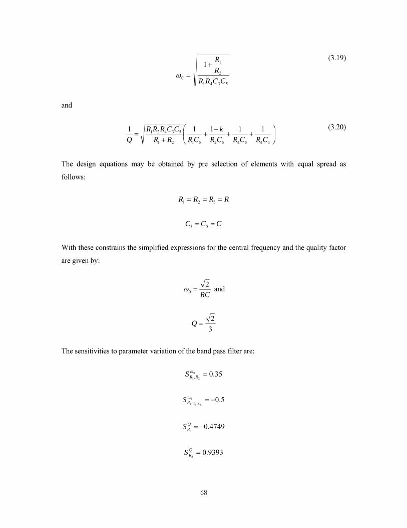
The magnitude and phase response of the band pass filter is shown in Figure 3.11 match the
designed specifications, for the cutoff frequency 2.02 kHz by employing C = 70nF and R = 1.59
kΩ.
Figure 3.11(a): Band pass filter circuit magnitude response using FDDA
70
Figure 3.11(b): Band pass filter circuit phase response using FDDA
3.4 SIMULATION RESULTS
The industry standard circuit simulator PSPICE simulation software has been employed for
simulation of the active element FDDA on 90nm CMOS technology using ±1.5V supply
voltage. The basic circuit proposed by Alzaher and Ismail [81] has been adopted for simulation.
The filter response shows 40dB slope, which corresponds to second order transfer function.
Though the designed filter has orthogonality between quality factor and the central frequency,
the Q of the realized band pass filter is not very high. Because of dependence of the quality
factor on gain of the amplifier, the sensitivity turns out to be poor for high Q realizations. This
band-pass filter realization may therefore be used in the IF amplifier stage.
3.5 CONCLUSION
The FDDA is a circuit element similar to the OTA at the input side and to the op-amp at the
output side. It can therefore be used for designing DDA-based circuits, with special properties
of both OTAs and Op-amps. That is, the circuits designed with FDDA have high input
impedance, low component count, low output impedance and low distortion. Thus, the filters

71
realized with FDDA, though operating in the frequency range of op-amps possess attractive
features that do not exist in both traditional (discrete) and modern fully integrated op-amp
circuits. The proposed filter has low value of Q, so it can be used where flat response is needed.
All realizations have low sensitivity to parameter variation.


![Informationstechnische/r Assistent/in (ITA) - DIPLOMA€¦ · DIPLOMA Hochschule Am Hegeberg 2 37242 Bad Sooden-Allendorf Tel. +49 [0] 5652 587770 Fax +49 [0] 5652 5877729 info@diploma.de](https://static.fdocuments.net/doc/165x107/5f07446b7e708231d41c239e/informationstechnischer-assistentin-ita-diploma-diploma-hochschule-am-hegeberg.jpg)