Chapter 3 Chapter 3 :: Topics - University of Houston...
26
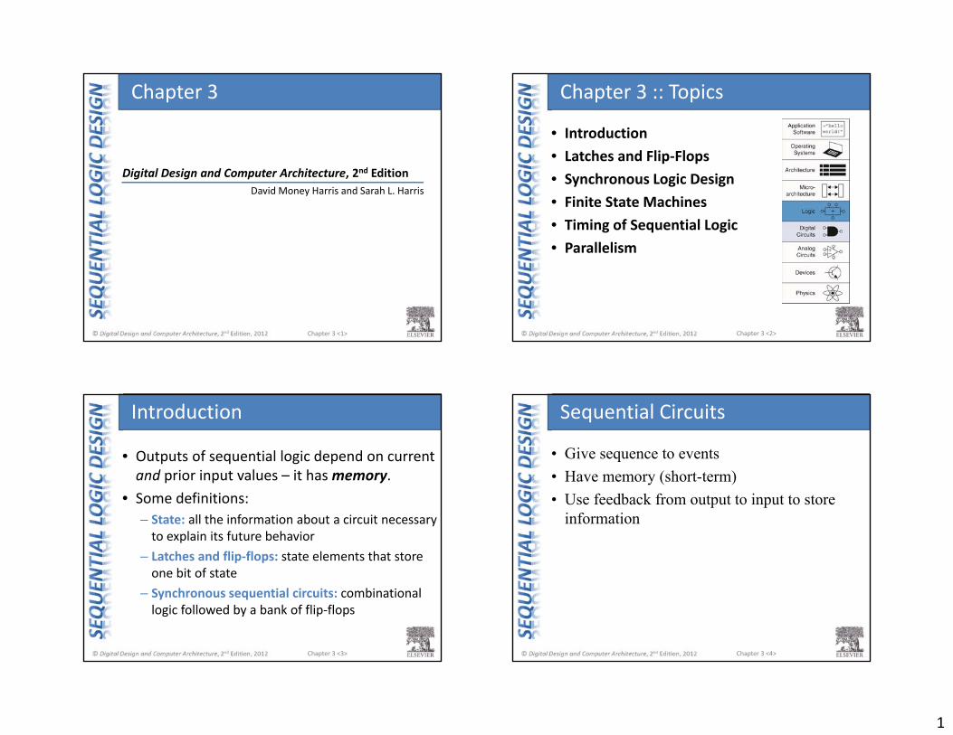
1 Chapter 3 <1> Digital Design and Computer Architecture, 2 nd Edition Chapter 3 David Money Harris and Sarah L. Harris Chapter 3 <2> Chapter 3 :: Topics • Introduction • Latches and Flip‐Flops • Synchronous Logic Design • Finite State Machines • Timing of Sequential Logic • Parallelism Chapter 3 <3> • Outputs of sequential logic depend on current and prior input values – it has memory. • Some definitions: – State: all the information about a circuit necessary to explain its future behavior – Latches and flip‐flops: state elements that store one bit of state – Synchronous sequential circuits: combinational logic followed by a bank of flip‐flops Introduction Chapter 3 <4> • Give sequence to events • Have memory (short-term) • Use feedback from output to input to store information Sequential Circuits
-
Upload
truongkiet -
Category
Documents
-
view
226 -
download
1
Transcript of Chapter 3 Chapter 3 :: Topics - University of Houston...
1
Chapter 3 <1>
Digital Design and Computer Architecture, 2nd Edition
Chapter 3
David Money Harris and Sarah L. Harris
Chapter 3 <2>
Chapter 3 :: Topics
• Introduction• Latches and Flip‐Flops• Synchronous Logic Design• Finite State Machines• Timing of Sequential Logic• Parallelism
Chapter 3 <3>
• Outputs of sequential logic depend on current and prior input values – it has memory.
• Some definitions:– State: all the information about a circuit necessary to explain its future behavior
– Latches and flip‐flops: state elements that store one bit of state
– Synchronous sequential circuits: combinational logic followed by a bank of flip‐flops
Introduction
Chapter 3 <4>
• Give sequence to events• Have memory (short-term)• Use feedback from output to input to store
information
Sequential Circuits
2
Chapter 3 <5>
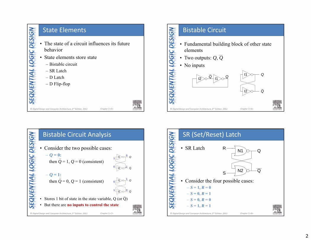
• The state of a circuit influences its future behavior
• State elements store state– Bistable circuit– SR Latch– D Latch– D Flip-flop
State Elements
Chapter 3 <6>
QQ Q
Q
I1
I2
I2 I1
• Fundamental building block of other state elements
• Two outputs: Q, Q• No inputs
Bistable Circuit
Chapter 3 <7>
Q
Q
I1
I2
0
1
1
0
Q
Q
I1
I2
1
0
0
1
• Consider the two possible cases:– Q = 0:
then Q = 1, Q = 0 (consistent)
– Q = 1: then Q = 0, Q = 1 (consistent)
• Stores 1 bit of state in the state variable, Q (or Q)• But there are no inputs to control the state
Bistable Circuit Analysis
Chapter 3 <8>
R
S
Q
Q
N1
N2
• SR Latch
• Consider the four possible cases:– S = 1, R = 0– S = 0, R = 1– S = 0, R = 0– S = 1, R = 1
SR (Set/Reset) Latch
3
Chapter 3 <9>
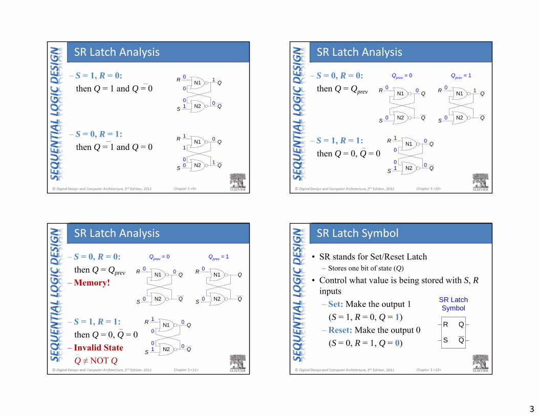
– S = 1, R = 0: then Q = 1 and Q = 0
– S = 0, R = 1: then Q = 1 and Q = 0
SR Latch Analysis
R
S
Q
Q
N1
N2
0
1
1
00
0
R
S
Q
Q
N1
N2
1
0
0
10
1
Chapter 3 <10>
R
S
Q
Q
N1
N2
0
0
R
S
Q
Q
N1
N2
0
0
0
Qprev = 0 Qprev = 1
1
– S = 0, R = 0: then Q = Qprev
– S = 1, R = 1: then Q = 0, Q = 0
SR Latch Analysis
R
S
Q
Q
N1
N2
1
1
0
00
0
Chapter 3 <11>
R
S
Q
Q
N1
N2
0
0
R
S
Q
Q
N1
N2
0
0
0
Qprev = 0 Qprev = 1– S = 0, R = 0: then Q = Qprev
– Memory!
– S = 1, R = 1: then Q = 0, Q = 0
– Invalid StateQ ≠ NOT Q
SR Latch Analysis
R
S
Q
Q
N1
N2
1
1
0
00
0
Chapter 3 <12>
S
R Q
Q
SR LatchSymbol
• SR stands for Set/Reset Latch– Stores one bit of state (Q)
• Control what value is being stored with S, Rinputs– Set: Make the output 1
(S = 1, R = 0, Q = 1)– Reset: Make the output 0
(S = 0, R = 1, Q = 0)
SR Latch Symbol
4
Chapter 3 <13>
D LatchSymbol
CLK
D Q
Q
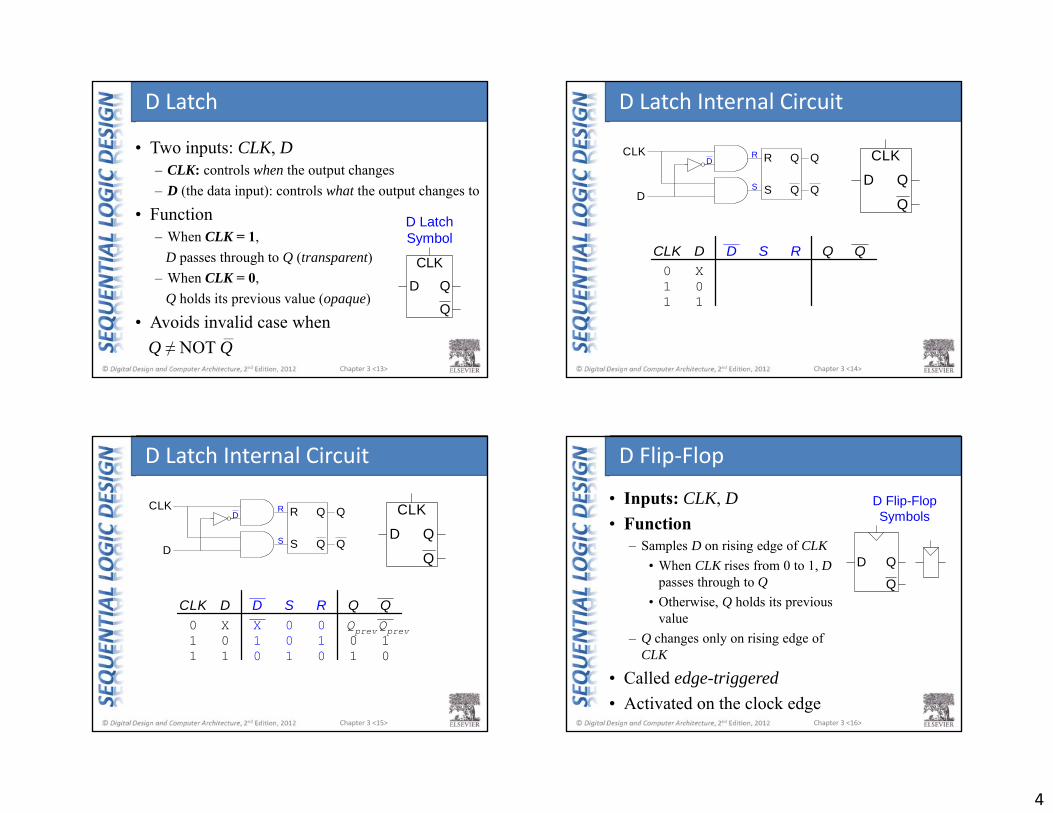
• Two inputs: CLK, D– CLK: controls when the output changes– D (the data input): controls what the output changes to
• Function– When CLK = 1,
D passes through to Q (transparent)– When CLK = 0,
Q holds its previous value (opaque)
• Avoids invalid case when Q ≠ NOT Q
D Latch
Chapter 3 <14>
S
R Q
Q
Q
QD
CLKD
R
S
CLK
D Q
Q
S R Q QCLK D0 X1 01 1
D
D Latch Internal Circuit
Chapter 3 <15>
S
R Q
Q
Q
QD
CLKD
R
S
CLK
D Q
Q
S R Q0 0 Qprev0 1 01 0 1
Q
10
CLK D0 X1 01 1
DX10
Qprev
D Latch Internal Circuit
Chapter 3 <16>
D Flip-FlopSymbols
D Q
Q
• Inputs: CLK, D• Function
– Samples D on rising edge of CLK• When CLK rises from 0 to 1, D
passes through to Q• Otherwise, Q holds its previous
value– Q changes only on rising edge of
CLK
• Called edge-triggered• Activated on the clock edge
D Flip‐Flop
5
Chapter 3 <17>
CLK
D Q
Q
CLK
D Q
Q
Q
Q
D N1
CLK
L1 L2
• Two back-to-back latches (L1 and L2) controlled by complementary clocks
• When CLK = 0– L1 is transparent– L2 is opaque– D passes through to N1
• When CLK = 1– L2 is transparent– L1 is opaque– N1 passes through to Q
• Thus, on the edge of the clock (when CLK rises from 0 1)– D passes through to Q
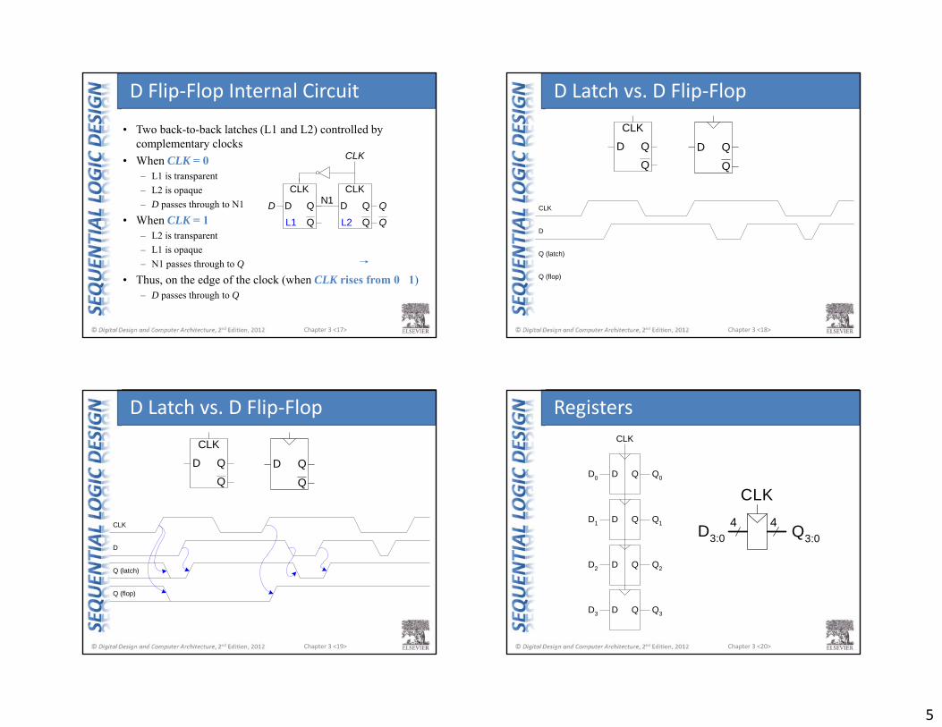
D Flip‐Flop Internal Circuit
Chapter 3 <18>
CLK
D Q
QD Q
Q
CLK
D
Q (latch)
Q (flop)
D Latch vs. D Flip‐Flop
Chapter 3 <19>
CLK
D
Q (latch)
Q (flop)
D Latch vs. D Flip‐Flop
CLK
D Q
QD Q
Q
Chapter 3 <20>
CLK
D Q
D Q
D Q
D Q
D0
D1
D2
D3
Q0
Q1
Q2
Q3
D3:04 4
CLK
Q3:0
Registers
6
Chapter 3 <21>
InternalCircuit
D Q
CLKEN
DQ
0
1D Q
EN
Symbol
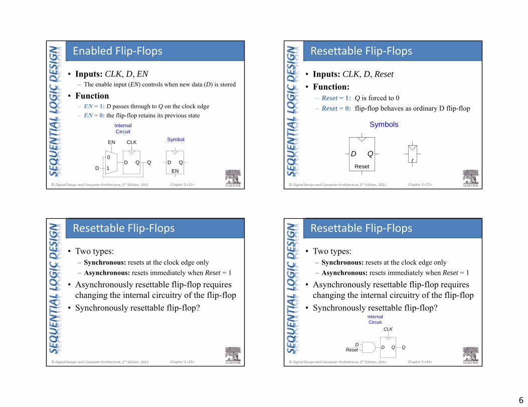
• Inputs: CLK, D, EN– The enable input (EN) controls when new data (D) is stored
• Function– EN = 1: D passes through to Q on the clock edge – EN = 0: the flip-flop retains its previous state
Enabled Flip‐Flops
Chapter 3 <22>
Symbols
D QReset
r
• Inputs: CLK, D, Reset• Function:
– Reset = 1: Q is forced to 0 – Reset = 0: flip-flop behaves as ordinary D flip-flop
Resettable Flip‐Flops
Chapter 3 <23>
• Two types:– Synchronous: resets at the clock edge only– Asynchronous: resets immediately when Reset = 1
• Asynchronously resettable flip-flop requires changing the internal circuitry of the flip-flop
• Synchronously resettable flip-flop?
Resettable Flip‐Flops
Chapter 3 <24>
• Two types:– Synchronous: resets at the clock edge only– Asynchronous: resets immediately when Reset = 1
• Asynchronously resettable flip-flop requires changing the internal circuitry of the flip-flop
• Synchronously resettable flip-flop?
Resettable Flip‐Flops
InternalCircuit
D Q
CLK
D QReset
7
Chapter 3 <25>
Symbols
D QSet
s
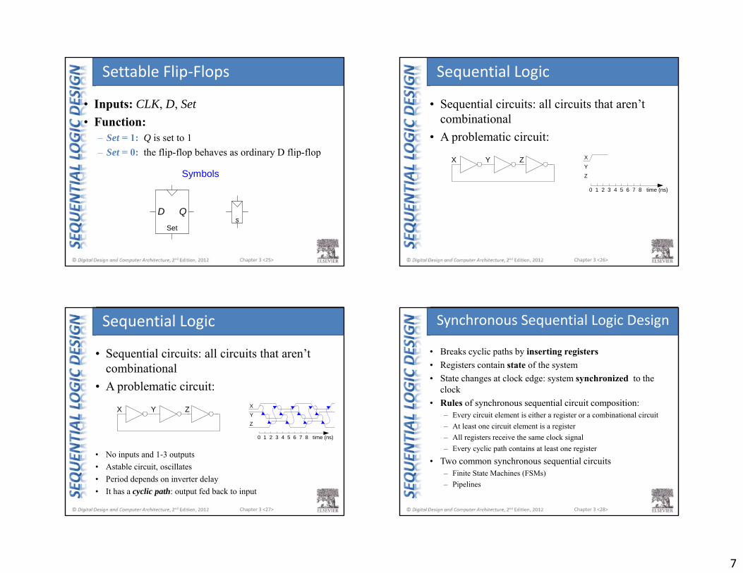
• Inputs: CLK, D, Set• Function:
– Set = 1: Q is set to 1 – Set = 0: the flip-flop behaves as ordinary D flip-flop
Settable Flip‐Flops
Chapter 3 <26>
X
Y
Z
time (ns)0 1 2 3 4 5 6 7 8
X Y Z
• Sequential circuits: all circuits that aren’t combinational
• A problematic circuit:
Sequential Logic
Chapter 3 <27>
X Y Z
• Sequential circuits: all circuits that aren’t combinational
• A problematic circuit:
• No inputs and 1-3 outputs• Astable circuit, oscillates• Period depends on inverter delay• It has a cyclic path: output fed back to input
Sequential Logic
X
Y
Z
time (ns)0 1 2 3 4 5 6 7 8
Chapter 3 <28>
• Breaks cyclic paths by inserting registers• Registers contain state of the system• State changes at clock edge: system synchronized to the
clock• Rules of synchronous sequential circuit composition:
– Every circuit element is either a register or a combinational circuit– At least one circuit element is a register– All registers receive the same clock signal– Every cyclic path contains at least one register
• Two common synchronous sequential circuits– Finite State Machines (FSMs)– Pipelines
Synchronous Sequential Logic Design
8
Chapter 3 <29>
NextState
CurrentState
S’ S
CLK
CL
Next StateLogic
NextState CL
OutputLogic
Outputs
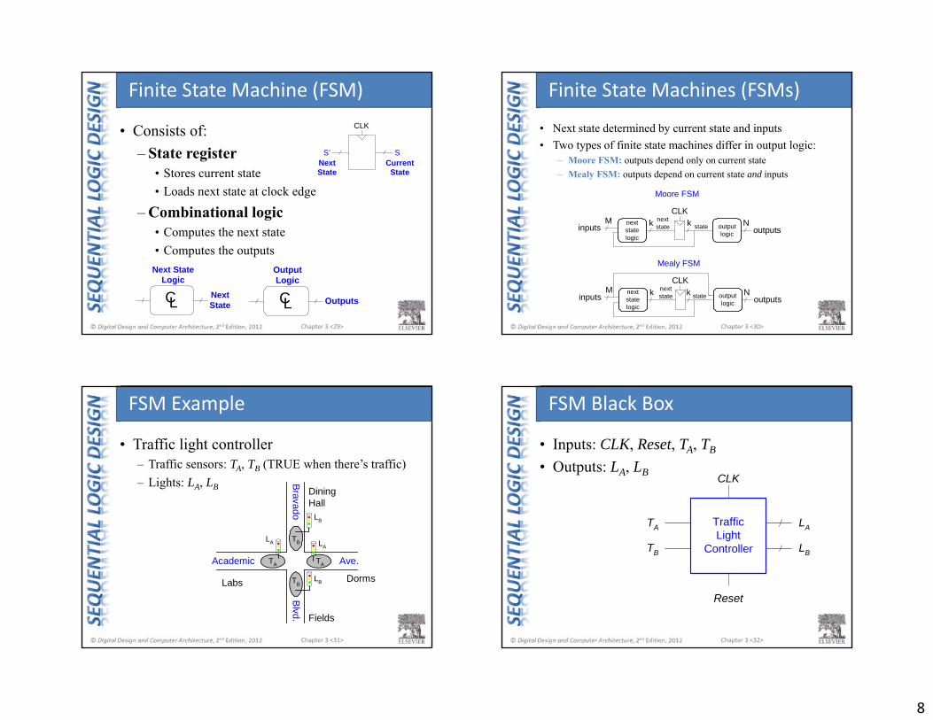
• Consists of:– State register
• Stores current state • Loads next state at clock edge
– Combinational logic• Computes the next state• Computes the outputs
Finite State Machine (FSM)
Chapter 3 <30>
CLKM Nk knext
statelogic
outputlogic
Moore FSM
CLKM Nk knext
statelogic
outputlogic
inputs
inputs
outputs
outputsstate
statenextstate
nextstate
Mealy FSM
• Next state determined by current state and inputs• Two types of finite state machines differ in output logic:
– Moore FSM: outputs depend only on current state– Mealy FSM: outputs depend on current state and inputs
Finite State Machines (FSMs)
Chapter 3 <31>
TA
LA
TA
LB
TB
TB
LA
LB
Academic Ave.
BravadoBlvd.
Dorms
Fields
DiningHall
Labs
• Traffic light controller– Traffic sensors: TA, TB (TRUE when there’s traffic)– Lights: LA, LB
FSM Example
Chapter 3 <32>
TA
TB
LA
LB
CLK
Reset
TrafficLight
Controller
• Inputs: CLK, Reset, TA, TB
• Outputs: LA, LB
FSM Black Box
9
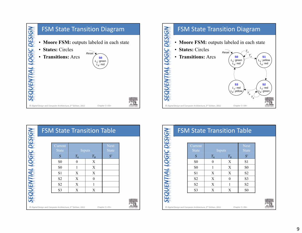
Chapter 3 <33>
S0LA: greenLB: red
Reset
• Moore FSM: outputs labeled in each state• States: Circles• Transitions: Arcs
FSM State Transition Diagram
Chapter 3 <34>
• Moore FSM: outputs labeled in each state• States: Circles• Transitions: Arcs
FSM State Transition Diagram
S0LA: greenLB: red
S1LA: yellow
LB: red
S3LA: red
LB: yellow
S2LA: red
LB: green
TA
TA
TB
TB
Reset
Chapter 3 <35>
Current State Inputs
Next State
S TA TB S'S0 0 XS0 1 XS1 X XS2 X 0S2 X 1S3 X X
FSM State Transition Table
Chapter 3 <36>
Current State Inputs
Next State
S TA TB S'S0 0 X S1S0 1 X S0S1 X X S2S2 X 0 S3S2 X 1 S2S3 X X S0
FSM State Transition Table
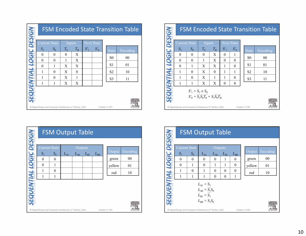
10
Chapter 3 <37>
Current State Inputs Next StateS1 S0 TA TB S'1 S'00 0 0 X0 0 1 X0 1 X X1 0 X 01 0 X 11 1 X X
State Encoding
S0 00
S1 01
S2 10
S3 11
FSM Encoded State Transition Table
Chapter 3 <38>
Current State Inputs Next StateS1 S0 TA TB S'1 S'00 0 0 X 0 10 0 1 X 0 00 1 X X 1 01 0 X 0 1 11 0 X 1 1 01 1 X X 0 0
State Encoding
S0 00
S1 01
S2 10
S3 11
S'1 = S1 S0
S'0 = S1S0TA + S1S0TB
FSM Encoded State Transition Table
Chapter 3 <39>
Current State OutputsS1 S0 LA1 LA0 LB1 LB0
0 00 11 01 1
Output Encoding
green 00
yellow 01
red 10
FSM Output Table
Chapter 3 <40>
Current State OutputsS1 S0 LA1 LA0 LB1 LB0
0 0 0 0 1 00 1 0 1 1 01 0 1 0 0 01 1 1 0 0 1
Output Encoding
green 00
yellow 01
red 10
LA1 = S1
LA0 = S1S0
LB1 = S1
LB0 = S1S0
FSM Output Table
11
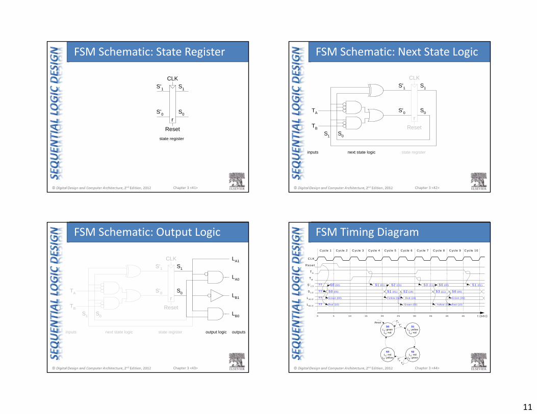
Chapter 3 <41>
S1
S0
S'1
S'0
CLK
state register
Reset
r
FSM Schematic: State Register
Chapter 3 <42>
S1
S0
S'1
S'0
CLK
next state logic state register
Reset
TA
TB
inputs
S1 S0
r
FSM Schematic: Next State Logic
Chapter 3 <43>
S1
S0
S'1
S'0
CLK
next state logic output logicstate register
Reset
LA1
LB1
LB0
LA0
TA
TB
inputs outputs
S1 S0
r
FSM Schematic: Output Logic
Chapter 3 <44>
C LK
R eset
T A
T B
S '1:0
S 1:0
L A1:0
L B1:0
C yc le 1 C yc le 2 C yc le 3 C yc le 4 C yc le 5 C yc le 6 C yc le 7 C yc le 8 C yc le 9 C yc le 10
S 1 (01 ) S 2 (10 ) S 3 (11 ) S 0 (00 )
t (sec )
??
??
S 0 (00 )
S 0 (00 ) S 1 (0 1 ) S 2 (10 ) S 3 (11 ) S 1 (01 )
??
??
0 5 10 15 20 2 5 30 3 5 40 45
G reen (00 )
R ed (1 0 )
S 0 (00 )
Y e llow (01 ) R e d (10 ) G reen (00 )
G reen (00 ) R ed (1 0 )Ye llow (01 )
S0LA: greenLB: red
S1LA: yellow
LB: red
S3LA: red
LB: yellow
S2LA: red
LB: green
TA
TA
TB
TB
Reset
FSM Timing Diagram
12
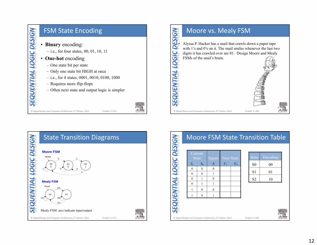
Chapter 3 <45>
• Binary encoding: – i.e., for four states, 00, 01, 10, 11
• One-hot encoding– One state bit per state– Only one state bit HIGH at once– i.e., for 4 states, 0001, 0010, 0100, 1000– Requires more flip-flops– Often next state and output logic is simpler
FSM State Encoding
Chapter 3 <46>
• Alyssa P. Hacker has a snail that crawls down a paper tape with 1’s and 0’s on it. The snail smiles whenever the last two digits it has crawled over are 01. Design Moore and Mealy FSMs of the snail’s brain.
Moore vs. Mealy FSM
Chapter 3 <47>
Mealy FSM: arcs indicate input/output
State Transition Diagrams
Moore FSMReset
S00
S10
S21
0
0 1
1 01
Reset
S0 S1
1/1
0/0
1/0 0/0
Mealy FSM
Chapter 3 <48>
Current State Inputs Next State
S1 S0 A S'1 S'00 0 00 0 10 1 00 1 1
1 0 0
1 0 1
State Encoding
S0 00
S1 01
S2 10
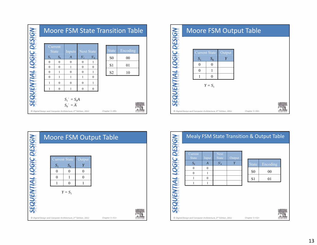
Moore FSM State Transition Table
13
Chapter 3 <49>
Current State Inputs Next State
S1 S0 A S'1 S'00 0 0 0 10 0 1 0 00 1 0 0 10 1 1 1 0
1 0 0 0 1
1 0 1 0 0
State Encoding
S0 00
S1 01
S2 10
Moore FSM State Transition Table
S1’ = S0A
S0’ = A
Chapter 3 <50>
Current State OutputS1 S0 Y0 00 11 0
Y = S1
Moore FSM Output Table
Chapter 3 <51>
Current State OutputS1 S0 Y0 0 00 1 01 0 1
Y = S1
Moore FSM Output Table
Chapter 3 <52>
Current State Input
Next State Output
S0 A S'0 Y0 00 11 01 1
State Encoding
S0 00
S1 01
Mealy FSM State Transition & Output Table
14
Chapter 3 <53>
Current State Input
Next State Output
S0 A S'0 Y0 0 1 00 1 0 01 0 1 01 1 0 1
State Encoding
S0 00
S1 01
Mealy FSM State Transition & Output Table
Chapter 3 <54>
Moore FSM Schematic
Y
CLK
Reset
A
r
S'0 S0
S'1 S1
Chapter 3 <55>
Mealy FSM Schematic
S'0 Y
CLK
Reset
A
r
S0
Chapter 3 <56>
Moore & Mealy Timing Diagram
Mealy Machine
Moore Machine
CLK
Reset
A
S
Y
S
Y
Cycle 1 Cycle 2 Cycle 3 Cycle 4 Cycle 5 Cycle 6 Cycle 7 Cycle 8 Cycle 9 Cycle 10
S0 S2?? S2 S2S0 S1
1 0 1 1 0 1 1 10
S1
S0 S0?? S0 S1 S0S1
S1 S0
S1
Cycle 11
15
Chapter 3 <57>
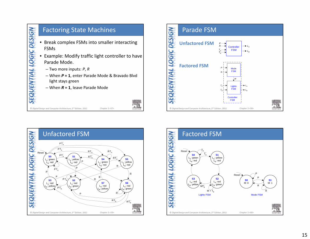
• Break complex FSMs into smaller interacting FSMs
• Example: Modify traffic light controller to have Parade Mode.– Two more inputs: P, R– When P = 1, enter Parade Mode & Bravado Blvd light stays green
– When R = 1, leave Parade Mode
Factoring State Machines
Chapter 3 <58>
Unfactored FSM
Factored FSM
ControllerFSMTA
TB
LA
LB
PR
ModeFSM
LightsFSM
P
M
ControllerFSM
TA
TB
LA
LB
R
Parade FSM
Chapter 3 <59>
S0LA: greenLB: red
S1LA: yellow
LB: red
S3LA: red
LB: yellow
S2LA: red
LB: green
TA
TA
TB
TB
Reset
S4LA: green
LB: red
S5LA: yellow
LB: red
S7LA: red
LB: yellow
S6LA: red
LB: green
TA
TA
P
P P
P
P
P
R
R
R
R
R
P
RP
TAP
TAP
P
TAR
TAR
R
TBRTBR
Unfactored FSM
Chapter 3 <60>
S0LA: greenLB: red
S1LA: yellow
LB: red
S3LA: red
LB: yellow
S2LA: red
LB: green
TA
TA
M + TB
MTB
Reset
Lights FSM
S0M: 0
S1M: 1
PReset P
Mode FSM
R
R
Factored FSM
16
Chapter 3 <61>
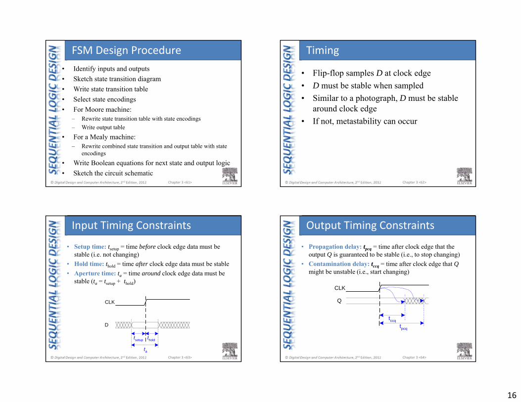
• Identify inputs and outputs• Sketch state transition diagram• Write state transition table• Select state encodings• For Moore machine:
– Rewrite state transition table with state encodings– Write output table
• For a Mealy machine:– Rewrite combined state transition and output table with state
encodings
• Write Boolean equations for next state and output logic• Sketch the circuit schematic
FSM Design Procedure
Chapter 3 <62>
• Flip-flop samples D at clock edge• D must be stable when sampled• Similar to a photograph, D must be stable
around clock edge• If not, metastability can occur
Timing
Chapter 3 <63>
CLK
tsetup
D
thold
ta
• Setup time: tsetup = time before clock edge data must be stable (i.e. not changing)
• Hold time: thold = time after clock edge data must be stable• Aperture time: ta = time around clock edge data must be
stable (ta = tsetup + thold)
Input Timing Constraints
Chapter 3 <64>
CLK
tccqtpcq
Q
• Propagation delay: tpcq = time after clock edge that the output Q is guaranteed to be stable (i.e., to stop changing)
• Contamination delay: tccq = time after clock edge that Qmight be unstable (i.e., start changing)
Output Timing Constraints
17
Chapter 3 <65>
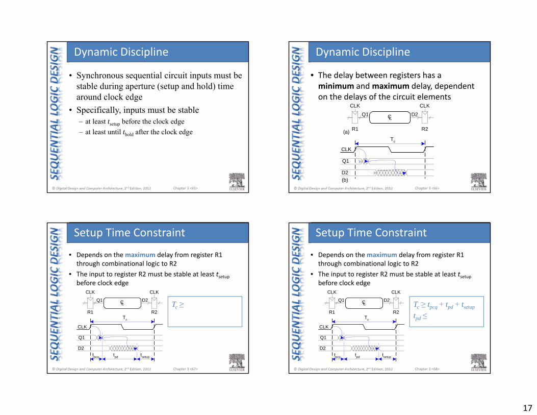
• Synchronous sequential circuit inputs must be stable during aperture (setup and hold) time around clock edge
• Specifically, inputs must be stable– at least tsetup before the clock edge– at least until thold after the clock edge
Dynamic Discipline
Chapter 3 <66>
• The delay between registers has a minimum and maximum delay, dependent on the delays of the circuit elements
CL
CLKCLK
R1 R2
Q1 D2
(a)
CLK
Q1
D2(b)
Tc
Dynamic Discipline
Chapter 3 <67>
• Depends on the maximum delay from register R1 through combinational logic to R2
• The input to register R2 must be stable at least tsetupbefore clock edge
CLK
Q1
D2
Tc
tpcq tpd tsetup
CL
CLKCLK
Q1 D2
R1 R2Tc ≥
Setup Time Constraint
Chapter 3 <68>
• Depends on the maximum delay from register R1 through combinational logic to R2
• The input to register R2 must be stable at least tsetupbefore clock edge
CLK
Q1
D2
Tc
tpcq tpd tsetup
CL
CLKCLK
Q1 D2
R1 R2Tc ≥ tpcq + tpd + tsetup
tpd ≤
Setup Time Constraint
18
Chapter 3 <69>
• Depends on the maximum delay from register R1 through combinational logic to R2
• The input to register R2 must be stable at least tsetupbefore clock edge
CLK
Q1
D2
Tc
tpcq tpd tsetup
CL
CLKCLK
Q1 D2
R1 R2Tc ≥ tpcq + tpd + tsetup
tpd ≤ Tc – (tpcq + tsetup)
Setup Time Constraint
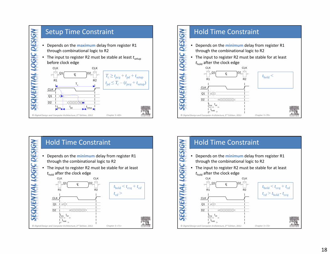
Chapter 3 <70>
• Depends on the minimum delay from register R1 through the combinational logic to R2
• The input to register R2 must be stable for at least thold after the clock edge
CLK
Q1
D2
tccq tcd
thold
CL
CLKCLK
Q1 D2
R1 R2thold <
Hold Time Constraint
Chapter 3 <71>
• Depends on the minimum delay from register R1 through the combinational logic to R2
• The input to register R2 must be stable for at least thold after the clock edge
CLK
Q1
D2
tccq tcd
thold
CL
CLKCLK
Q1 D2
R1 R2thold < tccq + tcd
tcd >
Hold Time Constraint
Chapter 3 <72>
• Depends on the minimum delay from register R1 through the combinational logic to R2
• The input to register R2 must be stable for at least thold after the clock edge
CLK
Q1
D2
tccq tcd
thold
CL
CLKCLK
Q1 D2
R1 R2thold < tccq + tcd
tcd > thold - tccq
Hold Time Constraint
19
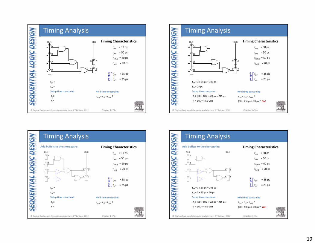
Chapter 3 <73>
CLK CLK
A
B
C
D
X'
Y'
X
Y
per g
ate
Timing Characteristicstccq = 30 ps
tpcq = 50 ps
tsetup = 60 ps
thold = 70 ps
tpd = 35 ps
tcd = 25 pstpd =
tcd =
Setup time constraint:
Tc ≥
fc =
Hold time constraint:
tccq + tcd > thold ?
Timing Analysis
Chapter 3 <74>
CLK CLK
A
B
C
D
X'
Y'
X
Y
per g
ate
Timing Characteristicstccq = 30 ps
tpcq = 50 ps
tsetup = 60 ps
thold = 70 ps
tpd = 35 ps
tcd = 25 pstpd = 3 x 35 ps = 105 ps
tcd = 25 ps
Setup time constraint:
Tc ≥ (50 + 105 + 60) ps = 215 ps
fc = 1/Tc = 4.65 GHz
Hold time constraint:
tccq + tcd > thold ?
(30 + 25) ps > 70 ps ? No!
Timing Analysis
Chapter 3 <75>
per g
ate
Timing Characteristicstccq = 30 ps
tpcq = 50 ps
tsetup = 60 ps
thold = 70 ps
tpd = 35 ps
tcd = 25 pstpd =
tcd =
Setup time constraint:
Tc ≥
fc =
Hold time constraint:
tccq + tcd > thold ?
Timing Analysis
CLK CLK
A
B
C
D
X'
Y'
X
Y
Add buffers to the short paths:
Chapter 3 <76>
per g
ate
Timing Characteristicstccq = 30 ps
tpcq = 50 ps
tsetup = 60 ps
thold = 70 ps
tpd = 35 ps
tcd = 25 pstpd = 3 x 35 ps = 105 ps
tcd = 2 x 25 ps = 50 ps
Setup time constraint:
Tc ≥ (50 + 105 + 60) ps = 215 ps
fc = 1/Tc = 4.65 GHz
Hold time constraint:
tccq + tcd > thold ?
(30 + 50) ps > 70 ps ? Yes!
Timing Analysis
CLK CLK
A
B
C
D
X'
Y'
X
Y
Add buffers to the short paths:
20
Chapter 3 <77>
• The clock doesn’t arrive at all registers at same time• Skew: difference between two clock edges• Perform worst case analysis to guarantee dynamic
discipline is not violated for any register – many registers in a system!
t skew
CLK1
CLK2
CL
CLK2CLK1
R1 R2
Q1 D2
CLKdelay
CLK
Clock Skew
Chapter 3 <78>
• In the worst case, CLK2 is earlier than CLK1
CLK1
Q1
D2
Tc
tpcq tpd tsetuptskew
CL
CLK2CLK1
R1 R2
Q1 D2
CLK2Tc ≥
Setup Time Constraint with Skew
Chapter 3 <79>
• In the worst case, CLK2 is earlier than CLK1
CLK1
Q1
D2
Tc
tpcq tpd tsetuptskew
CL
CLK2CLK1
R1 R2
Q1 D2
CLK2Tc ≥ tpcq + tpd + tsetup + tskew
tpd ≤
Setup Time Constraint with Skew
Chapter 3 <80>
• In the worst case, CLK2 is earlier than CLK1
CLK1
Q1
D2
Tc
tpcq tpd tsetuptskew
CL
CLK2CLK1
R1 R2
Q1 D2
CLK2Tc ≥ tpcq + tpd + tsetup + tskew
tpd ≤ Tc – (tpcq + tsetup + tskew)
Setup Time Constraint with Skew
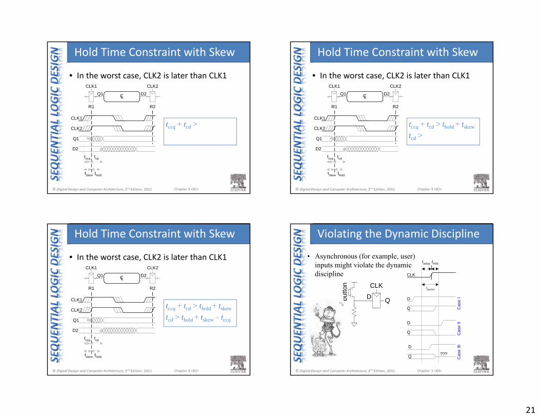
21
Chapter 3 <81>
• In the worst case, CLK2 is later than CLK1
tccq tcd
thold
Q1
D2
tskew
CL
CLK2CLK1
R1 R2
Q1 D2
CLK2
CLK1tccq + tcd >
Hold Time Constraint with Skew
Chapter 3 <82>
• In the worst case, CLK2 is later than CLK1
tccq tcd
thold
Q1
D2
tskew
CL
CLK2CLK1
R1 R2
Q1 D2
CLK2
CLK1tccq + tcd > thold + tskew
tcd >
Hold Time Constraint with Skew
Chapter 3 <83>
• In the worst case, CLK2 is later than CLK1
tccq tcd
thold
Q1
D2
tskew
CL
CLK2CLK1
R1 R2
Q1 D2
CLK2
CLK1tccq + tcd > thold + tskew
tcd > thold + tskew – tccq
Hold Time Constraint with Skew
Chapter 3 <84>
CLK
tsetup thold
taperture
D
Q
D
Q
D
Q ???
Cas
e I
Cas
e II
Cas
e III
D Q
CLK
butto
n
• Asynchronous (for example, user) inputs might violate the dynamic discipline
Violating the Dynamic Discipline
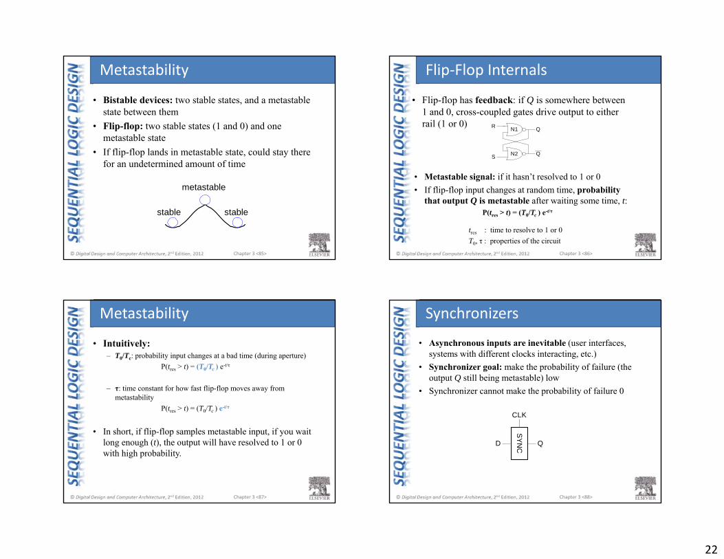
22
Chapter 3 <85>
metastable
stablestable
• Bistable devices: two stable states, and a metastable state between them
• Flip-flop: two stable states (1 and 0) and one metastable state
• If flip-flop lands in metastable state, could stay there for an undetermined amount of time
Metastability
Chapter 3 <86>
R
S
Q
Q
N1
N2
• Flip-flop has feedback: if Q is somewhere between 1 and 0, cross-coupled gates drive output to either rail (1 or 0)
• Metastable signal: if it hasn’t resolved to 1 or 0• If flip-flop input changes at random time, probability
that output Q is metastable after waiting some time, t:P(tres > t) = (T0/Tc ) e-t/τ
tres : time to resolve to 1 or 0T0, τ : properties of the circuit
Flip‐Flop Internals
Chapter 3 <87>
• Intuitively:– T0/Tc: probability input changes at a bad time (during aperture)
P(tres > t) = (T0/Tc ) e-t/τ
– τ: time constant for how fast flip-flop moves away from metastability
P(tres > t) = (T0/Tc ) e-t/τ
• In short, if flip-flop samples metastable input, if you wait long enough (t), the output will have resolved to 1 or 0 with high probability.
Metastability
Chapter 3 <88>
D Q
CLK
SY
NC
• Asynchronous inputs are inevitable (user interfaces, systems with different clocks interacting, etc.)
• Synchronizer goal: make the probability of failure (the output Q still being metastable) low
• Synchronizer cannot make the probability of failure 0
Synchronizers
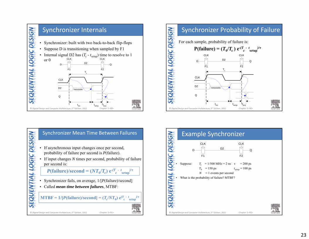
23
Chapter 3 <89>
D
Q
D2 Q
D2
Tc
tsetup tpcq
CLK CLK
CLK
tres
metastable
F1 F2
• Synchronizer: built with two back-to-back flip-flops• Suppose D is transitioning when sampled by F1• Internal signal D2 has (Tc - tsetup) time to resolve to 1
or 0
Synchronizer Internals
Chapter 3 <90>
D
Q
D2 Q
D2
Tc
tsetup tpcq
CLK CLK
CLK
tres
metastable
F1 F2
For each sample, probability of failure is:
P(failure) = (T0/Tc ) e-(Tc
- tsetup
)/τ
Synchronizer Probability of Failure
Chapter 3 <91>
• If asynchronous input changes once per second, probability of failure per second is P(failure).
• If input changes N times per second, probability of failure per second is:
P(failure)/second = (NT0/Tc) e-(Tc
- tsetup
)/τ
• Synchronizer fails, on average, 1/[P(failure)/second]• Called mean time between failures, MTBF:
MTBF = 1/[P(failure)/second] = (Tc/NT0) e(Tc
- tsetup
)/τ
Synchronizer Mean Time Between Failures
Chapter 3 <92>
D D2 Q
CLK CLK
F1 F2
• Suppose: Tc = 1/500 MHz = 2 ns τ = 200 psT0 = 150 ps tsetup = 100 psN = 1 events per second
• What is the probability of failure? MTBF?
Example Synchronizer
24
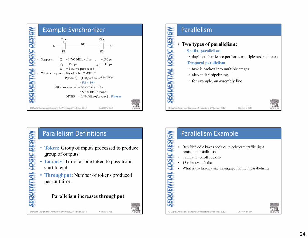
Chapter 3 <93>
D D2 Q
CLK CLK
F1 F2
• Suppose: Tc = 1/500 MHz = 2 ns τ = 200 psT0 = 150 ps tsetup = 100 psN = 1 events per second
• What is the probability of failure? MTBF?P(failure) = (150 ps/2 ns) e-(1.9 ns)/200 ps
= 5.6 × 10⁻⁶
P(failure)/second = 10 × (5.6 × 10-6 )= 5.6 × 10⁻⁵ / second
MTBF = 1/[P(failure)/second] ≈ 5 hours
Example Synchronizer
Chapter 3 <94>
• Two types of parallelism:– Spatial parallelism
• duplicate hardware performs multiple tasks at once– Temporal parallelism
• task is broken into multiple stages• also called pipelining• for example, an assembly line
Parallelism
Chapter 3 <95>
• Token: Group of inputs processed to produce group of outputs
• Latency: Time for one token to pass from start to end
• Throughput: Number of tokens produced per unit time
Parallelism increases throughput
Parallelism Definitions
Chapter 3 <96>
• Ben Bitdiddle bakes cookies to celebrate traffic light controller installation
• 5 minutes to roll cookies• 15 minutes to bake• What is the latency and throughput without parallelism?
Parallelism Example
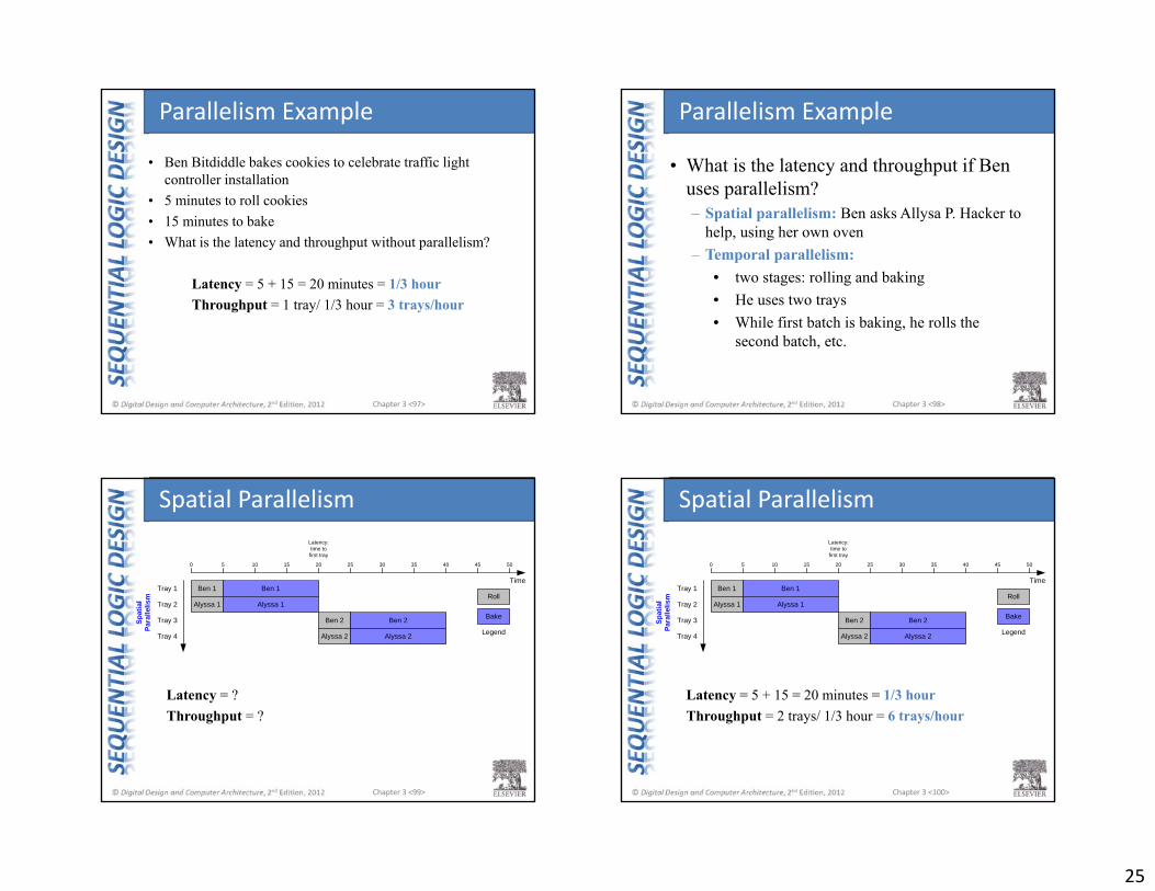
25
Chapter 3 <97>
• Ben Bitdiddle bakes cookies to celebrate traffic light controller installation
• 5 minutes to roll cookies• 15 minutes to bake• What is the latency and throughput without parallelism?
Latency = 5 + 15 = 20 minutes = 1/3 hourThroughput = 1 tray/ 1/3 hour = 3 trays/hour
Parallelism Example
Chapter 3 <98>
• What is the latency and throughput if Ben uses parallelism?– Spatial parallelism: Ben asks Allysa P. Hacker to
help, using her own oven– Temporal parallelism:
• two stages: rolling and baking • He uses two trays • While first batch is baking, he rolls the
second batch, etc.
Parallelism Example
Chapter 3 <99>
Latency = ?Throughput = ?
Spatial Parallelism
Spat
ial
Para
llelis
m Roll
Bake
Ben 1 Ben 1
Alyssa 1 Alyssa 1
Ben 2 Ben 2
Alyssa 2 Alyssa 2
Time
0 5 10 15 20 25 30 35 40 45 50
Tray 1
Tray 2
Tray 3
Tray 4
Latency:time to
first tray
Legend
Chapter 3 <100>
Latency = 5 + 15 = 20 minutes = 1/3 hourThroughput = 2 trays/ 1/3 hour = 6 trays/hour
Spatial Parallelism
Spat
ial
Para
llelis
m Roll
Bake
Ben 1 Ben 1
Alyssa 1 Alyssa 1
Ben 2 Ben 2
Alyssa 2 Alyssa 2
Time
0 5 10 15 20 25 30 35 40 45 50
Tray 1
Tray 2
Tray 3
Tray 4
Latency:time to
first tray
Legend
26
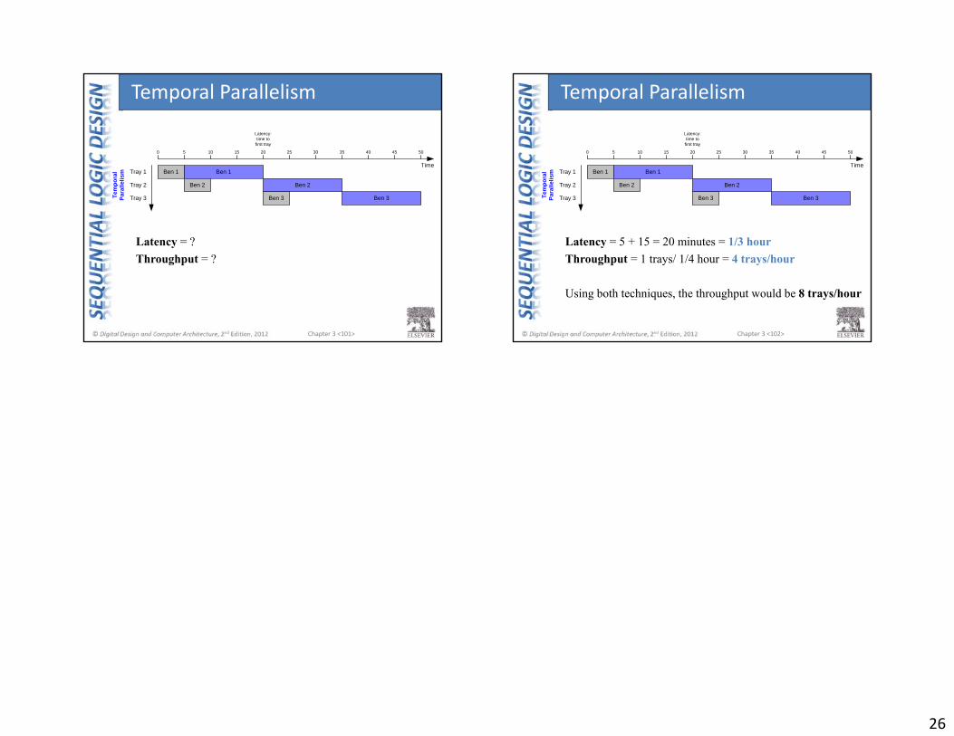
Chapter 3 <101>
Tem
pora
lPa
ralle
lism Ben 1 Ben 1
Ben 2 Ben 2
Ben 3 Ben 3
Time
0 5 10 15 20 25 30 35 40 45 50
Latency:time to
first tray
Tray 1
Tray 2
Tray 3
Latency = ?Throughput = ?
Temporal Parallelism
Chapter 3 <102>
Tem
pora
lPa
ralle
lism Ben 1 Ben 1
Ben 2 Ben 2
Ben 3 Ben 3
Time
0 5 10 15 20 25 30 35 40 45 50
Latency:time to
first tray
Tray 1
Tray 2
Tray 3
Latency = 5 + 15 = 20 minutes = 1/3 hourThroughput = 1 trays/ 1/4 hour = 4 trays/hour
Using both techniques, the throughput would be 8 trays/hour
Temporal Parallelism