Chapter 2 Design and Fabrication of VLSI Devicescadlab.cs.ucla.edu/~cong/CS258F/chap2.pdf · CS...
16
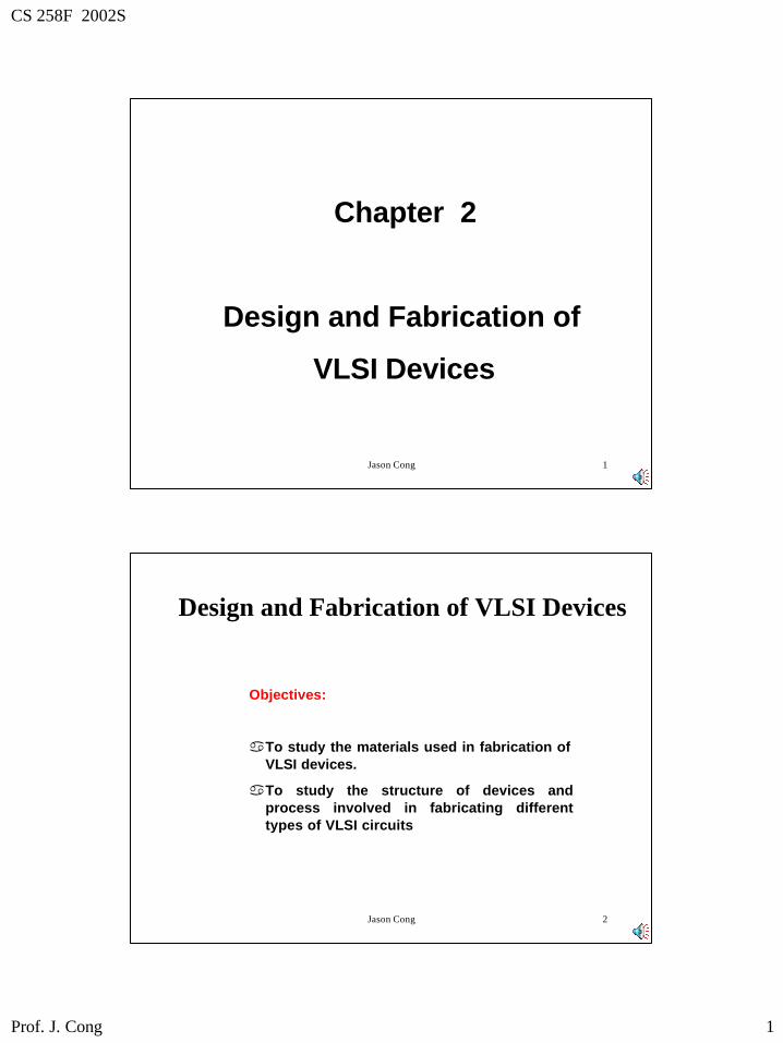
CS 258F 2002S Prof. J. Cong 1 Jason Cong 1 Chapter 2 Design and Fabrication of VLSI Devices Jason Cong 2 Design and Fabrication of VLSI Devices Objectives: aTo study the materials used in fabrication of VLSI devices. aTo study the structure of devices and process involved in fabricating different types of VLSI circuits
Transcript of Chapter 2 Design and Fabrication of VLSI Devicescadlab.cs.ucla.edu/~cong/CS258F/chap2.pdf · CS...
CS 258F 2002S
Prof. J. Cong 1
Jason Cong 1
Chapter 2
Design and Fabrication of
VLSI Devices
Jason Cong 2
Design and Fabrication of VLSI Devices
Objectives:
aTo study the materials used in fabrication of VLSI devices.
aTo study the structure of devices and process involved in fabricating different types of VLSI circuits

CS 258F 2002S
Prof. J. Cong 2
Jason Cong 3
Fabrication Materials
Jason Cong 4
Electron and Holes
a Holes travel as do electrons
a Material can be enriched in holes or electrons by introducing impurities
a Holes in crystals can be enriched by embedding some boron atoms
a Electrons in Crystals can be enriched by embedding phosphorus atoms
Free Electron
Silicon atom
+Ion
Hole
CS 258F 2002S
Prof. J. Cong 3
Jason Cong 5
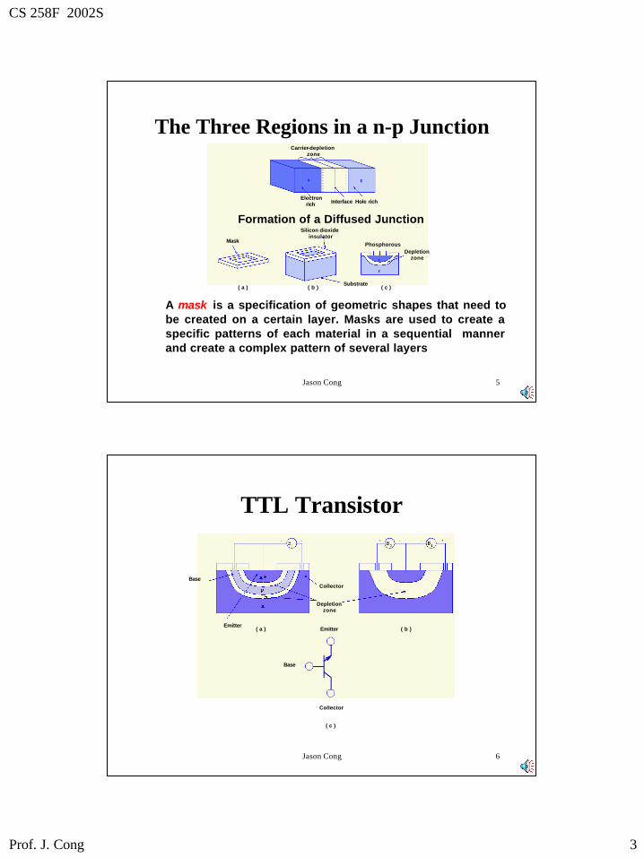
The Three Regions in a n-p Junction
A mask is a specification of geometric shapes that need to be created on a certain layer. Masks are used to create a specific patterns of each material in a sequential manner and create a complex pattern of several layers
Electron rich Interface Hole rich
Carrier-depletion zone
Mask
Silicon dioxide insulator
PhosphorousDepletion
zone
Substrate( a ) ( b ) ( c )
Formation of a Diffused Junction
Jason Cong 6
TTL Transistor
Collector
Depletion zone
Emitter
Base
( a ) ( b )Emitter
Base
Collector
( c )
CS 258F 2002S
Prof. J. Cong 4
Jason Cong 7
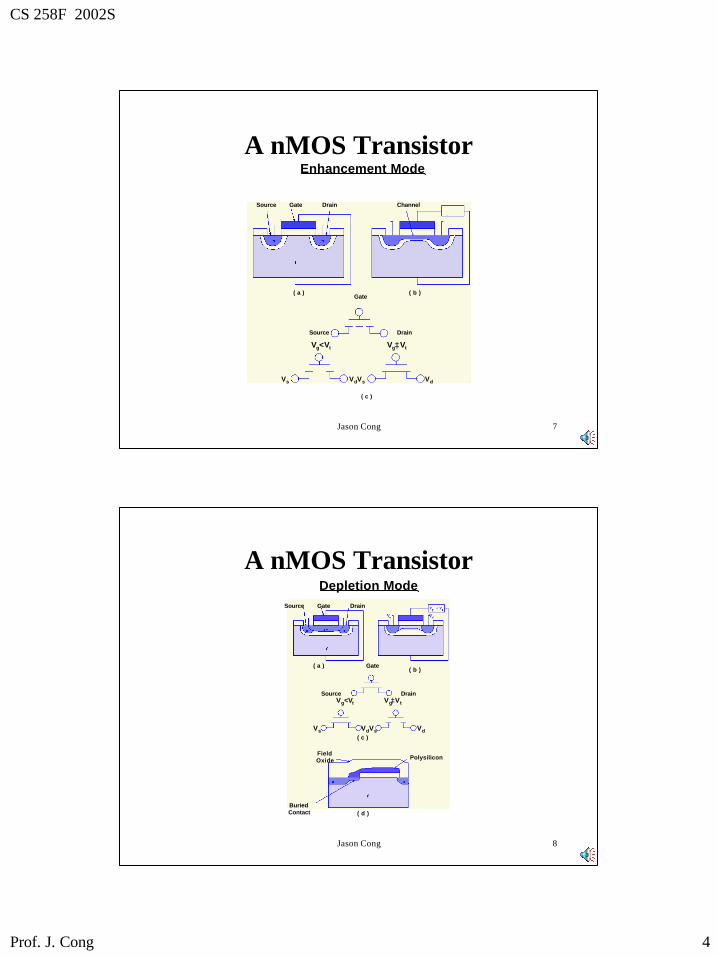
A nMOS TransistorEnhancement Mode
Source Gate Drain Channel
Gate
Source Drain
Vg<Vt Vg≥Vt
Vs VsVd Vd
( c )
( a ) ( b )
Jason Cong 8
A nMOS Transistor
( d )
Depletion ModeSource Gate Drain
Gate
Source DrainVg<Vt Vg≥Vt
Vs VsVd Vd
( a )( b )
( c )
PolysiliconField Oxide
Buried Contact
CS 258F 2002S
Prof. J. Cong 5
Jason Cong 9
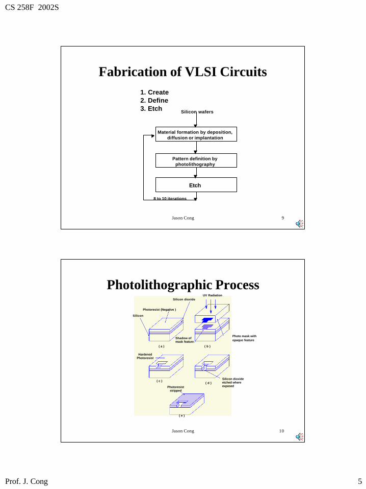
Fabrication of VLSI Circuits1. Create2. Define3. Etch
Material formation by deposition, diffusion or implantation
Pattern definition by photolithography
Etch
8 to 10 iterations
Silicon wafers
Jason Cong 10
Photolithographic Process
Photo mask with opaque feature
Silicon dioxide
Photoresist (Negative )
Silicon
Hardened Photoresist
Shadow of mask feature
Silicon dioxide etched where exposedPhotoresist
stripped
( a ) ( b )
( c )( d )
( e )
UV Radiation
CS 258F 2002S
Prof. J. Cong 6
Jason Cong 11
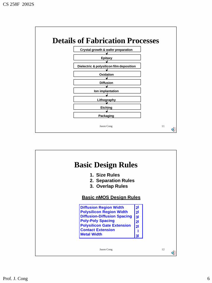
Details of Fabrication ProcessesCrystal growth & wafer preparation
Epitaxy
Dielectric & polysilicon film deposition
Oxidation
Diffusion
Ion implantation
Lithography
Etching
Packaging
Jason Cong 12
Basic Design Rules1. Size Rules2. Separation Rules3. Overlap Rules
Basic nMOS Design Rules
Diffusion Region WidthPolysilicon Region WidthDiffusion-Diffusion SpacingPoly-Poly SpacingPolysilicon Gate ExtensionContact ExtensionMetal Width
2λ2λ3λ2λ2λ λ3λ
CS 258F 2002S
Prof. J. Cong 7
Jason Cong 13
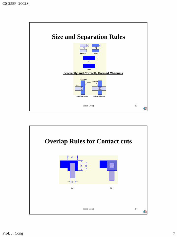
Size and Separation Rules
Incorrectly and Correctly Formed Channels
Diffusion
Short
Poly
Incorrectly formed
Channel
Correctly formed
Metal
Diffusion Poly
Jason Cong 14
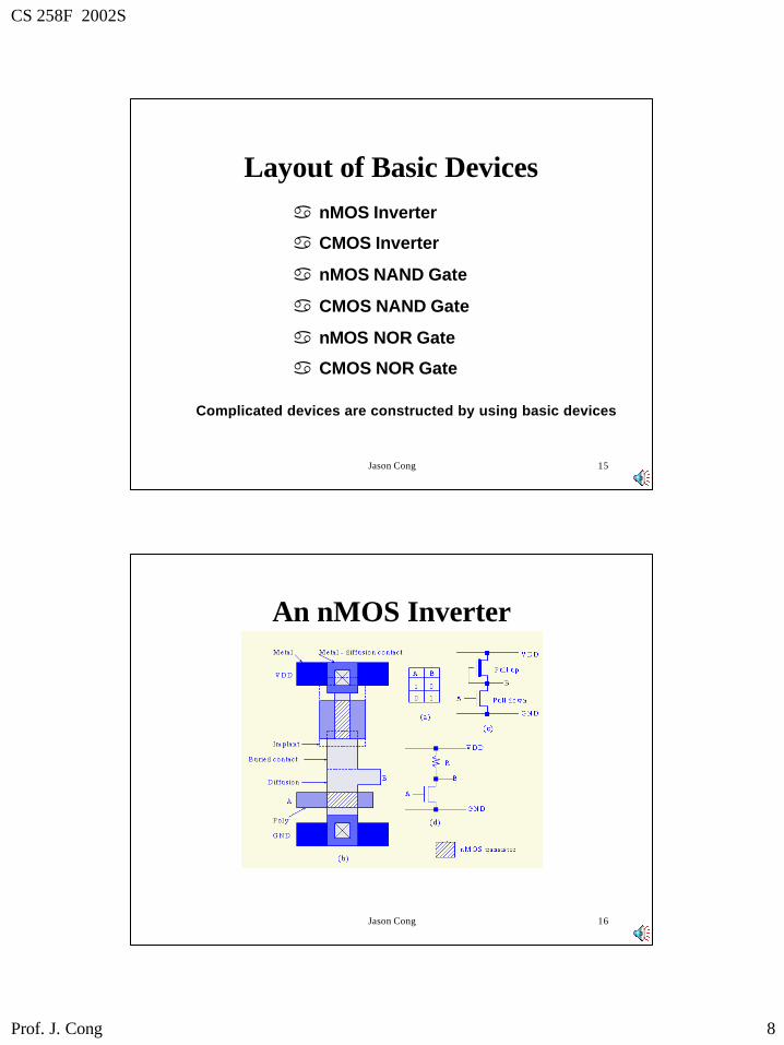
Overlap Rules for Contact cuts
( a ) ( b )
CS 258F 2002S
Prof. J. Cong 8
Jason Cong 15
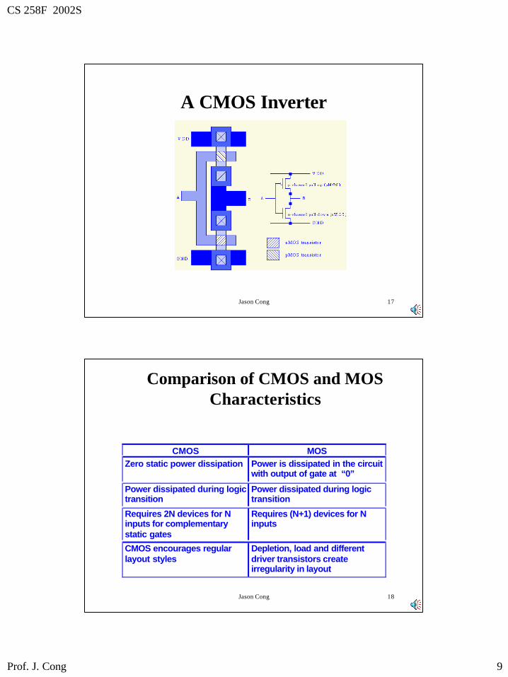
Layout of Basic Devicesa nMOS Inverter
a CMOS Inverter
a nMOS NAND Gate
a CMOS NAND Gate
a nMOS NOR Gate
a CMOS NOR Gate
Complicated devices are constructed by using basic devices
Jason Cong 16
An nMOS Inverter
CS 258F 2002S
Prof. J. Cong 9
Jason Cong 17
A CMOS Inverter
Jason Cong 18
Comparison of CMOS and MOS Characteristics
CMOS MOSZero static power dissipation Power is dissipated in the circuit
with output of gate at “0”
Power dissipated during logictransition
Power dissipated during logictransition
Requires 2N devices for Ninputs for complementarystatic gates
Requires (N+1) devices for Ninputs
CMOS encourages regularlayout styles
Depletion, load and differentdriver transistors createirregularity in layout
CS 258F 2002S
Prof. J. Cong 10
Jason Cong 19
A nMOS NAND Gate
Jason Cong 20
A CMOS NAND Gate
CS 258F 2002S
Prof. J. Cong 11
Jason Cong 21
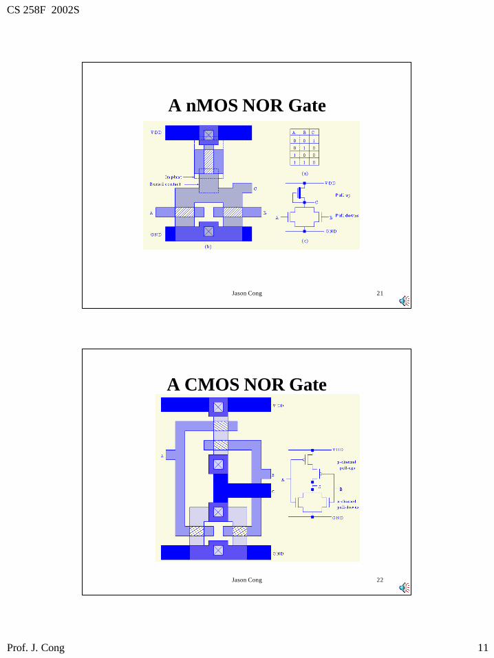
A nMOS NOR Gate
Jason Cong 22
A CMOS NOR Gate
CS 258F 2002S
Prof. J. Cong 12
Jason Cong 23
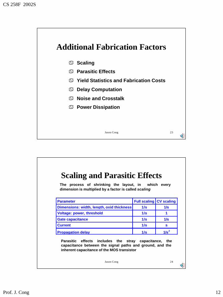
Additional Fabrication Factors
a Scaling
a Parasitic Effects
a Yield Statistics and Fabrication Costs
a Delay Computation
a Noise and Crosstalk
a Power Dissipation
Jason Cong 24
Scaling and Parasitic EffectsThe process of shrinking the layout, in which every dimension is multiplied by a factor is called scaling
Parasitic effects includes the stray capacitance, the capacitance between the signal paths and ground, and the inherent capacitance of the MOS transistor
Parameter Full scaling CV scaling
Dimensions: width, length, oxid thickness 1/s 1/s
Voltage: power, threshold 1/s 1
Gate capacitance 1/s 1/s
Current 1/s s
Propagation delay 1/s 1/s2
CS 258F 2002S
Prof. J. Cong 13
Jason Cong 25
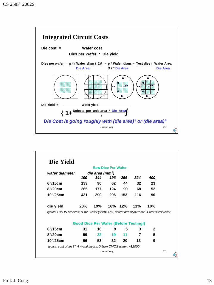
Defects_per_unit_area * Die_Areaα
α}
Integrated Circuit Costs
Die Cost is going roughly with (die area)3 or (die area)4
{ 1+
Die cost = Wafer cost
Dies per Wafer * Die yield
Dies per wafer = π * ( Wafer_diam / 2)2 – π * Wafer_diam – Test dies ≈ Wafer AreaDie Area √ 2 * Die Area Die Area
Die Yield = Wafer yield
Jason Cong 26
Die YieldRaw Dice Per Wafer
wafer diameter die area (mm2)100 144 196 256 324 400
6”/15cm 139 90 62 44 32 23 8”/20cm 265 177 124 90 68 52
10”/25cm 431 290 206 153 116 90
die yield 23% 19% 16% 12% 11% 10%typical CMOS process: α =2, wafer yield=90%, defect density=2/cm2, 4 test sites/wafer
Good Dice Per Wafer (Before Testing!)6”/15cm 31 16 9 5 3 2 8”/20cm 59 32 19 11 7 5
10”/25cm 96 53 32 20 13 9typical cost of an 8”, 4 metal layers, 0.5um CMOS wafer: ~$2000
CS 258F 2002S
Prof. J. Cong 14
Jason Cong 27
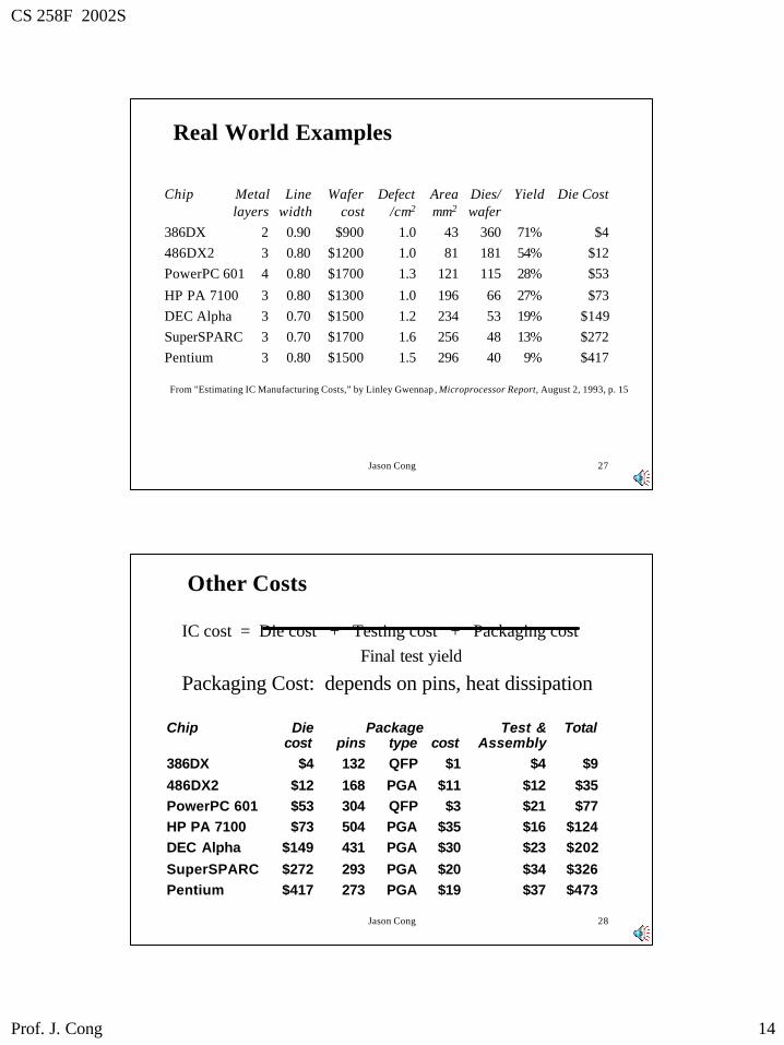
Real World Examples
Chip Metal Line Wafer Defect Area Dies/ Yield Die Costlayers width cost /cm2 mm2 wafer
386DX 2 0.90 $900 1.0 43 360 71% $4 486DX2 3 0.80 $1200 1.0 81 181 54% $12 PowerPC 601 4 0.80 $1700 1.3 121 115 28% $53
HP PA 7100 3 0.80 $1300 1.0 196 66 27% $73 DEC Alpha 3 0.70 $1500 1.2 234 53 19% $149SuperSPARC 3 0.70 $1700 1.6 256 48 13% $272 Pentium 3 0.80 $1500 1.5 296 40 9% $417
From "Estimating IC Manufacturing Costs,” by Linley Gwennap , Microprocessor Report, August 2, 1993, p. 15
Jason Cong 28
IC cost = Die cost + Testing cost + Packaging costFinal test yield
Packaging Cost: depends on pins, heat dissipation
Other Costs
Chip Die Package Test & Totalcost pins type cost Assembly
386DX $4 132 QFP $1 $4 $9
486DX2 $12 168 PGA $11 $12 $35 PowerPC 601 $53 304 QFP $3 $21 $77 HP PA 7100 $73 504 PGA $35 $16 $124 DEC Alpha $149 431 PGA $30 $23 $202
SuperSPARC $272 293 PGA $20 $34 $326 Pentium $417 273 PGA $19 $37 $473
CS 258F 2002S
Prof. J. Cong 15
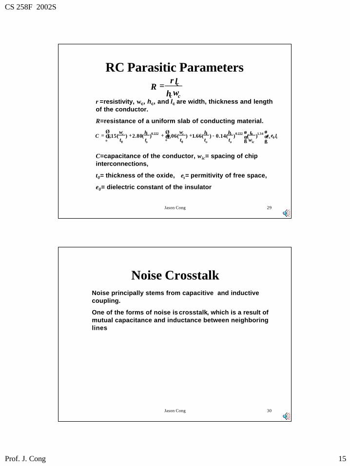
Jason Cong 29
RC Parasitic Parametersρ
cc
c
hl
Rω
=
csico
c
o
cc
o
cc lt
th
th
tth
tC 0
34.10222.0
0
222.0
0
)()(14.0)(66.1)(06.0)(80.2)(15.1 εεω
ωω
−+++=
ρ=resistivity, ωc, hc, and lc are width, thickness and length of the conductor.
R=resistance of a uniform slab of conducting material.
C=capacitance of the conductor, ωic= spacing of chip interconnections,
t0= thickness of the oxide, εs= permitivity of free space,
ε0= dielectric constant of the insulator
Jason Cong 30
Noise CrosstalkNoise principally stems from capacitive and inductive coupling.
One of the forms of noise is crosstalk, which is a result of mutual capacitance and inductance between neighboring lines
CS 258F 2002S
Prof. J. Cong 16
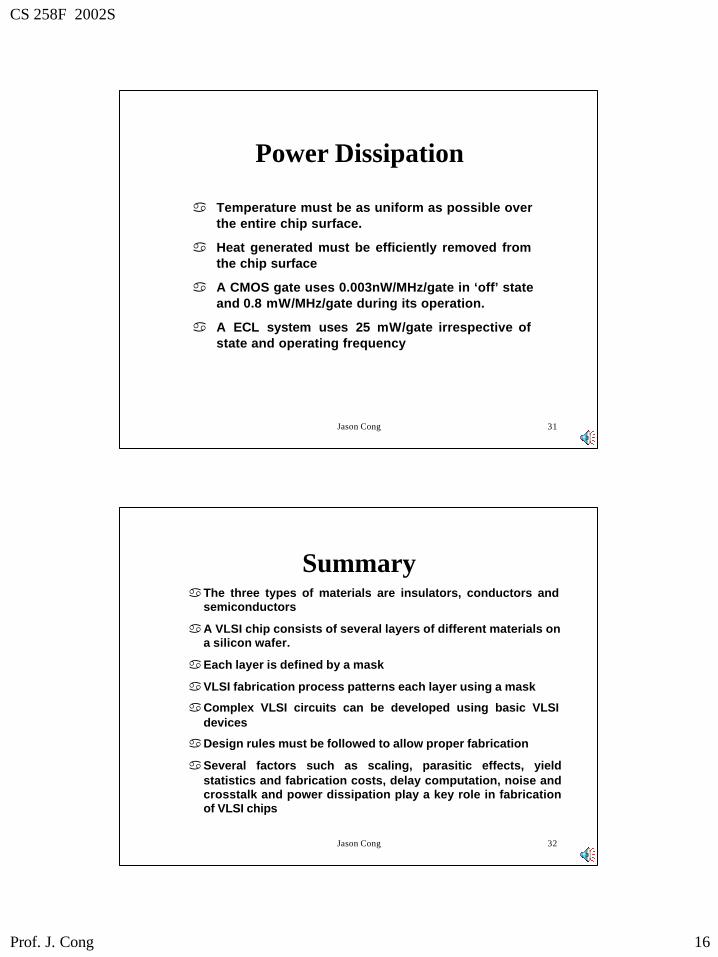
Jason Cong 31
Power Dissipation
a Temperature must be as uniform as possible over the entire chip surface.
a Heat generated must be efficiently removed from the chip surface
a A CMOS gate uses 0.003nW/MHz/gate in ‘off’ state and 0.8 mW/MHz/gate during its operation.
a A ECL system uses 25 mW/gate irrespective of state and operating frequency
Jason Cong 32
SummaryaThe three types of materials are insulators, conductors and
semiconductors
aA VLSI chip consists of several layers of different materials ona silicon wafer.
aEach layer is defined by a mask
aVLSI fabrication process patterns each layer using a mask
aComplex VLSI circuits can be developed using basic VLSI devices
aDesign rules must be followed to allow proper fabrication
aSeveral factors such as scaling, parasitic effects, yield statistics and fabrication costs, delay computation, noise and crosstalk and power dissipation play a key role in fabrication of VLSI chips