Chapter 16 CMOS Amplifiers 16.1 General Considerations 16.2 Operating Point Analysis and Design ...
94
Chapter 16 CMOS Amplifiers 16.1 General Considerations 16.2 Operating Point Analysis and Design 16.3 CMOS Amplifier Topologies 16.4 Common-Source Topology 16.5 Summary and Additional Examples 16.6 Chapter Summary 1
-
Upload
britton-simon -
Category
Documents
-
view
234 -
download
4
Transcript of Chapter 16 CMOS Amplifiers 16.1 General Considerations 16.2 Operating Point Analysis and Design ...

Chapter 16 CMOS Amplifiers
16.1 General Considerations 16.2 Operating Point Analysis and Design 16.3 CMOS Amplifier Topologies 16.4 Common-Source Topology 16.5 Summary and Additional Examples 16.6 Chapter Summary
1

Chapter Outline
2CH 16 CMOS Amplifiers

Example: Desired I/O Impedances
3CH 16 CMOS Amplifiers
inR 0ampR

Method to Measure the I/O Impedances
4CH 16 CMOS Amplifiers
To measure Rin(Rout), deactivate all the other independent sources in the circuit and find the ratio of vX/iX.
X
Xin i
vR
X
Xout i
vR

Example: Input Impedance of a Simple Amplifier
5CH 16 CMOS Amplifiers
inX Ri 0

The Concept of Impedance at a Node
6CH 16 CMOS Amplifiers
When the other node of a port is grounded, it is more convenient to use the concept of impedance at a node.

Example: Impedance Seen at Drain
7CH 16 CMOS Amplifiers
Oout rR

Example: Impedance Seen at Source
8CH 16 CMOS Amplifiers
mout g
R1
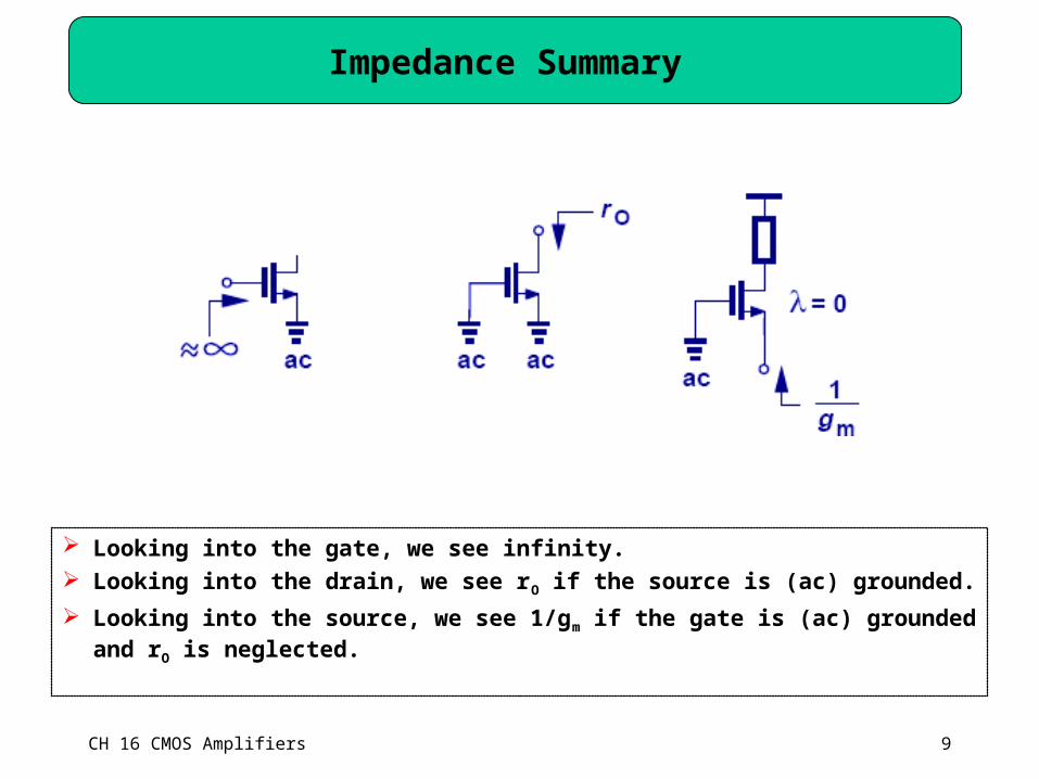
Impedance Summary
9CH 16 CMOS Amplifiers
Looking into the gate, we see infinity. Looking into the drain, we see rO if the source is (ac) grounded.
Looking into the source, we see 1/gm if the gate is (ac) grounded and rO is neglected.

Bias and Signal Levels for a MOS Transistor
10CH 16 CMOS Amplifiers
Bias point analysis establishes the region of operation and the small-signal parameters.
On top of the bias point, small signals are applied to the circuit.

General Steps in Circuit Analysis
11CH 16 CMOS Amplifiers
First, the effects of constant voltage/current sources are analyzed when signal sources are deactivated.
Second, small-signal analysis is done when constant sources are set to zero.

Simplification of Supply Voltage Notation
12CH 16 CMOS Amplifiers

Example: Amplifier Driven by a Microphone
13CH 16 CMOS Amplifiers
20mV
0V
Microphone Output
Since the DC (average) value is at zero, and 20mV is not sufficient to turn on M1, M1 is off and Vout is at VDD.

Example: Amplifier with Gate Tied to VDD
14CH 16 CMOS Amplifiers
Since the gate voltage level is fixed at VDD, no signal current will be produced my M1, leading to no amplification.

Example: Amplifier with Gate Bias
15CH 16 CMOS Amplifiers
With proper value of VB, M1 can operate in the desired saturation region and amplify the incoming voice signal.

Simple Biasing
16CH 16 CMOS Amplifiers
In (a), VGS=VDD, whereas in (b) VGS equals to a fraction of VDD.
DDGS VRR
RV
21
2

Example: Bias Current and Maximum RD
17CH 16 CMOS Amplifiers
KR
KR
LW
VAC
VV
oxn
TH
15
20
0
18.05
/100
5.0
2
1
2
KRVVVVV
AVVRR
R
L
WCI
DRDTHGSD
THDDoxnD
15529.1271.0
1022
1
maxmin
2
21
2

Capacitive Coupling
18CH 16 CMOS Amplifiers
Capacitive coupling is used to block the zero DC output value of the microphone and pass the voice signal to the amplifier.

Biasing with Source Degeneration
19CH 16 CMOS Amplifiers
Soxn
THDD
THGS
RLW
CV
VRR
VRVVVVV
1
2
1
21
21
211

Example: ID and Maximum RD for Source Degeneration Biasing
20CH 16 CMOS Amplifiers
0
18.0/5/
/100
5.02
LW
VAC
VV
oxn
TH
KI
VVVR
VVRR
VRVVVVV
VR
LW
CV
D
THXDDD
THDD
THGS
Soxn
25.3)(
974.02
36.01
21
21
211
1

Example: Maximum W/L and Minimum RS
21CH 16 CMOS Amplifiers
0
5.2
/100
5.02
KR
VAC
VV
D
oxn
TH
2.56
38.050406
max
2
2max
L
W
VL
W
V
AA
R
VVI
D
YDDD
604
041.12
minD
GSXS
oxn
DTHGS
I
VVR
V
LW
C
IVV

Self-Biased MOS Stage
22CH 16 CMOS Amplifiers
2
2
1THDDSDDoxnD VIRRV
L
WCI
The gate voltage is provided by the drain with no voltage drop across RG and M1 is always in saturation.
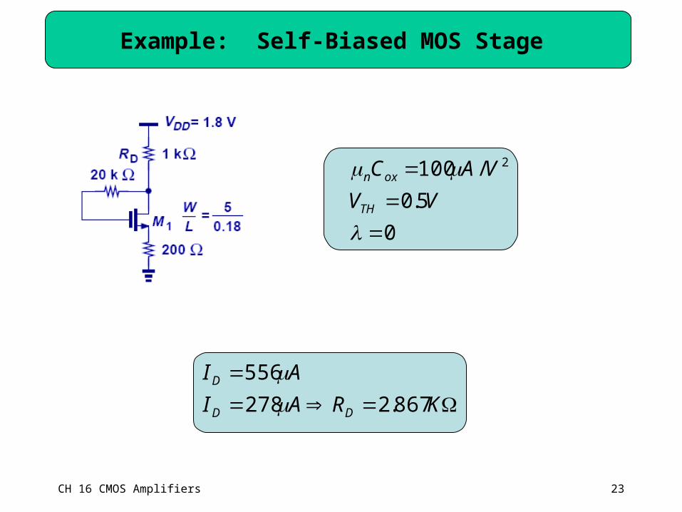
Example: Self-Biased MOS Stage
23CH 16 CMOS Amplifiers
0
5.0
/100 2
VV
VAC
TH
oxn
KRAI
AI
DD
D
867.2278
556

Example: PMOS Stage with Biasing
VV
KR
KR
LW
VAC
TH
oxp
5.0
15
20
0
18.05
/50
2
1
2
KRSaturation
AVVL
WCI
VVRR
RV
D
THGSoxpD
DDGS
3.27
562
1
771.0
max
2
21
2
24CH 16 CMOS Amplifiers

Example: PMOS Stage with Self-Biasing
VV
LW
VAC
TH
oxp
5.0
0
18.05
/50 2
AI
VRIVL
WCI
D
THDDDDoxpD
4182
1 2
25CH 16 CMOS Amplifiers

Good Example of Current Source
As long as a MOS transistor is in saturation region and λ=0, the current is independent of the drain voltage and it behaves as an ideal current source seen from the drain terminal.
26CH 16 CMOS Amplifiers

Bad Example of Current Source
Since the variation of the source voltage directly affects the current of a MOS transistor, it does not operate as a good current source if seen from the source terminal
27CH 16 CMOS Amplifiers

Possible I/O Connections to a MOS Transistor
Of all the possible I/O connections to a MOS transistor, only (a,d), (a,e) and (b,d) are functional.
28CH 16 CMOS Amplifiers

Common Source (CS) Stage
If the input is applied to the gate and the output is sensed at the drain, the circuit is called a “common-source” (CS) stage.
29CH 16 CMOS Amplifiers

Small-Signal Model of CS Stage
30CH 16 CMOS Amplifiers
Dmv
mD
out
RgA
vgR
v
1

Example: CS Stage
31
33.3300
12
Dmv
Doxnm
RgA
IL
WCg
CH 16 CMOS Amplifiers
0
5.0
/100
12
VV
VAC
mAI
TH
oxn
D
Saturation
VIRVVVV
V
LW
C
IVV
DDDDTHGS
oxn
DTHGS
6.08.0
8.0,6.0
1.12

Example: Faulty CS Stage Design
32CH 16 CMOS Amplifiers
0
18.05
/100
5.0
5
8.1
1
2
LW
VAC
VV
A
VV
mWPower
oxn
TH
v
DD
28455
56915561
Dv
mD
RA
gAImWPower
However, no solution exists since M1 is out of the saturation region (VDD-IDRD<VGS-VTH).

CS Stage I/O Impedance Calculation
x
xin i
vR
33CH 16 CMOS Amplifiers
Dx
xout R
i
vR

CS Stage Including Channel-Length Modulation
34CH 16 CMOS Amplifiers
ODout
ODmv
rRR
rRgA
||
||

xAv
Example: ½ Gain
2xAv
35CH 16 CMOS Amplifiers
No Channel-Length Modulation With Channel-Length Modulation
DD
DD
O
RI
RI
r
1
1

Example: RD → ∞
36CH 16 CMOS Amplifiers
D
oxn
D
oxn
v
Omv
I
WLC
ILW
CA
rgA
2
2

CS Stage with Current Source Load
37CH 16 CMOS Amplifiers
21
211
||
||
OOout
OOmv
rrR
rrgA

Example: CS Stage with Current Source Load
38CH 16 CMOS Amplifiers
211 || OOmv rrgA

CS Stage with Diode-Connected Load
39CH 16 CMOS Amplifiers
122
122
1
||||1
||||1
OOm
out
OOm
mv
rrg
R
rrg
gA

Example: CS Stage with Diode-Connected PMOS
40CH 16 CMOS Amplifiers
12
12 ||||
1OO
mmv rr
ggA

CS Stage with Source Degeneration
41CH 16 CMOS Amplifiers
Sm
Dv
Rg
RA
1

Example: CS Stage with Source Degeneration
42CH 16 CMOS Amplifiers
21
11
mm
Dv
gg
RA

Example: Degeneration Resistor
8
2001
v
m
A
g
4
2001
v
m
A
g
43CH 16 CMOS Amplifiers
200141
6.18
mSSm
Dm
DDm
gRRg
Rg
KRRg
Without Degeneration With Degeneration

Effective Transconductance
44CH 16 CMOS Amplifiers
Sm
m
in
outm Rg
g
v
iG
1

Effect of Transistor Output Resistance
45CH 16 CMOS Amplifiers
SmOout
SOmOout
RgrR
RrgrR
1
1

Stage with Explicit Depiction of rO
46CH 16 CMOS Amplifiers
Sometimes, the transistor’s output resistance is explicitly drawn to emphasize its significance.

Example: NMOS Current Source Design
VV
V
VAC
KR
mAI
DS
oxn
out
D
3.0
25.0
/100
20
1
min
1
2
47CH 16 CMOS Amplifiers
578
201
150
12
3.0min
S
SOSm
THGS
Dm
THGSDS
R
KRrRg
VV
Ig
VVV

Example: Output Resistance of CS Stage with Degeneration I
48CH 16 CMOS Amplifiers
121
2211
2
111
Ooutmmm
mmmOout
rRggg
gggrR

Example: Output Resistance of CS Stage with Degeneration II
49CH 16 CMOS Amplifiers
211
12111
OOmout
OOOmout
rrgR
rrrgR
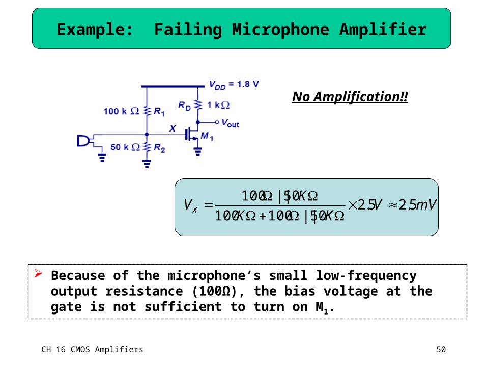
Example: Failing Microphone Amplifier
50CH 16 CMOS Amplifiers
No Amplification!!
Because of the microphone’s small low-frequency output resistance (100Ω), the bias voltage at the gate is not sufficient to turn on M1.
mVVKK
KVX 5.25.2
50||100100
50||100

Capacitive Coupling
51CH 16 CMOS Amplifiers
To fix the problem in the previous example, a method known as capacitive coupling is used to block the DC content of the microphone and pass the AC signal to the amplifier.

Capacitive Coupling: Bias Analysis
52CH 16 CMOS Amplifiers
Since a capacitor is an open at DC, it can be replaced by an open during bias point analysis.
2
21
2
2
1
THDDoxnD VV
RR
R
L
WCI

Capacitive Coupling: AC Analysis
53CH 16 CMOS Amplifiers
Since a capacitor is a short at AC, it can be replaced by a short during AC analysis.
ODmin
out rRgv
v||

Capacitive Coupling: I/O Impedances
212
1
|| RRR
R
in
in
54CH 16 CMOS Amplifiers
ODout rRR ||

Example: Amplifier with Direction Connection of Speaker
55CH 16 CMOS Amplifiers
This amplifier design still fails because the solenoid of the speaker shorts the drain to ground.

Example: Amplifier with Capacitive Coupling at I/O
56CH 16 CMOS Amplifiers
This amplifier design produces very little gain because its equivalent output resistance is too small.
08.0||
8||
spDmv
spDeq
RRgA
RRR

Source Degeneration with Bypass Capacitor
57CH 16 CMOS Amplifiers
It is possible to utilize degeneration for biasing but eliminate its effect on the small-signal by adding a bypass capacitor.
DmG
v RgRRR
RRA
21
21
||
||
Example: Source Degeneration with Bypass Capacitor Design
mVV
VV
VV
VAC
mWPower
KR
A
SR
DD
TH
oxn
in
v
400
8.1
0
5.0
/100
5
50
5
2
58CH 16 CMOS Amplifiers
KRKR
R
LW
g
R
D
m
S
225,3.64
2463
864
3.461
148
21

Concept Summary
59CH 16 CMOS Amplifiers

Common-Gate Stage
60CH 16 CMOS Amplifiers
In a common-gate stage, the input is applied at the source while the output is taken at the drain.

Small Signal Analysis of Common-Gate Stage
61CH 16 CMOS Amplifiers
Dmv RgA

Example: Common-Gate Stage Design
VV
VV
VAC
LW
mAI
DD
TH
oxn
D
8.1
5.0
/100
50
5.0
2
62CH 16 CMOS Amplifiers
06.64471
71.2
vm
DTHbDDDD
Ag
kRVVRIV
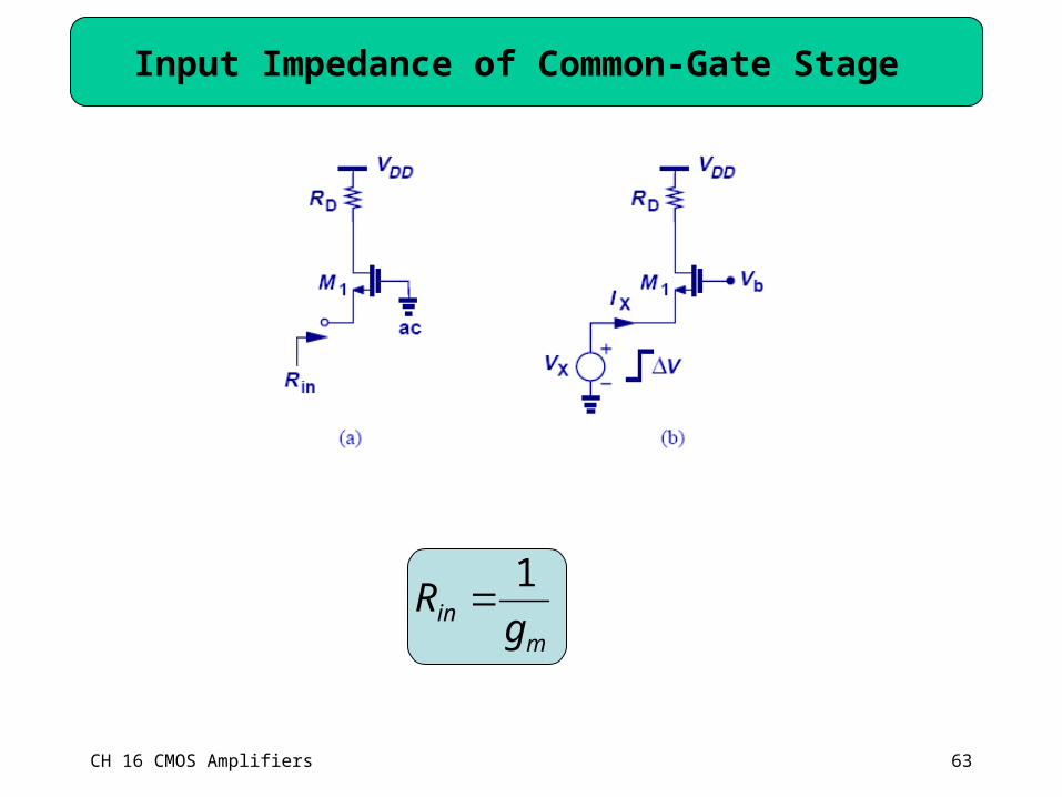
Input Impedance of Common-Gate Stage
63CH 16 CMOS Amplifiers
min g
R1

The Use of Low Input Impedance
64CH 16 CMOS Amplifiers
The low input impedance of a common-gate stage can be used to impedance match a 50-Ω transmission line.

Output Impedance of Common-Gate Stage
65CH 16 CMOS Amplifiers
DOout RrR ||

Example: Alternate Av Expression of CG Stage
66CH 16 CMOS Amplifiers
in
outv R
RA

CG Stage in the Presence of Finite Source Resistance
67CH 16 CMOS Amplifiers
Sm
D
in
out
Rg
R
v
v
1

Output Impedance of a General CG Stage
68CH 16 CMOS Amplifiers
SOSmDout RrRgRR 1||

CG and CS Stages Output Impedance Comparison
69CH 16 CMOS Amplifiers
SOSmDoutCSoutCG RrRgRRR 1||
Since when calculating the output impedance, the input voltage source of the CG stage is grounded, the result will be identical to that of a CS stage if the same assumptions are made for both circuits.

Example: AV and Rout
70CH 16 CMOS Amplifiers
Smm
Dm
in
out
Rgg
Rg
v
v
21
1
1
λ = 0
DOSm
Omout RrRg
rgR ||||1
12
11
λ > 0

Example: CG Stage Lacking Bias Current
71CH 16 CMOS Amplifiers
Although the capacitor C1 isolates the DC content of the signal source, it also blocks the bias current of M1, hence turning it OFF.

Example: CG Stage with Source Shorted to Ground
72CH 16 CMOS Amplifiers
Although there is now a path for bias current to flow to ground, the signal current also goes with it, hence producing no gain.

CG Stage with Proper Bias Circuitry
73CH 16 CMOS Amplifiers
R1 is used to provide a path for bias current to flow without directly shorting the source to ground.
However, it also lowers the input impedance of the circuit
1||1
Rg
Rm
in DmSm
v RgRRg
A
111
1

Input Current Flowing Paths
74CH 16 CMOS Amplifiers
To maximize the useful current i2, R1 needs to be much larger than 1/gm.
mgR
11
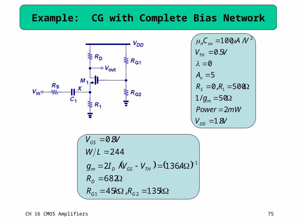
Example: CG with Complete Bias Network
75CH 16 CMOS Amplifiers
VV
mWPower
g
RR
A
VV
VAC
DD
m
S
v
TH
oxn
8.1
2
50/1
500,0
5
0
5.0
/100
1
2
kRkR
R
VVIg
LW
VV
GG
D
THGSDm
GS
135,45
682
4.136/2
244
8.0
21
1

Example: Min W/L
76CH 16 CMOS Amplifiers
VV
mWPower
g
RR
A
VV
VAC
DD
m
S
v
TH
oxn
8.1
2
50/1
500,0
5
0
5.0
/100
1
2
2
1
1
1
22
22
v
RDDoxn
D
RTHGSTHGSv
DD
THRGSDDDD
AVV
C
I
L
W
VVVVVA
V
VVVRIV

Source Follower
77CH 16 CMOS Amplifiers
Source follower sense the input at the gate and produces the output at the source.
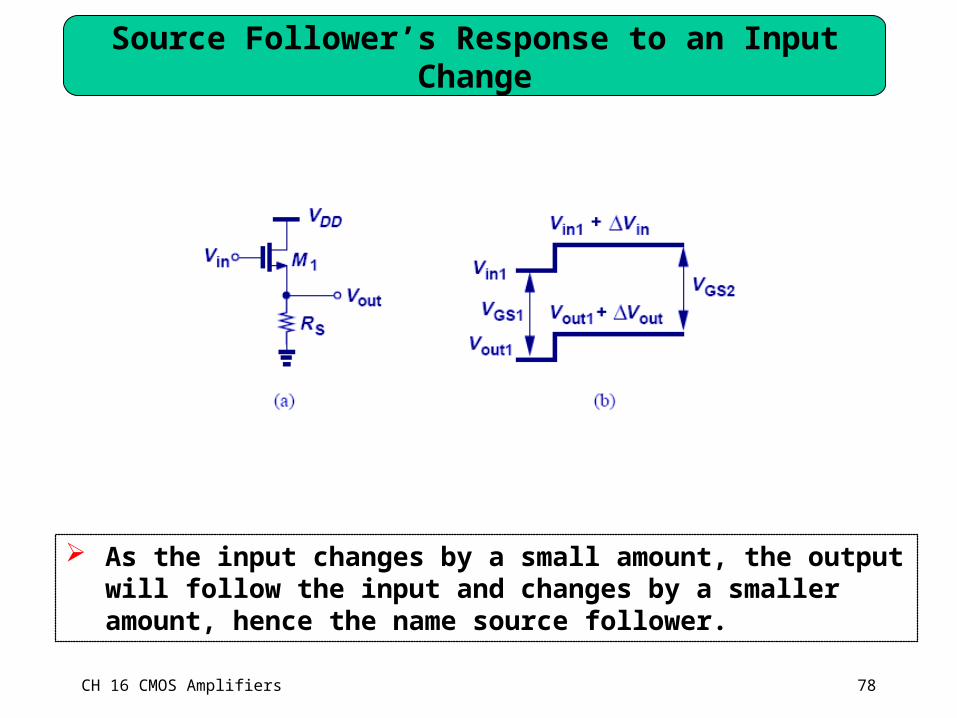
Source Follower’s Response to an Input Change
78CH 16 CMOS Amplifiers
As the input changes by a small amount, the output will follow the input and changes by a smaller amount, hence the name source follower.

Small-Signal Model and Voltage Gain for Source Follower
79CH 16 CMOS Amplifiers
mS
S
in
out
gR
R
v
v1

Example: Source Follower with Current Source
80CH 16 CMOS Amplifiers
AV
1vA

Source Follower Acting as a Voltage Divider
81CH 16 CMOS Amplifiers
mS
S
in
out
gR
R
v
v1

Complete Small-Signal Model with rO
82CH 16 CMOS Amplifiers
mSO
SO
in
out
gRr
Rr
v
v1
||
||

Example: Source Follower with a Real Current Source
83CH 16 CMOS Amplifiers
mOO
OOv
grr
rrA
1||
||
21
21

Example: Source Follower with a Real Current Source
84CH 16 CMOS Amplifiers
VV
VV
VAC
mWPower
A
R
DD
TH
oxn
v
S
8.1
0
5.0
/100
10
5.0
50
2
36050
1
5.01
LW
g
Rg
RA
m
Sm
Sv

Output Resistance of Source Follower
85CH 16 CMOS Amplifiers
SOm
out Rrg
R ||||1

Example: Source Follower with Biasing
86CH 16 CMOS Amplifiers
kR
VV
VV
VAC
A
mAI
G
DD
TH
oxn
v
D
50
8.1
0
5.0
/100
8.0
1
2
107
933.0
867
2
LW
VRIVV
RR
I
VVR
A
SDDDGS
S
SD
THGS
Sv

Source Follower with Current Source Biasing
87CH 16 CMOS Amplifiers
In IC technology, source follower is often biased by a current source to avoid the bias current’s dependence on the supply voltage.

Summary of MOS Amplifier Topologies
88CH 16 CMOS Amplifiers

Example: Common Source Stage I
89CH 16 CMOS Amplifiers
3213
3213
1
||||||1
||||||1
OOOm
out
OOOm
mv
rrrg
R
rrrg
gA

Example: Common Source Stage II
90CH 16 CMOS Amplifiers
331
2
||11
Omm
Ov
rgg
rA

Example: CS and CG Stages
91CH 16 CMOS Amplifiers
Sm
OvCG
OOSOmmvCS
Rg
rA
rrRrggA
1
2
11112
1
||1

Example: Composite Stage I
92CH 16 CMOS Amplifiers
21
11
mm
Dv
gg
RA

Example: Composite Stage II
93CH 16 CMOS Amplifiers
221
4332
12
2
221
||11
||||1
1||
1
||1
Omm
OOm
in
out
mO
m
Om
in
out
rgg
rrg
v
v
gr
g
rg
v
v

Chapter Summary
94CH 16 CMOS Amplifiers
The impedances looking into the gate, drain, and source of a MOS are equal to ∞, rO and 1/gm respectively (under proper conditions).
The transistor has to be properly biased before small-signal can be applied.
Resistive path between the supply rails establishes the gate bias voltage.
Only three amplifiers topologies are possible. CS stage provides moderate AV, high Rin and moderate Rout.
Source degeneration improves linearity but lower AV.
Source degeneration raises the Rout of CS stage considerably.
CG stage provides moderate AV, low Rin and moderate Rout.
AV for CS and CG stages are similar but for a sign.
Source follower provides AV less than 1, high Rin and low Rout, serving as a good voltage buffer.


![Wide-Bandga 16.Wide-BandgapII-VISemiconductors ... · molecular-beam epitaxy (MBE) [16.3], metalorganic molecular-beam epitaxy (MOMBE) [16.4] and atomic-layer epitaxy (ALE) [16.5].](https://static.fdocuments.net/doc/165x107/5e1f371b74bffa7fb71fc624/wide-bandga-16wide-bandgapii-visemiconductors-molecular-beam-epitaxy-mbe.jpg)