Chapter 14 Introduction to Microprocessors. 2 Microcomputer A self-contained computer system that...
68
Chapter 14 Introduction to Microprocessors
-
Upload
britney-lee -
Category
Documents
-
view
238 -
download
0
Transcript of Chapter 14 Introduction to Microprocessors. 2 Microcomputer A self-contained computer system that...

Chapter 14
Introduction to Microprocessors

2
Microcomputer
• A self-contained computer system that consists of CPU (central processing unit), memory (RAM and ROM) and peripheral devices.
• A peripheral device acts as the interface between the computer and the external world.

3
Microcomputer

4
Microprocessor
• The part of a computer that generates control signals for the other components.
• Performs arithmetic and logic functions.

5
Busses – 1
• Busses are generally parallel groups of conductors that carry signals among the components of a microcomputer.
• The three types of busses are address, data, and control.
6
Busses – 2
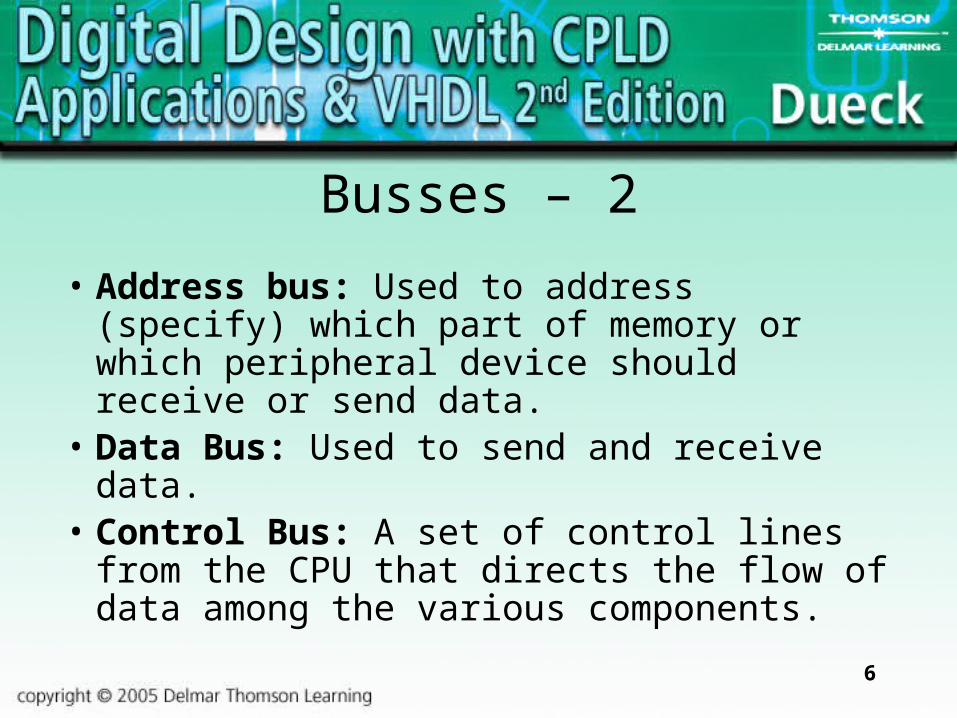
• Address bus: Used to address (specify) which part of memory or which peripheral device should receive or send data.
• Data Bus: Used to send and receive data.• Control Bus: A set of control lines from
the CPU that directs the flow of data among the various components.

7
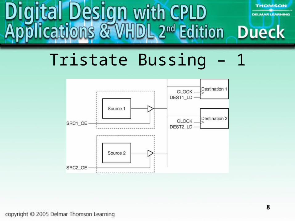
Tristate Bussing – 1
• Used to prevent more than one device from writing to the bus at a time.
• Avoids bus contention (conflicting signals on the bus).
• Tristate devices can be in one of three possible states: logic HIGH, LOW, or high impedance.
8
Tristate Bussing – 1

9
Tristate Bussing – 2
• In Figure 14.2, the source registers write data to the bus when the output enable lines SRC1_OE or SRC2_OE are HIGH.
• The destination registers accept data when a positive edge clock is applied to DEST1_LD or DEST2_LD when they are HIGH.

10
Tristate Bussing – 2

11
Synchronous Data Transfer
• In Figure 14.2, the data transfer is susceptible to errors due to propagation delay and asynchronous changes in data.
• Synchronous data transfer is much more stable.
• Synchronous data transfer synchronizes the source output with the system clock.

12
Synchronous Data Transfer

13
Synchronous Data Transfer

14
RISC8v1 MCU – 1
• See Figure 14.6 in textbook• RISC reduced instruction set computer.• 8-bit data bus. • 4-bit address bus.• Can be programmed into the FLEX10K.
device on the UP-2 board.

15
RISC8v1 MCU – 2
• Each block can be programmed in VHDL.
• Blocks are controlled by output enable (OE) and load signals (LD).
• Program instructions are stored in ROM.

16
RISC8v1 MCU Instruction Set
• LOAD – Transfers data from ROM to the accumulator.
• ADD – Transfers data from ROM to the memory data register (MDR), uses the ALU to add the data in the MDR.
• OUTPUT – Transfers data from the accumulator to the output.
• HALT – Stops the program.

17
RISC8v1 MCU Op Code – 1
• The 4 instructions correspond to a 4-bit code called an op code.
• Usually written in binary or HEX.• The op code is determined by the design
of the instruction decoder.• The op code may require an operand
(data that is operated on by the computer).

18
RISC8v1 MCU Op Code – 2
Instruction HEX Value
ADD 1
LOAD 8
OUTPUT 9
HALT F

19
RISC8v1 Control Unit
• The control unit has three functions:– Fetch an instruction from memory– Decode the instruction to determine which
operation is to be performed– Execute the instruction

20
RISC8v1 MCU Sample Program
Address Data CommentC 8C Load contents of C1 1D Add contents of D2 90 Send accumulator contents to the output register3 F0 HALT
4-B Blank (00)
C 55 Data for LOAD instructionD 64 Data for ADD instruction
E-F Blank (00)

21
Fetch Cycle – 1• Fetch 1 – Transfers the content of the
program counter (PC) to the address bus (see Figure 14.7 in textbook).
• Fetch 2 – Transfers the PC address to the memory address register (see Figure 14.8 in textbook).
• Fetch 3 – Transfers the instruction from ROM to to the data bus (see Figure 14.9 in textbook).

22
Fetch Cycle – 2
• Fetch 4 – The op code/address pair transfers to the instruction register (see Figure 14.10 in textbook).
• Fetch 5 – Wait.

23
Fetch Cycle – 3

24
Execute Cycle LOAD – 1
• Load 1 – The instruction/operand address pair is divided into the op code and operand address (see Figure 14.13 in textbook).
• Load 2 – MAR loads the contents of the address bus, latching the ROM address of the operand for the LOAD instruction (see Figure 14.14 in textbook).

25
Execute Cycle LOAD – 2
• Load 3 – Data transfers from ROM to data bus (see Figure 14.15 in textbook).
• Load 4 – Data transfers from the data bus to the accumulator (see Figure 14.16 in textbook).

26
Execute Cycle LOAD – 3

27
Arithmetic Logic Unit (ALU) – 1
• Capable of performing four 8-bit arithmetic functions and four 8-bit bitwise logic functions.
• Functions selected by select inputs S2, S1, and S0.

28
Arithmetic Logic Unit (ALU) – 2
S[2..0] Function Operation000 Increment Acc + 1001 Add Acc + MDR010 Subtract Acc - MDR011 Decrement Acc - 1100 Comlement NOT Acc101 AND Acc AND MDR110 OR Acc OR MDR111 XOR Acc XOR MDR

29
VHDL Code ALU
• LIBRARY ieee;• USE ieee.std_logic_1164.ALL;• USE ieee.std_logic_signed.ALL;• USE ieee.std_logic_arith.ALL;

30
VHDL Code ALU Entity
ENTITY alu IS
PORT (
operand_a : IN STD_LOGIC_VECTOR ( 7 downto 0);
s : IN STD_LOGIC_VECTOR ( 2 downto 0);
memory_data : IN STD_LOGIC_VECTOR ( 7 downto 0);
alu_data : OUT STD_LOGIC_VECTOR ( 7 downto 0));
END alu;

31
VHDL Code ALU Architecture – 1
ARCHITECTURE a OF alu IS
BEGIN
PROCESS (operand_a, memory_data, s)
BEGIN
CASE s IS
WHEN “000” =>
alu_data <= operand_a + 1; -- Increment A
WHEN “001” =>
alu_data <= operand_a + memory_data; -- Add
32
VHDL Code ALU Architecture – 2
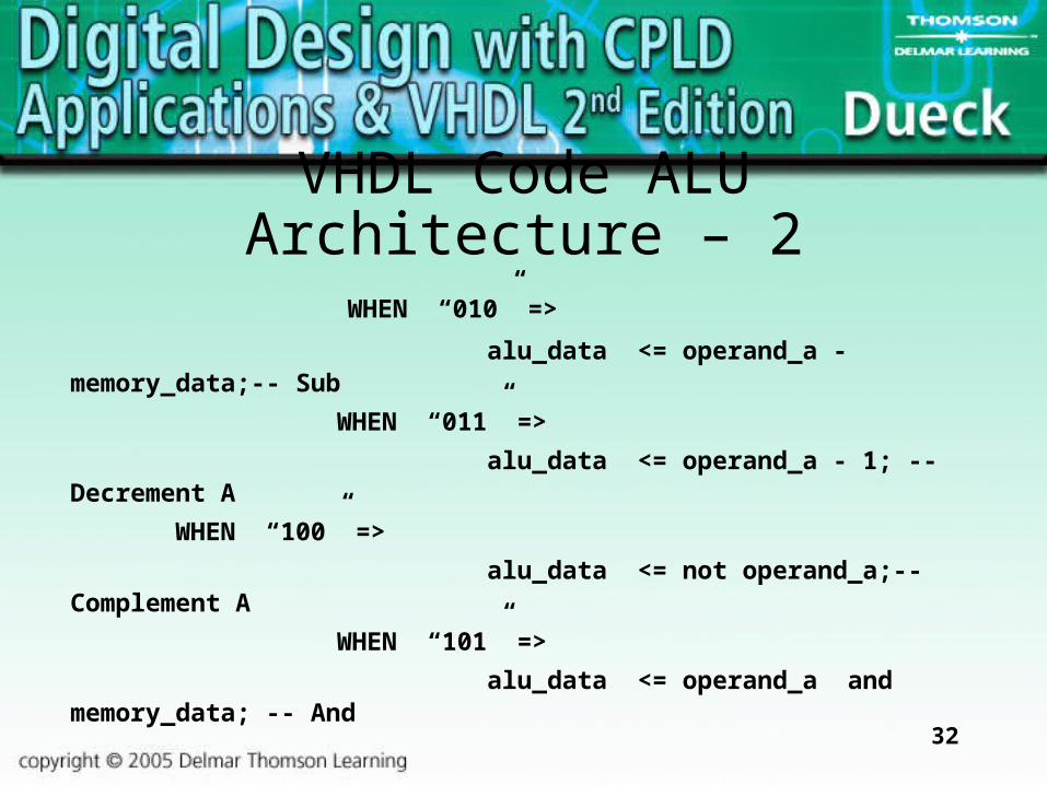
WHEN “010” =>
alu_data <= operand_a - memory_data;-- Sub
WHEN “011” =>
alu_data <= operand_a - 1; -- Decrement A
WHEN “100” =>
alu_data <= not operand_a;-- Complement A
WHEN “101” =>
alu_data <= operand_a and memory_data; -- And

33
VHDL Code ALU Architecture – 3
WHEN “110” =>
alu_data <= operand_a or memory_data;-- Or
WHEN “111” =>
alu_data <= operand_a xor memory_data;-- Xor
WHEN others =>
alu_data <= (others => ‘0’);

34
Execute Cycle ADD – 1• First three cycles the same as for LOAD
(see Figures 14.18, 14.19 and 14.20 in textbook), except the s inputs are set to 001.
• Add 4 – Transfers data from the data bus to the MDR (see Figure 14.21 in textbook).
• Add 5 – The ALU adds the accumulator contents to the MDR contents.

35
Execute Cycle ADD – 2
• Add 6 – Accumulator transfers the final result from the data bus to the accumulator (see Figure 14.23 in textbook).
• Figure 14.24 in textbook – ADD fetch cycle timing diagram.
• Figure 14.25 in textbook – ADD execute cycle timing diagram.

36
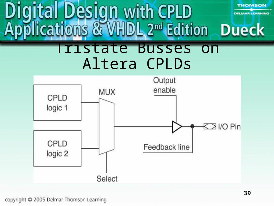
Tristate Busses on Altera CPLDs
• Tristate driver connects to I/O pin only.• Either connect the I/O pins external to
the CPLD or multiplex internal logic to a single tristate pin.

37
Tristate Busses on Altera CPLDs

38
Tristate Busses on Altera CPLDs
39
Tristate Busses on Altera CPLDs

40
Tristate Addressing RISC8v1
• Addressing system consists of:– The program counter– Instruction register– Memory address register– Synchronous tristate address MUX

41
Tristate Addressing RISC8v1

42
Tristate Addressing RISC8v1

43
Quartus II Block Diagram File – 1
• Uses blocks instead of graphics symbols.
• A block is a design unit that represents a subunit such as a bdf or VHDL file.
• Inputs and outputs are indicated by a table embedded in the block.

44
Quartus II Block Diagram File – 2
• Blocks can be connected by node and bus lines or can be connected by conduit lines.
• A conduit line connects signals going between blocks by matching names on the connected block I/O list.
• Conduit lines are indicated by a “hollow line” on the block diagram.
45
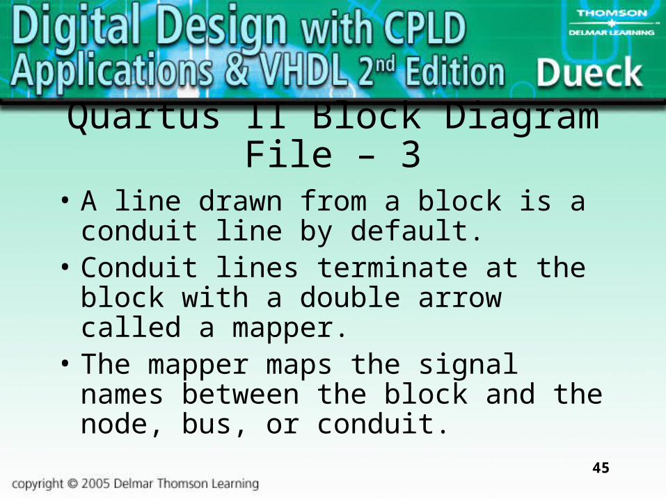
Quartus II Block Diagram File – 3
• A line drawn from a block is a conduit line by default.
• Conduit lines terminate at the block with a double arrow called a mapper.
• The mapper maps the signal names between the block and the node, bus, or conduit.

46
Implementing the RISC8v1 – 1
• Referring to Figure 14.41 in the textbook, the RISC8v1 is comprised of the following (VHDL) blocks:– instruction_register– program_counter– memory_address_register– address_mux

47
Implementing the RISC8v1 – 2
– rom– accumulator– memory_data_register– data_mux– output_register– controller_v1

48
The IR Block
• Data latched from the data bus on a positive clock edge when ir_ld is HIGH.
• Latched data is split into an instruction part and a operand address part.

49
The Program Counter (PC) Block
• Output connects to the address bus via the tristate address bus MUX.
• 4-bit binary counter with count enable.• Increments once every Fetch/Execute
cycle.

50
PC – VHDL Code
-- Program Counter
-- 4 bit counter with active-LOW asynchronous reset
-- Increments when PC_INC is HIGH
LIBRARY ieee;
USE ieee.std_logic_1164.ALL;
USE ieee.std_logic_unsigned.ALL;
51
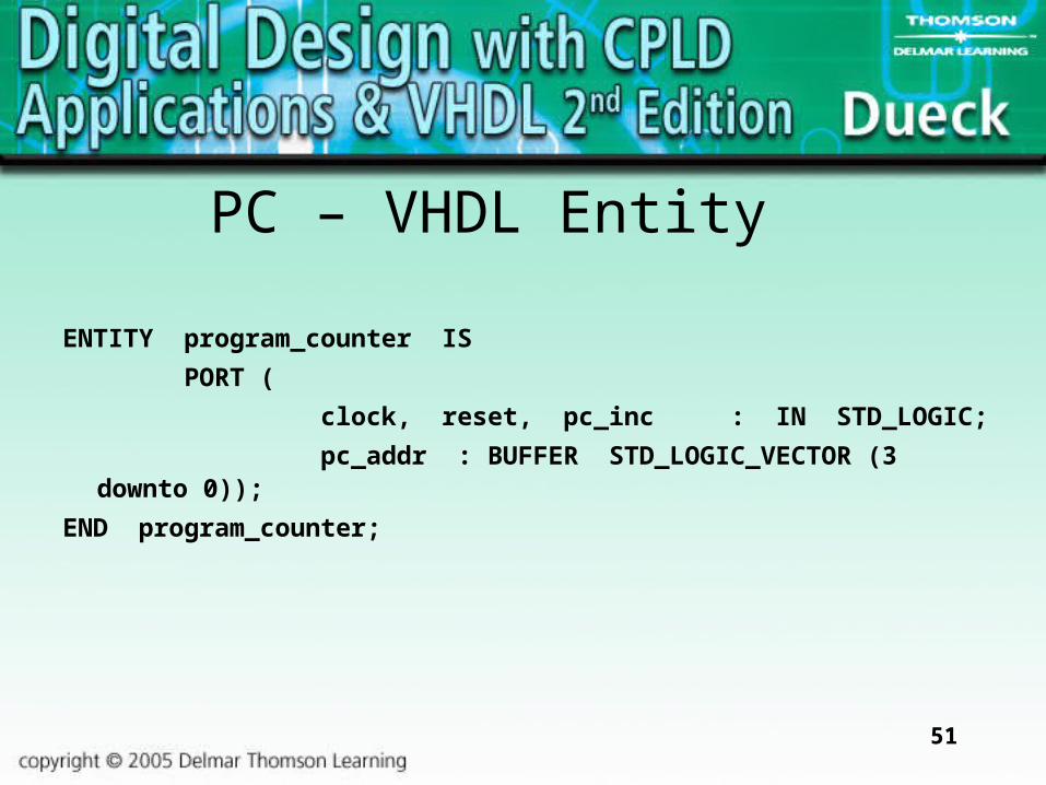
PC – VHDL Entity
ENTITY program_counter IS
PORT (
clock, reset, pc_inc : IN STD_LOGIC;
pc_addr : BUFFER STD_LOGIC_VECTOR (3 downto 0));
END program_counter;

52
PC – VHDL Architecture ARCHITECTURE pc OF program_counter ISBEGIN PROCESS (clock, reset) BEGIN IF (reset = ‘0’) THEN pc_addr <= (others => ‘0’); ELSEIF (clock ‘EVENT and clock = ‘1’) THEN IF (pc_inc = ‘1’) THEN pc_addr <= pc_addr + 1; END IF; END IF; END PROCESS;END pc;

53
The MAR Block
• When enabled, data is latched from the address bus on the positive clock edge.
• Outputs directly connect to the ROM.

54
The Address MUX Block
• Uses a separate select input for each logic signal to be MUX’ed.
• Combined into an internal signal called controls.
• CASE statement used to select which logic input is to be switched to the MUX.
• Data applied asynchronously, latched synchronously to the address bus.

55
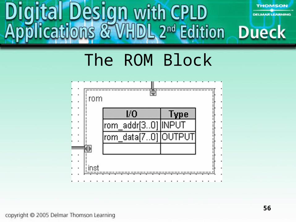
The ROM Block
• Program instructions and operands are stored in the LPM_ROM component, instantiated as a megafunction.
• The parameter LPM_File points to a Memory Initialization File (MIF).
• During compilation the ROM is loaded with the contents of MIF.
56
The ROM Block

57
The Accumulator Block
• Constructed from an 8-bit flip-flop with input and output enables.
• Data latched when acc_ld is HIGH.• Data directly applied to the 8-bit input port
of the ALU through operand_a[7..0].• Data synchronously sent to data bus
when acc_oe is HIGH.

58
The Accumulator Block

59
The MDR Block
• Has no output to the system data bus.• Data loaded synchronously when
mdr_ld is HIGH.• Port memory_data [7..0] connects
directly to the ALU without any enable.

60
The MDR Block

61
The Data Bus MUX Block
• Necessary to implement a tristate bus on an Altera CPLD.
• Combines output data from the ROM, ALU, or accumulator, selects one of these lines to go to the 8-bit data bus.
• Bidirectional pin acts as a data bus allowing input and output signals to go to and from the MUX.

62
The Data Bus MUX Block

63
The Output Register Block
• An 8-bit flip-flop that is synchronously loaded when or_ld is HIGH.

64
The Output Register Block

65
The Controller Block – 1
• Interprets the CPU instructions and generates the control signals for all registers to correctly execute the program functions.
• Implemented as a VHDL-based state machine.

66
The Controller Block – 2
• The state machine:– Defines the state type and lists all states in
the machine.– Uses two CASE statements to define the
actual progress of states.

67
The Controller Block – 3
• Uses concurrent signal assignment statements to map the output ports to a 16-bit internal signal control_word.
• Uses a select signal assignment statement to decode the states of the state machine and generate the required control signals by assigned them to control_word.

68
The Controller Block – 3