
CHAPTER 14€¦ · · 2010-02-04CHAPTER 14 Exercises E14.1 (a) A A A R v i = B B BR v i = B B A A...
46
CHAPTER 14 Exercises E14.1 (a) A A A R v i = B B B R v i = B B A A B A F R v R v i i i + = + = + − = − = B B A A F F F o R v R v R i R v (b) For the v A source, A A A A R i v R = = in . (c) Similarly . in B B R R = (d) In part (a) we found that the output voltage is independent of the load resistance. Therefore, the output resistance is zero. E14.2 (a) mA 1 1 1 = = R v i in mA 1 1 2 = = i i V 10 2 2 − = − = i R v o 460
Transcript of CHAPTER 14€¦ · · 2010-02-04CHAPTER 14 Exercises E14.1 (a) A A A R v i = B B BR v i = B B A A...

CHAPTER 14
Exercises
E14.1
(a)
A
AA R
vi = B
BB R
vi = B
B
A
ABAF R
vRviii +=+=
+−=−=
B
B
A
AFFFo R
vRvRiRv
(b) For the vA source, AA
AA R
ivR ==in .
(c) Similarly .in BB RR = (d) In part (a) we found that the output voltage is independent of the load resistance. Therefore, the output resistance is zero.
E14.2 (a)
mA 1
11 ==
Rvi in mA 112 == ii V 1022 −=−= iRvo
460

mA 10−==L
oo R
vi mA 112 −=−= iii ox
(b)
mA 5
11 ==
Rvi in mA 512 == ii V 5223 == iRv
mA 53
33 ==
Rvi mA 10324 =+= iii V 152244 −=−−= iRiRvo
E14.3
Direct application of circuit laws gives
1
11 R
vi = , 12 ii = , and 223 iRv −= .
From the previous three equations, we obtain 12v13 v1
2
RRv −=−= . Then
applying circuit laws gives 3
33 R
vi = , 4
24 R
vi = , 435 iii += , and .55iRvo −=
461
These equations yield 24
53
3
5 vRRv
RRvo −−=
,2 1
. Then substituting values and
using the fact that 3 vv −= we find .24 21 vvvo −=
vs 1in −= ii
in3 vvi s =+ 1in
+==vvA o
v
1 RR =
Rv
Rin
2
in =
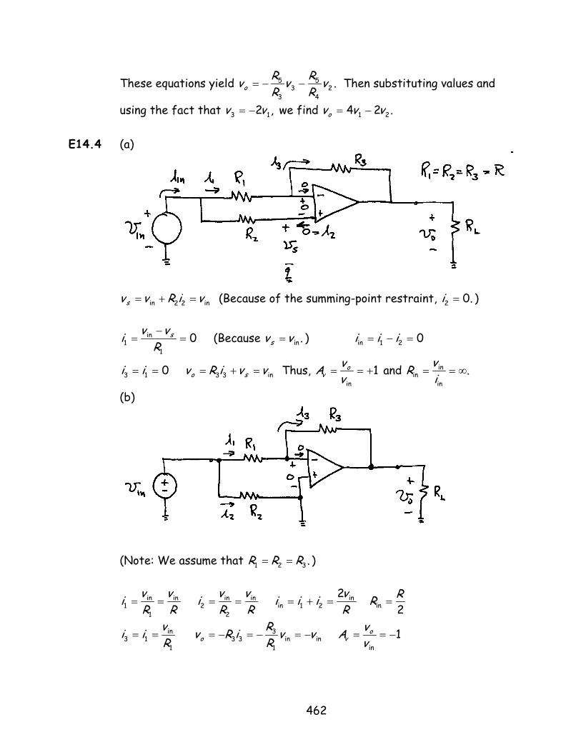
E14.4 (a)
in22in viRvvs =+= (Because of the summing-point restraint, .02 =i )
01
in1 =
−=
Rvvi s (Because .inv= ) 02 =i
013 == ii 3Rvo = Thus, and .in
inin ∞==
ivR
(b)
(Note: We assume that .32 R= )
Rv
Rvi in
1
in1 ==
Rviii in
21in2
=+= 2inRR = vi2 =
1
in13 R
vii == inin1
333 vv
RRiRvo −=−=−= 1
in
−==vvA o
v
462
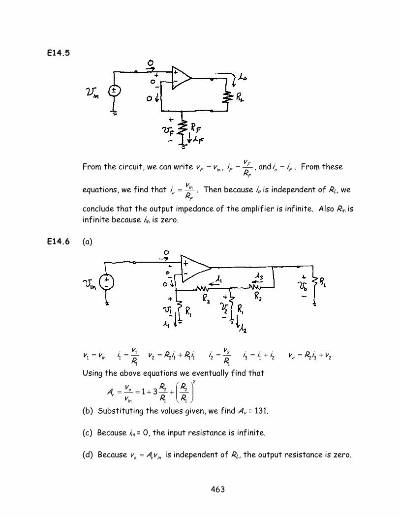
E14.5
From the circuit, we can write invvF = ,
F
FF R
vi = , and Fo ii = . From these
equations, we find that F
o Rvi in= . Then because io is independent of RL, we
conclude that the output impedance of the amplifier is infinite. Also Rin is infinite because iin is zero.
E14.6 (a)
in1 vv = 1
11 R
vi = 11122 iRiRv += 1
22 R
vi = 213 iii += 232 viRvo +=
Using the above equations we eventually find that
2
1
2
1
2
in
31
++=
RR
RR
vvo=Av
(b) Substituting the values given, we find Av = 131. (c) Because iin = 0, the input resistance is infinite. (d) Because invo vAv = is independent of RL, the output resistance is zero.
463

E14.7 We have 1
2
RRRA
svs +
−= from which we conclude that
20.1099.09.490
01.1499min1min
max2max −=
×+×
−=+
−=RR
RAs
vs
706.901.19.49500.0
99.0499max1max
min2min −=
×+×
−=+
−=RR
RAs
vs
E14.8
Applying basic circuit principles, we obtain:
11
1
sRR1vi = + 12iRvA −=
A
AA R
vi =
2
2
sBB RR
vi+
= BAf iii += ffo iRv −=
From these equations, we eventually find
22
111
2 vRR
RvRR
RRRv
Bs
f
A
f
s +−
+o =
E14.9 Many correct answers exist. A good solution is the circuit of Figure 14.11
in the book with .19 12 RR ≅
11
We could use standard 1%-tolerance resistors with nominal values of =R kΩ and 1.192 =R kΩ.
E14.10 Many correct answers exist. A good solution is the circuit of Figure 14.18 in the book with sRR 201 ≥ and ).(25 12 sRRR +≅ We could use
464

standard 1%-tolerance resistors with nominal values of 201 =R kΩ and 5152 =R kΩ.
=1R
2 =R1=AR.1=fR
0
==CL
t
Af
2SR
=πFPf
omfVπ2
=Vom
E14.11 Many correct selections of component values can be found that meet the
desired specifications. One possibility is the circuit of Figure 14.19 with:
a 453-kΩ fixed resistor in series with a 100-kΩ trimmer (nominal design value is 500 kΩ) RB is the same as R1
499 kΩ 5. MΩ 5 MΩ
After constructing the circuit we could adjust the trimmers to achieve the desired gains.
E14.12 kHz 40100
40105
0
0 =×
=CL
BOLOLBCL A
fAf The corresponding Bode plot is
shown in Figure 14.22 in the book.
E14.13 (a) kHz 9.198)4(2
105 6
=×
=πomV
(b) The input frequency is less than fFP and the current limit of the op amp is not exceeded, so the maximum output amplitude is 4 V. (c) With a load of 100 Ω the current limit is reached when the output amplitude is 10 mA × 100 Ω = 1 V. Thus the maximum output amplitude without clipping is 1 V. (d) In deriving the full-power bandwidth we obtained the equation: = SR Solving for Vom and substituting values, we have
7958.0102105
2 6
6
=×
=ππf
SR V
With this peak voltage and RL = 1 kΩ, the current limit is not exceeded.
465

(e) Because the output, assuming an ideal op amp, has a rate of change exceeding the slew-rate limit, the op amp cannot follow the ideal output, which is
)102sin(10)( 6ttvo π= . Instead, the output changes at the slew-rate limit and the output waveform eventually becomes a triangular waveform with a peak-to-peak amplitude of SR × (T/2) = 2.5 V.
E14.14 (a)
Applying basic circuit laws, we have
1
inin R
vi = and in2iRvo −= . These
equations yield 1
2
in RR
vvA o
v −== .
(b)
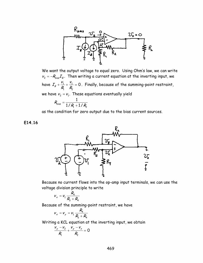
466

Applying basic circuit principles, algebra, and the summing-point restraint, we have
Bbiasyx IRvv −== BBbiasx I
RRRI
RR
Rvi
21
2
111 +
−=−==
BB IRR
RIR
R21
1
21
2
+=
+B R
iIi 12 1
−=+=
021
1222 =−
+=+= BbiasBxo IRI
RRRRviRv
(c)
The drop across Rbias is zero because the current through it is zero. For the source Voff the circuit acts as a noninverting amplifier with a gain
.1111
2 =+=RRAv
33off ±
Therefore, the extreme output voltages are given by
mV. == VAv vo (d)
Applying basic circuit principles, algebra, and the summing-point restraint, we have
467

2offIRvv biasyx ==
22off
21
2off
111
IRR
RIR
RRvi biasx
+===
22
21
2off
21
21off
21
21
off2
IRRRRI
RRRiIi
++
=
+
+=+=
offbiasxo IRIRIRRRRRviRv 2
offoff
21
21222 22
2=+
++
=+=
Thus the extreme values of ov caused by Ioff are mV. 4Ioff, ±=oV
(e) The cumulative effect of the offset voltage and offset current is that Vo ranges from -37 to +37 mV.
E14.15 (a)
Because of the summing-point constraint, no current flows through Rbias so the voltage across it is zero. Because the currents through R1 and R2 are the same, we use the voltage division principle to write
21
11 RR
Rvv o +=
Then using KVL we have 1in 0 vv +=
These equations yield
1
2
in
1RR
vvA o
v +==
Assuming an ideal op amp, the resistor Rbias does not affect the gain since
the voltage across it it zero. (b) The circuit with the signal set to zero and including the bias current
sources is shown.
468
We want the output voltage to equal zero. Using Ohm’s law, we can write
BIRv bias2 −= . Then writing a current equation at the inverting input, we
have 02
1 =+R1
1+v
RvIB
2
. Finally, because of the summing-point restraint,
we have .1vv = These equations eventually yield
21
bias /1/11
RR +=R
as the condition for zero output due to the bias current sources. E14.16
Because no current flows into the op-amp input terminals, we can use the voltage division principle to write
43
41 RR
Rvvx +=
Because of the summing-point restraint, we have
43
41 RR
Rvvv yx +==
Writing a KCL equation at the inverting input, we obtain
021
2 =−
+−
Rvv
Rvv oyy
469

Substituting for vy and solving for the output voltage, we obtain
1
22
1
21
43
41 R
RvR
RRRR
Rvvo −+
+=
If we have ,// 1234 RRRR = the equation for the output voltage reduces to
( )211
2 vvRRvo −=
E14.17 (a) ∫∫ −=−=tt
o dttvdttvRC
tv0
in0
in )(1000)(1)(
= ∫ −=−t
tdt0
500051000 for ms 10 ≤≤t
= for 1tdtdt 5000105-51000ms 1
0
t
ms 1
+−=
+− ∫ ∫ ms 3ms ≤≤t
and so forth. A plot of vo(t) versus t is shown in Figure 14.37 in the book. (b) A peak-to-peak amplitude of 2 V implies a peak amplitude of 1 V. The
first (negative) peak amplitude occurs at .ms 1 =t Thus we can write
34
ms 1
04
ms 1
0in 105
1015
10111 −××−=−=−=− ∫∫ C
dtC
dtvRC
which yields 0= F. 5. µC E14.18 The circuit with the input source set to zero and including the bias
current sources is:
Because the voltage across R is zero, we have iC = IB, and we can write
470
CtdtI
Cdti
Cv
t
B
t
Co
9
00
1010011 −×=== ∫∫
(a) For C = 0.01 µF we have V. 10)( ttvo = (b) For C = 1 µF we have V. 1.0)( ttvo = Notice that larger capacitances lead to smaller output voltages.
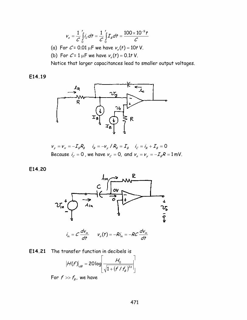
E14.19
BBxy RIvv −== BByR IRvi =−= / 0=+= BRC Iii Because 0=Ci , we have ,0=Cv and mV. 1=−== RIvv Byo
E14.20
dtdvCi in
in = dtdvRCRitvo
inin)( −=−=
E14.21 The transfer function in decibels is
( )
+=
nB
dB ffHfH
20
/1log20)(
For ,Bff >> we have
471
( )( ) )log(20log20log20
/log20)( 02
0 fnfnHff
HfH BnB
dB −+=
≅
This expression shows that the gain magnitude is reduced by 20n decibels for each decade increase in f.
E14.22 Three stages each like that of Figure 14.40 must be cascaded. From Table 14.1, we find that the gains of the stages should be 1.068, 1.586, and 2.483. Many combinations of component values will satisfy the requirements of the problem. A good choice for the capacitance value is 0.01 µF, for which we need .k 183.3)2/(1 Ω== BCfR π Also Ω= k 10fR is a good choice.
Problems
P14.1 An ideal operational amplifier has the following characteristics:
1. Infinite input impedance. 2. Infinite gain for the differential input signal. 3. Zero gain for the common-mode input signal. 4. Zero output impedance. 5. Infinite bandwidth.
P14.2 The probable functions of the five op amp terminals are the inverting input, the noninverting input, the output, and two power-supply terminals.
P14.3 The differential voltage is: 21 vvvid = −
and the common-mode voltage is: ( 212
1 )vvvicm +=
P14.4* )2000cos(21 tvvvid π=−= ( ) )120cos(20212
1 tvvvicm π=+= P14.5 The open-loop gain is the voltage gain of the op amp for the differential
input voltage with no feedback applied. Closed loop gain is the gain of circuit containing an op amp with feedback.
P14.6* The steps in analysis of an amplifier containing an ideal op amp are:
472
1. Verify that negative feedback is present. 2. Assume that the differential input voltage and the input currents are zero. 3. Apply circuit analysis principles including Kirchhoff’s and Ohm’s laws to write circuit equations. Then solve for the quantities of interest.
P14.7 According to the summing-point constraint, the output voltage of an op
amp assumes the value required to produce zero differential input voltage and zero current into the op-amp input terminals. This principle applies when negative feedback is present but not when positive feedback is present.
P14.8 The inverting amplifier configuration is shown in Figure 14.4 in the text. The voltage gain is given by 12 RRAv −= , the input impedance is equal to R1, and the output impedance is zero.
P14.9 This is an inverting amplifier having a voltage gain given by
312 −=−= RRAv . Thus, we have ( ) ( )[ ]tπtvo 2000cos23 ×−= Sketches of vin(t) and vo(t) are
473

P14.10* The circuit has negative feedback so we can employ the summing-point constraint. Then successive application of Ohm’s and Kirchhoff’s laws starting from the left-hand side of the circuit produces the results shown:
From these results we can use KVL to determine that in8vvo −= from which we have .8−=vA
P14.11 Because of the summing-point constraint, the voltages across the two resistors of value R are equal. Thus, the currents in the resistors of value R are equal as indicated:
Then applying KVL, we have RiiRvin += )2(2 and Rivo 15−= . Solving, we
find 3−==in
ov v
vA .
474

P14.12 Using the summing-point constraint, we have
)/exp(inTDsD nVvI
Rvi == and Do vv −=
Solving, we have
−=
sTo RI
vnVv inln
P14.13 Using the summing-point constraint, we have
)/exp( in TsD nVvIi = and Do Riv −= Thus, we have )/exp( in Tso nVvRIv −=
P14.14 Using the summing-point constraint, we have
3inDD Kv
Rvi == and Do vv −=
Solving, we have
3 in
KRvvo = −
P14.15 This circuit has positive feedback and the output can be either +10 V or
−10 V. Writing a current equation at the inverting input terminal of the op amp we have
020001000
2=
−+ ox−x vvv
Solving we find x ovv 3333.03333.1 +=
For 10=ov V, we have 333.4=xv V. On the other hand for 10−=ov V, we have 2−=xv V. Notice that for vx positive the output remains stuck at its positive extreme and for vx negative the output remains stuck at its negative extreme.
P14.16 This is an inverting amplifier with a voltage gain of −2. Thus, we have =xi 2 mA, 4−=Lv V, 4−=Li mA, and 6−=oi mA. In the circuit as shown,
there appears to be 6 mA flowing into the closed surface and no current flowing out. However, a real op amp also has power supply connections, and if the currents in these connections are taken into account, KCL is satisfied.
475

P14.17* The circuit diagram of the voltage follower is:
Assuming an ideal op amp, the voltage gain is unity, the input impedance is infinite, and the output impedance is zero.
P14.18* If the source has non-zero series impedance, loading (reduction in voltage) will occur when the load is connected directly to the source. On the other hand, the input impedance of the voltage follower is very high (ideally infinite) and loading does not occur. If the source impedance is very high compared to the load impedance, the voltage follower will deliver a much larger voltage to the load than direct connection.
P14.19 The noninverting amplifier configuration is shown in Figure 14.11 in the
text. Assuming an ideal op amp, the voltage gain is given by 121 RRAv += , the input impedance is infinite, and the output impedance
is zero. P14.20 (a) ( ) V 2mA 2k 1 −=×Ω−=ov
(b) V 1506 −=++−=ov
476

(c) No current flows through the 3-kΩ resistor. Thus V 3410 =+−=ov .
(d) 0=ov
(e)
V 325 =−=ov
P14.21* The circuit diagram is:
477

Writing a current equation at the noninverting input, we have
011 =−
+−
B
B
A
A
Rvv
Rvv (1)
Using the voltage-division principle we can write:
ovRR
Rv21
11 += (2)
Using Equation (2) to substitute for v1 in Equation (1) and rearranging, we obtain:
BA
ABBAo RR
RvRvR
RRv++
+=
1
21
P14.22 Analysis of the circuit using the summing-point constraint yields
++−= 4
2in4
2
101
10RvRvo
Substituting the expression given for vin yields
++π−−= 4
24
24
2
101)2000cos(
103
102 RtRRvo
Then setting the dc component to zero, we have
++−= 4
24
2
101
1020 RR
which yields R2 = 10 kΩ and then we have )2000cos(3 tvo π−= P14.23 (a)
21 00 vRiv o +++= R
vvio 21 −=
Since io is independent of the load, the output impedance is infinite.
478
(b) The circuit diagram is:
Writing KVL around loop #1, we have ininin RiRiv ++= 0 Writing KVL around loop #2, we have 0=++ inofin RiiRRi Algebra produces fino Rvi −= . Since io is independent of the load, the
output impedance is infinite. P14.24*
(a) info iRv −= (b) Since vo is independent of RL, the output behaves as a perfect voltage source, and the output impedance is zero. (c) The input voltage is zero because of the summing-point constraint, and the input impedance is zero. (d) This is an ideal transresistance amplifier.
479

P14.25 (a) Using the summing-point constraint, KCL, KVL, and Ohm's law, we find the currents:
Then, we find ino Riv 3= (b) Since vo is independent of RL, the output behaves as a perfect voltage source, and the output impedance is zero. (c) The input voltage is zero because of the summing-point constraint, and the input impedance is zero. (d) This is an ideal transresistance amplifier.
P14.26 (a) Using the current-division prinicple, we find the currents as shown:
Then, KVL around the input loop gives )3/( oin iRv = , which yields
Rvi ino /3= . (b) Since io is independent of RL, the output behaves as a perfect current source, and the output impedance is infinite. (c) The input current is zero because of the summing-point constraint, and the input impedance is infinite. (d) This is an ideal transconductance amplifier.
480
P14.27 (a) This is an inverting amplifier having 12 RRAv −= and 1RRin = . The
input power is 1
22
Rv
RvP s
in
sin ==
The output power is L
oo R
vP2
=
The power gain is LL
vs
Lo
in
o
RRR
RRA
RvRv
PPG
1
2212
12
2
====
(b) This is a noninverting amplifier having 0=ini . Therefore 0=inP , and
∞=G . Thus, the noninverting amplifier has the larger power gain.
P14.28* (a) This circuit has negative feedback. Assuming an ideal op amp, we have ( ) ( )tvtv ino −= .
(b) This circuit has positive feedback. Therefore, the summing-point
constraint does not apply.
From the circuit, we can write
0=−
+−
Rvv
Rvv oidinid
Solving for vid, we have
2
inoid
vvv +=
If vid > 0, then vo = +5. On the other hand, if vid < 0, then vo = -5.
481
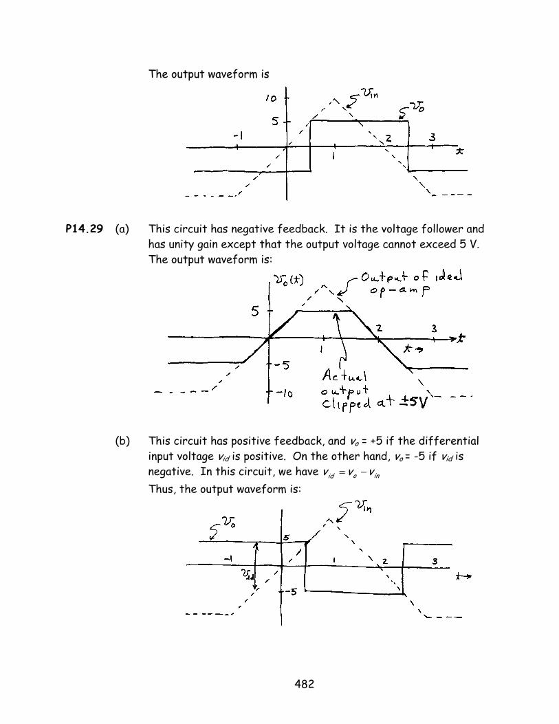
The output waveform is
P14.29 (a) This circuit has negative feedback. It is the voltage follower and has unity gain except that the output voltage cannot exceed 5 V. The output waveform is:
(b) This circuit has positive feedback, and vo = +5 if the differential
input voltage vid is positive. On the other hand, vo = -5 if vid is negative. In this circuit, we have inoid vvv −= Thus, the output waveform is:
482

P14.30 The inverting amplifier is shown in Figure 14.4 in the text and the voltage gain is 12 RRAv −= . Thus to achieve a voltage gain magnitude of 2, we would select the nominal values such that nom1nom2 2RR = . However for 5%-tolerance resistors, we have nom1max1nom1min1 05.1 95.0 RRRR ==
nom2max2nom2min2 05.1 95.0 RRRR == Thus we have
81.105.195.0
nom1
nom2
max1
min2 −=−=−=RminR
RRAv
21.295.005.1
nom1
nom2
min1
max2 −=−=−=RmaxR
RRAv
Thus Av= 2 plus 10.5% minus 9.5%. P14.31 The noninverting amplifier is shown in Figure 14.11 in the text, and the
voltage gain is 121 RRAv += . Thus to achieve a voltage gain magnitude of 2, we would select the nominal values such that nom1nom2 RR = . However for 5%-tolerance resistors, we have nom1max1nom1min1 05.1 95.0 RRRR == nom2max2nom2min2 05.1 95.0 RRRR == Thus we have
905.105.195.011
nom1
nom2
max1
min2min =+=+=
RR
RRAv
105.295.005.111
nom1
nom2
min1
max2max =+=+=
RR
RRAv
Thus Av= 2 ± 5%.
483

P14.32* The circuit diagram is:
ino iRRi
+−=
2
11
Because of the summing-point constraint, we have vin = 0. Thus, Rin = 0. Because the output current is independent of RL, the output impedance is infinite. In other words looking back from the load terminals, the circuit behaves like an ideal current source.
P14.33
By the voltage-division principle, we have
( ) ininx TvvRTRT
RTv =−+
=1
Then, we can write
( )R
TvR
vvi inxinx
−=
−=
1
xxo vRiv +−= ( ) inin TvTv +−−= 1 ( )12 −= Tvin
484

Thus, as T varies from 0 to unity, the circuit gain varies from -1 through to 0 to +1.
P14.34
From the circuit we can write: 31 vvo =
R
vii o134 ==
Thus we have 134 ovvv == 1432 2 oo vvvv =+=
044
21 =++R
vR
vi ooin
Rvi in
in =
044
21 =++R
vR
vRv ooin
3411 −==
in
o
vvA
38221
122 −==== A
vv
vvA
in
o
in
o
P14.35 Very small resistances lead to excessively large currents, possibly
exceeding the capability of the op amp, creating excessive heat or overloading the power supply.
485

Very large resistances lead to instability due to leakage currents over
the surface of the resistors and circuit board. Stray pickup of undesired signals is also a problem in high-impedance circuits.
P14.36* To achieve high input impedance and an inverting amplifier, we cascade a
noninverting stage with an inverting stage:
The overall gain is:
3
4
1
21
RR
RRRAv ×
+−=
Many combinations of resistance values will achieve the given specifications. For example:
0 and 21 =∞= RR . (Then the first stage becomes a voltage follower.) This is a particularly good choice because fewer resistors affect the overall gain, resulting in small overall gain variations. R4 = 100 kΩ, 5% tolerance. R3 = 10 kΩ, 5% tolerance.
P14.37* A solution is:
486
P14.38 Use the inverting amplifier configuration:
Pick R2nom = 10R1nom to achieve the desired gain magnitude.
Pick R1nom > 10 kΩ to achieve input impedance greater than 10 kΩ. Pick R1nom and R2nom < 10 MΩ because higher values are impractical. Many combinations of values will meet the specifications. For example: (a) Use 5% tolerance resistors. R1 = 100 kΩ and R2 = 1 MΩ. (b) Use 1% tolerance resistors. R1 = 100 kΩ and R2 = 1 MΩ.
(c) R2 =1 MΩ 1% tolerance. R1 = 95.3 kΩ 1% tolerance fixed resistor in series with a 10-kΩ adjustable resistor. After constructing the circuit, adjust to achieve the desired gain magnitude.
P14.39 We use a noninverting amplifier and place a resistor in parallel with the
input terminals to achieve the desired input impedance.
R1 = 1 kΩ, 1% tolerance. Many combinations of values for R2 and R3 will meet the given
specifications. For example: R2 = 1 kΩ, 1% tolerance. R3 = 9.09 kΩ, 1% tolerance. (These values result in a nominal gain of 10.09, which is within the
specified range.)
487

P14.40 Here are two answers:
Many other correct answers exist. P14.41* One possibility is to place unity-gain voltage follower circuits between
the sources and the input terminals of the circuits designed for Problem P14.40. A better answer (because it requires fewer op amps) is:
All resistors are 1% tolerance. ±
P14.42 To avoid excessive gain variations because of changes in the source
resistances, we need to have input resistances that are much greater than the source resistances. Many correct answers exist. Here is one possibility:
488

The fixed resistors should be specified to have a tolerance of ± 1% because they are more stable in value than 5% tolerance resistors. The adjustment procedure is:
1. Set v1 = 0 and v2 = + 1 V. Then, adjust the 2-kΩ potentiometer to obtain vo = 3 V.
2. Set v1 = 1 V and v2 = 0. Then, adjust the 1-kΩ potentiometer to obtain vo = -10.
P14.43 To avoid excessive variations in sovs vvA = because of changes in Rs, we
need to have sin RR >> . Rin =100 kΩ is sufficiently large. Thus, a suitable circuit is
R1 and R2 should be 1% tolerance resistors.
P14.44 Imperfections of real op amps in their linear range of operation include: 1. Finite input impedance. 2. Nonzero output impedance. 3. Finite dc open-loop gain. 4. Finite open-loop bandwidth.
489

P14.45* Equation 14.34 states: BOLOLBCLCLt fAfAf 00 == Thus, for A0CL = 10, we have
MHz 5.110MHz 15
0
===CL
tBCL A
ff
For A0CL = 100, we have fBCL = 150 kHz
P14.46 Equation 14.23 gives the open-loop gain as a function of frequency:
( ) ( ) ( )5110200
1
30
fjffjAfA
BOL
OLOL +
×=
+=
For f = 100 Hz, we have
( ) ( )5100110200100
3
jAOL +
×=
( )( )
99871
1002
0 =+
=BOL
OLOL
ffAA
Similarly, we have ( ) 10001000 =OLA ( ) 1106 =OLA
P14.47 (a)
From the circuit, we can write: ( )sinOLsosins iRAiRiRv ++= ( )sinOLsoo iRAiRv += Dividing the respective sides of the previous equations yields:
inOLoin
inOLo
s
ovo RARR
RARvvA
+++
==
Substituting values, we obtain:
656
65
10102510101025×++
×+=voA
490

= (compared to unity for an ideal op amp) 99999.0
(b) inOLoins
sin RARR
ivZ ++==
656 10102510 ×++= (compared to ∞ for an ideal op amp) Ω= 1011
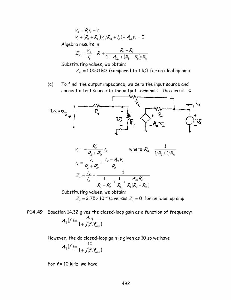
(c) The circuit for determining the output impedance is:
xi vv −=
o
iOLx
in
xx R
vAvRvi −
+=
o
OL
in
x
xo
RA
RivZ
++
== 111
Ω×= − 105.2 4oZ (versus Zo = 0 for an ideal op amp)
P14.48 (a) From the circuit (shown in Figure P14.48 in the text), we can write:
021
=++
++
in
iiois
Rv
Rvv
Rvv
02
=−
++
o
iOLoio
RvAv
Rvv
Algebra results in:
−+
+++
−==
oOL
o
in
s
ovo
RRARRR
RRRR
RvvA
2
222
211
2
1111
Substituting values, we obtain: 9989.9−=voA (compared to -10 for an ideal op amp) (b) From the circuit, we can write:
491
isis viRv −= ( )( ) 02 =++++ iOLsinioi vAiRvRRv Algebra results in
( ) inoOL
o
s
sin RRRA
RRRivZ
++++
+==2
21 1
Substituting values, we obtain: Ω= k 0001.1inZ (compared to 1 kΩ for an ideal op amp (c) To find the output impedance, we zero the input source and
connect a test source to the output terminals. The circuit is:
xin
ini v
RRRv
′+′
−=2
where inRR 11
11 +
=inR ′
o
iOLx
in
xx R
vAvRR
vi −+
′+=
2
( )ino
inOL
oin
x
xo
RRRRA
RRRivZ
′+′
++′+
==
22
111
Substituting values, we obtain: 0 versus 1075.2 3 =Ω×= −
oo ZZ for an ideal op amp P14.49 Equation 14.32 gives the closed-loop gain as a function of frequency:
( ) ( )BCL
CLCL ffj
AfA+
=1
0
However, the dc closed-loop gain is given as 10 so we have
( ) ( )BCLCL ffj
fA+
=1
10
For f = 10 kHz, we have
492

( )
9101
1024=
+=
BCL
CLf
A
Solving, we find =BCLf 20.65 kHz. Then the gain bandwidth product is BOLOLBCLCLt fAfAf 00 kHz 5.206 ===
P14.50 Equation 14.32 gives the closed-loop gain as a function of frequency:
( ) ( )BCL
CLCL ffj
AfA+
=1
0
The phase shift is )./arctan( BCLff− Thus at 200 kHz, we have ]/)102arctan[(10 5
BCLf×=o which yields 134.1=BCLf MHz. Then the gain bandwidth product is BOLBCLCL OLt fAfAf 0MHz 0 11.34 === .
P14.51 Alternative 1:
kHz 10
100106
0
===CL
tBCL A
ff
( ) 4101100jf
fACL +=
The closed-loop bandwidth is kHz 10=BCLf . Alternative 2:
493

For each stage, we have kHz 10010106
0
===CL
tBCL A
ff and the
gain as a function of frequency is:
( ) 510110jf
fACL +=
The overall gain is
( )( )25101
100jf
fA+
=
To find the overall 3-dB bandwidth, we have
( )( )25
33 101
1002
100
dBdB f
fA+
==
Solving, we find that kHz 4.643 =dBf Thus, the two-stage amplifier has wider bandwidth.
P14.52*
P14.53 The nonlinear limitations of real op amps include:
1. Limited output voltage magnitude. 2. Limited output current magnitude. 3. Limited rate of change of output voltage. (Slew rate.)
494
P14.54 The full-power bandwidth of an op amp is the range of frequencies for which the op amp can produce an undistorted sinusoidal output with peak amplitude equal to the guaranteed maximum output voltage.
P14.55 If the ideal output, with a sinusoidal input signal, greatly exceeds the full-power bandwidth, the output becomes a triangular waveform. The slope of the triangle is equal to the maximum slew rate in magnitude. The triangle goes from the negative peak to the positive peak in half of the period. Thus, the peak-to-peak amplitude is
5105.0102/ 67 =××=×= −− TSRV pp V
P14.56 The desired output voltage is
( ) ( )tVtv omo ωsin= and the rate of change of the output is
( ) ( )tVdt
tdvom
o ωω cos=
The maximum rate of change of the output is
( )om
o Vdt
tdv ω=max
Thus, we require the slew rate to be at least as large as the maximum rate of change of the output voltage. ( ) sV 14.35102 5 µπω === omVSR
P14.57* (a) kHz 159102
102
7
===ππ om
FP VSRf
(b) V 10=omV . (It is limited by the maximum output voltage capability
of the op amp.) (c) In this case, the limit is due to the maximum current available
from the op amp. Thus, the maximum output voltage is: V 2 100mA 20 =Ω×=omV (d) In this case, the slew-rate is the limitation. ( ) ( )tVtv omo ωsin=
( ) ( )tVdt
tdvom
o ωω cos=
495

( ) SR max
== omo V
dttdv ω
V 59.1102
106
7
===πω
SRVom
(e)
P14.58 To avoid slew-rate distortion, the op-amp slew-rate specification must
exceed the maximum rate of change of the output-voltage magnitude. For the gain and input given in the problem, the output voltage is
0)exp(1000)(o
≥−=
≤=
tttttv
The rate of change is
0)exp(10)exp(10
00)(o
≥−−−=
≤=
tttt
tdt
tdv
The maximum value occurs at t = 0, and is 10 V/µs. Thus the required minimum slew-rate specification is 10 V/µs or 107 V/s.
P14.59 To avoid slew-rate distortion, the op-amp slew-rate specification must
exceed the maximum rate of change of the output-voltage magnitude. For a voltage follower, the gain is unity. For the input given in the problem, the output voltage is
ttt
ttvo
≤=
≤≤=
≤=
3930
00)(2
The rate of change is
496

ttt
tdttdvo
<=
≤≤=
≤=
30302
00/)(
The maximum value occurs at t = 3, and is 6 V/µs. Thus, the required minimum slew-rate specification is 6 V/µs or 6×10⁶ V/s.
P14.60* The output waveform is
The rate of change is: ( ) ( ) sV 8s 5.0V 4 µµ ==SR
P14.61 (a) ( ) kHz 9.15102
102
6
===ππ om
FP VSRf
(b) The limit on peak output voltage is due to the current limit of the
op amp. Because R2 is much greater than RL, the current through R2 can be neglected. Thus, we have:
V 5.2 mA 25 =×= Lom RV (c) In this case, V 10=omV . (This is the maximum voltage that the op
amp can achieve.) (d) In this case, the slew rate limits the maximum voltage.
V 59.1102
102 5
6
===ππf
SRVom
P14.62 (a) One op amp is configured as an inverting amplifier with a gain of -2
and the other op amp is configured as a noninverting amplifier with a gain +2. Thus, we can write: ( ) ( )tvtv s22 −=
( ) ( )tvtv s2=1 ( ) ( ) ( ) ( )tvtvtvtv s421o =−= 4== sov vvA
497
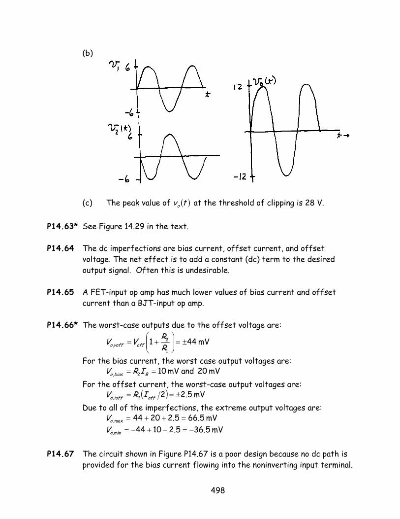
(b)
(c) The peak value of ( )tvo at the threshold of clipping is 28 V. P14.63* See Figure 14.29 in the text. P14.64 The dc imperfections are bias current, offset current, and offset
voltage. The net effect is to add a constant (dc) term to the desired output signal. Often this is undesirable.
P14.65 A FET-input op amp has much lower values of bias current and offset
current than a BJT-input op amp. P14.66* The worst-case outputs due to the offset voltage are:
mV 4411
2 ±=
+=
RRV,V offvoffo
For the bias current, the worst case output voltages are: mV 20 andmV 102 == B,biaso IRV For the offset current, the worst-case output voltages are: ( ) mV 5.222, ±== offioffo IRV Due to all of the imperfections, the extreme output voltages are: mV 5.665.22044max. =++=oV
mV 5.365.21044min, −=−+−=oV P14.67 The circuit shown in Figure P14.67 is a poor design because no dc path is
provided for the bias current flowing into the noninverting input terminal.
498
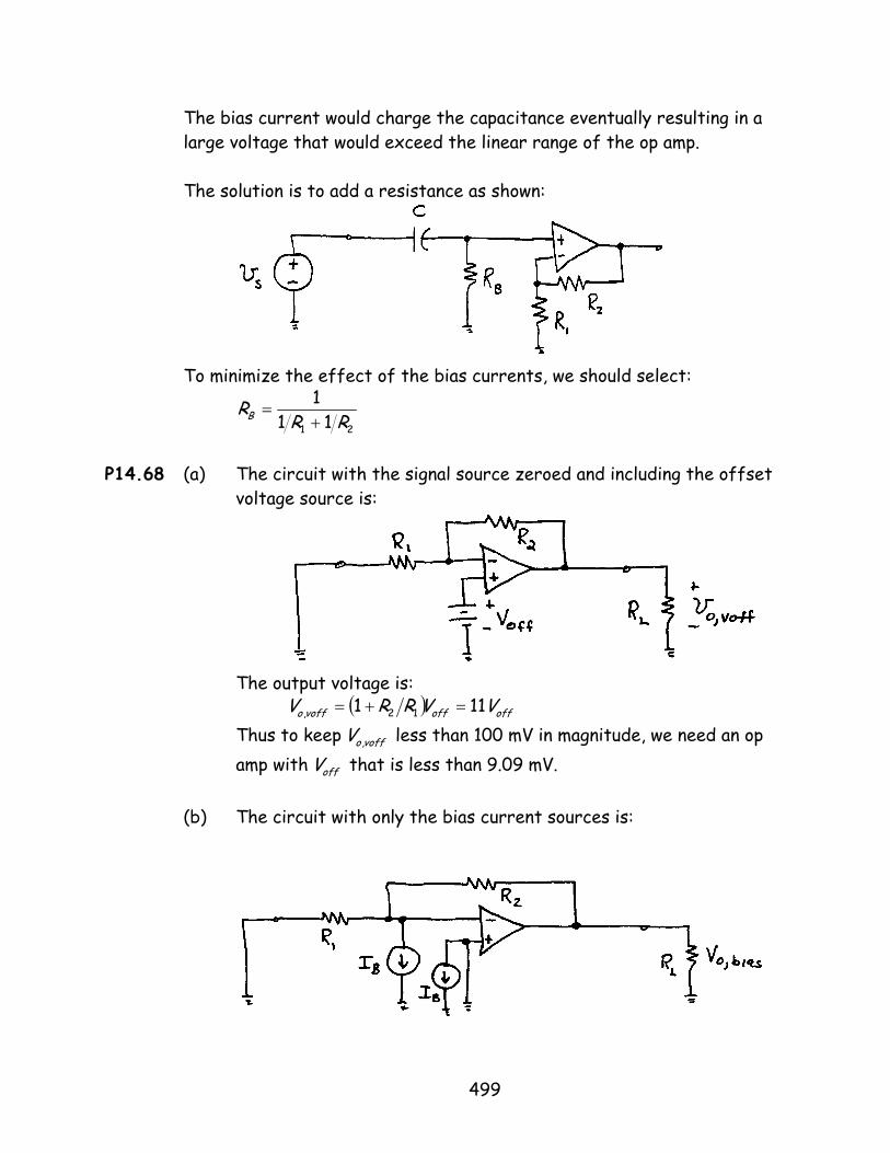
The bias current would charge the capacitance eventually resulting in a large voltage that would exceed the linear range of the op amp. The solution is to add a resistance as shown:
To minimize the effect of the bias currents, we should select:
21 11
1RR
RB +=
P14.68 (a) The circuit with the signal source zeroed and including the offset
voltage source is:
The output voltage is: ( ) offoffvoffo VVRRV 111 12, =+=
Thus to keep voffoV , less than 100 mV in magnitude, we need an op amp with offV that is less than 9.09 mV.
(b) The circuit with only the bias current sources is:
499

The output voltage is: biasbiaso IRV 2, =
Thus to keep biasoV , less than 100 mV in magnitude, we need an op amp with biasI less than 1µA.
(c) If we add a resistance Ω=+= k 09.9)/1/1/(1 21bias RRR in series
with the noninverting input terminal, the effects of the bias currents will cancel. The circuit is:
(d) With the resistance of part (c) in place, the output voltage due to
the offset current is: offioffo IRV 2, = Thus to keep ioffoV , less than 100 mV in magnitude, we need an op
amp with offI less than 1 µA. P14.69 The function of a differential amplifier is to produce an output that is
proportional to the differential input component and is independent of the common-mode component of the input.
P14.70* The circuit diagram is shown in Figure 14.33 in the text. To achieve a nominal gain of 10, we need to have R2 = 10R1. Values of R1 ranging from about 1 kΩ to 100 kΩ are practical. A good choice of values is R1 = 10 kΩ and R2 = 100 kΩ.
P14.71 The circuit diagram is shown in Figure 14.34 in the text. To achieve a
nominal gain of 10, we need to have R2 = 9R1. Values of R1 ranging from about 1 kΩ to 100 kΩ are good. A good choice of values is R1 = 20 kΩ andR2 = 180 kΩ. Any value of R in the range from 1 kΩ to 1 MΩ is acceptable.
500
P14.72 (a) The differential and common-mode components of the input signal are:
)2000cos(21 tvvvid = π=−)120cos(2)( 212
1cm tvvvi π=+=
(b) As discussed in the book, the first-stage gain for the differential signal is 1 12 /RR+ which for the values given is 10. On the other hand, the first-stage gain for the common-mode component is unity. Thus the output voltages are:
1 )120cos(2)2000cos(5 ttv outX ππ += )120cos(2)2000cos(51 ttv outX ππ +−=
(c) Assuming ideal op amps and perfectly matched components, the output
of the circuit is ( )( ) )2000cos(10/1) 2112( tvvRRtvo π=−+= P14.73 A running time integral is the integral for which the upper limit of
integration is time.
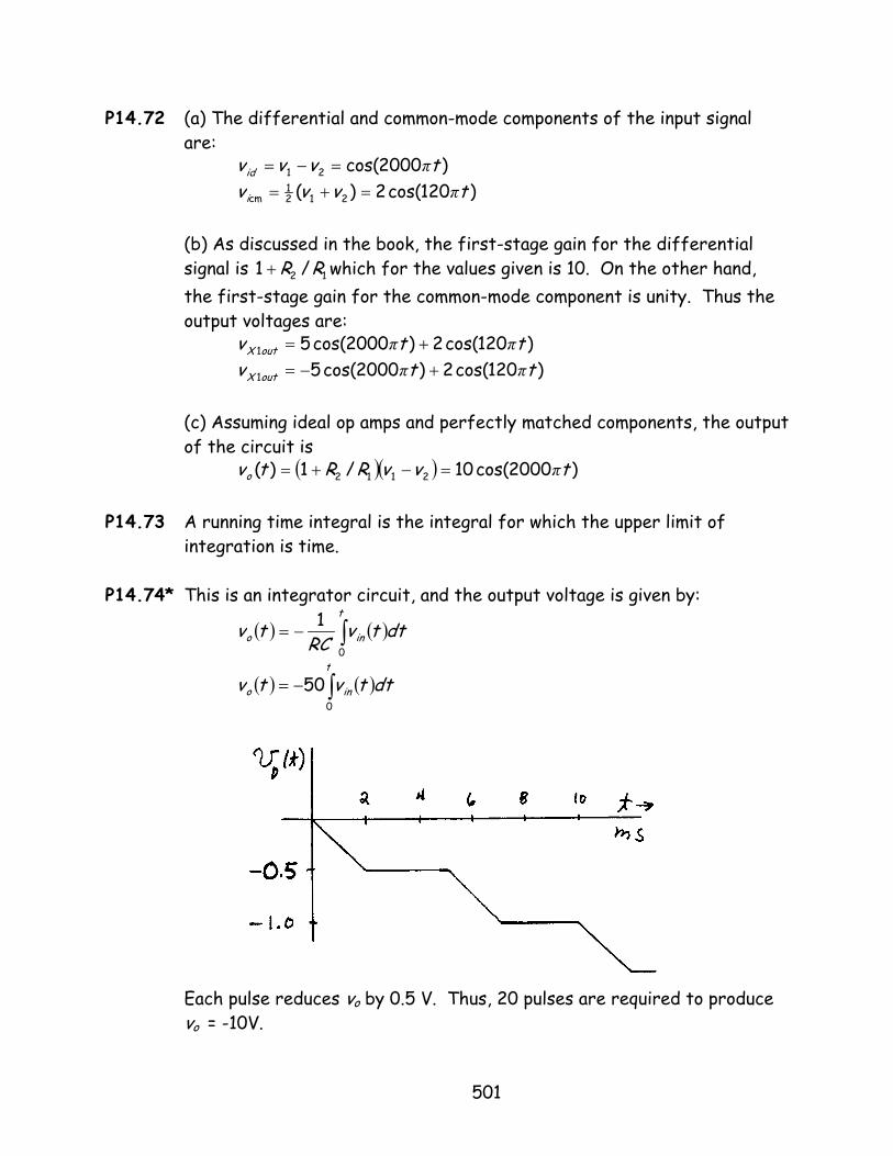
P14.74* This is an integrator circuit, and the output voltage is given by:
( ) ( )∫−=t
ino dttvRC
tv0
1
( ) ( )∫−=t
ino dttvtv0
50
Each pulse reduces vo by 0.5 V. Thus, 20 pulses are required to produce
vo = -10V.
501

P14.75 This is a differentiator circuit, and the output is given by:
( ) ( )dt
tdvRCtv ino −=
( )dt
tdvin310 −−=
A sketch of ( )tvo versus is:
P14.76 Let ( ) =tx displacement in meters. Then, we have
( ) ( )txtvin 100= and we want
( ) ( )dt
tdxtv =1 ( )dt
tdvin01.0=
and
( ) ( )2
2
2 dttxdtv = ( )
dttdv1=
A circuit that produces the desired voltages is:
We need 432211 and ,1 ,01.0 RRCRCR === . Suitable component values are:
502
Ω== M 121 RR F 01.01 µ=C F 0.12 µ=C Ω== k 1043 RR
P14.77 The function of a filter is to pass signal components in one frequency
range and reject components in another frequency range. A typical application is to remove noise from a signal of interest. An active filter is one that includes one or more op amps.
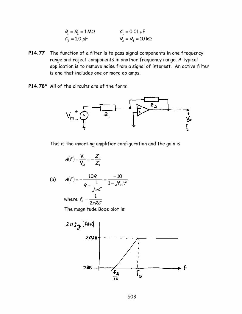
P14.78* All of the circuits are of the form:
This is the inverting amplifier configuration and the gain is
( )1
2
ZZfA
in
o −==VV
(a) ( )fjf
CjR
RfAB−
−=
+−=
110
110
ω
where RC
fB = π21
The magnitude Bode plot is:
503

(b) ( )
−−=+
−=ffj
RCjRfA B1/1 ω
where RC
fB = π21
The magnitude Bode plot is:
(c) ( )BfjfR
CjRfA+
−=+
−=1
111ω
where RC
fB 2=
π1
The magnitude Bode plot is:
P14.79 The gain is:
( )96.7/
111
jfRCjRCjfA −=−=−=
ωω
In decibels, the gain magnitude is
504
)96.7/log(20)(log20 ffA −= The sketch is:
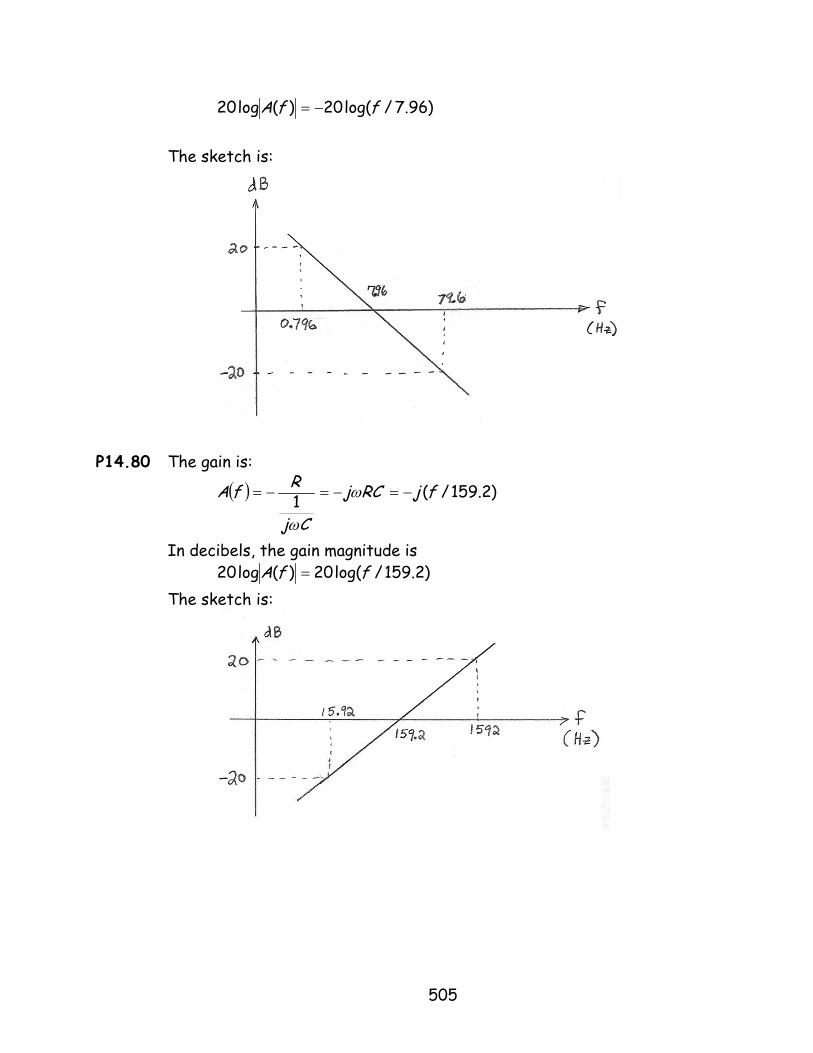
P14.80 The gain is:
( ) )2.159/(1 fjRCj
Cj
RfA −=−=−= ω
ω
In decibels, the gain magnitude is )2.159/log(20)(log20 ffA = The sketch is:
505
![M º b : U [ v q v . I b ] K 8 § v 3Ä < r K S . I b p 4 · [ ¼hamanomiya-es/matubbokuri/24_2.pdfM º b : U [ v q v . I b ] K 8 v 3Ä < r K S . I b p 4 · [ ¼ _4 [ 8 Ê ] v4) b](https://static.fdocuments.net/doc/165x107/5ae8aa587f8b9a290490705d/m-b-u-v-q-v-i-b-k-8-v-3-r-k-s-i-b-p-4-hamanomiya-esmatubbokuri242pdfm.jpg)


