Chapter 1 – Introduction VLSI Physical Design: From Graph ...
30
VLSI Physical Design: From Graph Partitioning to Timing Closure Chapter 1: Introduction 1 © KLMH Lienig Chapter 1 – Introduction Original Authors: Andrew B. Kahng, Jens Lienig, Igor L. Markov, Jin Hu VLSI Physical Design: From Graph Partitioning to Timing Closure
Transcript of Chapter 1 – Introduction VLSI Physical Design: From Graph ...
VLSI Physical Design: From Graph Partitioning to Timing Closure Chapter 1: Introduction 1
©KLMH
Lienig
Chapter 1 – Introduction
Original Authors:
Andrew B. Kahng, Jens Lienig, Igor L. Markov, Jin Hu
VLSI Physical Design: From Graph Partitioning to Timing Closure
VLSI Physical Design: From Graph Partitioning to Timing Closure Chapter 1: Introduction 2
©KLMH
Lienig
Chapter 1 – Introduction
1.1 Electronic Design Automation (EDA)
1.2 VLSI Design Flow
1.3 VLSI Design Styles
1.4 Layout Layers and Design Rules
1.5 Physical Design Optimizations
1.6 Algorithms and Complexity
1.7 Graph Theory Terminology
1.8 Common EDA Terminology
VLSI Physical Design: From Graph Partitioning to Timing Closure Chapter 1: Introduction 3
©KLMH
Lienig
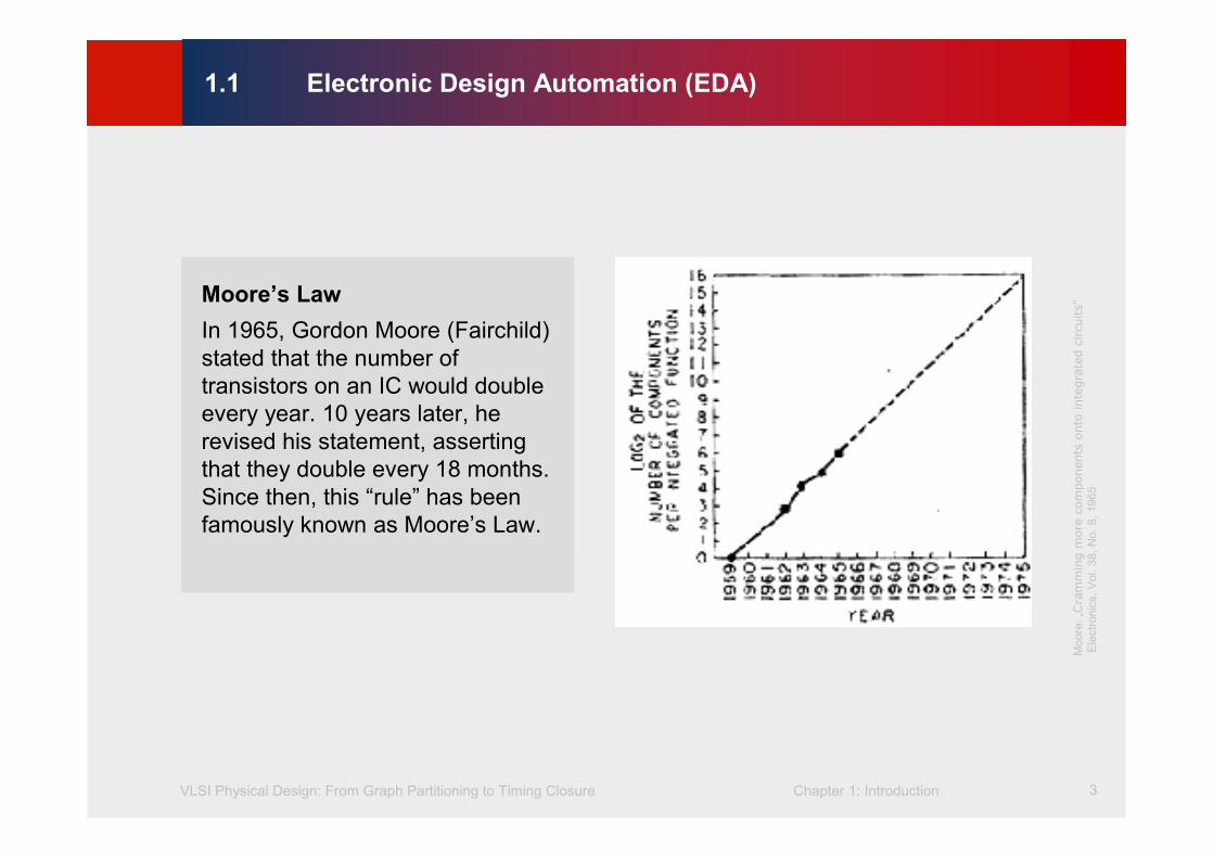
1.1 Electronic Design Automation (EDA)
Moore’s Law
In 1965, Gordon Moore (Fairchild)
stated that the number of
transistors on an IC would double
every year. 10 years later, he
revised his statement, asserting
that they double every 18 months.
Since then, this “rule” has been
famously known as Moore’s Law.
Moore: „Crammingmorecomponentsontointegratedcircuits"
Electronics, Vol. 38, No. 8, 1965
VLSI Physical Design: From Graph Partitioning to Timing Closure Chapter 1: Introduction 4
©KLMH
Lienig
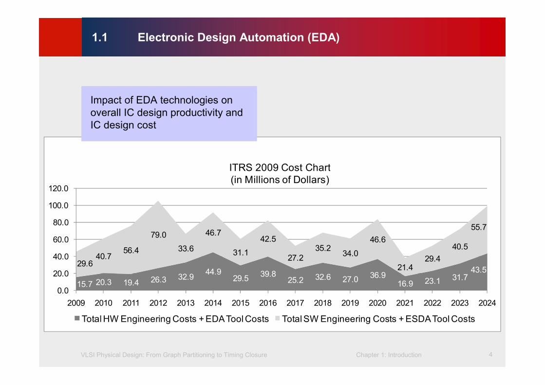
15.7 20.3 19.4 26.3 32.944.9
29.539.8
25.2 32.6 27.036.9
16.9 23.1 31.743.5
29.640.7
56.4
79.0
33.6
46.7
31.1
42.5
27.2
35.234.0
46.6
21.429.4
40.5
55.7
0.0
20.0
40.0
60.0
80.0
100.0
120.0
2009 2010 2011 2012 2013 2014 2015 2016 2017 2018 2019 2020 2021 2022 2023 2024
ITRS 2009 Cost Chart
(in Millions of Dollars)
Total HW Engineering Costs + EDA Tool Costs Total SW Engineering Costs + ESDA Tool Costs
ITRS 2009 Cost Chart
(in Millions of Dollars)
Total HW Engineering Costs + EDA Tool Costs Total SW Engineering Costs + ESDA Tool Costs
1.1 Electronic Design Automation (EDA)
Impact of EDA technologies on
overall IC design productivity and
IC design cost
VLSI Physical Design: From Graph Partitioning to Timing Closure Chapter 1: Introduction 5
©KLMH
Lienig
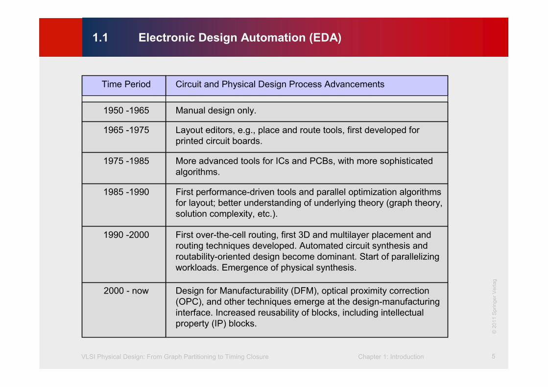
1.1 Electronic Design Automation (EDA)
Design for Manufacturability (DFM), optical proximity correction
(OPC), and other techniques emerge at the design-manufacturing
interface. Increased reusability of blocks, including intellectual
property (IP) blocks.
2000 - now
First over-the-cell routing, first 3D and multilayer placement and
routing techniques developed. Automated circuit synthesis and
routability-oriented design become dominant. Start of parallelizing
workloads. Emergence of physical synthesis.
1990 -2000
First performance-driven tools and parallel optimization algorithms
for layout; better understanding of underlying theory (graph theory,
solution complexity, etc.).
1985 -1990
More advanced tools for ICs and PCBs, with more sophisticated
algorithms.
1975 -1985
Layout editors, e.g., place and route tools, first developed for
printed circuit boards.
1965 -1975
Manual design only.1950 -1965
Circuit and Physical Design Process AdvancementsTime Period
©2011 Springer Verlag
VLSI Physical Design: From Graph Partitioning to Timing Closure Chapter 1: Introduction 6
©KLMH
Lienig
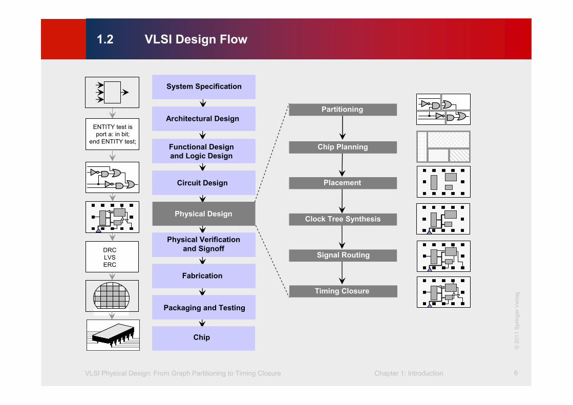
1.2 VLSI Design Flow
ENTITY test is
port a: in bit;
end ENTITY test;
DRC
LVS
ERC
Circuit Design
Functional Design
and Logic Design
Physical Design
Physical Verification
and Signoff
Fabrication
System Specification
Architectural Design
Chip
Packaging and Testing
Chip Planning
Placement
Signal Routing
Partitioning
Timing Closure
Clock Tree Synthesis
©2011 Springer Verlag
VLSI Physical Design: From Graph Partitioning to Timing Closure Chapter 1: Introduction 7
©KLMH
Lienig
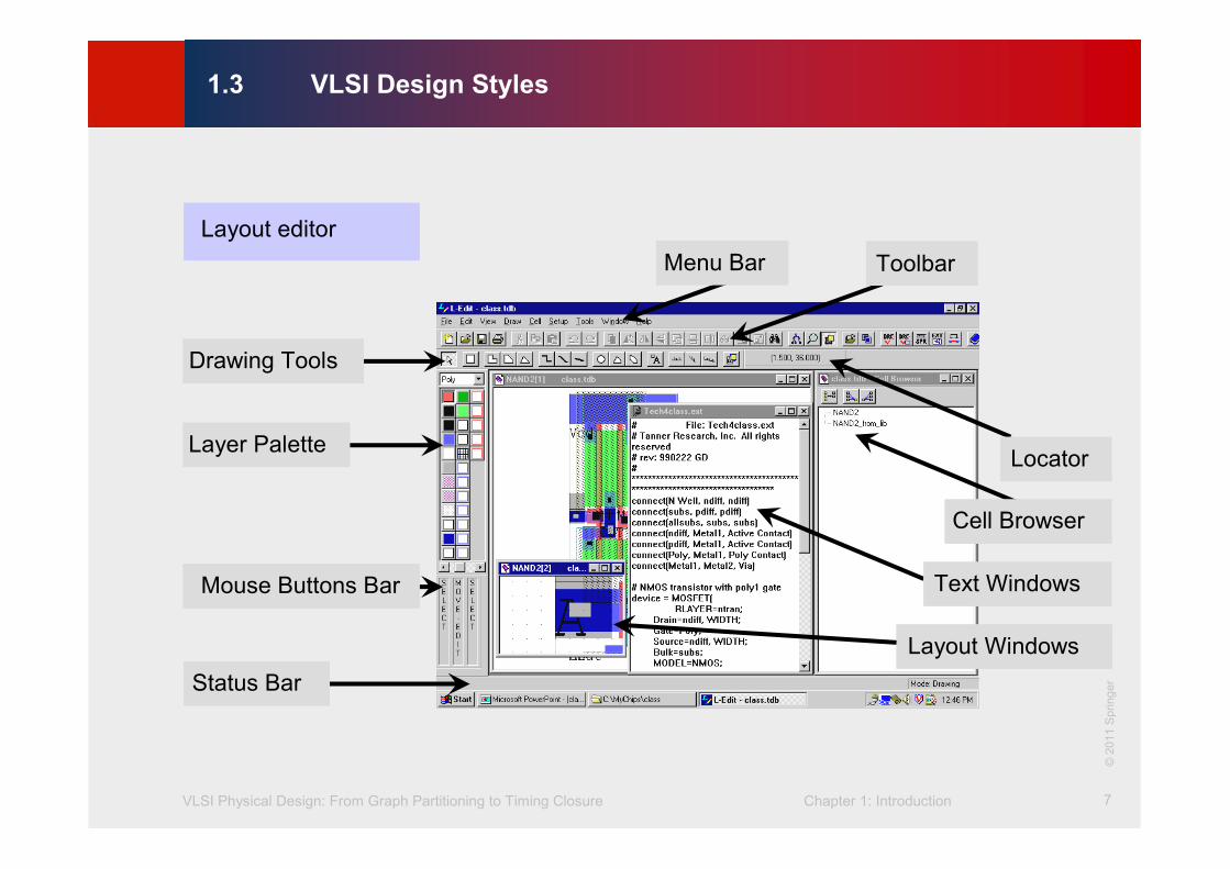
1.3 VLSI Design Styles
Layer Palette
Mouse Buttons Bar
Layout Windows
Drawing Tools
Cell Browser
Status Bar
ToolbarMenu Bar
Text Windows
Layout editor
Locator
©2011 Springer
VLSI Physical Design: From Graph Partitioning to Timing Closure Chapter 1: Introduction 8
©KLMH
Lienig
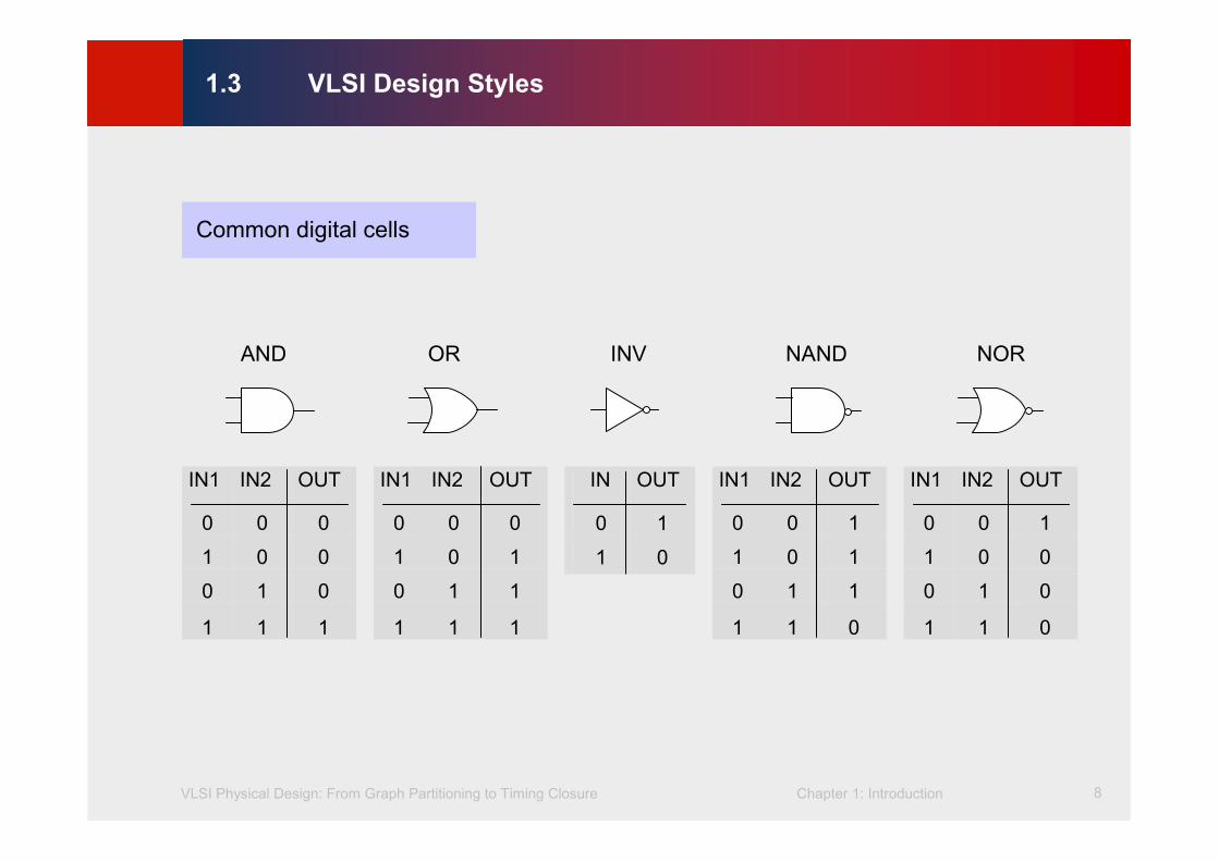
1.3 VLSI Design Styles
Common digital cells
11
01
01
10
OUTIN
OR INV NORNANDAND
111
010
001
000
OUTIN2IN1
111
110
101
000
OUTIN2IN1
011
010
001
100
OUTIN2IN1
011
110
101
100
OUTIN2IN1
VLSI Physical Design: From Graph Partitioning to Timing Closure Chapter 1: Introduction 9
©KLMH
Lienig
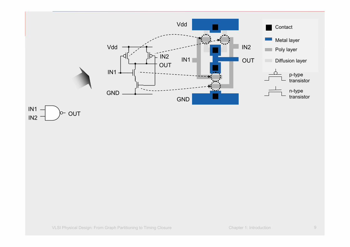
1.3 VLSI Design Styles
Vdd
GND
OUT
IN2
IN1OUT
IN2
IN1
OUTIN1
Vdd
GND
IN2
Contact
Diffusion layer
p-type
transistor
n-type
transistor
Metal layer
Poly layer
VLSI Physical Design: From Graph Partitioning to Timing Closure Chapter 1: Introduction 10
©KLMH
Lienig
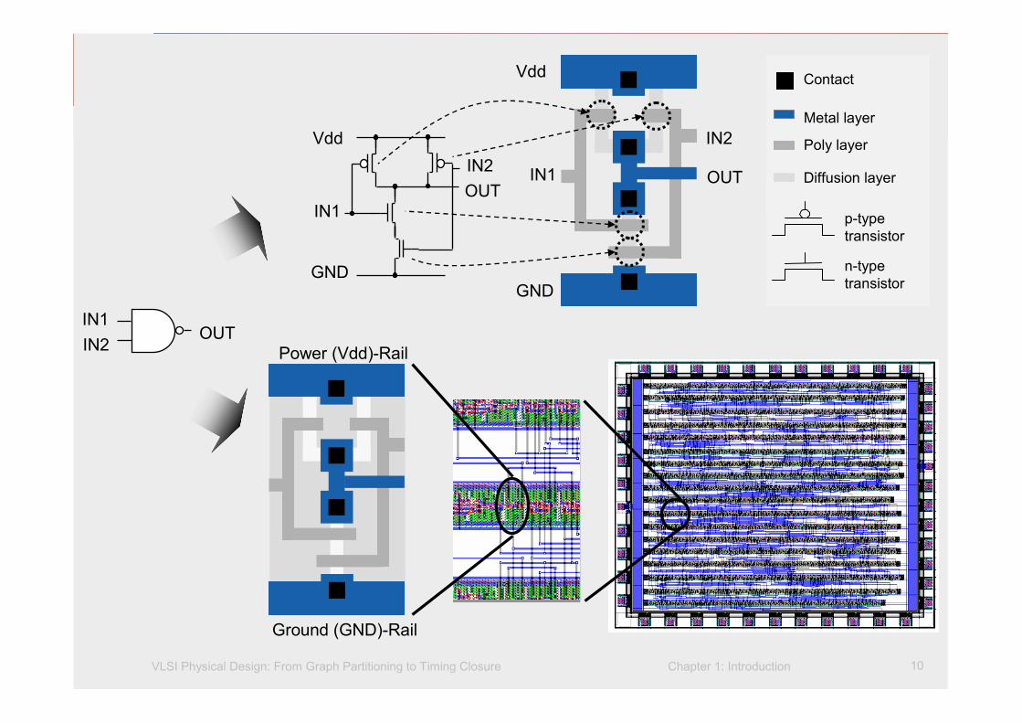
1.3 VLSI Design Styles
Power (Vdd)-Rail
Ground (GND)-Rail
Contact
Vdd
GND
OUT
IN2
IN1OUT
IN2
IN1
OUTIN1
Vdd
GND
IN2
Diffusion layer
p-type
transistor
n-type
transistor
Metal layer
Poly layer
VLSI Physical Design: From Graph Partitioning to Timing Closure Chapter 1: Introduction 11
©KLMH
Lienig
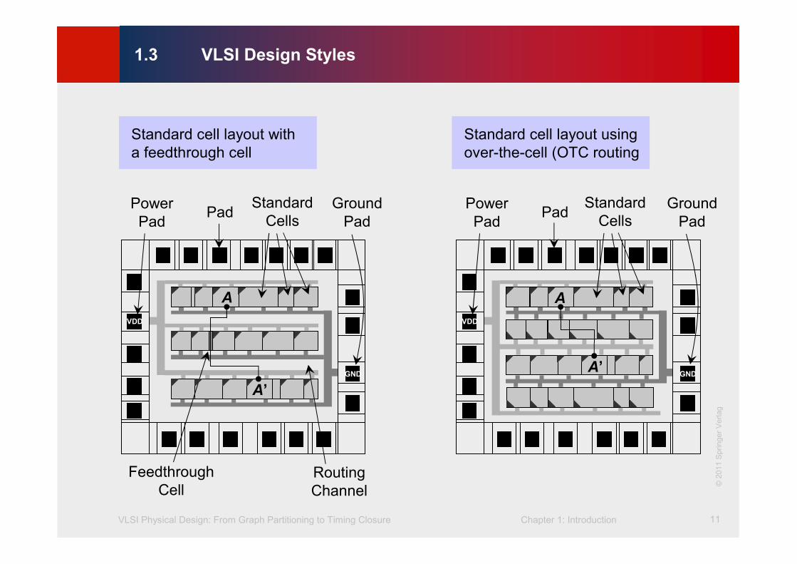
1.3 VLSI Design Styles
Standard cell layout with
a feedthrough cell
A
GND
Feedthrough
Cell
PadGround
Pad
Routing
Channel
Standard
CellsPower
Pad
GND
PadGround
Pad
Standard
CellsPower
Pad
A’
A
A’
VDD VDD
Standard cell layout using
over-the-cell (OTC routing
©2011 Springer Verlag
VLSI Physical Design: From Graph Partitioning to Timing Closure Chapter 1: Introduction 12
©KLMH
Lienig
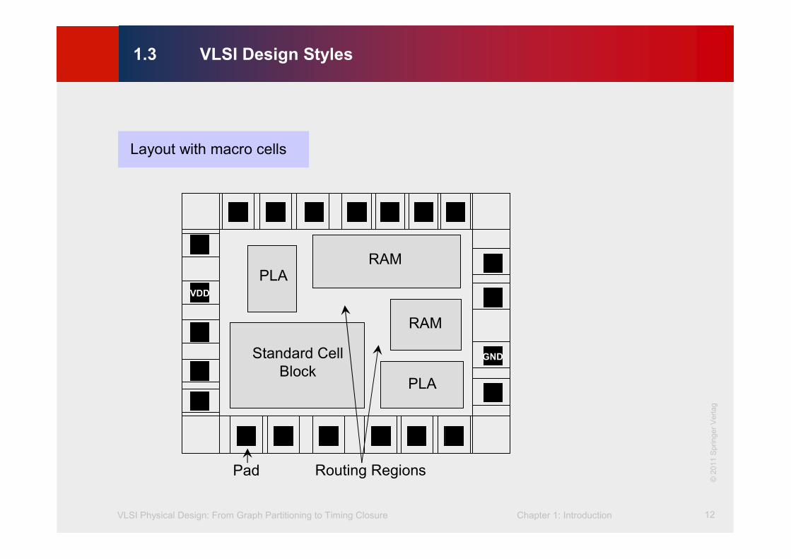
1.3 VLSI Design Styles
Layout with macro cells
Pad
GND
PLARAM
Standard Cell
Block
RAM
PLA
Routing Regions
VDD
©2011 Springer Verlag
VLSI Physical Design: From Graph Partitioning to Timing Closure Chapter 1: Introduction 13
©KLMH
Lienig
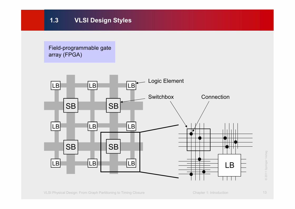
1.3 VLSI Design Styles
Field-programmable gate
array (FPGA)
LB LB LB
SB SB
LB LB LB
SB SB
LB LB LB
LB LB LB
SB SB
LB LB LB
SB SB
LB LB LB
LB LB
SB SB
LB LB LB
SB SB
LB LB LB
Logic Element
Switchbox
LB
Connection
©2011 Springer Verlag
VLSI Physical Design: From Graph Partitioning to Timing Closure Chapter 1: Introduction 14
©KLMH
Lienig
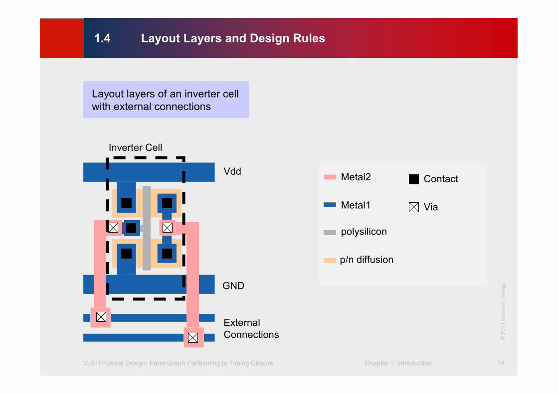
1.4 Layout Layers and Design Rules
Layout layers of an inverter cell
with external connections
Contact
Metal1
polysilicon
p/n diffusion
Vdd
GND
Via
Metal2
Inverter Cell
External
Connections ©2011 Springer Verlag
VLSI Physical Design: From Graph Partitioning to Timing Closure Chapter 1: Introduction 15
©KLMH
Lienig
1.4 Layout Layers and Design Rules
• Size rules, such as minimum width: The dimensions of any component (shape),
e.g., length of a boundary edge or area of the shape, cannot be smaller than given
minimum values. These values vary across different metal layers.
• Separation rules, such as minimum separation: Two shapes, either on the same
layer or on adjacent layers, must be a minimum (rectilinear or Euclidean diagonal)
distance apart.
• Overlap rules, such as minimum overlap: Two connected shapes on adjacent layers
must have a certain amount of overlap due to inaccuracy of mask alignment to
previously-made patterns on the wafer.
Categories of design rules

VLSI Physical Design: From Graph Partitioning to Timing Closure Chapter 1: Introduction 16
©KLMH
Lienig
1.4 Layout Layers and Design Rules
Categories of design rules
Minimum Width: a
Minimum Separation: b, c, d
Minimum Overlap: e
a
d
c
λ
b
e
λ: smallest meaningful technology-dependent unit of length
©2011 Springer Verlag
VLSI Physical Design: From Graph Partitioning to Timing Closure Chapter 1: Introduction 17
©KLMH
Lienig
1.5 Physical Design Optimizations
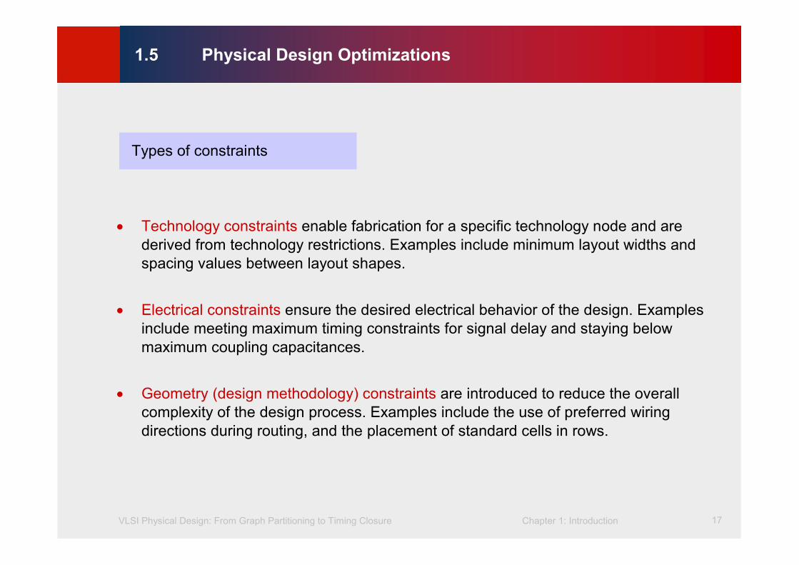
• Technology constraints enable fabrication for a specific technology node and are
derived from technology restrictions. Examples include minimum layout widths and
spacing values between layout shapes.
• Electrical constraints ensure the desired electrical behavior of the design. Examples
include meeting maximum timing constraints for signal delay and staying below
maximum coupling capacitances.
• Geometry (design methodology) constraints are introduced to reduce the overall
complexity of the design process. Examples include the use of preferred wiring
directions during routing, and the placement of standard cells in rows.
Types of constraints
VLSI Physical Design: From Graph Partitioning to Timing Closure Chapter 1: Introduction 18
©KLMH
Lienig
1.6 Algorithms and Complexity
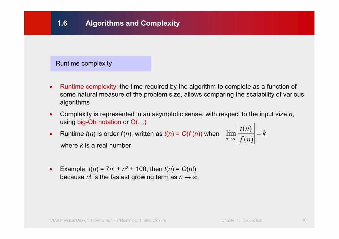
• Runtime complexity: the time required by the algorithm to complete as a function of
some natural measure of the problem size, allows comparing the scalability of various
algorithms
• Complexity is represented in an asymptotic sense, with respect to the input size n,
using big-Oh notation or O(…)
• Runtime t(n) is order f (n), written as t(n) = O(f (n)) when
where k is a real number
• Example: t(n) = 7n! + n2 + 100, then t(n) = O(n!)
because n! is the fastest growing term as n→ ∞.
Runtime complexity
knf
nt
n=
∞→ )(
)(lim
VLSI Physical Design: From Graph Partitioning to Timing Closure Chapter 1: Introduction 19
©KLMH
Lienig
1.6 Algorithms and Complexity
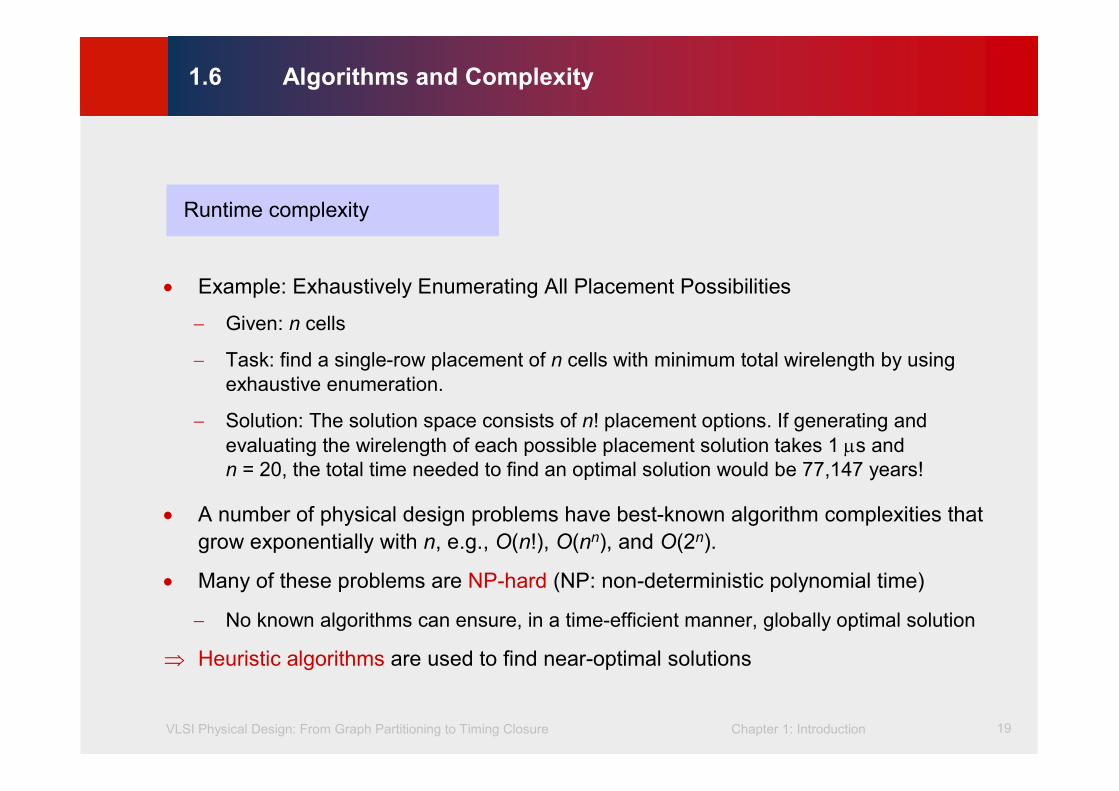
• Example: Exhaustively Enumerating All Placement Possibilities
− Given: n cells
− Task: find a single-row placement of n cells with minimum total wirelength by using
exhaustive enumeration.
− Solution: The solution space consists of n! placement options. If generating and
evaluating the wirelength of each possible placement solution takes 1 µs and
n = 20, the total time needed to find an optimal solution would be 77,147 years!
• A number of physical design problems have best-known algorithm complexities that
grow exponentially with n, e.g., O(n!), O(nn), and O(2n).
• Many of these problems are NP-hard (NP: non-deterministic polynomial time)
− No known algorithms can ensure, in a time-efficient manner, globally optimal solution
⇒ Heuristic algorithms are used to find near-optimal solutions
Runtime complexity
VLSI Physical Design: From Graph Partitioning to Timing Closure Chapter 1: Introduction 20
©KLMH
Lienig
1.6 Algorithms and Complexity
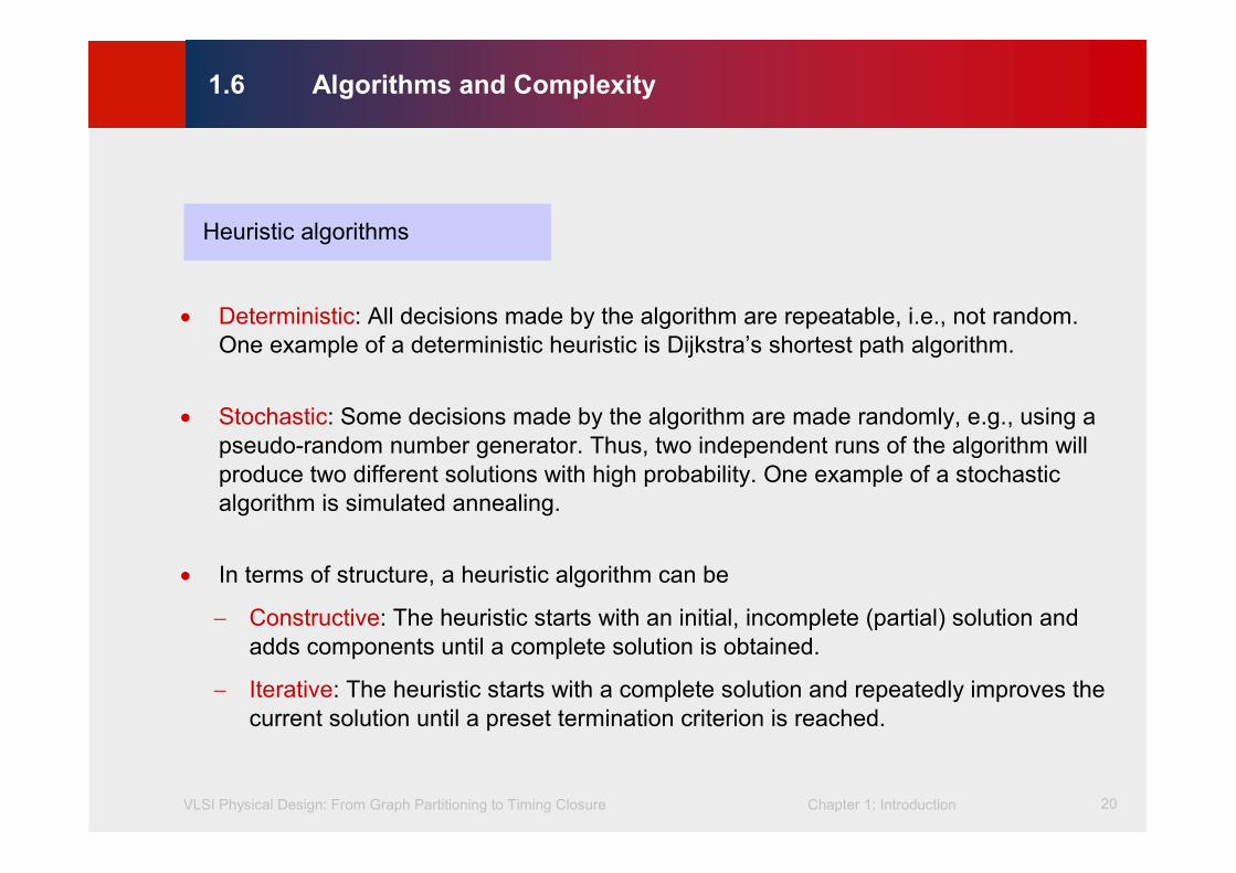
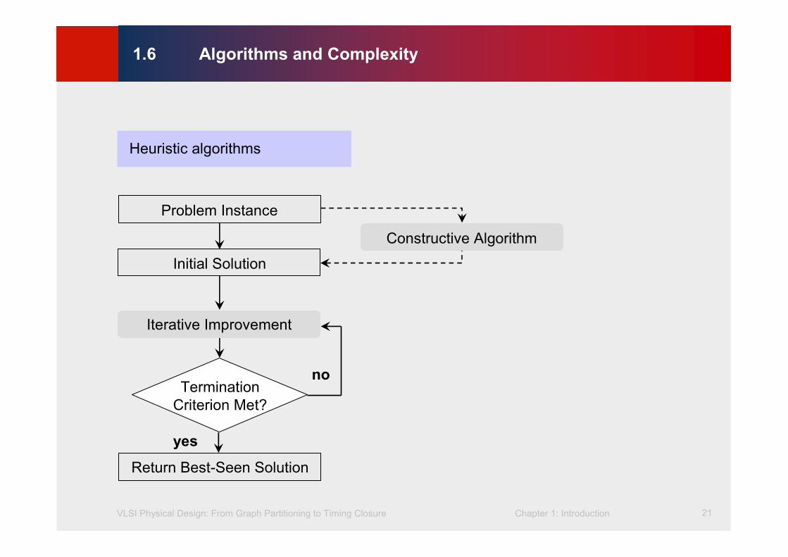
• Deterministic: All decisions made by the algorithm are repeatable, i.e., not random.
One example of a deterministic heuristic is Dijkstra’s shortest path algorithm.
• Stochastic: Some decisions made by the algorithm are made randomly, e.g., using a
pseudo-random number generator. Thus, two independent runs of the algorithm will
produce two different solutions with high probability. One example of a stochastic
algorithm is simulated annealing.
• In terms of structure, a heuristic algorithm can be
− Constructive: The heuristic starts with an initial, incomplete (partial) solution and
adds components until a complete solution is obtained.
− Iterative: The heuristic starts with a complete solution and repeatedly improves the
current solution until a preset termination criterion is reached.
Heuristic algorithms
VLSI Physical Design: From Graph Partitioning to Timing Closure Chapter 1: Introduction 21
©KLMH
Lienig
1.6 Algorithms and Complexity
Heuristic algorithms
Constructive Algorithm
Iterative Improvement
no
yes
Termination
Criterion Met?
Return Best-Seen Solution
Problem Instance
Initial Solution
VLSI Physical Design: From Graph Partitioning to Timing Closure Chapter 1: Introduction 22
©KLMH
Lienig
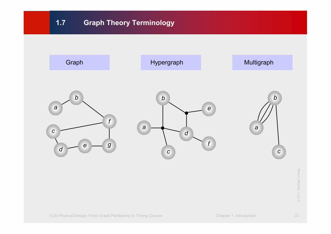
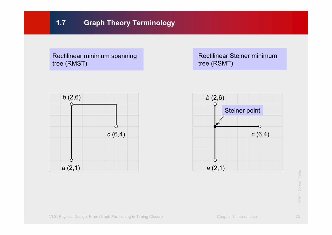
1.7 Graph Theory Terminology
Graph Hypergraph Multigraph
a
b
c
de
f
g
b
e
da
c
f
a
b
c
©2011 Springer Verlag
VLSI Physical Design: From Graph Partitioning to Timing Closure Chapter 1: Introduction 23
©KLMH
Lienig
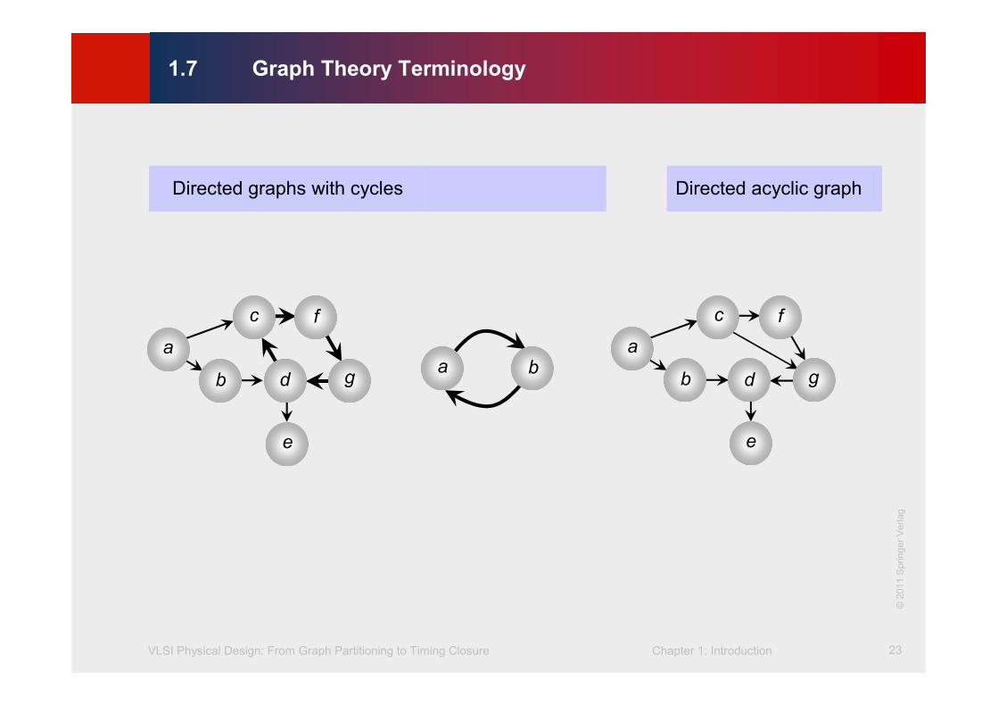
1.7 Graph Theory Terminology
Directed graphs with cycles Directed acyclic graph
c
a
b d
e
f
ga b
c
a
b d
e
f
g
©2011 Springer Verlag
VLSI Physical Design: From Graph Partitioning to Timing Closure Chapter 1: Introduction 24
©KLMH
Lienig
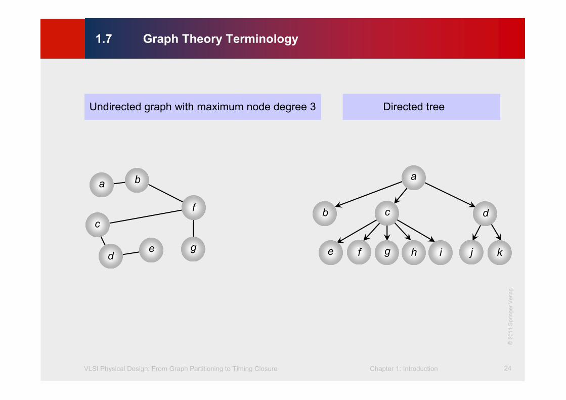
1.7 Graph Theory Terminology
Undirected graph with maximum node degree 3 Directed tree
a b
c
de
f
g
a
b c d
e f g h i j k
©2011 Springer Verlag
VLSI Physical Design: From Graph Partitioning to Timing Closure Chapter 1: Introduction 25
©KLMH
Lienig
1.7 Graph Theory Terminology
Rectilinear minimum spanning
tree (RMST)
Rectilinear Steiner minimum
tree (RSMT)
b (2,6)
a (2,1)
c (6,4) c (6,4)
Steiner point
b (2,6)
a (2,1)
©2011 Springer Verlag
VLSI Physical Design: From Graph Partitioning to Timing Closure Chapter 1: Introduction 26
©KLMH
Lienig
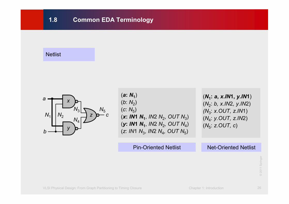
1.8 Common EDA Terminology
Netlist
a
b
x
y
z cN1 N2
N3
N4
(a: N1)
(b: N2)
(c: N5)
(x: IN1 N1, IN2 N2, OUT N3)
(y: IN1 N1, IN2 N2, OUT N4)
(z: IN1 N3, IN2 N4, OUT N5)
(N1: a, x.IN1, y.IN1)
(N2: b, x.IN2, y.IN2)
(N3: x.OUT, z.IN1)
(N4: y.OUT, z.IN2)
(N5: z.OUT, c)
Pin-Oriented Netlist Net-Oriented Netlist
N5
©2011 Springer
VLSI Physical Design: From Graph Partitioning to Timing Closure Chapter 1: Introduction 27
©KLMH
Lienig
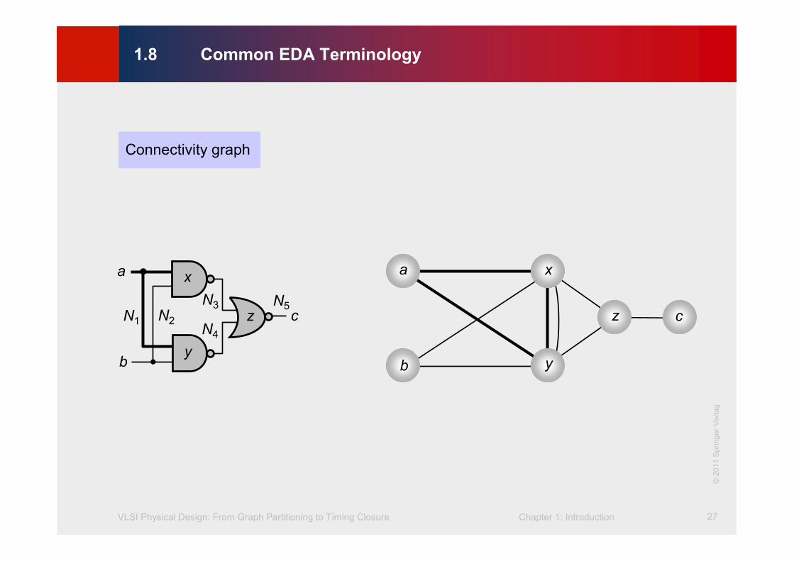
1.8 Common EDA Terminology
Connectivity graph
a
b
x
y
z cN1 N2
N3
N4
N5
a
b
x
y
z c
©2011 Springer Verlag
VLSI Physical Design: From Graph Partitioning to Timing Closure Chapter 1: Introduction 28
©KLMH
Lienig
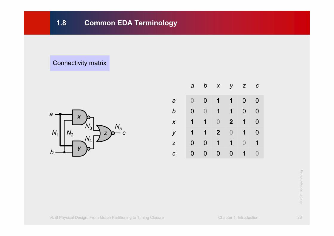
1.8 Common EDA Terminology
Connectivity matrix
a
b
x
y
z cN1 N2
N3
N4
N5
010000c
101100z
010211y
012011x
001100b
001100a
czyxba
©2011 Springer Verlag

VLSI Physical Design: From Graph Partitioning to Timing Closure Chapter 1: Introduction 29
©KLMH
Lienig
1.8 Common EDA Terminology
nnn
yyxxd 1212 −+−=
Distance metric between two points P1 (x1,y1) and P2 (x2,y2)
P1 (2,4)
P2 (6,1)
dM = 7
121221 ),( yyxxPPdM −+−=
dM = 7
with n = 2: Euclidean distance
n = 1: Manhattan distance
dE = 5
212
21221 )()(),( yyxxPPdE −+−=
VLSI Physical Design: From Graph Partitioning to Timing Closure Chapter 1: Introduction 30
©KLMH
Lienig
Summary of Chapter 1
• IC production experienced huge growth since the 1960s
− Exponential decrease in transistor size, cost per transistor, power per transistor, etc
• IC design is impossible without simplification and automation
− Row-based standard-cell layout with design rules
− Traditionally, each step in the VLSI design flow has been automated separately by
software (CAD) tools
• Software tools use sophisticated algorithms
− Many problems in physical design are NP-hard – solved by heuristic algorithms that
find near-optimal solutions
− Deterministic versus stochastic algorithms
− Constructive algorithms versus iterative improvement
− Graph algorithms – deal with circuit connectivity
− Computational geometry – deal with circuit layout