Chap18-Feedback, Stability and Oscillators
58
Jaeger/Blalock 3/10/04 Microelectronic Circuit Design McGraw-Hill Chapter 18 Feedback, Stability and Oscillators Microelectronic Circuit Design Richard C. Jaeger Travis N. Blalock Chap 18 - 1
-
Upload
manh-cuong-tran -
Category
Documents
-
view
241 -
download
0
Transcript of Chap18-Feedback, Stability and Oscillators
7/27/2019 Chap18-Feedback, Stability and Oscillators
http://slidepdf.com/reader/full/chap18-feedback-stability-and-oscillators 1/58
Jaeger/Blalock 3/10/04
Microelectronic Circuit DesignMcGraw-Hill
Chapter 18
Feedback, Stability and Oscillators
Microelectronic Circuit Design
Richard C. Jaeger
Travis N. Blalock
Chap 18 - 1
7/27/2019 Chap18-Feedback, Stability and Oscillators
http://slidepdf.com/reader/full/chap18-feedback-stability-and-oscillators 2/58
Jaeger/Blalock 3/10/04
Microelectronic Circuit DesignMcGraw-Hill
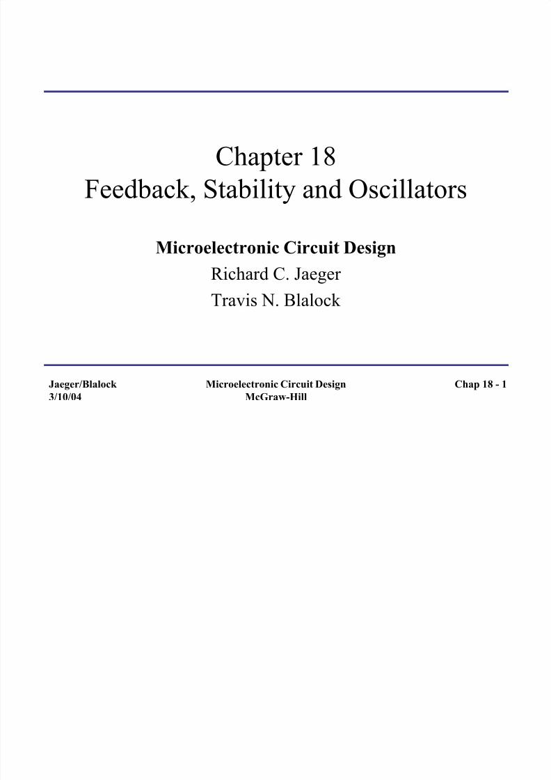
Chapter Goals
• Review concepts of negative and positive feedback.
• Develop two-port approach to analysis of negative feedback amplifiers.
• Understand topologies and characteristics of series-shunt, shunt-shunt, shunt-series and series-series feedback configurations.
• Discuss common errors that occur in applying two-port feedback theory.• Discuss effects of feedback on frequency response and feedback amplifier
stability and interpret stability in in terms of Nyquist and Bode plots.
• Use SPICE ac and transfer function analyses on feedback amplifiers.
• Determine loop-gain of closed-loop amplifiers using SPICE simulation or measurement.
• Discuss Barkhausen criteria for oscillation and amplitude stabilization• Understand basic RC, LC and crystal oscillator circuits and present LCR model
of quartz crystal.
Chap 18 - 2
7/27/2019 Chap18-Feedback, Stability and Oscillators
http://slidepdf.com/reader/full/chap18-feedback-stability-and-oscillators 3/58
Jaeger/Blalock 3/10/04
Microelectronic Circuit DesignMcGraw-Hill
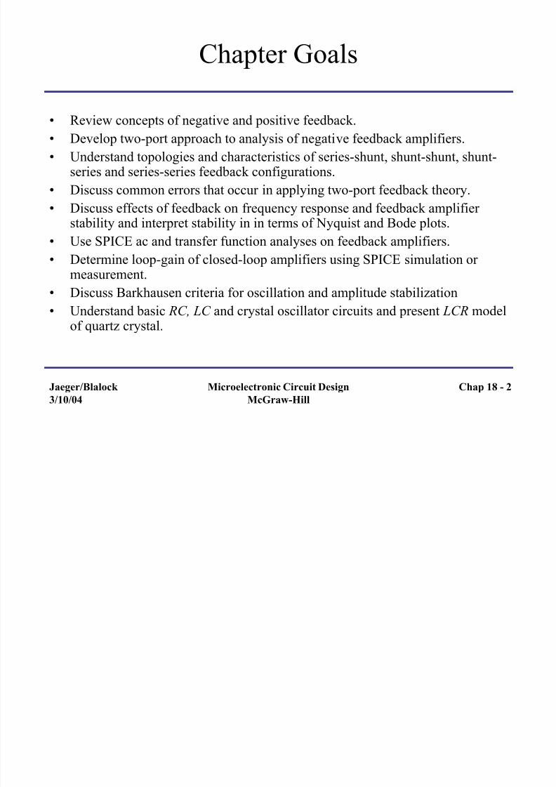
Feedback Effects
• Gain Stability: Feedback reduces sensitivity of gain to variations in
values of transistor parameters and circuit elements.
• Input and Output Impedances: Feedback can increase or decrease input
and output resistances of an amplifier.
• Bandwidth: Bandwidth of amplifier can be extended using feedback.
• Nonlinear Distortion: Feedback reduces effects of nonlinear distortion.eg: removal of dead zone in class-B amplifiers
Chap 18 - 3
7/27/2019 Chap18-Feedback, Stability and Oscillators
http://slidepdf.com/reader/full/chap18-feedback-stability-and-oscillators 4/58
Jaeger/Blalock 3/10/04
Microelectronic Circuit DesignMcGraw-Hill
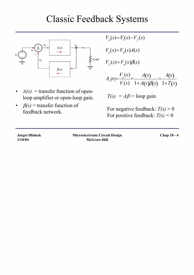
Classic Feedback Systems
• A(s) = transfer function of open-
loop amplifier or open-loop gain.
• b (s) = transfer function of
feedback network.
V d ( s)V
i( s)V
f ( s)
V o( s)V
d ( s) A( s)
V f ( s)V
o( s) b ( s)
Av
s V
o( s)
V i( s)
A s
1 A s b s
A s 1T s
T(s) = A b = loop gain
For negative feedback: T(s) > 0
For positive feedback: T(s) < 0
Chap 18 - 4
7/27/2019 Chap18-Feedback, Stability and Oscillators
http://slidepdf.com/reader/full/chap18-feedback-stability-and-oscillators 5/58
Jaeger/Blalock 3/10/04
Microelectronic Circuit DesignMcGraw-Hill
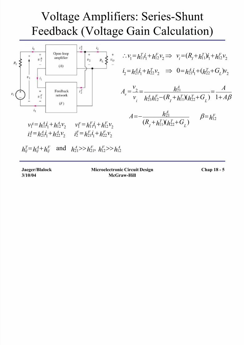
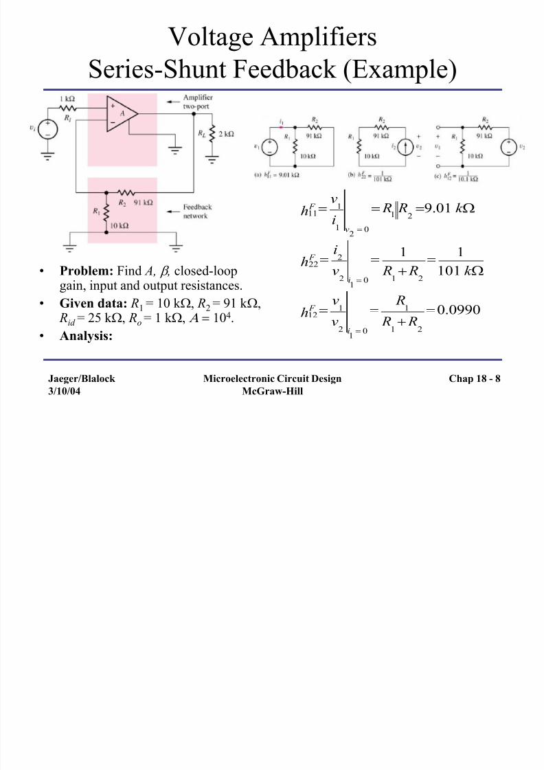
Voltage Amplifiers: Series-Shunt
Feedback (Voltage Gain Calculation)
1
A
v
11
A
hi1
12
A
hv
2
1
F
v
11
F
hi1
12
F
hv
2
2 Ai 21
Ah i1 22
Ah v2 2
F i 21 F h i
1 22
F h v2
ijT h ij
Ah ij F h and 21
Ah 21 F h , 12
F h 12 Ah
v1 11
T h i1 12
F h v2
vi( R
I 11
T h )i1 12
F h v2
i2 21
Ah i1 22
T h v2 0 21
Ah i1( 22
T h G L
)v2
Av v
2
vi
21 Ah
21 Ah 12
F h ( R I
11T h )( 22
T h G L
) A
1 A b
A 21 Ah
( R I
11T h )( 22
T h G L
) b 12
F h
Chap 18 - 5
7/27/2019 Chap18-Feedback, Stability and Oscillators
http://slidepdf.com/reader/full/chap18-feedback-stability-and-oscillators 6/58
Jaeger/Blalock 3/10/04
Microelectronic Circuit DesignMcGraw-Hill
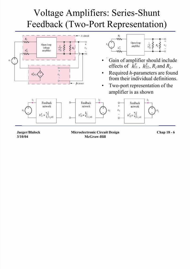
Voltage Amplifiers: Series-Shunt
Feedback (Two-Port Representation)
• Gain of amplifier should include
effects of , , R I and R L.• Required h-parameters are found
from their individual definitions.
• Two-port representation of the
amplifier is as shown
11 F
h
22 F
h
Chap 18 - 6
7/27/2019 Chap18-Feedback, Stability and Oscillators
http://slidepdf.com/reader/full/chap18-feedback-stability-and-oscillators 7/58
Jaeger/Blalock 3/10/04
Microelectronic Circuit DesignMcGraw-Hill
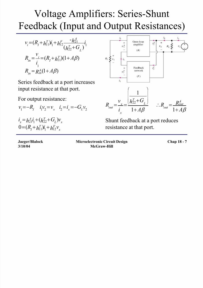
Voltage Amplifiers: Series-Shunt
Feedback (Input and Output Resistances)
vi( R
I 11
T h )i1
12 F h
- 21 Ah
( 22T h G
L)
i1
Rin
v
i
i1
( R I
11T h )(1 A b )
Rin in A R (1 A b )
Series feedback at a port increases
input resistance at that port.
For output resistance:
v1 R I i1v2 v x i2 i x G Lv2
i x
21 Ah i
1( 22
T h G L
)v x
0 ( R I
11T h )i
1 12
F h v x
Rout
v x
i x
1
22T h G
L
1 A b Rout out A R
1 A b
Shunt feedback at a port reduces
resistance at that port.
Chap 18 - 7
7/27/2019 Chap18-Feedback, Stability and Oscillators
http://slidepdf.com/reader/full/chap18-feedback-stability-and-oscillators 8/58
7/27/2019 Chap18-Feedback, Stability and Oscillators
http://slidepdf.com/reader/full/chap18-feedback-stability-and-oscillators 9/58
Jaeger/Blalock 3/10/04
Microelectronic Circuit DesignMcGraw-Hill
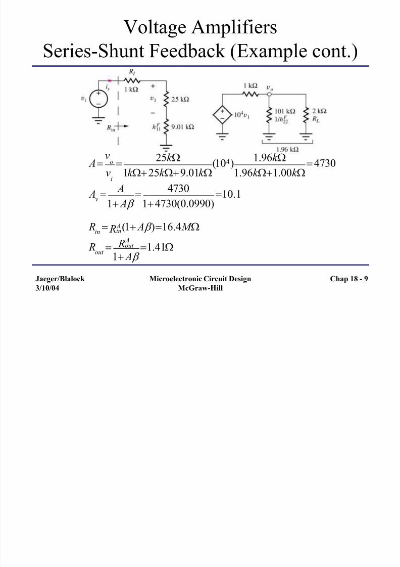
Voltage Amplifiers
Series-Shunt Feedback (Example cont.)
Av
o
vi
25k W1k W 25k W9.01k W
(104)1.96k W
1.96k W1.00k W 4730
Av A
1 A b 4730
1 4730(0.0990)10.1
Rin
in A R (1 A b )16.4 M W
Rout
out A R
1 A b 1.41W
Chap 18 - 9
7/27/2019 Chap18-Feedback, Stability and Oscillators
http://slidepdf.com/reader/full/chap18-feedback-stability-and-oscillators 10/58
Jaeger/Blalock 3/10/04
Microelectronic Circuit DesignMcGraw-Hill
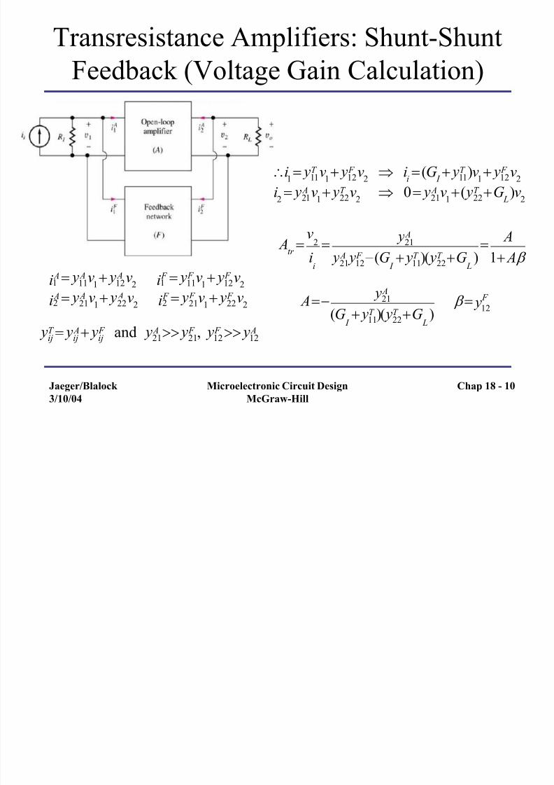
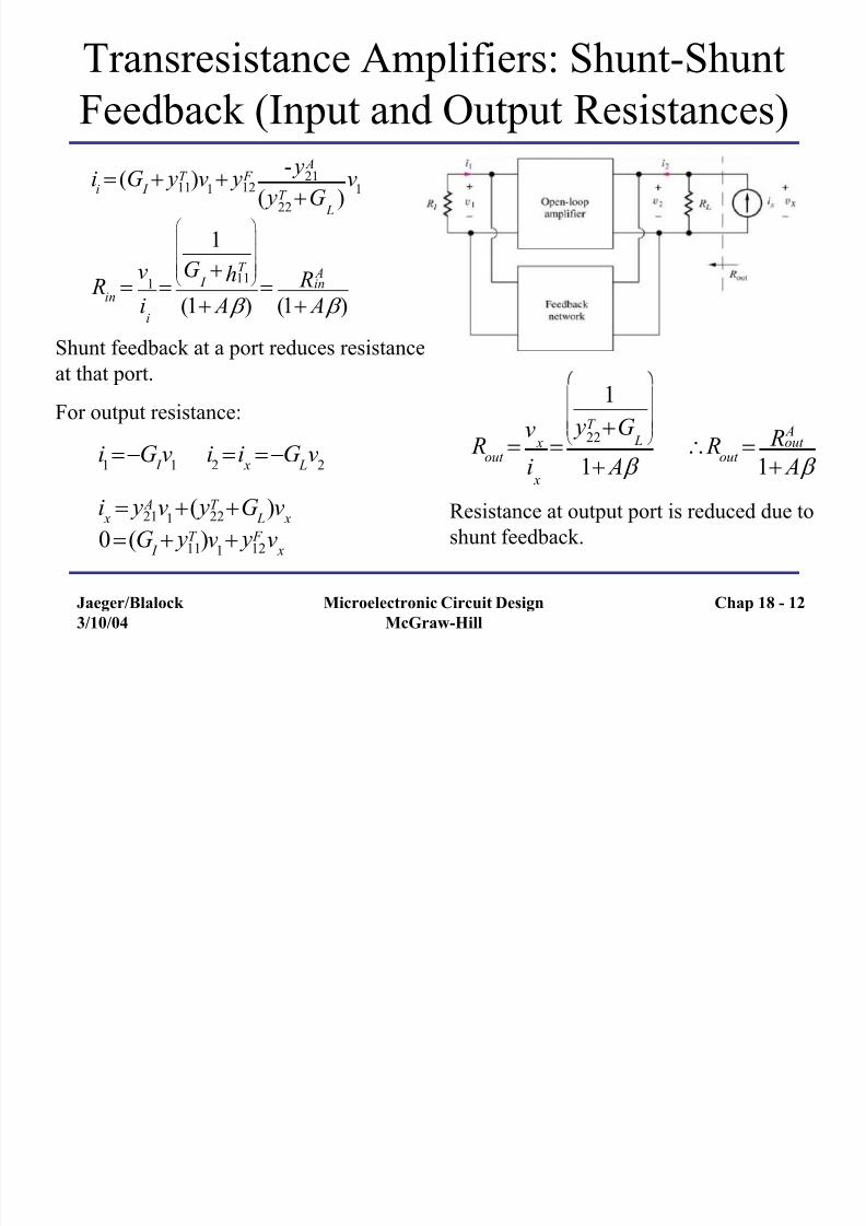
Transresistance Amplifiers: Shunt-Shunt
Feedback (Voltage Gain Calculation)
1 Ai 11
A y v1 12
A y v2 1
F i 11 F y v
1 12
F y v2
2 Ai 21
A y v1 22
A y v2 2
F i 21 F y v
1 22 F y v
2
ijT y ij
A y ij F y and 21
A y 21 F y , 12
F y 12 A y
i1 11
T y v1 12
F y v2 i
i (G
I 11
T y )v1 12
F y v2
i2 21 A y v1 22T y v2 0 21 A y v1( 22T y G L)v2
Atr
v2
ii
21 A y
21 A y
12 F y (G
I 11
T y )( 22T y G
L)
A
1 A b
A 21 A y
(G I
11T y )( 22
T y G L) b
12
F y
Chap 18 - 10
7/27/2019 Chap18-Feedback, Stability and Oscillators
http://slidepdf.com/reader/full/chap18-feedback-stability-and-oscillators 11/58
Jaeger/Blalock 3/10/04
Microelectronic Circuit DesignMcGraw-Hill
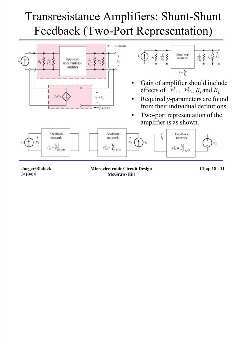
Transresistance Amplifiers: Shunt-Shunt
Feedback (Two-Port Representation)
• Gain of amplifier should includeeffects of , , R I and R L.
• Required y-parameters are foundfrom their individual definitions.
• Two-port representation of theamplifier is as shown.
11 F y
22 F y
Chap 18 - 11
7/27/2019 Chap18-Feedback, Stability and Oscillators
http://slidepdf.com/reader/full/chap18-feedback-stability-and-oscillators 12/58
Jaeger/Blalock 3/10/04
Microelectronic Circuit DesignMcGraw-Hill
Transresistance Amplifiers: Shunt-Shunt
Feedback (Input and Output Resistances)
ii (G
I 11
T y )v1 12
F y-
21 A y
(22T y G
L)
v1
Rin
v
1
ii
1
G I
11T h
(1 A b ) in
A R
(1 A b )
Shunt feedback at a port reduces resistance
at that port.
For output resistance:
i1 G I v1 i2 i x G Lv2
i x
21 A y v
1( 22
T y G L
)v x
0(G I
11T y )v
1 12
F y v x
Rout
v x
i x
1
22T y G
L
1 A b Rout out A R
1 A b
Resistance at output port is reduced due to
shunt feedback.
Chap 18 - 12
7/27/2019 Chap18-Feedback, Stability and Oscillators
http://slidepdf.com/reader/full/chap18-feedback-stability-and-oscillators 13/58
Jaeger/Blalock 3/10/04
Microelectronic Circuit DesignMcGraw-Hill
Transresistance Amplifiers
Shunt-Shunt Feedback (Example)
• Problem: Find A, b , closed-loop
gain, input and output resistances.
• Given data: V A = 50 V, b F = 150
• Analysis: For the dc equivalent
circuit,
11 F
y
i1
v1 v
2 0
1
R F
10-5
S
22 F y
i2
v2 i
2 0
1
R F
10-5 S
12 F y
i1
v2 v1
0
1
R F
10-5 S
I C
V
CC V
BE
RC
R
C R
F
b F
0.970 mA
V CE
V CC
( I C
I B
) RC
1.35 V
g m
40(0.977mA)39.1 mS
r
1
g m
3.84 k W r o
50V 1.35V
0.977mA52.6 k W
Chap 18 - 13
7/27/2019 Chap18-Feedback, Stability and Oscillators
http://slidepdf.com/reader/full/chap18-feedback-stability-and-oscillators 14/58
Jaeger/Blalock 3/10/04
Microelectronic Circuit DesignMcGraw-Hill
Transresistance Amplifiers
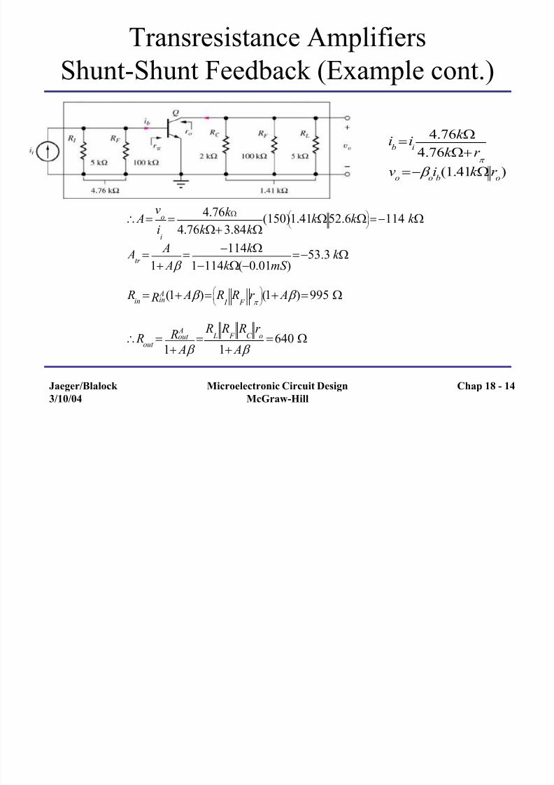
Shunt-Shunt Feedback (Example cont.)
Av
o
ii
4.76k W
4.76k W 3.84k W(150)1.41k W 52.6k W
114 k W
Atr
A
1 A b 114k W
1114k W(0.01mS )53.3 k W
Rin in A R (1 A b ) R
I R
F r
(1 A b ) 995 W
Rout
out A R
1 A b
R L
R F
RC
r o
1 A b 640 W
ib ii
4.76k W
4.76k Wr
vo b oib(1.41k Wr
o)
Chap 18 - 14
7/27/2019 Chap18-Feedback, Stability and Oscillators
http://slidepdf.com/reader/full/chap18-feedback-stability-and-oscillators 15/58
Jaeger/Blalock 3/10/04
Microelectronic Circuit DesignMcGraw-Hill
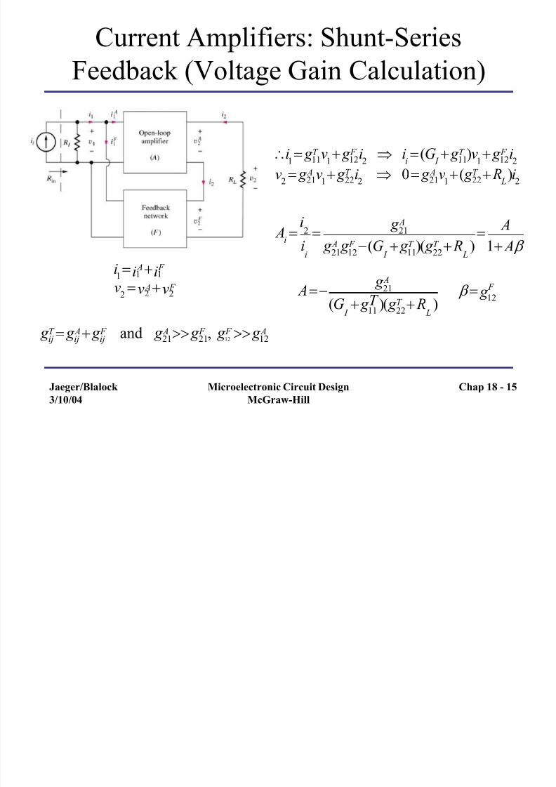
Current Amplifiers: Shunt-Series
Feedback (Voltage Gain Calculation)
i1 1
Ai 1 F i
v2 2 Av 2 F v
ijT g ij
A g ij F g and 21
A g 21 F g ,
12
F g 12 A g
i1 11
T g v1 12
F g i2 i
i (G
I 11
T g )v1 12
F g i2
v2 21
A g v1 22
T g i2 0 21
A g v1( 22
T g R L
)i2
Ai
i2
ii
21 A g
21 A g
12 F g (G
I
11T g )(
22T g R
L) A
1 A b
A 21
A g
(G I
11T g )(
22T g R
L) b 12
F
g
Chap 18 - 15
7/27/2019 Chap18-Feedback, Stability and Oscillators
http://slidepdf.com/reader/full/chap18-feedback-stability-and-oscillators 16/58
Jaeger/Blalock 3/10/04
Microelectronic Circuit DesignMcGraw-Hill
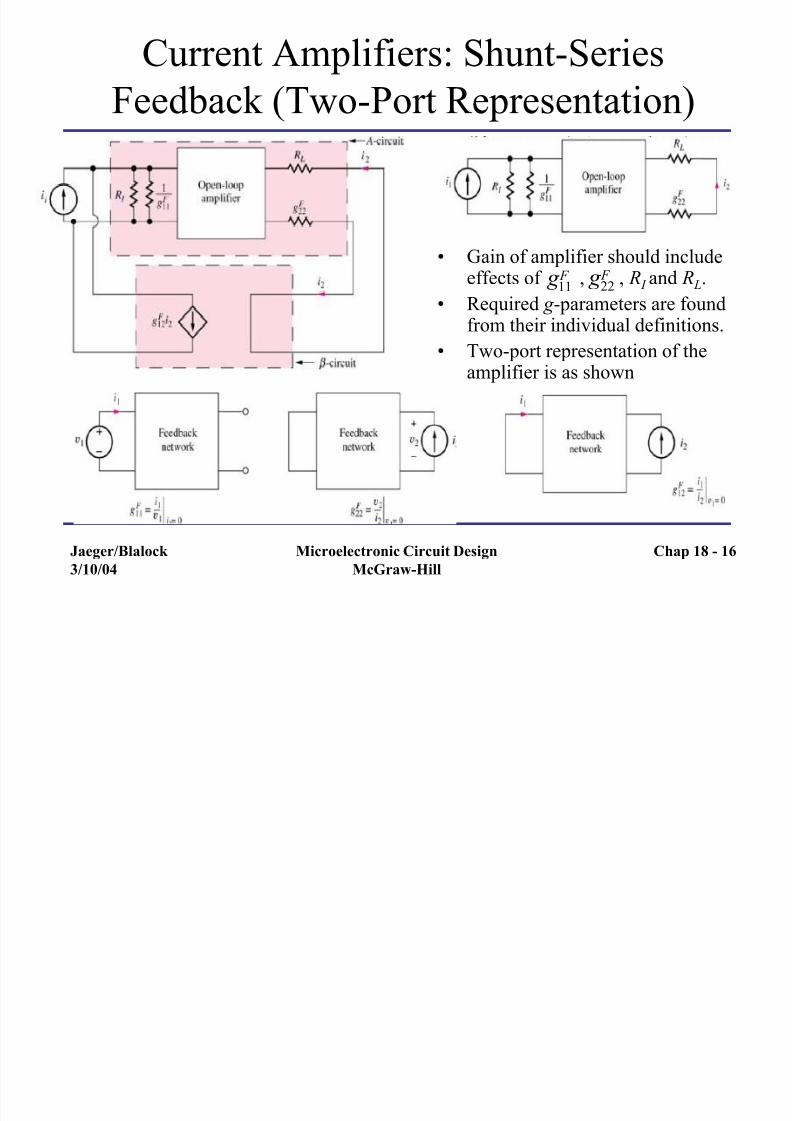
Current Amplifiers: Shunt-Series
Feedback (Two-Port Representation)
• Gain of amplifier should include
effects of , , R I and R L.• Required g -parameters are found
from their individual definitions.
• Two-port representation of theamplifier is as shown
11 F g
22 F g
Chap 18 - 16
7/27/2019 Chap18-Feedback, Stability and Oscillators
http://slidepdf.com/reader/full/chap18-feedback-stability-and-oscillators 17/58
Jaeger/Blalock 3/10/04
Microelectronic Circuit DesignMcGraw-Hill
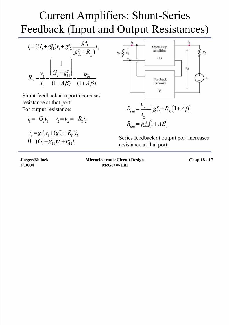
Current Amplifiers: Shunt-Series
Feedback (Input and Output Resistances)
ii(G
I 11
T g )v1 12
F g - 21
A g
(22T g R
L)
v1
Rin
v1
ii
1
G I
11T g
(1 A b ) in A R
(1 A b )
Shunt feedback at a port decreases
resistance at that port.
For output resistance:
Rout
v
x
i2
22T g R
L
1 A b
Rout out
A R 1 A b
Series feedback at output port increases
resistance at that port.
i1 G I v1 v2 v x R Li2
v x
21 A g v
1( 22
T g R L
)i2
0(G I
11T g )v
1 12
F g i2
Chap 18 - 17
7/27/2019 Chap18-Feedback, Stability and Oscillators
http://slidepdf.com/reader/full/chap18-feedback-stability-and-oscillators 18/58
Jaeger/Blalock 3/10/04
Microelectronic Circuit DesignMcGraw-Hill
Transconductance Amplifiers: Series-Series
Feedback (Voltage Gain Calculation)
v1 1 Av 1 F vv
2
2 Av
2 F v
ijT z ij
A z ij F z and
21 A z 21
F z ,12 F z 12
A z
v1 11
T z i1 12
T z i2 v
i( R
S 11
T z )i1 12
F z i2
v2 21
T z i1 22
T z i2 0 21
T z i1(
22T z R
L)i
2
Atc
i2
vi
21 A z
21 A z 12
F z ( R I
11T z )( 22
T z R L
) A
1 A b
A 21 A z ( R
I
11T z )( 22
T z R L
) b z
12 F
Chap 18 - 18
7/27/2019 Chap18-Feedback, Stability and Oscillators
http://slidepdf.com/reader/full/chap18-feedback-stability-and-oscillators 19/58
Jaeger/Blalock 3/10/04
Microelectronic Circuit DesignMcGraw-Hill
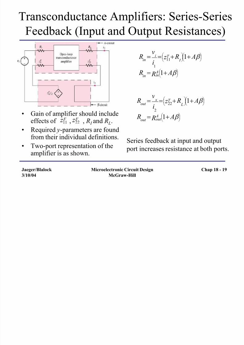
Transconductance Amplifiers: Series-Series
Feedback (Input and Output Resistances)
Rout
v
x
i2
22T z R
L
1 A b
Rout
out A R 1 A b
Rin
v
i
i1
11T z R
I
1 A b
Rin
in A R 1 A b
Series feedback at input and output
port increases resistance at both ports.
Chap 18 - 19
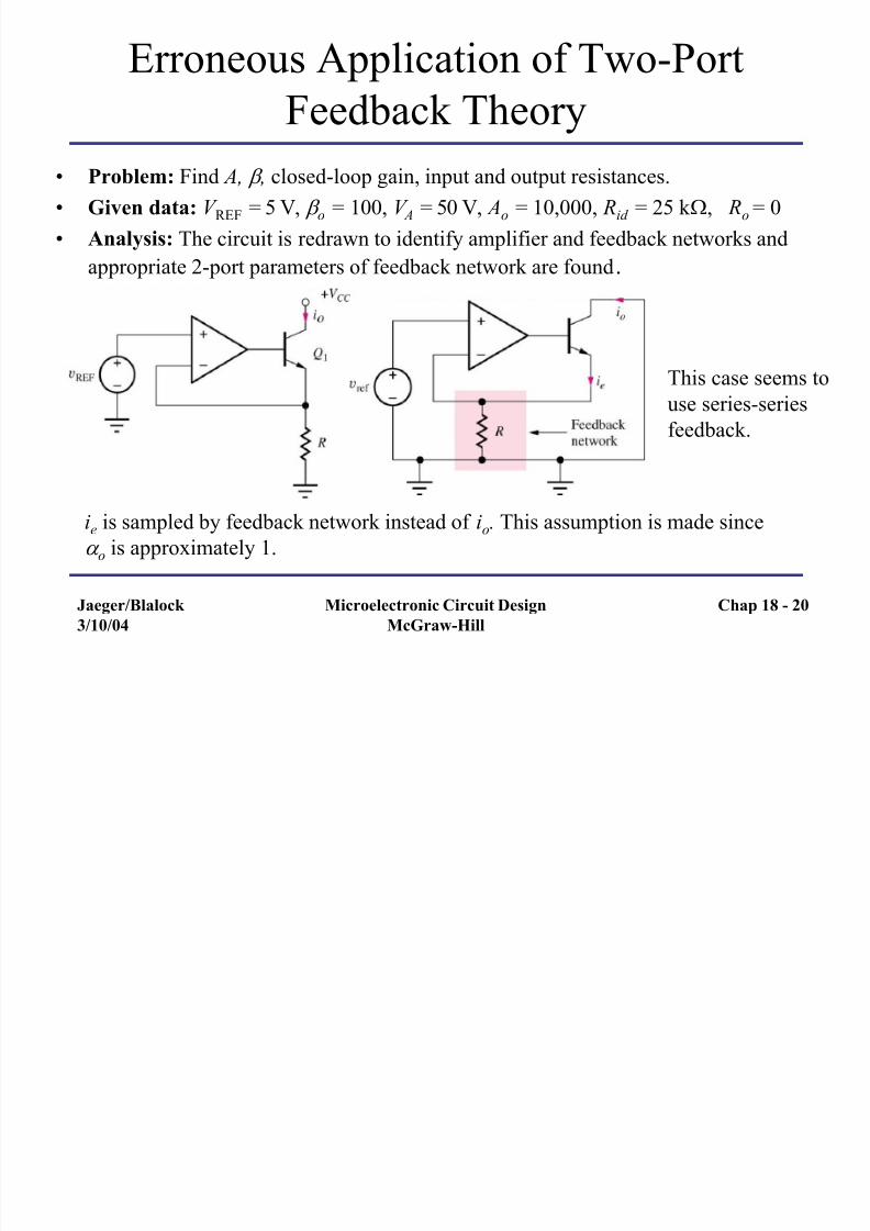
• Gain of amplifier should includeeffects of , , R I and R L.
• Required y-parameters are foundfrom their individual definitions.
• Two-port representation of theamplifier is as shown.
11 F z
22 F z
7/27/2019 Chap18-Feedback, Stability and Oscillators
http://slidepdf.com/reader/full/chap18-feedback-stability-and-oscillators 20/58
7/27/2019 Chap18-Feedback, Stability and Oscillators
http://slidepdf.com/reader/full/chap18-feedback-stability-and-oscillators 21/58
Jaeger/Blalock 3/10/04
Microelectronic Circuit DesignMcGraw-Hill
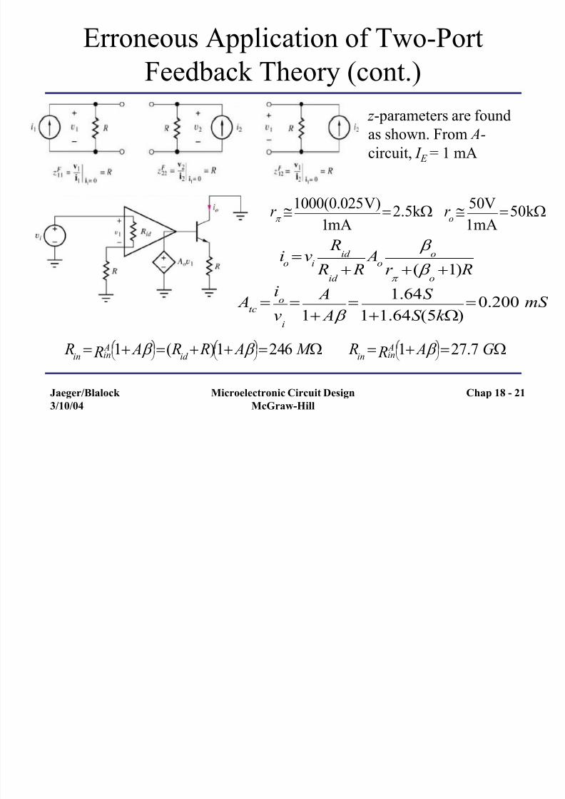
Erroneous Application of Two-Port
Feedback Theory (cont.)
z -parameters are found
as shown. From A-
circuit, I E = 1 mA
r
1000(0.025V)
1mA2.5k W r
o 50V
1mA50k W
iovi
Rid
Rid R Ao
b o
r ( b o1) R
Atc io
vi
A1 A b
1.64S 11.64S (5k W)
0.200 mS
Rin
in A R 1 A b
( R
id R)1 A b
246 M W R
in in
A R 1 A b
27.7 GW
Chap 18 - 21
7/27/2019 Chap18-Feedback, Stability and Oscillators
http://slidepdf.com/reader/full/chap18-feedback-stability-and-oscillators 22/58
Jaeger/Blalock 3/10/04
Microelectronic Circuit DesignMcGraw-Hill
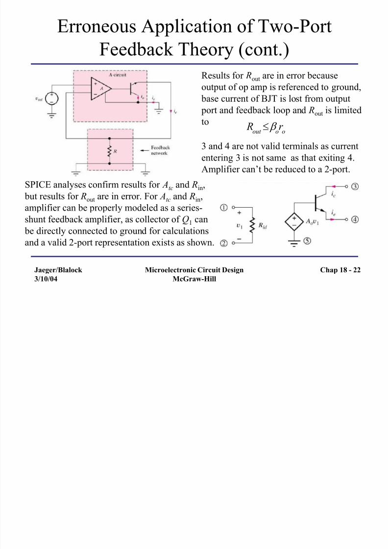
Erroneous Application of Two-Port
Feedback Theory (cont.)
SPICE analyses confirm results for Atc and Rin,
but results for Rout are in error. For Atc and Rin,
amplifier can be properly modeled as a series-
shunt feedback amplifier, as collector of Q1 can
be directly connected to ground for calculations
and a valid 2-port representation exists as shown.
Results for Rout are in error because
output of op amp is referenced to ground,
base current of BJT is lost from output
port and feedback loop and Rout is limited
to
3 and 4 are not valid terminals as current
entering 3 is not same as that exiting 4.
Amplifier can’t be reduced to a 2-port.
Rout
b or
o
Chap 18 - 22
7/27/2019 Chap18-Feedback, Stability and Oscillators
http://slidepdf.com/reader/full/chap18-feedback-stability-and-oscillators 23/58
Jaeger/Blalock 3/10/04
Microelectronic Circuit DesignMcGraw-Hill
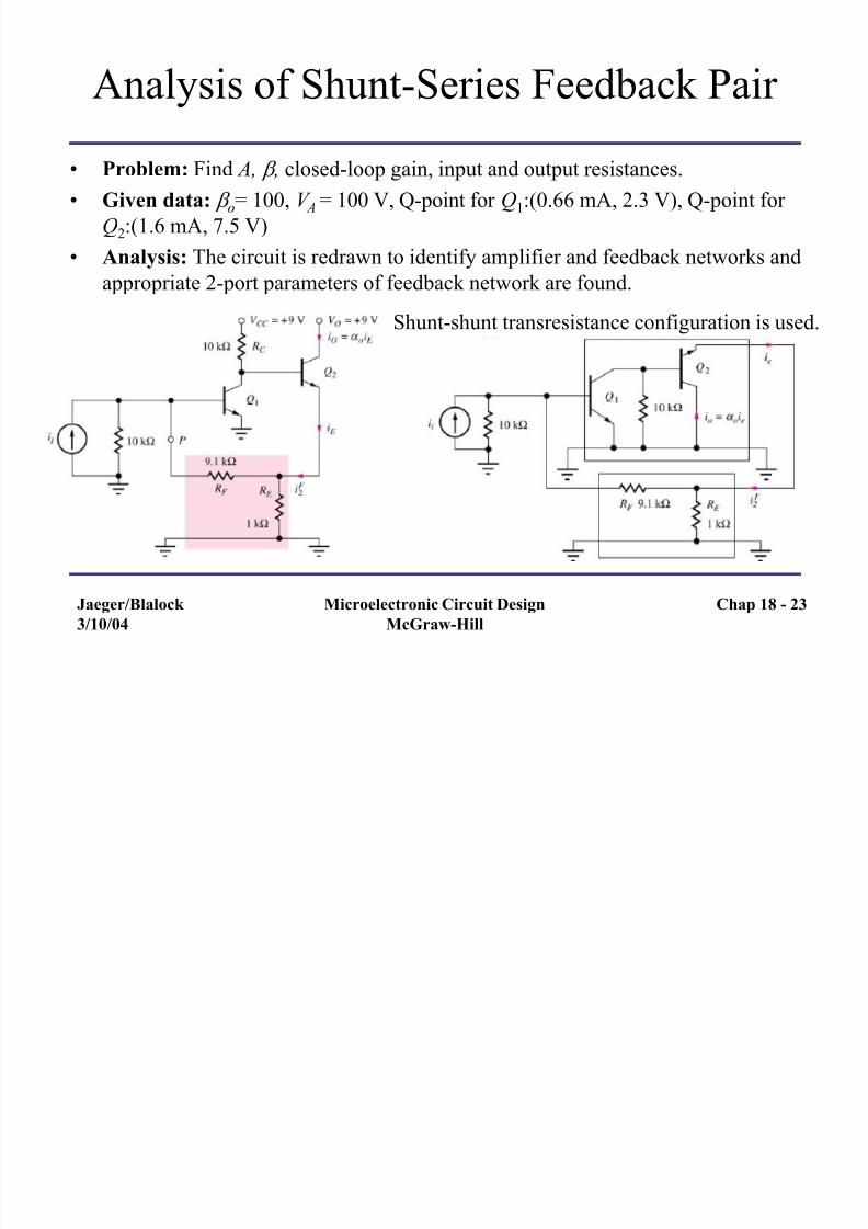
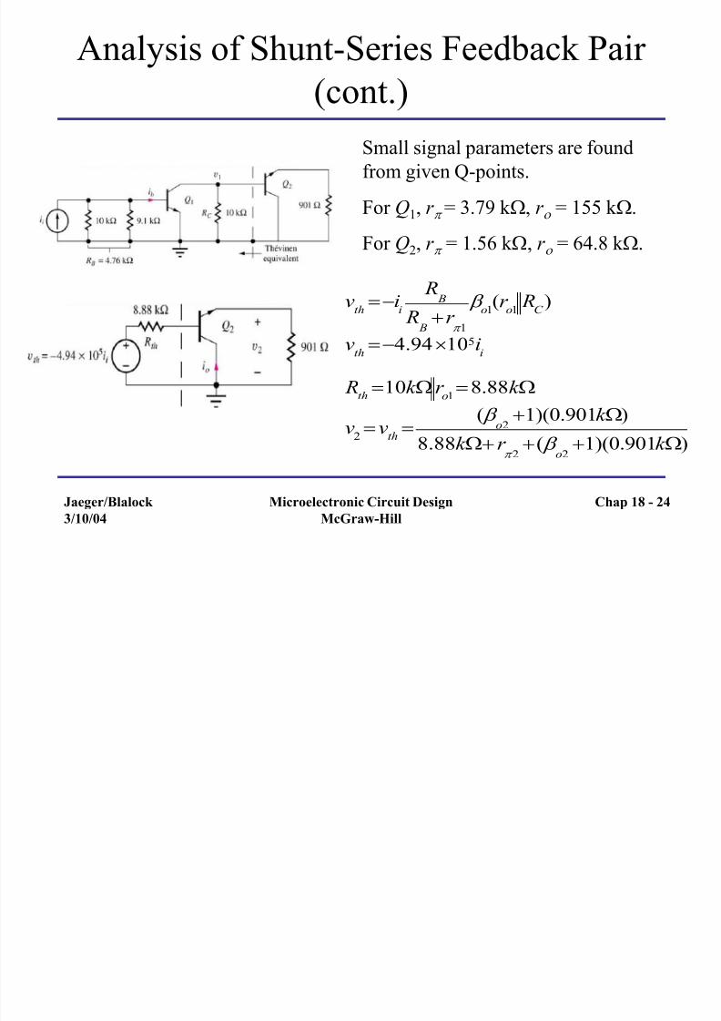
Analysis of Shunt-Series Feedback Pair
• Problem: Find A, b , closed-loop gain, input and output resistances.
• Given data: b o= 100, V A = 100 V, Q-point for Q1:(0.66 mA, 2.3 V), Q-point for
Q2:(1.6 mA, 7.5 V)
• Analysis: The circuit is redrawn to identify amplifier and feedback networks and
appropriate 2-port parameters of feedback network are found.
Shunt-shunt transresistance configuration is used.
Chap 18 - 23
7/27/2019 Chap18-Feedback, Stability and Oscillators
http://slidepdf.com/reader/full/chap18-feedback-stability-and-oscillators 24/58
Jaeger/Blalock 3/10/04
Microelectronic Circuit DesignMcGraw-Hill
Analysis of Shunt-Series Feedback Pair
(cont.)
Small signal parameters are found
from given Q-points.
For Q1, r = 3.79 k W, r o = 155 k W.
For Q2, r
= 1.56 k W, r
o = 64.8 k W.
vthii
R B
R Br
1
b o1
(r o1 RC )
vth4.94105i
i
Rth 10k W r o18.88k W
v2vth
( b o21)(0.901k W)
8.88k W r 2( b o21)(0.901k W)
Chap 18 - 24
7/27/2019 Chap18-Feedback, Stability and Oscillators
http://slidepdf.com/reader/full/chap18-feedback-stability-and-oscillators 25/58
Jaeger/Blalock 3/10/04
Microelectronic Circuit DesignMcGraw-Hill
Analysis of Shunt-Series Feedback Pair
(cont.)
Av
2
ii
4.43105 W
b 12
F y 1
9100S
Atr
A
1 A b 8910 W
Rin
in
A R
(1 A b )
R B
r 1
(1 A b ) 42.5 W
Rout
out A R
(1 A b )1.86 W
Closed-loop current gain is given by:
Ai
io
ii
a
oi
e
ii
a o
v2
901Wi
i
a
o
901W A
tr 9.79
Chap 18 - 25
7/27/2019 Chap18-Feedback, Stability and Oscillators
http://slidepdf.com/reader/full/chap18-feedback-stability-and-oscillators 26/58
Jaeger/Blalock 3/10/04
Microelectronic Circuit DesignMcGraw-Hill
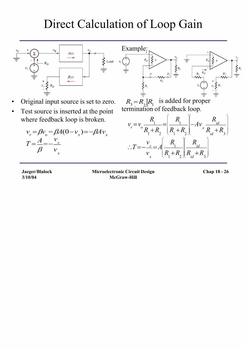
Direct Calculation of Loop Gain
• Original input source is set to zero.
• Test source is inserted at the point
where feedback loop is broken.
vr b vo b A(0v x) b Av x
T A
b vr
v x
Example:
is added for proper
termination of feedback loop.
R3 R
2 R
1
vr v
o
R1
R1 R2
R
1
R1 R2
Av x
Rid
Rid R3
T v
r
v x
A R
1
R1 R
2
Rid
Rid
R3
Chap 18 - 26
7/27/2019 Chap18-Feedback, Stability and Oscillators
http://slidepdf.com/reader/full/chap18-feedback-stability-and-oscillators 27/58
Jaeger/Blalock 3/10/04
Microelectronic Circuit DesignMcGraw-Hill
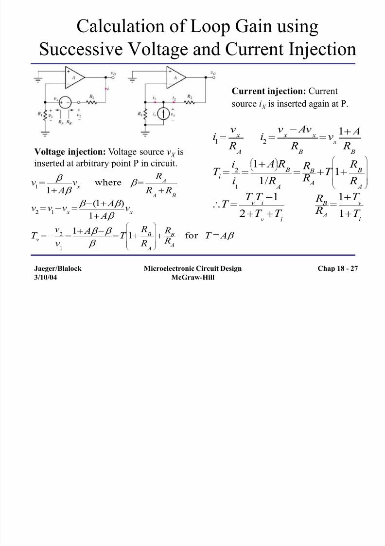
Calculation of Loop Gain using
Successive Voltage and Current Injection
Voltage injection: Voltage source v X is
inserted at arbitrary point P in circuit.
v1
b
1 A b v x
where b R A
R A R B
v2v1v x b (1 A b )
1 A b v x
T vv
2
v1
1 A b b
b T 1 R B
R A
R B
R A
for T = A b
Current injection: Current
source i X is inserted again at P.
i1
v x
R A
i2
v x
Av x
R B
v x1 A R B
T ii2
i1
1 A
R B
1/ R A
R B
R A
T 1 R B
R A
T
T v
T i
1
2T vT i
R B R A
1T v
1T i
Chap 18 - 27
7/27/2019 Chap18-Feedback, Stability and Oscillators
http://slidepdf.com/reader/full/chap18-feedback-stability-and-oscillators 28/58
Jaeger/Blalock 3/10/04
Microelectronic Circuit DesignMcGraw-Hill
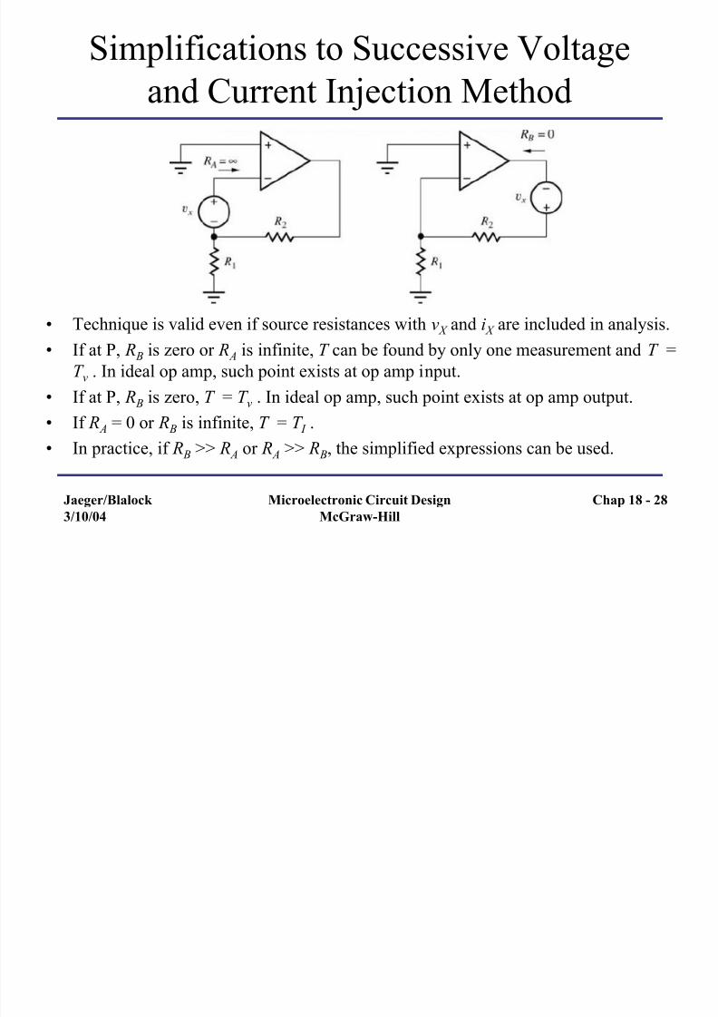
Simplifications to Successive Voltage
and Current Injection Method
• Technique is valid even if source resistances with v X and i X are included in analysis.
• If at P, R B is zero or R A is infinite, T can be found by only one measurement and T =
T v . In ideal op amp, such point exists at op amp input.• If at P, R B is zero, T = T v . In ideal op amp, such point exists at op amp output.
• If R A = 0 or R B is infinite, T = T I .
• In practice, if R B >> R A or R A >> R B, the simplified expressions can be used.
Chap 18 - 28
7/27/2019 Chap18-Feedback, Stability and Oscillators
http://slidepdf.com/reader/full/chap18-feedback-stability-and-oscillators 29/58
Jaeger/Blalock 3/10/04
Microelectronic Circuit DesignMcGraw-Hill
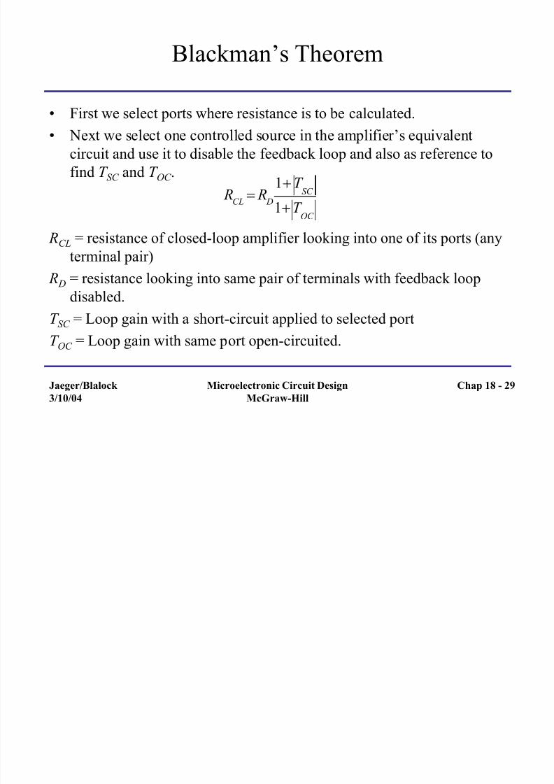
Blackman’s Theorem
• First we select ports where resistance is to be calculated.
• Next we select one controlled source in the amplifier’s equivalent
circuit and use it to disable the feedback loop and also as reference to
find T SC and T OC .
RCL = resistance of closed-loop amplifier looking into one of its ports (any
terminal pair)
R D = resistance looking into same pair of terminals with feedback loop
disabled.
T SC = Loop gain with a short-circuit applied to selected port
T OC = Loop gain with same port open-circuited.
RCL R D
1 T SC
1 T OC
Chap 18 - 29
7/27/2019 Chap18-Feedback, Stability and Oscillators
http://slidepdf.com/reader/full/chap18-feedback-stability-and-oscillators 30/58
Jaeger/Blalock 3/10/04
Microelectronic Circuit DesignMcGraw-Hill
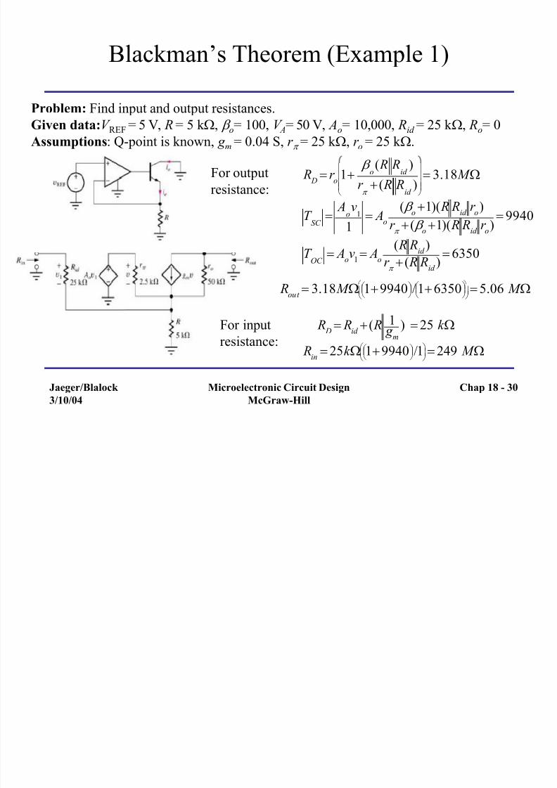
Blackman’s Theorem (Example 1)
For output
resistance:
R D
r o1
b o( R R
id )
r
( R Rid
)
3.18 M W
T SC
A
ov
1
1 A
o
( b o1)( R R
id r
o)
r
( b o1)( R R
id r
o)
9940
T OC
Aov
1 A
o
( R Rid
)
r
( R Rid
) 6350
Problem: Find input and output resistances.
Given data:V REF = 5 V, R = 5 k W, b o= 100, V A= 50 V, Ao= 10,000, Rid = 25 k W, Ro= 0
Assumptions: Q-point is known, g m = 0.04 S, r = 25 k W, r o = 25 k W.
Rout 3.18 M W 1 9940
/1 6350
5.06 M W
For input
resistance:
R D
Rid
( R 1 g
m
) 25 k W
Rin
25k W 1 9940
/1
249 M W
Chap 18 - 30
7/27/2019 Chap18-Feedback, Stability and Oscillators
http://slidepdf.com/reader/full/chap18-feedback-stability-and-oscillators 31/58
Jaeger/Blalock 3/10/04 Microelectronic Circuit DesignMcGraw-Hill
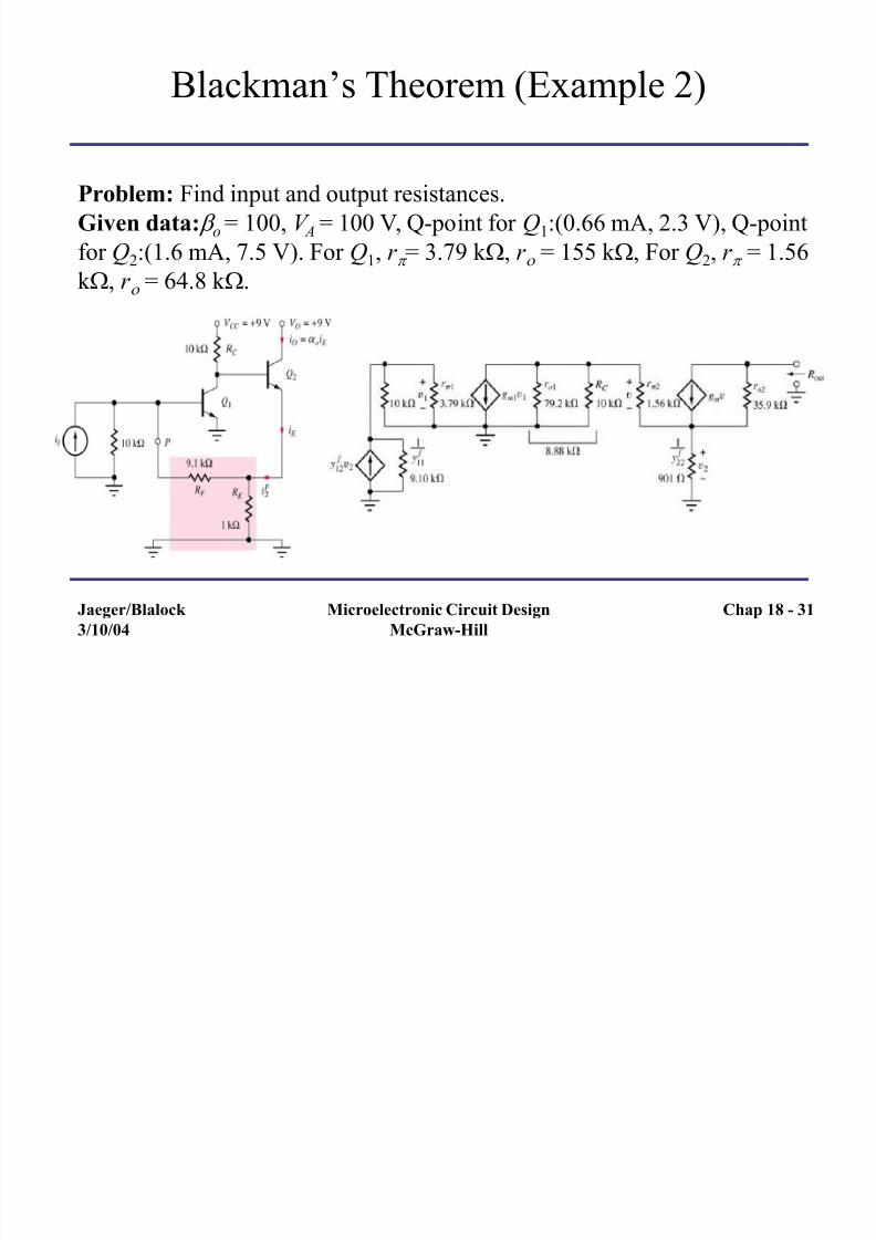
Blackman’s Theorem (Example 2)
Problem: Find input and output resistances.
Given data: b o = 100, V A = 100 V, Q-point for Q1:(0.66 mA, 2.3 V), Q-point
for Q2:(1.6 mA, 7.5 V). For Q1, r = 3.79 k W, r o = 155 k W, For Q2, r = 1.56
k W, r o = 64.8 k W.
Chap 18 - 31
7/27/2019 Chap18-Feedback, Stability and Oscillators
http://slidepdf.com/reader/full/chap18-feedback-stability-and-oscillators 32/58
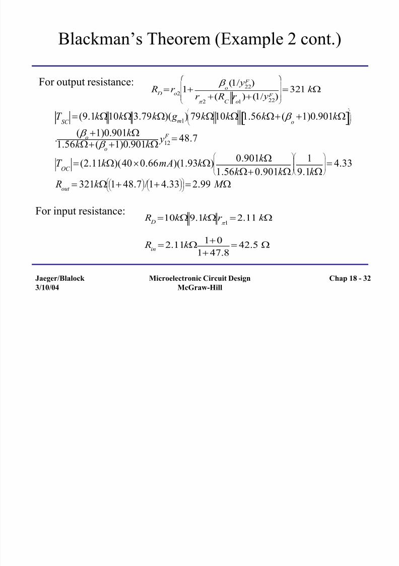
Jaeger/Blalock 3/10/04 Microelectronic Circuit DesignMcGraw-Hill
Blackman’s Theorem (Example 2 cont.)
R Dr o2
1b o(1/
22 F y )
r 2( RC r o1
)(1/22 F y )
321 k W
T SC
(9.1k W10k W 3.79k W)( g m1
) 79k W 10k W 1.56k W ( b o
1)0.901k W
.
( b o1)0.901k W
1.56k W( b o 1)0.901k W 12
F
y 48.7
T OC
(2.11k W)(400.66mA)(1.93k W)0.901k W
1.56k W 0.901k W
1
9.1k W
4.33
Rout
321k W 1 48.7
/1 4.33
2.99 M W
For input resistance:
R D10k W9.1k W r
12.11 k W
Rin2.11k W 10
147.8 42.5 W
For output resistance:
Chap 18 - 32
7/27/2019 Chap18-Feedback, Stability and Oscillators
http://slidepdf.com/reader/full/chap18-feedback-stability-and-oscillators 33/58
Jaeger/Blalock 3/10/04 Microelectronic Circuit DesignMcGraw-Hill
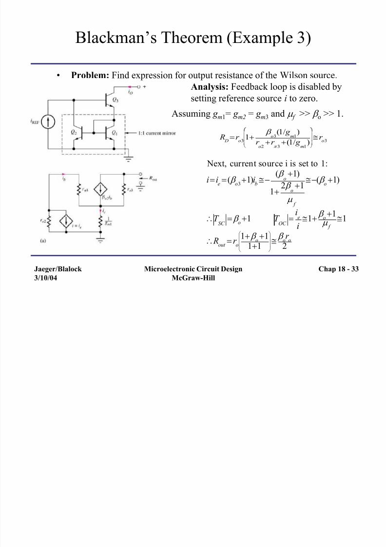
Blackman’s Theorem (Example 3)
• Problem: Find expression for output resistance of the Wilson source.
Analysis: Feedback loop is disabled by
setting reference source i to zero.
R Dr o3 1
b o3
(1/ g m1
)
r o2r
3(1/ g
m1)
r o3
Assuming g m1= g m2 = g m3 and m f >> b o >> 1.
Next, current source i is set to 1:
i ie ( b
o31)i
b
( b o
1)
12 b
o1
m f
( b o1)
T SC
b o1 T
OC
ie
i1 b o 1
m f
1
Rout
r o
1 b o1
11
b
or
o
2
Chap 18 - 33
7/27/2019 Chap18-Feedback, Stability and Oscillators
http://slidepdf.com/reader/full/chap18-feedback-stability-and-oscillators 34/58
Jaeger/Blalock 3/10/04 Microelectronic Circuit DesignMcGraw-Hill
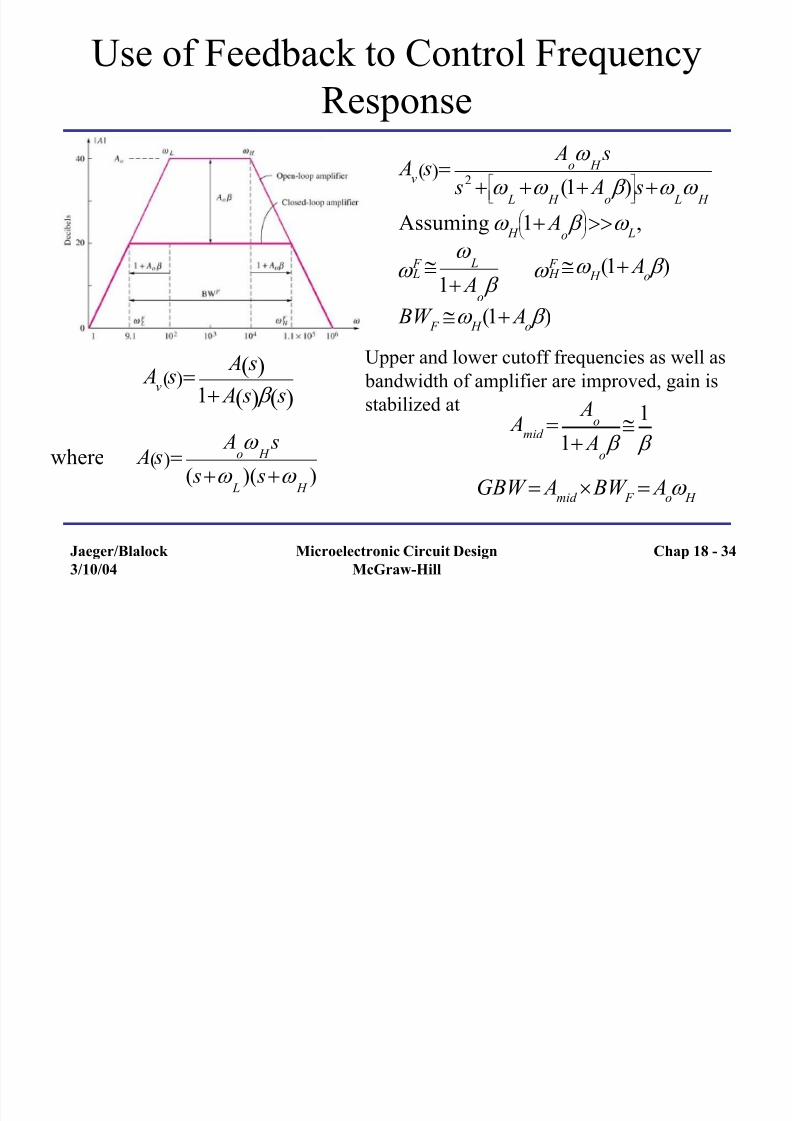
Use of Feedback to Control Frequency
Response
Av
s A s
1 A s b s
A s A
o
H s
( s L
)( s H
)where
Av
s A
o
H s
s2 L
H
(1 Ao b )
s
L
H
Assuming H
1 Ao b
L,
L F
L
1 Ao b H
F
H
(1 Ao
b )
BW F
H
(1 Ao b )
Upper and lower cutoff frequencies as well as
bandwidth of amplifier are improved, gain is
stabilized at
Amid Ao
1 Ao b
1 b
GBW Amid
BW F
Ao
H
Chap 18 - 34
7/27/2019 Chap18-Feedback, Stability and Oscillators
http://slidepdf.com/reader/full/chap18-feedback-stability-and-oscillators 35/58
Jaeger/Blalock 3/10/04 Microelectronic Circuit DesignMcGraw-Hill
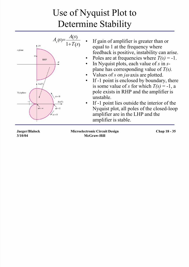
Use of Nyquist Plot to
Determine Stability
• If gain of amplifier is greater than or equal to 1 at the frequency wherefeedback is positive, instability can arise.
• Poles are at frequencies where T(s) = -1.• In Nyquist plots, each value of s in s-
plane has corresponding value of T(s).• Values of s on j axis are plotted.• If -1 point is enclosed by boundary, there
is some value of s for which T(s) = -1, a pole exists in RHP and the amplifier is
unstable.• If -1 point lies outside the interior of the Nyquist plot, all poles of the closed-loopamplifier are in the LHP and theamplifier is stable.
Av
s A s
1T s
Chap 18 - 35
7/27/2019 Chap18-Feedback, Stability and Oscillators
http://slidepdf.com/reader/full/chap18-feedback-stability-and-oscillators 36/58
Jaeger/Blalock 3/10/04 Microelectronic Circuit DesignMcGraw-Hill
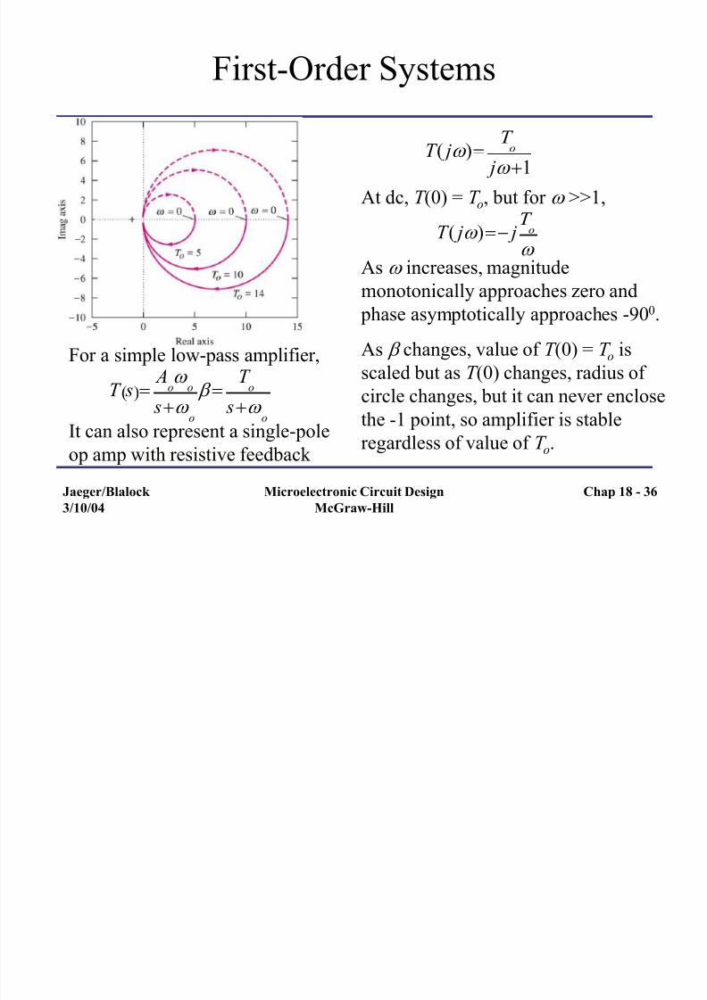
First-Order Systems
For a simple low-pass amplifier,
It can also represent a single-pole
op amp with resistive feedback
T s Ao o s
o
b T o s
o
T ( j )T o
j 1
At dc, T (0) = T o, but for >>1,
As increases, magnitude
monotonically approaches zero and
phase asymptotically approaches -900.
As b changes, value of T (0) = T o is
scaled but as T (0) changes, radius of circle changes, but it can never enclose
the -1 point, so amplifier is stable
regardless of value of T o.
T ( j ) jT o
Chap 18 - 36
7/27/2019 Chap18-Feedback, Stability and Oscillators
http://slidepdf.com/reader/full/chap18-feedback-stability-and-oscillators 37/58
Jaeger/Blalock 3/10/04 Microelectronic Circuit DesignMcGraw-Hill
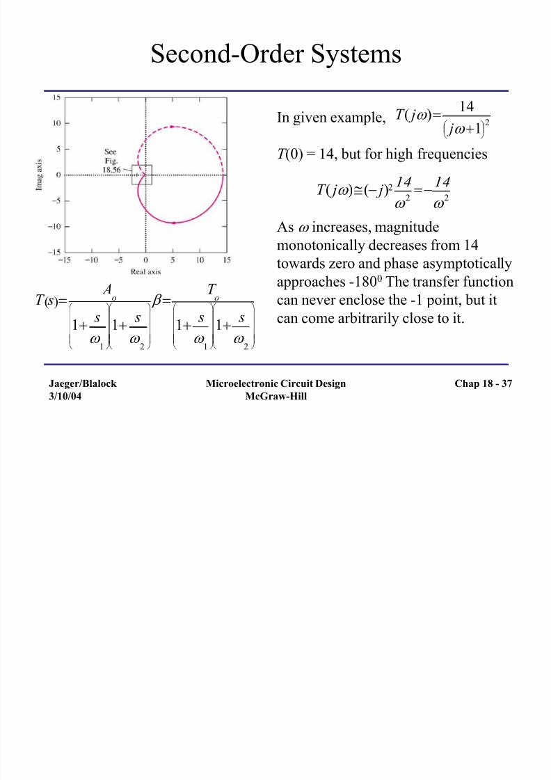
Second-Order Systems
T s Ao
1 s
1
1 s
2
b T o
1 s
1
1 s
2
In given example,
T (0) = 14, but for high frequencies
As increases, magnitude
monotonically decreases from 14
towards zero and phase asymptotically
approaches -1800 The transfer function
can never enclose the -1 point, but it
can come arbitrarily close to it.
T ( j ) 14
j 1
2
T ( j )( j)2 14
2
14
2
Chap 18 - 37
7/27/2019 Chap18-Feedback, Stability and Oscillators
http://slidepdf.com/reader/full/chap18-feedback-stability-and-oscillators 38/58
Jaeger/Blalock 3/10/04 Microelectronic Circuit DesignMcGraw-Hill
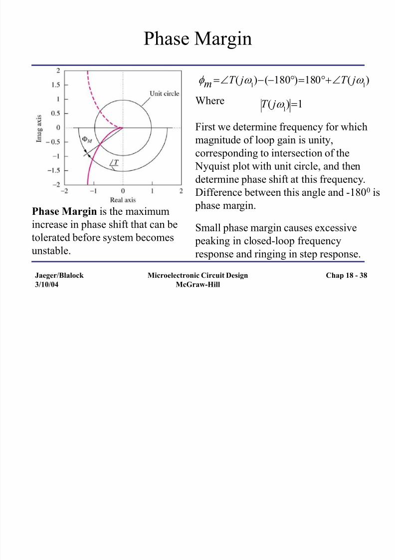
Phase Margin
Phase Margin is the maximumincrease in phase shift that can be
tolerated before system becomes
unstable.
m T ( j 1)(180)180T ( j
1)
Where
First we determine frequency for which
magnitude of loop gain is unity,corresponding to intersection of the
Nyquist plot with unit circle, and then
determine phase shift at this frequency.
Difference between this angle and -1800 is
phase margin.
Small phase margin causes excessive
peaking in closed-loop frequency
response and ringing in step response.
T ( j 1) 1
Chap 18 - 38
7/27/2019 Chap18-Feedback, Stability and Oscillators
http://slidepdf.com/reader/full/chap18-feedback-stability-and-oscillators 39/58
Jaeger/Blalock 3/10/04 Microelectronic Circuit DesignMcGraw-Hill
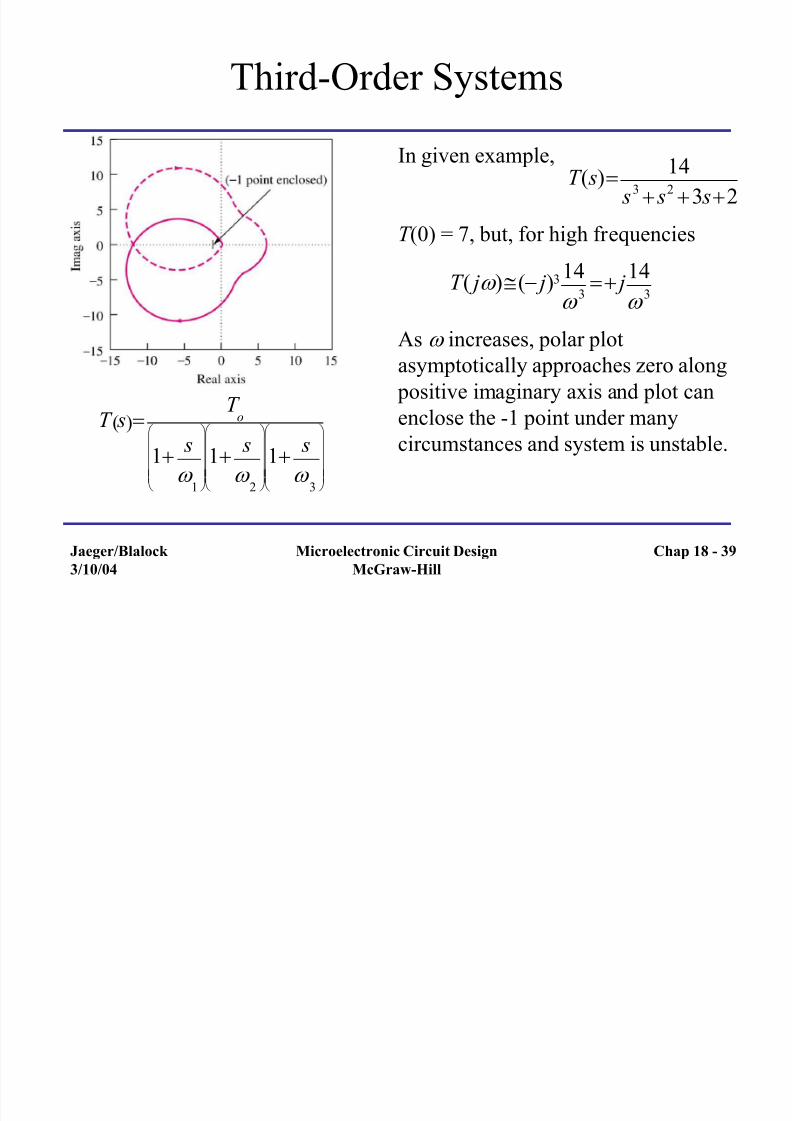
Third-Order Systems
In given example,
T (0) = 7, but, for high frequencies
As increases, polar plot
asymptotically approaches zero along
positive imaginary axis and plot can
enclose the -1 point under manycircumstances and system is unstable.
T s T
o
1 s
1
1 s
2
1 s
3
T ( s) 14
s3 s2 3 s2
T ( j )( j)3 14 3 j14
3
Chap 18 - 39
7/27/2019 Chap18-Feedback, Stability and Oscillators
http://slidepdf.com/reader/full/chap18-feedback-stability-and-oscillators 40/58
Jaeger/Blalock 3/10/04 Microelectronic Circuit DesignMcGraw-Hill
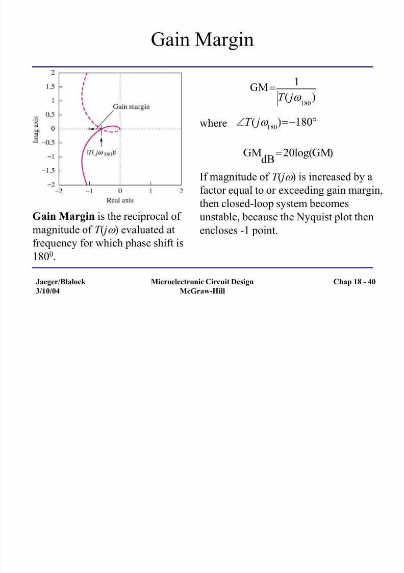
Gain Margin
Gain Margin is the reciprocal of magnitude of T ( j ) evaluated at
frequency for which phase shift is
1800.
GM 1
T ( j 180
)
where
If magnitude of T ( j ) is increased by a
factor equal to or exceeding gain margin,
then closed-loop system becomes
unstable, because the Nyquist plot thenencloses -1 point.
T ( j 180
)180
GM)log(20dB
GM
Chap 18 - 40
7/27/2019 Chap18-Feedback, Stability and Oscillators
http://slidepdf.com/reader/full/chap18-feedback-stability-and-oscillators 41/58
Jaeger/Blalock 3/10/04 Microelectronic Circuit DesignMcGraw-Hill
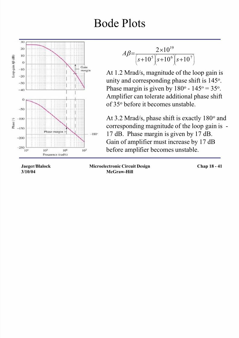
Bode Plots
A b 21019
s105
s106
s107
At 1.2 Mrad/s, magnitude of the loop gain is
unity and corresponding phase shift is 145o.
Phase margin is given by 180o - 145o = 35o.
Amplifier can tolerate additional phase shift
of 35o before it becomes unstable.
At 3.2 Mrad/s, phase shift is exactly 180o and
corresponding magnitude of the loop gain is -17 dB. Phase margin is given by 17 dB.
Gain of amplifier must increase by 17 dB
before amplifier becomes unstable.
Chap 18 - 41
7/27/2019 Chap18-Feedback, Stability and Oscillators
http://slidepdf.com/reader/full/chap18-feedback-stability-and-oscillators 42/58
Jaeger/Blalock 3/10/04 Microelectronic Circuit DesignMcGraw-Hill
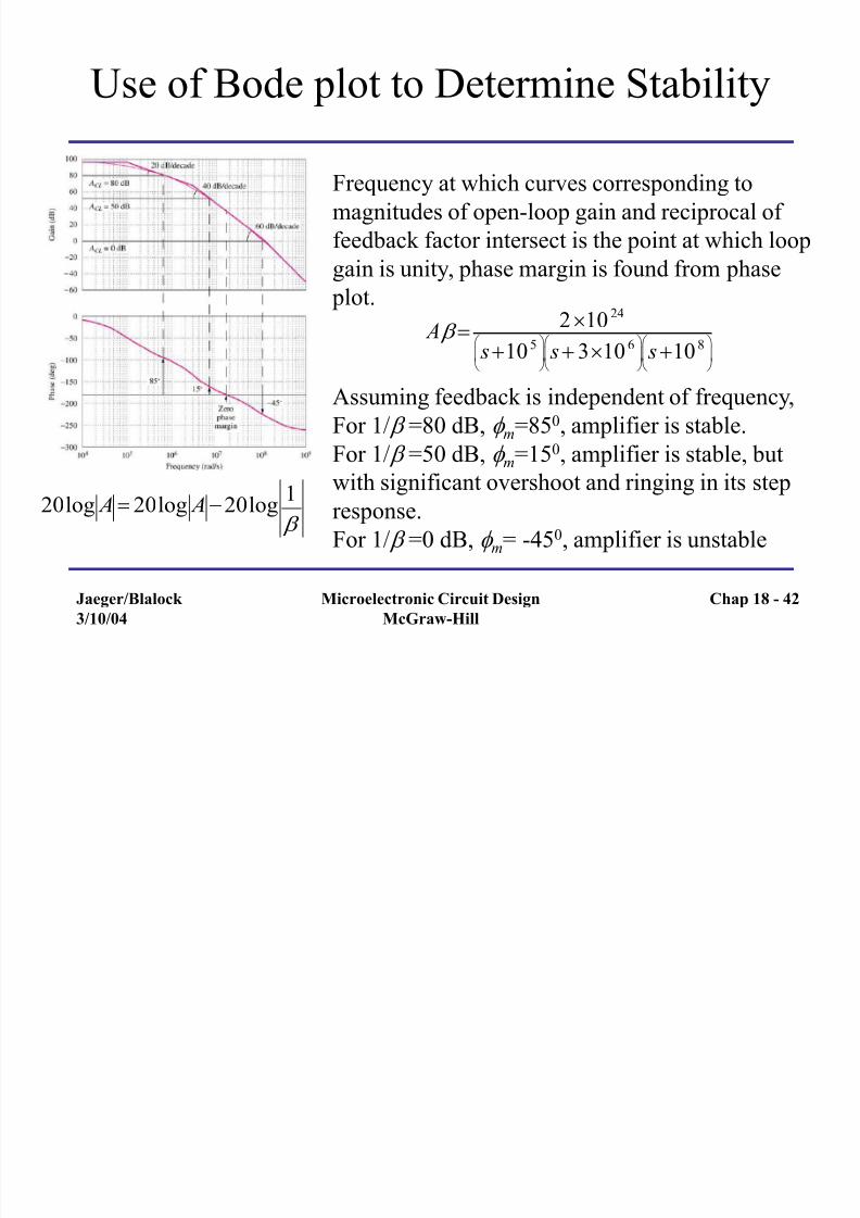
Use of Bode plot to Determine Stability
b
1log20log20log20 A A
Frequency at which curves corresponding to
magnitudes of open-loop gain and reciprocal of
feedback factor intersect is the point at which loop
gain is unity, phase margin is found from phase
plot.
Assuming feedback is independent of frequency,
For 1/ b =80 dB, m=850, amplifier is stable.
For 1/ b =50 dB, m=150, amplifier is stable, butwith significant overshoot and ringing in its step
response.
For 1/ b =0 dB, m= -450, amplifier is unstable
A b 210 24
s 10 5
s 310 6
s 10 8
Chap 18 - 42
7/27/2019 Chap18-Feedback, Stability and Oscillators
http://slidepdf.com/reader/full/chap18-feedback-stability-and-oscillators 43/58
Jaeger/Blalock 3/10/04 Microelectronic Circuit DesignMcGraw-Hill
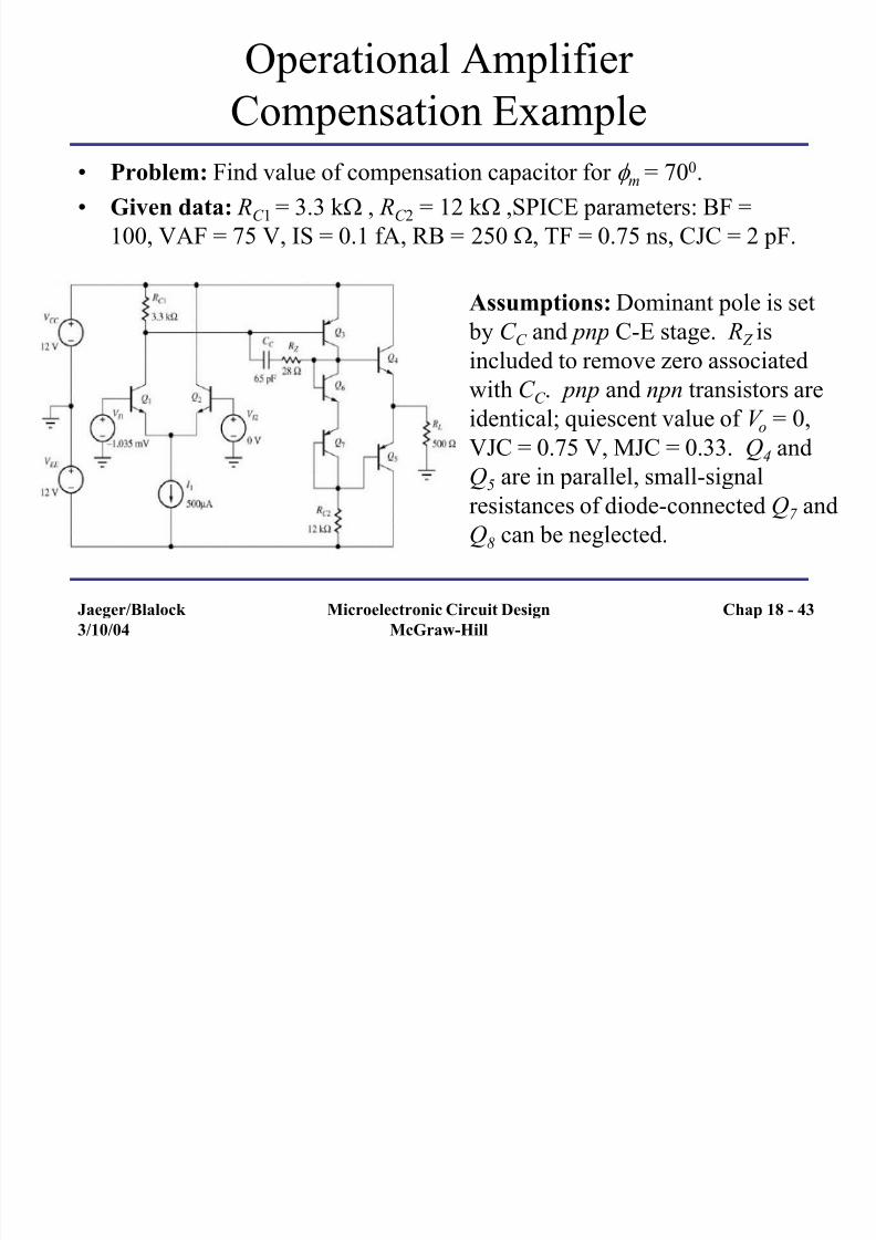
Operational Amplifier
Compensation Example
• Problem: Find value of compensation capacitor for m = 700.
• Given data: RC 1 = 3.3 k W , RC 2 = 12 k W ,SPICE parameters: BF =
100, VAF = 75 V, IS = 0.1 fA, RB = 250 W, TF = 0.75 ns, CJC = 2 pF.
Assumptions: Dominant pole is set by C C and pnp C-E stage. R Z is
included to remove zero associated
with C C . pnp and npn transistors are
identical; quiescent value of V o = 0,
VJC = 0.75 V, MJC = 0.33. Q4 and
Q5 are in parallel, small-signal
resistances of diode-connected Q7 and
Q8 can be neglected.
Chap 18 - 43
7/27/2019 Chap18-Feedback, Stability and Oscillators
http://slidepdf.com/reader/full/chap18-feedback-stability-and-oscillators 44/58
Jaeger/Blalock
3/10/04
Microelectronic Circuit Design
McGraw-Hill
Operational Amplifier
Compensation Example (cont.)
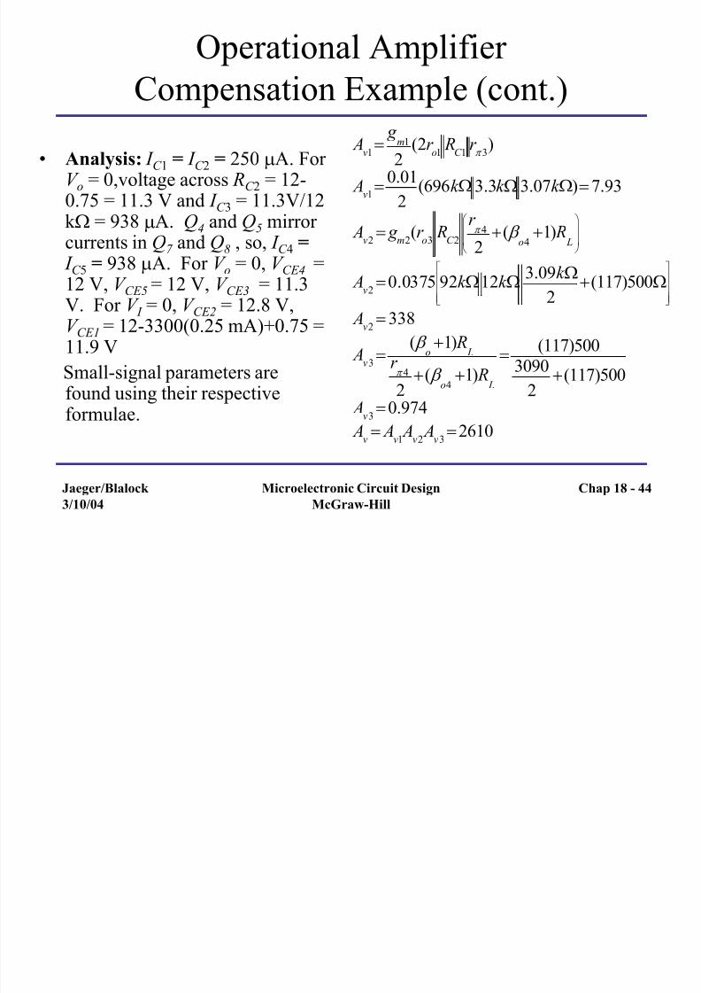
• Analysis: I C 1 = I C 2 = 250 mA. For V o = 0,voltage across RC 2 = 12-0.75 = 11.3 V and I C 3 = 11.3V/12k W= 938 mA. Q4 and Q5 mirror
currents in Q7 and Q8 , so, I C 4 = I C 5 = 938 mA. For V o = 0, V CE4 =12 V, V CE5 = 12 V, V CE3 = 11.3V. For V I = 0, V CE2 = 12.8 V,V CE1 = 12-3300(0.25 mA)+0.75 =11.9 V
Small-signal parameters arefound using their respectiveformulae.
Av1
g m1
2(2r
o1 R
C 1r 3
)
Av1
0.01
2(696k W 3.3k W 3.07k W) 7.93
Av2
g m2
(r o3
RC 2
r 4
2
( b o4
1) R L
Av2
0.0375 92k W12k W 3.09k W2
(117)500W
Av2
338
Av3
( b
o1) R
L
r 4
2 ( b o4 1) R L
(117)500
30902 (117)500
Av3
0.974
Av A
v1 A
v2 A
v3 2610
Chap 18 - 44
7/27/2019 Chap18-Feedback, Stability and Oscillators
http://slidepdf.com/reader/full/chap18-feedback-stability-and-oscillators 45/58
Jaeger/Blalock
3/10/04
Microelectronic Circuit Design
McGraw-Hill
Operational Amplifier
Compensation Example (cont.)
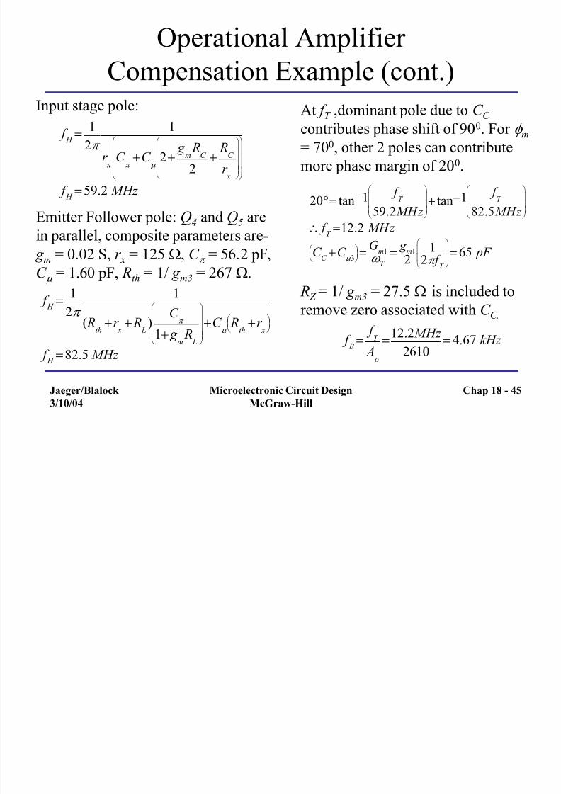
Input stage pole:
Emitter Follower pole: Q4 and Q5 are
in parallel, composite parameters are-
g m = 0.02 S, r x = 125 W, C = 56.2 pF,
C m = 1.60 pF, Rth = 1/ g m3 = 267 W.
f H
1
2
1
r
C
C m
2g
m R
C
2
RC
r x
f H
59.2 MHz
f H 12
1
( Rth
r x
R L
)C
1 g m R
L
C m
Rth
r x
f H
82.5 MHz
At f T ,dominant pole due to C C
contributes phase shift of 900. For m= 700, other 2 poles can contribute
more phase margin of 200.
20 tan1f
T
59.2 MHz
tan1
f T
82.5 MHz
f T
12.2 MHz
C C
C m 3
G
m1
T
g m1
21
2 f T
65 pF
R Z = 1/ g m3 = 27.5 W is included toremove zero associated with C C.
f B
f
T
Ao
12.2 MHz
2610 4.67 kHz
Chap 18 - 45
7/27/2019 Chap18-Feedback, Stability and Oscillators
http://slidepdf.com/reader/full/chap18-feedback-stability-and-oscillators 46/58
Jaeger/Blalock
3/10/04
Microelectronic Circuit Design
McGraw-Hill
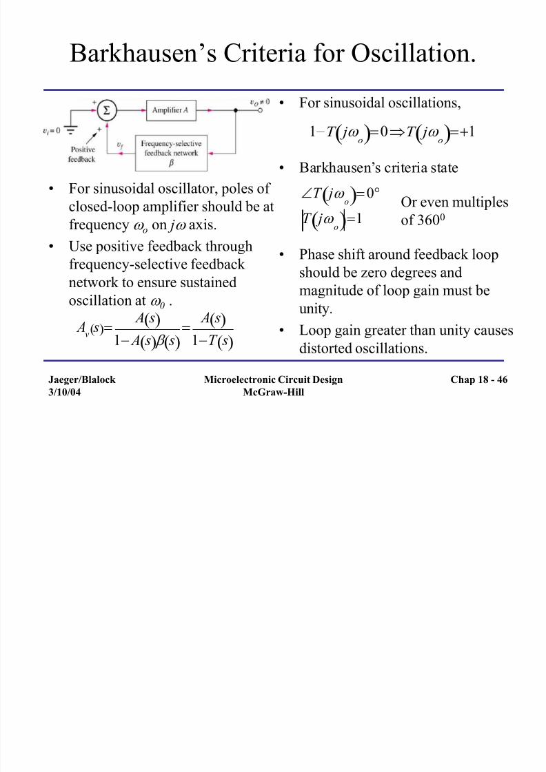
Barkhausen’s Criteria for Oscillation.
• For sinusoidal oscillator, poles of closed-loop amplifier should be at
frequency o on j axis.
• Use positive feedback through
frequency-selective feedback
network to ensure sustained
oscillation at 0 .
Av
s A s
1 A s b s
A s 1T s
• For sinusoidal oscillations,
• Barkhausen’s criteria state
• Phase shift around feedback loop
should be zero degrees and
magnitude of loop gain must beunity.
• Loop gain greater than unity causes
distorted oscillations.
1T j o 0T j
o 1
T j o 0
T j o 1
Or even multiples
of 3600
Chap 18 - 46
7/27/2019 Chap18-Feedback, Stability and Oscillators
http://slidepdf.com/reader/full/chap18-feedback-stability-and-oscillators 47/58
Jaeger/Blalock
3/10/04
Microelectronic Circuit Design
McGraw-Hill
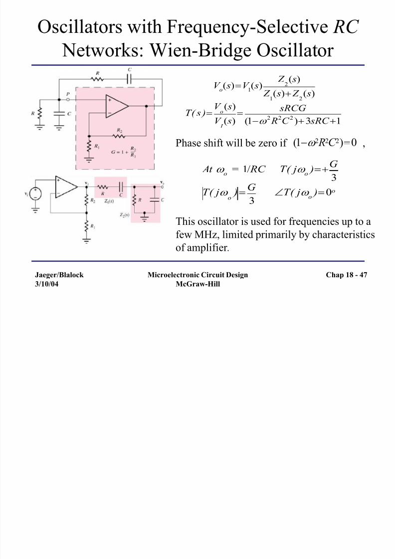
Oscillators with Frequency-Selective RC
Networks: Wien-Bridge Oscillator
V o( s)V
1( s) Z
2( s)
Z 1( s) Z
2( s)
T ( s )V o( s)
V I ( s)
sRCG
(1 2 R2C 2)3 sRC 1
Phase shift will be zero if ,
This oscillator is used for frequencies up to a
few MHz, limited primarily by characteristics
of amplifier .
(1 2 R2C 2)0
At o
= 1/ RC T ( j o )G
3
T ( j o )G
3 T ( j
o )0o
Chap 18 - 47
7/27/2019 Chap18-Feedback, Stability and Oscillators
http://slidepdf.com/reader/full/chap18-feedback-stability-and-oscillators 48/58
Jaeger/Blalock
3/10/04
Microelectronic Circuit Design
McGraw-Hill
Oscillators with Frequency-Selective RC
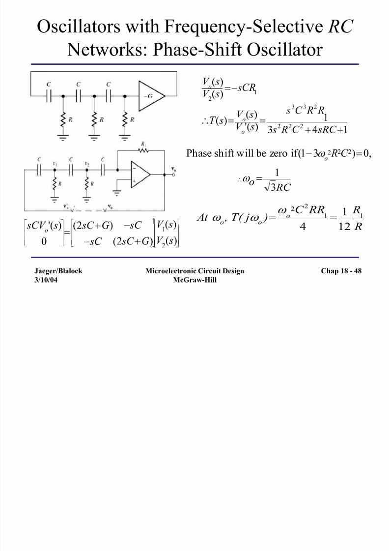
Networks: Phase-Shift Oscillator
sCV o'( s)
0
(2 sC G)
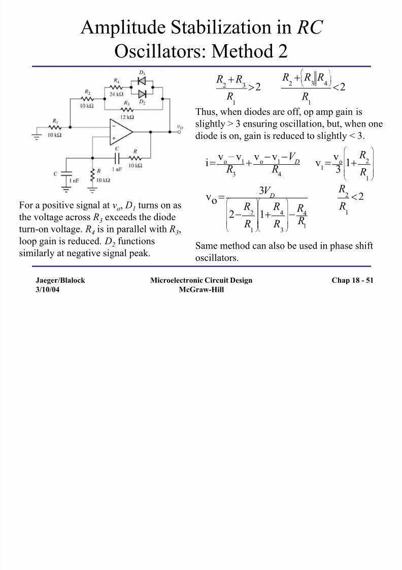
sC
sC
(2 sC G)
V 1( s)
V 2( s)
V o( s)
V 2( s)
sCR1
T ( s) V o( s)
V o'( s)
s3C 3 R2 R
13 s2 R2C 2 4 sRC 1
Phase shift will be zero if (1 3 o2 R2C 2) 0,
RC o
3
1
At o , T ( j
o )
o2C 2 RR1
4
1
12
R1 R
Chap 18 - 48
7/27/2019 Chap18-Feedback, Stability and Oscillators
http://slidepdf.com/reader/full/chap18-feedback-stability-and-oscillators 49/58
Jaeger/Blalock
3/10/04
Microelectronic Circuit Design
McGraw-Hill
Amplitude Stabilization
• Loop gain of oscillator changes due to power supply voltage,component value or temperature changes.
• If loop gain is too small, desired oscillation decays, and if it is toolarge, waveform is distorted.
• Amplitude stabilization or gain control is used to automaticallycontrol loop gain and place poles exactly on j axis.
• At power on, loop gain is larger than that required for oscillation.As oscillation builds up, gain is reduced o minimum required tosustain oscillations.
Chap 18 - 49
7/27/2019 Chap18-Feedback, Stability and Oscillators
http://slidepdf.com/reader/full/chap18-feedback-stability-and-oscillators 50/58
Jaeger/Blalock
3/10/04
Microelectronic Circuit Design
McGraw-Hill
Amplitude Stabilization in RC
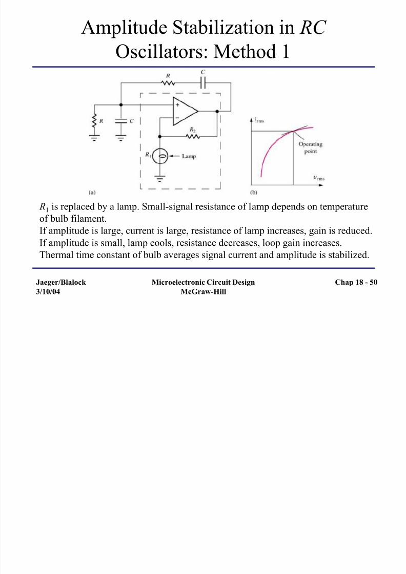
Oscillators: Method 1
R1 is replaced by a lamp. Small-signal resistance of lamp depends on temperature
of bulb filament.If amplitude is large, current is large, resistance of lamp increases, gain is reduced.
If amplitude is small, lamp cools, resistance decreases, loop gain increases.
Thermal time constant of bulb averages signal current and amplitude is stabilized.
Chap 18 - 50
7/27/2019 Chap18-Feedback, Stability and Oscillators
http://slidepdf.com/reader/full/chap18-feedback-stability-and-oscillators 51/58
7/27/2019 Chap18-Feedback, Stability and Oscillators
http://slidepdf.com/reader/full/chap18-feedback-stability-and-oscillators 52/58
Jaeger/Blalock
3/10/04
Microelectronic Circuit Design
McGraw-Hill
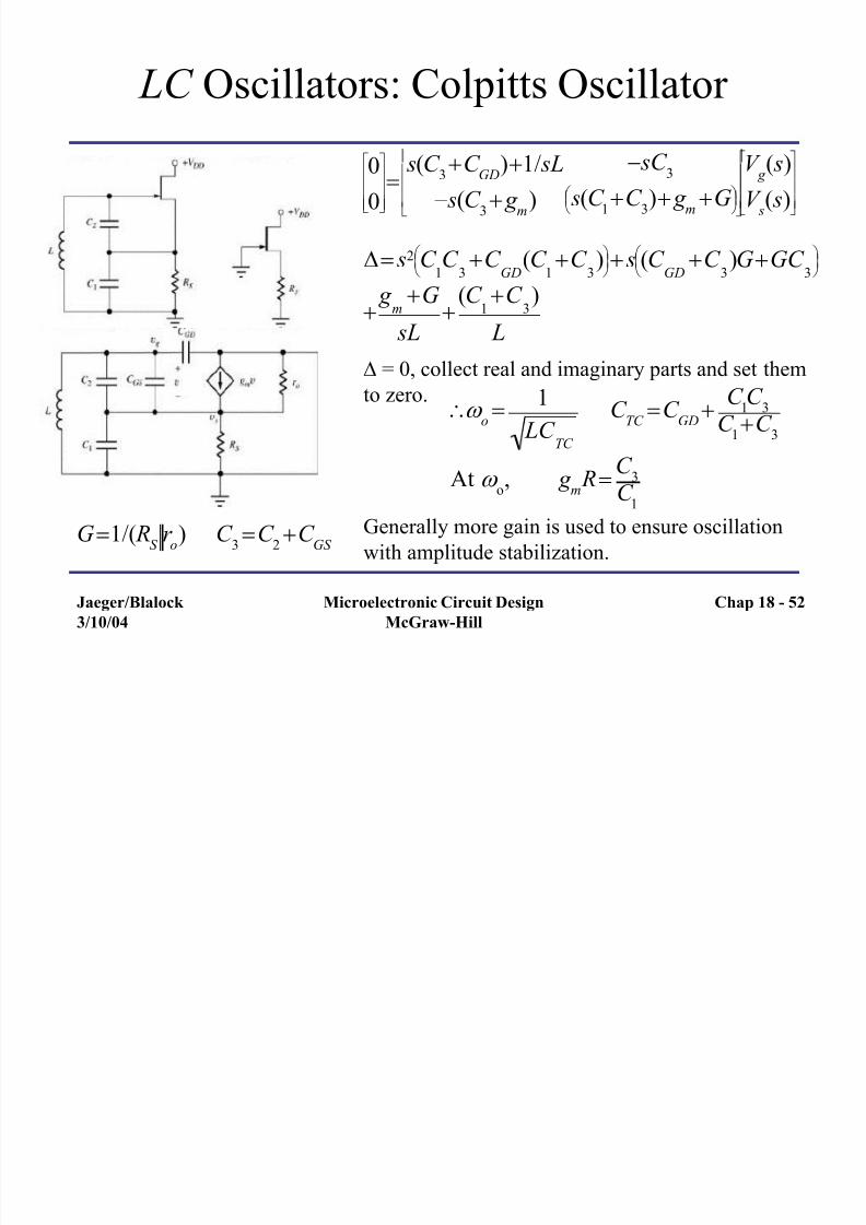
LC Oscillators: Colpitts Oscillator
G1/( RS
r o) C
3C
2C
GS
0
0
s(C 3 C GD)1/ sL
s(C 3 g
m)
sC 3
s(C 1C
3) g
mG
V g ( s)
V s( s)
s2 C 1C
3C
GD(C
1C
3)
s (C
GDC
3)GGC
3
g
m
G
sL (C
1
C 3
)
L
= 0, collect real and imaginary parts and set them
to zero.
o 1
LC TC
C TC
C GD
C 1C
3
C 1C
3
At o, g
m R C 3
C 1
Generally more gain is used to ensure oscillation
with amplitude stabilization.
Chap 18 - 52
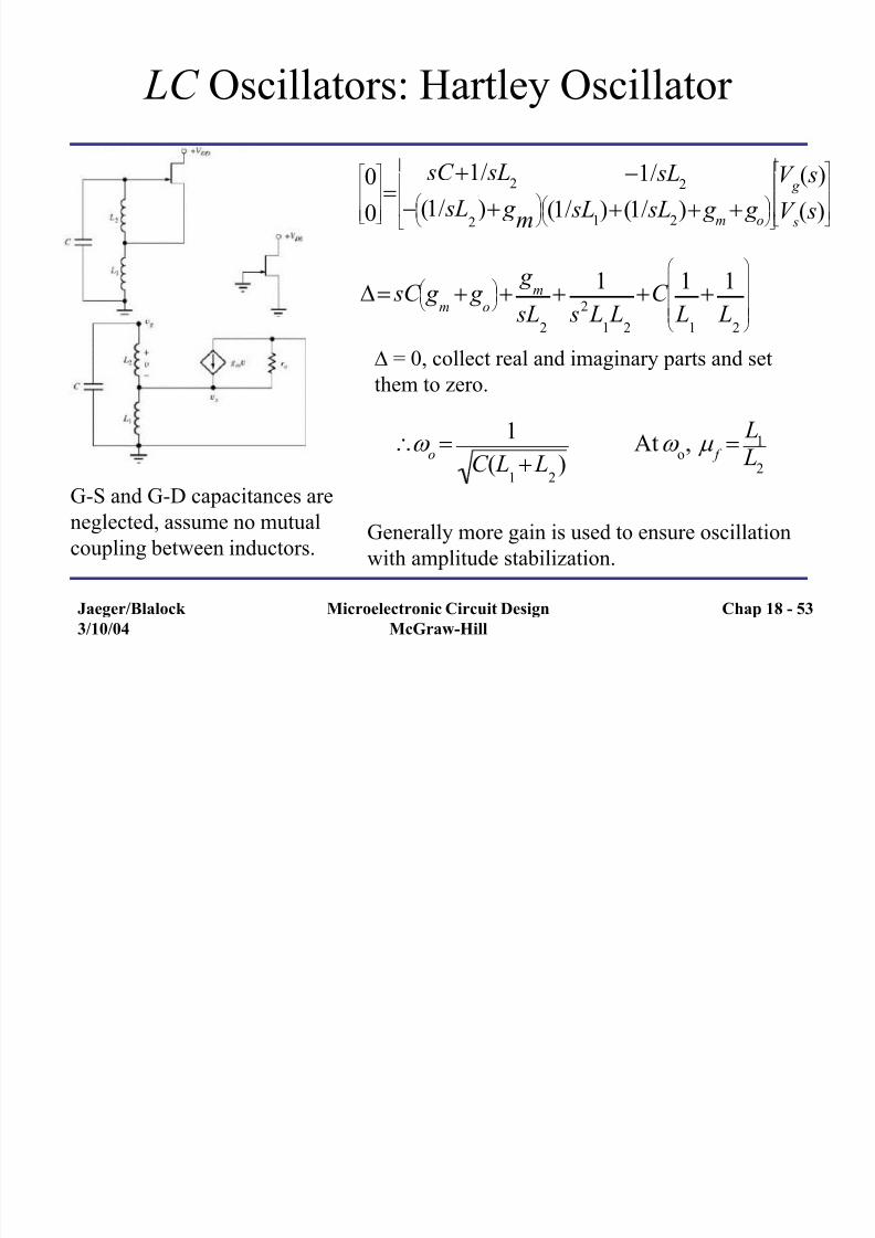
7/27/2019 Chap18-Feedback, Stability and Oscillators
http://slidepdf.com/reader/full/chap18-feedback-stability-and-oscillators 53/58
7/27/2019 Chap18-Feedback, Stability and Oscillators
http://slidepdf.com/reader/full/chap18-feedback-stability-and-oscillators 54/58
Jaeger/Blalock
3/10/04
Microelectronic Circuit Design
McGraw-Hill
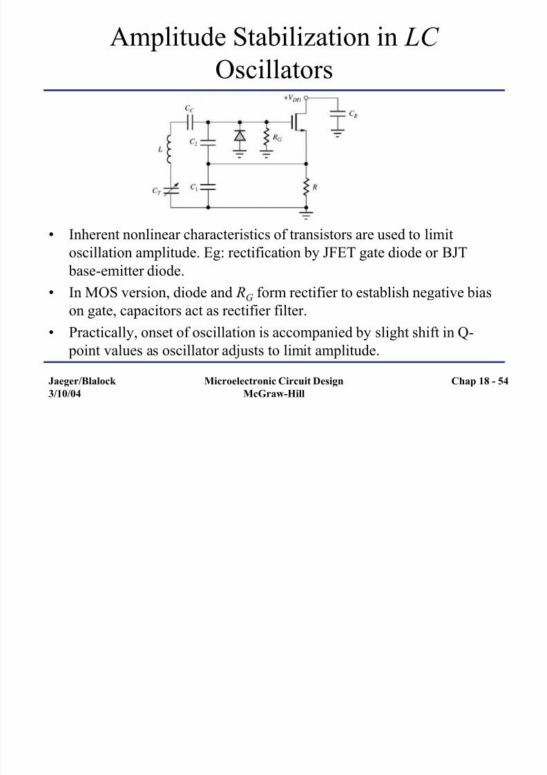
Amplitude Stabilization in LC
Oscillators
• Inherent nonlinear characteristics of transistors are used to limit
oscillation amplitude. Eg: rectification by JFET gate diode or BJT
base-emitter diode.
• In MOS version, diode and RG form rectifier to establish negative biason gate, capacitors act as rectifier filter.
• Practically, onset of oscillation is accompanied by slight shift in Q-
point values as oscillator adjusts to limit amplitude.
Chap 18 - 54
7/27/2019 Chap18-Feedback, Stability and Oscillators
http://slidepdf.com/reader/full/chap18-feedback-stability-and-oscillators 55/58
Jaeger/Blalock
3/10/04
Microelectronic Circuit Design
McGraw-Hill
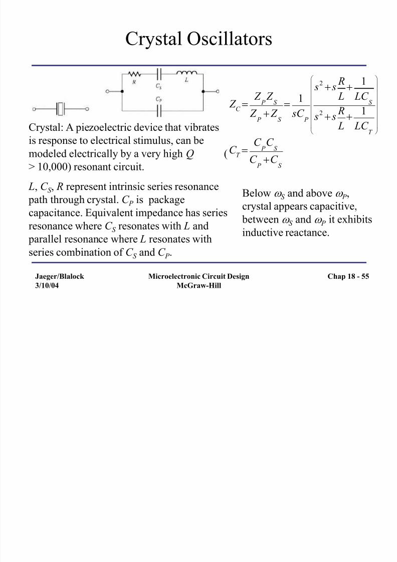
Crystal Oscillators
Crystal: A piezoelectric device that vibrates
is response to electrical stimulus, can bemodeled electrically by a very high Q (
> 10,000) resonant circuit.
L, C S , R represent intrinsic series resonance
path through crystal. C P is package
capacitance. Equivalent impedance has seriesresonance where C S resonates with L and
parallel resonance where L resonates with
series combination of C S and C P .
Z C
Z
P Z
S
Z P
Z S
1
sC P
s2 s R
L 1
LC S
s2 s R
L 1
LC T
C T
C P C S
C P
C S
Below S and above P ,
crystal appears capacitive,
between S and P it exhibits
inductive reactance.
Chap 18 - 55
7/27/2019 Chap18-Feedback, Stability and Oscillators
http://slidepdf.com/reader/full/chap18-feedback-stability-and-oscillators 56/58
Jaeger/Blalock
3/10/04
Microelectronic Circuit Design
McGraw-Hill
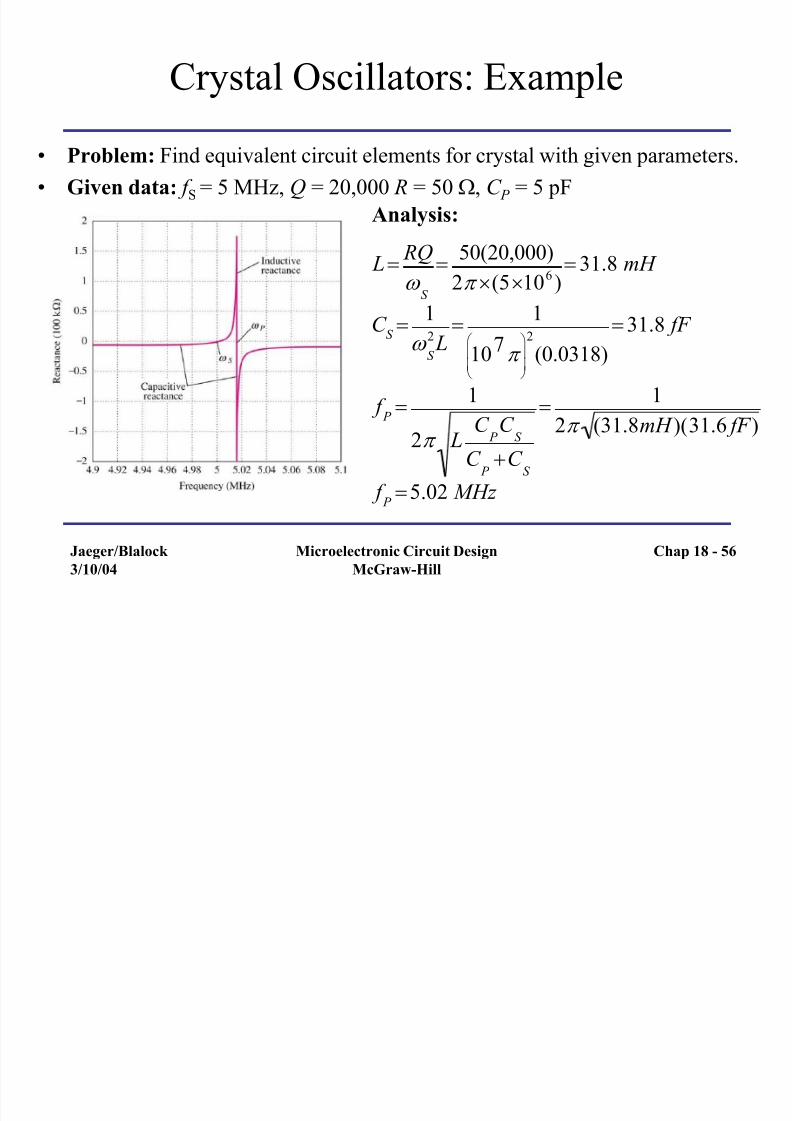
Crystal Oscillators: Example
• Problem: Find equivalent circuit elements for crystal with given parameters.
• Given data: f S = 5 MHz, Q = 20,000 R = 50 W, C P = 5 pF
Analysis:
L RQ
S
50(20,000)
2 (5106
)
31.8 mH
C S
1
S
2 L 1
107
2
(0.0318)
31.8 fF
f P
1
2 L C P C S
C P
C S
1
2 (31.8mH )(31.6 fF )
f P
5.02 MHz
Chap 18 - 56
7/27/2019 Chap18-Feedback, Stability and Oscillators
http://slidepdf.com/reader/full/chap18-feedback-stability-and-oscillators 57/58
Jaeger/Blalock
3/10/04
Microelectronic Circuit Design
McGraw-Hill
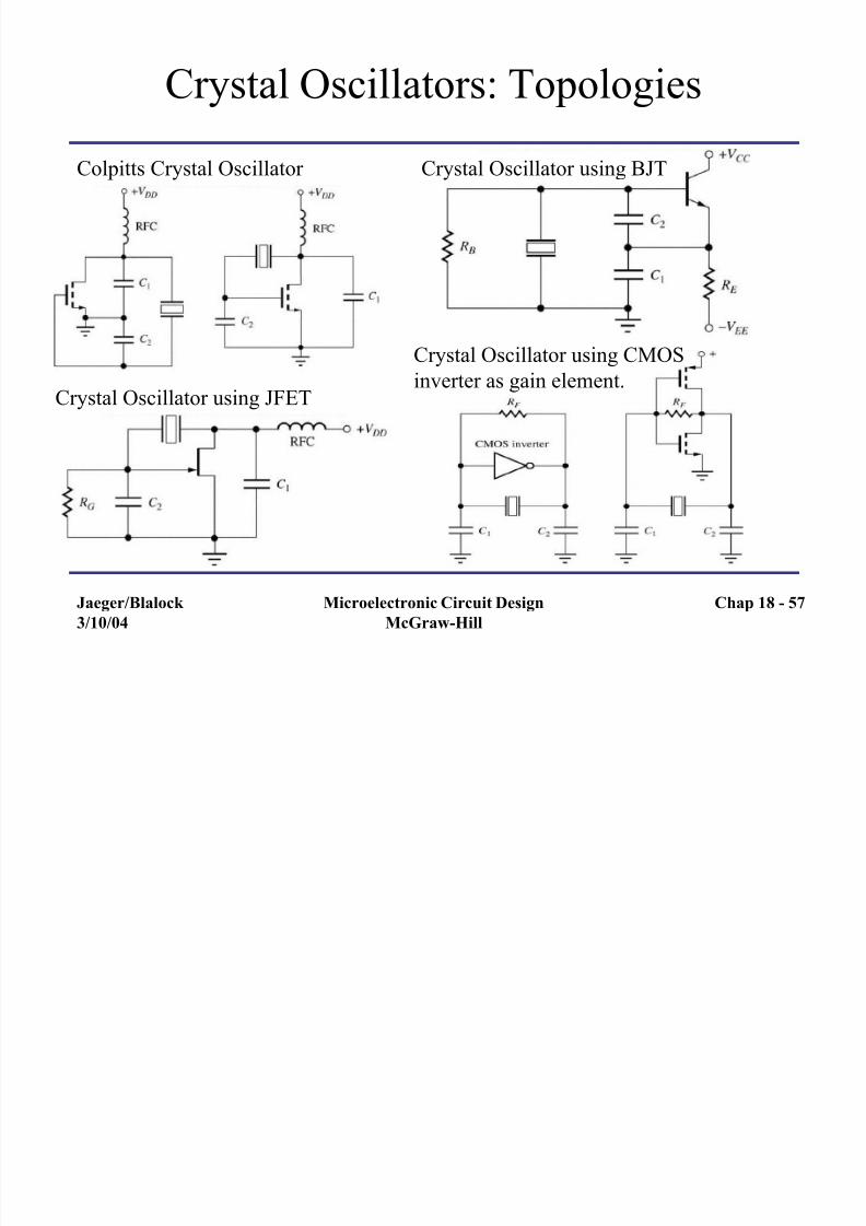
Crystal Oscillators: Topologies
Colpitts Crystal Oscillator Crystal Oscillator using BJT
Crystal Oscillator using JFET
Crystal Oscillator using CMOS
inverter as gain element.
Chap 18 - 57
7/27/2019 Chap18-Feedback, Stability and Oscillators
http://slidepdf.com/reader/full/chap18-feedback-stability-and-oscillators 58/58
J /Bl l k Mi l t i Ci it D i
End of Chpater 18


![Chap18[1] the Statement of Cashflows](https://static.fdocuments.net/doc/165x107/55cf9942550346d0339c7445/chap181-the-statement-of-cashflows.jpg)