Chap. 7 Counters and Registers
24
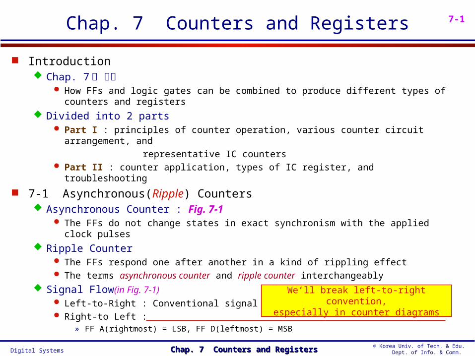
Digital Systems © Korea Univ. of Tech. & Edu. Dept. of Info. & Comm. Chap. 7 Counters and Registers Chap. 7 Counters and Registers 7-1 Chap. 7 Counters and Registers Introduction Chap. 7 의 의의 How FFs and logic gates can be combined to produce different types of counters and registers Divided into 2 parts Part I : principles of counter operation, various counter circuit arrangement, and representative IC counters Part II : counter application, types of IC register, and troubleshooting 7-1 Asynchronous(Ripple) Counters Asynchronous Counter : Fig. 7-1 The FFs do not change states in exact synchronism with the applied clock pulses Ripple Counter The FFs respond one after another in a kind of rippling effect The terms asynchronous counter and ripple counter interchangeably Signal Flow(in Fig. 7-1) Left-to-Right : Conventional signal flow Right-to Left : » FF A(rightmost) = LSB, FF D(leftmost) = MSB We’ll break left-to-right convention, especially in counter diagrams
-
Upload
jerry-nunez -
Category
Documents
-
view
87 -
download
1
description
Chap. 7 Counters and Registers. Introduction Chap. 7 의 내용 How FFs and logic gates can be combined to produce different types of counters and registers Divided into 2 parts Part I : principles of counter operation, various counter circuit arrangement, and - PowerPoint PPT Presentation
Transcript of Chap. 7 Counters and Registers
Digital Systems© Korea Univ. of Tech. & Edu. Dept. of Info. & Comm.Chap. 7 Counters and RegistersChap. 7 Counters and Registers
7-1Chap. 7 Counters and Registers
Introduction Chap. 7 의 내용
How FFs and logic gates can be combined to produce different types of counters and registers
Divided into 2 parts Part I : principles of counter operation, various counter circuit arrangement, and
representative IC counters Part II : counter application, types of IC register, and troubleshooting
7-1 Asynchronous(Ripple) Counters Asynchronous Counter : Fig. 7-1
The FFs do not change states in exact synchronism with the applied clock pulses
Ripple Counter The FFs respond one after another in a kind of rippling effect The terms asynchronous counter and ripple counter interchangeably
Signal Flow(in Fig. 7-1) Left-to-Right : Conventional signal flow Right-to Left :
» FF A(rightmost) = LSB, FF D(leftmost) = MSB
We’ll break left-to-right convention, especially in counter diagrams
Digital Systems© Korea Univ. of Tech. & Edu. Dept. of Info. & Comm.Chap. 7 Counters and RegistersChap. 7 Counters and Registers
7-2
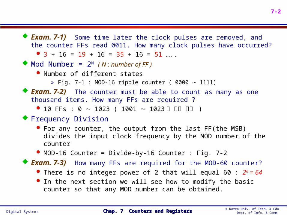
Exam. 7-1) Some time later the clock pulses are removed, and the counter FFs read 0011. How many clock pulses have occurred?
3 + 16 = 19 + 16 = 35 + 16 = 51 ….. Mod Number = 2N ( N : number of FF )
Number of different states» Fig. 7-1 : MOD-16 ripple counter ( 0000 1111)
Exam. 7-2) The counter must be able to count as many as one thousand items. How many FFs are required ?
10 FFs : 0 1023 ( 1001 1023 은 필요 없음 )
Frequency Division For any counter, the output from the last FF(the MSB) divides the input clock
frequency by the MOD number of the counter MOD-16 Counter = Divide-by-16 Counter : Fig. 7-2
Exam. 7-3) How many FFs are required for the MOD-60 counter? There is no integer power of 2 that will equal 60 : 26 = 64 In the next section we will see how to modify the basic counter so that any MOD
number can be obtained.
Digital Systems© Korea Univ. of Tech. & Edu. Dept. of Info. & Comm.Chap. 7 Counters and RegistersChap. 7 Counters and Registers
7-3
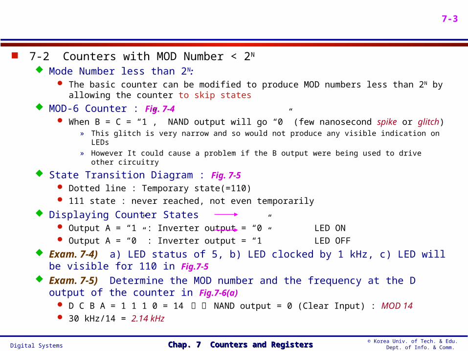
7-2 Counters with MOD Number < 2N
Mode Number less than 2N: The basic counter can be modified to produce MOD numbers less than 2N by allowing the
counter to skip states MOD-6 Counter : Fig. 7-4
When B = C = “1”, NAND output will go “0” (few nanosecond spike or glitch)» This glitch is very narrow and so would not produce any visible indication on LEDs» However It could cause a problem if the B output were being used to drive other circuitry
State Transition Diagram : Fig. 7-5 Dotted line : Temporary state(=110) 111 state : never reached, not even temporarily
Displaying Counter States Output A = “1” : Inverter output = “0” LED ON Output A = “0” : Inverter output = “1” LED OFF
Exam. 7-4) a) LED status of 5, b) LED clocked by 1 kHz, c) LED will be visible for 110 in Fig.7-5
Exam. 7-5) Determine the MOD number and the frequency at the D output of the counter in Fig.7-6(a)
D C B A = 1 1 1 0 = 14 일 때 NAND output = 0 (Clear Input) : MOD 14 30 kHz/14 = 2.14 kHz
Digital Systems© Korea Univ. of Tech. & Edu. Dept. of Info. & Comm.Chap. 7 Counters and RegistersChap. 7 Counters and Registers
7-4
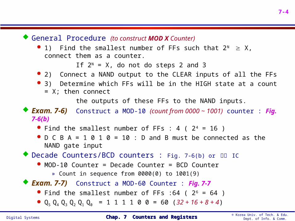
General Procedure (to construct MOD X Counter) 1) Find the smallest number of FFs such that 2N X, connect them as a counter.
If 2N = X, do not do steps 2 and 3 2) Connect a NAND output to the CLEAR inputs of all the FFs 3) Determine which FFs will be in the HIGH state at a count = X; then connect
the outputs of these FFs to the NAND inputs. Exam. 7-6) Construct a MOD-10 (count from 0000 ~ 1001) counter : Fig. 7-6(b)
Find the smallest number of FFs : 4 ( 24 = 16 ) D C B A = 1 0 1 0 = 10 : D and B must be connected as the NAND gate input
Decade Counters/BCD counters : Fig. 7-6(b) or 별도 IC
MOD-10 Counter = Decade Counter = BCD Counter » Count in sequence from 0000(0) to 1001(9)
Exam. 7-7) Construct a MOD-60 Counter : Fig. 7-7 Find the smallest number of FFs :64 ( 26 = 64 ) Q5 Q4 Q3 Q2 Q1 Q0 = 1 1 1 1 0 0 = 60 (32 + 16 + 8 + 4)
Digital Systems© Korea Univ. of Tech. & Edu. Dept. of Info. & Comm.Chap. 7 Counters and RegistersChap. 7 Counters and Registers
7-5
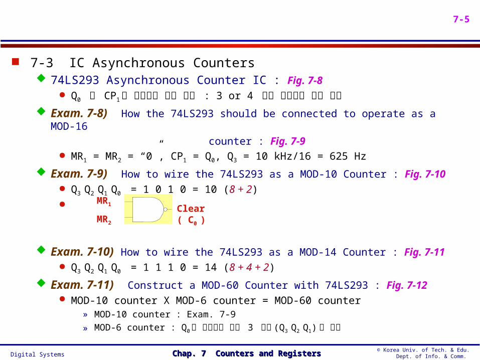
7-3 IC Asynchronous Counters 74LS293 Asynchronous Counter IC : Fig. 7-8
Q0 와 CP1 이 연결되지 않은 이유 : 3 or 4 비트 카운터로 사용 가능 Exam. 7-8) How the 74LS293 should be connected to operate as a MOD-16
counter : Fig. 7-9 MR1 = MR2 = “0”, CP1 = Q0, Q3 = 10 kHz/16 = 625 Hz
Exam. 7-9) How to wire the 74LS293 as a MOD-10 Counter : Fig. 7-10 Q3 Q2 Q1 Q0 = 1 0 1 0 = 10 (8 + 2)
Exam. 7-10) How to wire the 74LS293 as a MOD-14 Counter : Fig. 7-11 Q3 Q2 Q1 Q0 = 1 1 1 0 = 14 (8 + 4 + 2)
Exam. 7-11) Construct a MOD-60 Counter with 74LS293 : Fig. 7-12 MOD-10 counter X MOD-6 counter = MOD-60 counter
» MOD-10 counter : Exam. 7-9
» MOD-6 counter : Q0 는 사용하지 않고 3 비트 (Q3 Q2 Q1) 만 사용
MR1
MR2
Clear ( C0 )
Digital Systems© Korea Univ. of Tech. & Edu. Dept. of Info. & Comm.Chap. 7 Counters and RegistersChap. 7 Counters and Registers
7-6
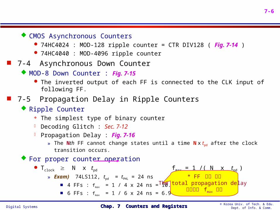
CMOS Asynchronous Counters 74HC4024 : MOD-128 ripple counter = CTR DIV128 ( Fig. 7-14 ) 74HC4040 : MOD-4096 ripple counter
7-4 Asynchronous Down Counter MOD-8 Down Counter : Fig. 7-15
The inverted output of each FF is connected to the CLK input of following FF.
7-5 Propagation Delay in Ripple Counters Ripple Counter
The simplest type of binary counter Decoding Glitch : Sec. 7-12 Propagation Delay : Fig. 7-16
» The Nth FF cannot change states until a time N x tpd after the clock transition occurs.
For proper counter operation Tclock N x tpd fmax = 1 /( N x tpd )
» Exam) 74LS112, tpd = tPHL = 24 ns
4 FFs : fmax = 1 / 4 x 24 ns = 10.4 MHz 6 FFs : fmax = 1 / 6 x 24 ns = 6.9 MHz
* FF 개수 증가The total propagation delay
증가하고 fmax 감소
Digital Systems© Korea Univ. of Tech. & Edu. Dept. of Info. & Comm.Chap. 7 Counters and RegistersChap. 7 Counters and Registers
7-7
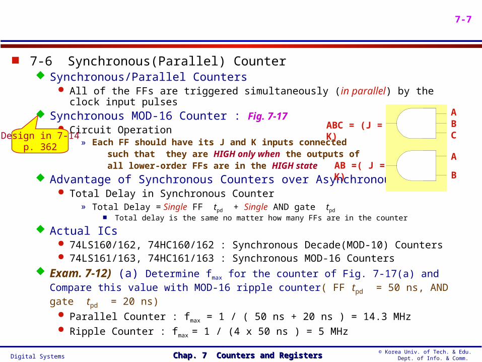
7-6 Synchronous(Parallel) Counter Synchronous/Parallel Counters
All of the FFs are triggered simultaneously (in parallel) by the clock input pulses Synchronous MOD-16 Counter : Fig. 7-17
Circuit Operation» Each FF should have its J and K inputs connected such that they are HIGH only when the outputs of all lower-order FFs are in the HIGH state
Advantage of Synchronous Counters over Asynchronous Total Delay in Synchronous Counter
» Total Delay = Single FF tpd + Single AND gate tpd Total delay is the same no matter how many FFs are in the counter
Actual ICs 74LS160/162, 74HC160/162 : Synchronous Decade(MOD-10) Counters 74LS161/163, 74HC161/163 : Synchronous MOD-16 Counters
Exam. 7-12) (a) Determine fmax for the counter of Fig. 7-17(a) and Compare this value with MOD-16 ripple counter( FF tpd = 50 ns, AND gate tpd = 20 ns)
Parallel Counter : fmax = 1 / ( 50 ns + 20 ns ) = 14.3 MHz Ripple Counter : fmax = 1 / (4 x 50 ns ) = 5 MHz
ABC
A
B
ABC = (J = K)
AB =( J = K)
Design in 7-14p. 362
Digital Systems© Korea Univ. of Tech. & Edu. Dept. of Info. & Comm.Chap. 7 Counters and RegistersChap. 7 Counters and Registers
7-8
(b) What must be done to convert this counter to MOD-32 5 개째 FF(25 = 32) 이 추가되며 , J and K input are fed by the output of
a four input AND gate whose inputs are A, B, C, and D
(c) Determine fmax for the MOD-32 parallel counter FF 개수에 관계없이 14.3 MHz
7-7 Synchronous Down and Up/Down Counters MOD-8 Parallel Up/Down Counter : Fig. 7-18
Up Count : Up/Down = 1, AND gates 1/2 = Enabled, AND gates 3/4 = Disabled Down Count : Up/Down = 0, AND gates 1/2 = Disabled, AND gates 3/4 = Enabled
Exam. 7-13) What problems might be caused if the Up/Down signal changes levels on the NGT of the clock ?
Possible Problems : Unpredictable results of FF» the J and K inputs change at about the same time that a NGT occurs at their CLK input
. Effects : Predictable results of FF(No problems)
» the effects of the change in the control signal must propagate through two gates before reaching the J, K inputs( 결국 다음 Clock 에서 Up/Down 동작이 가능함 )
Digital Systems© Korea Univ. of Tech. & Edu. Dept. of Info. & Comm.Chap. 7 Counters and RegistersChap. 7 Counters and Registers
7-9
7-8 Presettable Counters Presettable Counter/Parallel Loading Counter
Preset to any desired starting count either asynchronously or synchronously Presettable Parallel Counter with Asynchronous Preset : Fig. 7-19
The counter is loaded with any desired count at any time» 1) Apply the desired count to the parallel data inputs, P2, P1, and P0
» 2) Apply a Low pulse to the PARALLEL LOAD input(PL) PL 은 Active Low 이고 , 이 때 2 개 NAND Gate 의 한 개 입력은 항상 1,
따라서 P 에 의해 P = 1 이면 PRESET, 그리고 P = 0 이면 CLR Asynchronous Presetting IC Counters
» TTL : 74LS190, 191, 192, 193
» CMOS : 74HC190, 191, 192, 193
Synchronous Presetting The counter is preset on the active transition of the same clock signal Synchronous Presetting IC Counters
» TTL : 74LS160, 161, 162, 163
» CMOS : 74HC160, 161, 162, 163
Async presetting 에서는 PRE/CLR 에 의해
Digital Systems© Korea Univ. of Tech. & Edu. Dept. of Info. & Comm.Chap. 7 Counters and RegistersChap. 7 Counters and Registers
7-10
7-9 The 74LS193/HC193 Presettable Up/Down Counter(74LS193) : Fig. 7-20
Synchronous Counter, Asynchronous Preset, and Asynchronous Master Reset Terminal Count : Fig. 7-21
» TCU : 1111 0000 ( Fig. 7-22 에서 t6, t7 참고 )
» TCD : 0000 1111 ( Fig. 7-23 에서 t9, t10 참고 )
Exam. 7-14) Determine the counter output waveforms in Fig. 7-22(a) Up Counter : Fig. 7-22(b)
Exam. 7-15) Determine the counter output waveforms in Fig. 7-23(a) Down Counter : Fig. 7-23(b)
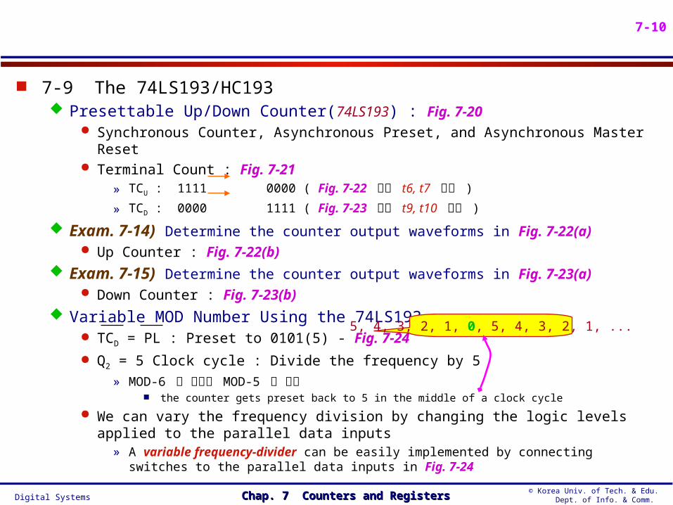
Variable MOD Number Using the 74LS193 TCD = PL : Preset to 0101(5) - Fig. 7-24
Q2 = 5 Clock cycle : Divide the frequency by 5
» MOD-6 가 아니고 MOD-5 인 이유 the counter gets preset back to 5 in the middle of a clock cycle
We can vary the frequency division by changing the logic levels applied to the parallel data inputs
» A variable frequency-divider can be easily implemented by connecting switches to the parallel data inputs in Fig. 7-24
5, 4, 3, 2, 1, 0, 5, 4, 3, 2, 1, ...
Digital Systems© Korea Univ. of Tech. & Edu. Dept. of Info. & Comm.Chap. 7 Counters and RegistersChap. 7 Counters and Registers
7-11
Multistage Arrangement : Fig. 7-25 8 bits Up/Down Counter using two 74LS193s
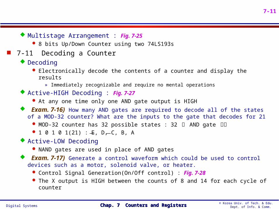
7-11 Decoding a Counter Decoding
Electronically decode the contents of a counter and display the results» Immediately recognizable and require no mental operations
Active-HIGH Decoding : Fig. 7-27 At any one time only one AND gate output is HIGH
Exam. 7-16) How many AND gates are required to decode all of the states of a MOD-32 counter? What are the inputs to the gate that decodes for 21
MOD-32 counter has 32 possible states : 32 개 AND gate 필요 1 0 1 0 1(21) : E, D, C, B, A
Active-LOW Decoding NAND gates are used in place of AND gates
Exam. 7-17) Generate a control waveform which could be used to control devices such as a motor, solenoid valve, or heater.
Control Signal Generation(On/Off control) : Fig. 7-28 The X output is HIGH between the counts of 8 and 14 for each cycle of counter
Digital Systems© Korea Univ. of Tech. & Edu. Dept. of Info. & Comm.Chap. 7 Counters and RegistersChap. 7 Counters and Registers
7-12
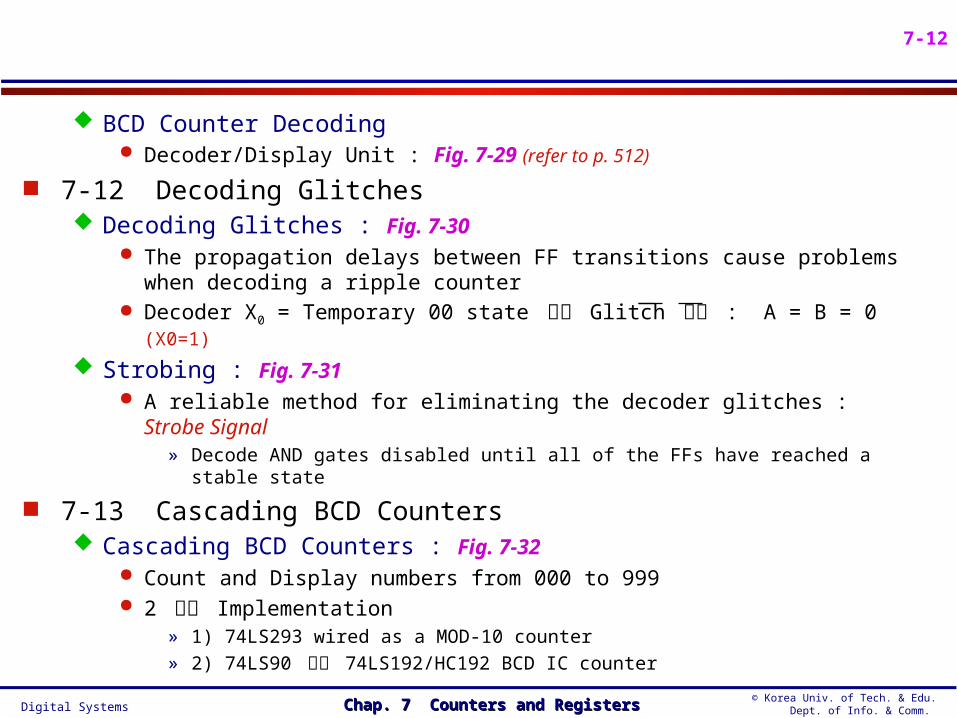
BCD Counter Decoding Decoder/Display Unit : Fig. 7-29 (refer to p. 512)
7-12 Decoding Glitches Decoding Glitches : Fig. 7-30
The propagation delays between FF transitions cause problems when decoding a ripple counter
Decoder X0 = Temporary 00 state 에서 Glitch 발생 : A = B = 0 (X0=1)
Strobing : Fig. 7-31 A reliable method for eliminating the decoder glitches : Strobe Signal
» Decode AND gates disabled until all of the FFs have reached a stable state
7-13 Cascading BCD Counters Cascading BCD Counters : Fig. 7-32
Count and Display numbers from 000 to 999 2 가지 Implementation
» 1) 74LS293 wired as a MOD-10 counter
» 2) 74LS90 또는 74LS192/HC192 BCD IC counter
Digital Systems© Korea Univ. of Tech. & Edu. Dept. of Info. & Comm.Chap. 7 Counters and RegistersChap. 7 Counters and Registers
7-13
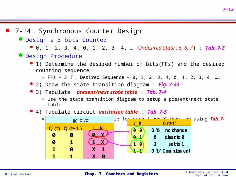
7-14 Synchronous Counter Design Design a 3 bits Counter
0, 1, 2, 3, 4, 0, 1, 2, 3, 4, … (Undesired State : 5, 6, 7) : Tab. 7-3
Design Procedure 1) Determine the desired number of bits(FFs) and the desired counting sequence
» FFs = 3 개 , Desired Sequence = 0, 1, 2, 3, 4, 0, 1, 2, 3, 4, …. 2) Draw the state transition diagram : Fig. 7-33 3) Tabulate present/next state table : Tab. 7-4
» Use the state transition diagram to setup a present/next state table 4) Tabulate circuit excitation table : Tab. 7-5
» Add a column to this table for each J and K input by using Tab. 7-2
Q(t) Q(t+1) J K 0 0 0 X 0 1 1 X 1 0 X 1 1 1 X 0
J K F/F J K0 00 11 01 1 Q(t)' Complement
Q(t+1) Q(t) no change 0 clear to 0 1 set to 1
Digital Systems© Korea Univ. of Tech. & Edu. Dept. of Info. & Comm.Chap. 7 Counters and RegistersChap. 7 Counters and Registers
7-14
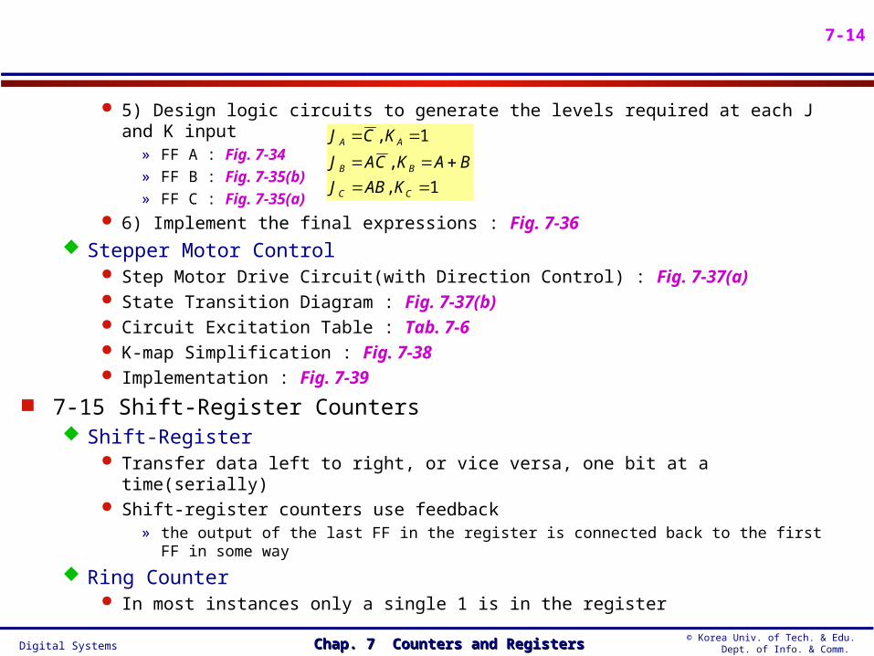
5) Design logic circuits to generate the levels required at each J and K input» FF A : Fig. 7-34
» FF B : Fig. 7-35(b)
» FF C : Fig. 7-35(a) 6) Implement the final expressions : Fig. 7-36
Stepper Motor Control Step Motor Drive Circuit(with Direction Control) : Fig. 7-37(a) State Transition Diagram : Fig. 7-37(b) Circuit Excitation Table : Tab. 7-6 K-map Simplification : Fig. 7-38 Implementation : Fig. 7-39
7-15 Shift-Register Counters Shift-Register
Transfer data left to right, or vice versa, one bit at a time(serially) Shift-register counters use feedback
» the output of the last FF in the register is connected back to the first FF in some way
Ring Counter In most instances only a single 1 is in the register
1,
,
1,
CC
BB
AA
KABJ
BAKCAJ
KCJ
Digital Systems© Korea Univ. of Tech. & Edu. Dept. of Info. & Comm.Chap. 7 Counters and RegistersChap. 7 Counters and Registers
7-15
MOD-4 Ring Counter : Fig. 7-40» Ring counters can be constructed for any desired MOD number
A MOD-N ring counter used N flip-flops
Starting a Ring Counter A ring counter must start off with only one FF in the 1 state and all the others in
the 0 state Ring Counter Starter : Fig. 7-41
» 1) On power-up, the capacitor will charge up relatively slowly toward Vcc, 따라서 Inverter 1 input = 0
» 2) Inverter 1 output = 1, 따라서 Inverter 2 output = 0 until Inverter 1 input = 1 이때 Q3 = PRE, Q2 = Q1 = Q0 = CLR 임으로 1 0 0 0 으로 Preset 됨
Johnson Counter/Twisted Ring Counter The inverted output of the last FF is connected to the input of the first FF 3 bits Johnson counter : Fig. 7-42
» MOD-6(six distinct states) : 000, 100, 110, 111, 011, and 001
» 50 percent duty cycle square wave at one-sixth the frequency of the clock
» MOD-N counter(N= even number) by connecting N/2 FFs MOD-10 Johnson Counter : 5 FF 필요
4 distinct states
Digital Systems© Korea Univ. of Tech. & Edu. Dept. of Info. & Comm.Chap. 7 Counters and RegistersChap. 7 Counters and Registers
7-16
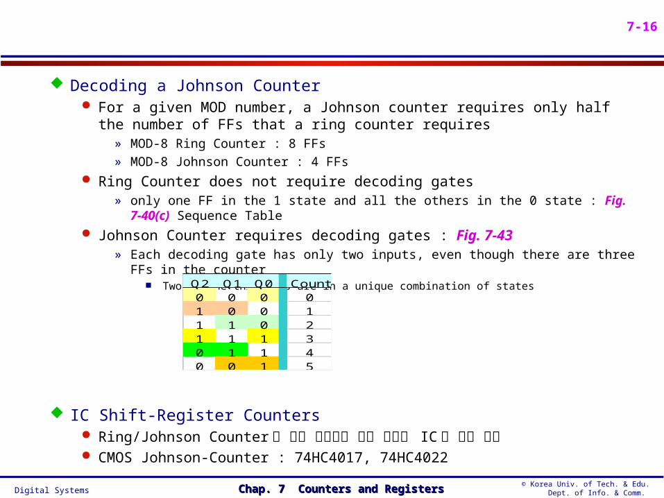
Decoding a Johnson Counter For a given MOD number, a Johnson counter requires only half the number of
FFs that a ring counter requires» MOD-8 Ring Counter : 8 FFs
» MOD-8 Johnson Counter : 4 FFs Ring Counter does not require decoding gates
» only one FF in the 1 state and all the others in the 0 state : Fig. 7-40(c) Sequence Table
Johnson Counter requires decoding gates : Fig. 7-43» Each decoding gate has only two inputs, even though there are three FFs in the
counter Two of the three FFs are in a unique combination of states
IC Shift-Register Counters Ring/Johnson Counter 는 너무 간단하게 구현 됨으로 IC 가 별로 없다 CMOS Johnson-Counter : 74HC4017, 74HC4022
Q2 Q1 Q0 Count0 0 0 01 0 0 11 1 0 21 1 1 30 1 1 40 0 1 5
Digital Systems© Korea Univ. of Tech. & Edu. Dept. of Info. & Comm.Chap. 7 Counters and RegistersChap. 7 Counters and Registers
7-17
7-16 Counter Applications : Frequency Counter Frequency Counter : Fig. 7-44
Counter + Decoder/Display + AND gate Sampling Interval : SAMPLE pulse goes HIGH from t1 to t2
» During this sampling interval the unknown frequency pulses(fx) will pass through the AND gate and will be counted by the counter
» The accuracy of this method depends almost entirely on the duration of the sampling interval
The sampling Interval must be very accurately controlled
Exam. 7-18) The unknown frequency is 3792 pulses per second(pps). Determine the counter reading after a sampling interval of (a) 1 s, (b) 0.1 s, and (c)10ms
(a) 1 s : 3792 (b) 0.1 s : 379.2, 379 or 380 (c) 0.01 s : 37.92, 37 or 38 A method for obtaining accurate sampling interval : Fig. 7-45
Crystal Oscillator : generate a very accurate 100-kHz waveform Decade Counter : divide 100-kHz frequency by 10 Rotary Switch : select one of the decade-counter output Flip-Flop : 2 분주
» In position 1 : 1 Hz / 2 = 0.5 Hz Q = 0.5 Hz = 1 / 0.5 Hz = 2 T, 따라서 HIGH 상태의 반주기는 T (Sampling Interval)
Digital Systems© Korea Univ. of Tech. & Edu. Dept. of Info. & Comm.Chap. 7 Counters and RegistersChap. 7 Counters and Registers
7-18
Exam. 7-19) The unknown input frequency is between 1, 000 pps and 9,990 pps, what is the best setting for the switch position in Fig. 7-45 with 3 BCD counter and display.
With three BCD counter : total capacity = 000 - 999» 0.1 s sampling interval : 100 - 999
Complete Frequency Counter : Fig. 7-46 X : FF 의 출력 (= One-shot 의 Clock input)
» SAMPLE pulse 의 2 분주이고 100ns One-shot pulse 를 Trigger 시켜 Counter 를 Clear 함 .
» AND gate 에 의해 SAMPLE pulse 와 X 가 모두 HIGH 일 때만 Counter 동작 예제 ) Sampling Interval = 1 s, 그리고 unknown frequency = 237 pps 인 경우
» t1 - t2 : X = 0 으로 동작하지 않음» t2 - t3 : Counter is cleared to 0 and display 0 for 1 s ( = sample interval = 1 s )
» t3 - t4 : Counter 는 1 s 동안 0 - 237 까지 Count
» t4 - t6 : 2 s 동안 237 Display
7-17 Counter Application : Digital Clock Digital Clock operating from 60 Hz : Fig. 7-47
Schmitt-trigger circuit : produce square pulses at the rate of 60 pps MOD-60 Counter : divide the 60 pps down to 1 pps
Digital Systems© Korea Univ. of Tech. & Edu. Dept. of Info. & Comm.Chap. 7 Counters and RegistersChap. 7 Counters and Registers
7-19
Detailed Hour Section : Fig. 7-48 MOD-2 ( 0 -1 ) + MOD-10 ( 0 - 9 ) Counter
» MOD-10 Counter : 74LS192(Presettable BCD Counter)
» MOD-2 Counter : JK Flip-Flop
» 12 에서 13 이 될 때 74LS192 의 PL 에 의해 상위 시간 = 0 (74LS112 는 Clear), 그리고 하위 시간 = 1( P3 P2 P1 P0 = 0 0 0 1) 이 된다 .
3 Input NAND gate 에서 상위 시간 X = 1, 그리고 하위 시간 Q1 Q0 = 11(3) 일 때 PL Enabled
» Q3 = 1, 즉 하위 시간 = 9 일 때 상위 시간 = 1 이 된다 ( 09 10).
7-18 IC Registers 1) Parallel in/Parallel out : 74174, 74178 2) Serial in/Serial out : 4731B 3) Parallel in/Serial out : 74165 4) Serial in/Parallel out : 74164
7-19 Parallel in/Parallel out : 74174 and 74178 74174 and 74HC174( 6 bit register ) : Fig. 7-49
Digital Systems© Korea Univ. of Tech. & Edu. Dept. of Info. & Comm.Chap. 7 Counters and RegistersChap. 7 Counters and Registers
7-20
Exam. 7-20A) How to connect 74ALS174 so that D5 D4 D3 D2 D1 D0 ( = data input at D5 and data output at Q0 ).
Fig. 7-50 Exam. 7-20B) How to connect two 74ALS174 to operate as a 12 bit shift register.
Connect the Q0 of the first IC to the D5 of the second IC.
7-20 Serial in/Serial out : 4731B 4731B(CMOS Quad 64-bit) : Fig. 7-51
64 개 D-type Flip-Flop : 4 개가 one chip 이므로 총 256 개 FF Buffer circuit : Q63 (triangle symbol with no inversion bubble)
» A buffer does not change the signal’s logic level
» It is used to provide a greater output-current capability than normal
Digital Systems© Korea Univ. of Tech. & Edu. Dept. of Info. & Comm.Chap. 7 Counters and RegistersChap. 7 Counters and Registers
7-21
Exam. 7-21) Delay circuit using 4731B chip : Fig. 7-52 Q63 goes HIGH approximately 64 clock cycles after Ds input
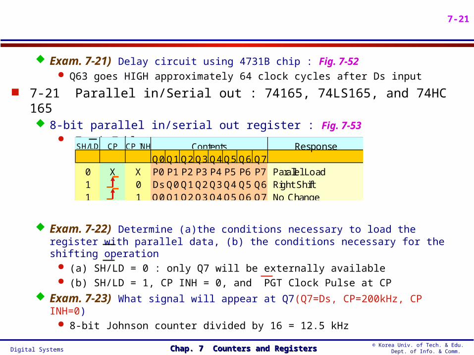
7-21 Parallel in/Serial out : 74165, 74LS165, and 74HC165 8-bit parallel in/serial out register : Fig. 7-53
Truth Table
Exam. 7-22) Determine (a)the conditions necessary to load the register with parallel data, (b) the conditions necessary for the shifting operation
(a) SH/LD = 0 : only Q7 will be externally available (b) SH/LD = 1, CP INH = 0, and PGT Clock Pulse at CP
Exam. 7-23) What signal will appear at Q7(Q7=Ds, CP=200kHz, CP INH=0) 8-bit Johnson counter divided by 16 = 12.5 kHz
SH/LD CP CP INH ResponseQ0Q1Q2Q3Q4Q5 Q6 Q7
0 X X P0 P1 P2 P3 P4 P5 P6 P7 Parallel Load1 0 Ds Q0Q1Q2Q3Q4 Q5 Q6 Right Shift1 1 Q0Q1Q2Q3Q4Q5 Q6 Q7 No Change
Contents
Digital Systems© Korea Univ. of Tech. & Edu. Dept. of Info. & Comm.Chap. 7 Counters and RegistersChap. 7 Counters and Registers
7-22
7-22 Serial in/Parallel out : 74164, 74LS164, and 74HC164 8-bit serial in/parallel out shift register : Fig. 7-54
Each FF output externally accessible : Q0, Q1, …, Q7 2 input AND gate : one input can be used for control
Exam. 7-24) Determine the sequence of states in Fig. 7-55(a) (Initial Content of the 74ALS164 = 00000000)
The correct sequence : Fig. 7-57(b)» Q7 =1 : Temporary state
LOW at MR ( inverted Q7 ) resets the register back to 00000000
Other Register ICs 74194/LS194/HC194 : 4 bit bi-directional universal shift register
4 mode : shift left, shift right, parallel in, parallel out ( selected by 2 bit mode select code as inputs )
74373/LS373/HC373 : 8 bit parallel in/parallel out register 8 D latch with tri-state outputs : Data or Address bus buffer 로 주로 사용됨
» Pin 11 : Latch Enable(LE) 로 Level trigger = 1 일 때 8 개 입력 D0 - D7 이 8 개 출력 Q0 - Q7 으로 출력됨 ( 따라서 Transparent Latch 라고도 함 )
74374/LS374/HC374 : 8 bit parallel in/parallel out register 8 edge-triggered D Flip-Flops with tri-state outputs
» Pin 11 : Clock Pulse(CP) 로 Edge trigger(PGT) 일 때 373 과 마찬가지로 출력됨
Digital Systems© Korea Univ. of Tech. & Edu. Dept. of Info. & Comm.Chap. 7 Counters and RegistersChap. 7 Counters and Registers
7-23
7-24 Trouble Shooting Exam. 7-25) Determine the possible faults of MOD-10 counter in Fig. 7-57(a) ( The
displayed waveforms of the Q output with an oscilloscope are shown in Fig. 7-57(b) ) 이상 증상 : Q1, Q2, and Q3(except Q0) are stuck in the LOW state 이상 가능성 :
» 1) Q1 : internally or externally shorted to ground» 2) MR1 : internally shorted to ground (Q1=0)» 3) Q0 와 CP1 사이의 Open : 따라서 Q1 이 Clock Input 을 받지 못함 » 4) IC 자체의 internal fault
Exam. 7-26) 위의 4 가지 이상 가능성을 조사했으나 모두 아니었으며 , Fig. 7-58 과 같이 Q1 에서 glitch 를 발견했음 . 이상 원인은 ?
MR2 의 Open : MR2 = HIGH in TTL » Q1 의 glitch 에 의해 항상 0 으로 reset 됨 , 따라서 MOD-2 카운터로 동작했음 ( 0, 1
) Exam. 7-27) The displayed frequency is exactly twice in Fig. 7-46, What is the
probable cause for the malfunction ? 3 input AND gate 의 가운데 입력이 Open 되었음 : SAMPLE pulse = HIGH:
» 따라서 t3 와 t4 동안만 sampling 되지 않고 , t2 와 t4 동안 sampling 되었음 . Exam. 7-28) The HOURS section displays in the manner shown in Tab. 7-7 . 이상
원인은 ? ( p. 382, Fig. 7-48 참고 ) 74LS192 의 Q3 이 아니고 Q2 가 74LS112 의 CLK 에 잘못 연결됨
» 따라서 9 0 일 때 X = 1 로 되야 하나 , 7 8 일 때 X = 1 로 되었음 .
p. 333, Fig. 7-12 참고
Digital Systems© Korea Univ. of Tech. & Edu. Dept. of Info. & Comm.Chap. 7 Counters and RegistersChap. 7 Counters and Registers
7-24
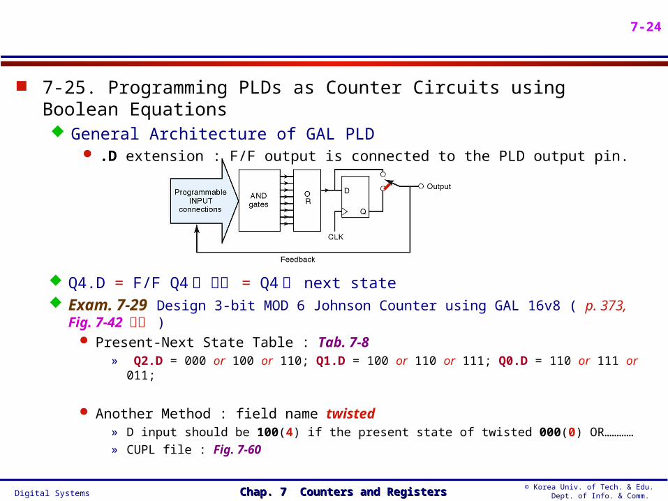
7-25. Programming PLDs as Counter Circuits using Boolean Equations General Architecture of GAL PLD
.D extension : F/F output is connected to the PLD output pin.
Q4.D = F/F Q4 의 입력 = Q4 의 next state Exam. 7-29 Design 3-bit MOD 6 Johnson Counter using GAL 16v8 ( p. 373, Fig. 7-
42 참고 ) Present-Next State Table : Tab. 7-8
» Q2.D = 000 or 100 or 110; Q1.D = 100 or 110 or 111; Q0.D = 110 or 111 or 011;
Another Method : field name twisted» D input should be 100(4) if the present state of twisted 000(0) OR…………
» CUPL file : Fig. 7-60