Challenges in Interconnection Network Design In the … · Challenges in Interconnection Network...
6
Proc. Int'[ Conf. Communications in Computing (CIC-2000) Las Vegas, Nevada, USA, 2000 June 26-29 Challenges in Interconnection Network Design In the Era of Multiprocessor and Massively Parallel Microchips Behrooz Parhami and Ding-Ming Kwai Department of Electrical and Computer Engineering University of California Santa Barbara, CA 93106-9560, USA E-mail: [email protected] Abstract Custom microchips housing many simple processors have long been used in the design ofmassively parallel computers. Commercially available SIMD!arallel systems of the late 1980s already containe tens of bit-serial processors on each chip and more recent products offer hundreds of processors per chip. Use of microchips housing multiple general-purpose processors. with large memories. has also been proposed. No matter how many processors we can put on one chip. the demandfor greater performance will sustain the need for integrating multiple chips into systems that offer even higher levels of parallelism. With tens to tens of thousands of on-cfiip processors afforded by billion-transistor chips. small-scale parallel systems built of powerful general-purpose processors. as well as multimillion-node massively parallel systems. will become not only realizable but also quite cost-effective. Our thesis is that design challenges for single-chip mUltifrocessors and massively parallel systems. as wei as their use in synthesizing even larger parallel systems. are not fundamentally different from those currently facing parallel computer designers. given that interconnects already constitute the limiting factor. Either way. we need to rely on multilevel (hierarchical or recursive) parallel architectures. The difference is in scale rather than substance. with the requisite theories and design strategies already in place. Keywords: hierarchical network, interconnect, MPP, multilevel network, parallel computer architecture, recursive network, technology scaling, wire delay. 1. Introduction Since the introduction of early MIMD-type parallel machines in the 1960s, the processing nodes in such systems have continually shrunk in size from large cabinets, to multi board assemblies, to single boards, and now to chips or small chip sets. Multiprocessor chips are already a reality, constituting a plausible way of utilizing the higher densities that are becoming available [Oluk96], [Hamm97] and chips containing many full-blown processors are eminent [ClarOO]. SIMD-type parallel processors have always enjoyed a higher integration density, given their simpler processors [parh95]. Commercial SIMD machines of the late 1980s already contained lens of bit-serial processors on each chip and more recent products offer hundreds of such processors per chip (thousands on one printed-circuit board). Therefore, it is only a matter of time before we witness many thousands of such SIMD nodes on a single microchip. Challenges in Network Design Regardless of how many processors we can put on one chip, the demand for greater performance will sustain the need for integrating multiple chips into systems with even higher levels of parallelism. In fact, it is true that the physical size of the largest supercomputer has not changed over the years, implying that with improved integration, we simply build larger systems; this is to quench the thirst for greater performance created by novel applications or larger-scale versions of existing ones. With tens to tens of thousands of processors afforded by billion-transistor chips, small- scale parallel systems utilizing powerful general- purpose processors, as well as multimillion-processor massively parallel systems, will become not only realizable but also quite cost-effective. Shrinkage in the size of processing nodes has brought about corresponding changes in the art of designing interconnection networks for parallel computers. The cabling between cabinets (once the sole interconnect medium) was augmented by backplane connectors and, later, by board-level links connecting chip-size nodes. The addition of another level, namely intrachip wires, to this hierarchy of interconnects (Fig. 1), may lead one to believe that the task of designing cost-effective high-performance interconnection networks will soon be draped with yet another layer of complexity. Will the grand scale and greater variety of interconnect types necessitate the development of completely new theories and/or design strategies? Fig. 1. Interconnect and packaging hierarchy. p. 1 of 6 CIC-2000 (Parhami & Kwai)
Transcript of Challenges in Interconnection Network Design In the … · Challenges in Interconnection Network...

Proc. Int'[ Conf. Communications in Computing (CIC-2000)Las Vegas, Nevada, USA, 2000 June 26-29
Challenges in Interconnection Network Design In the Era ofMultiprocessor and Massively Parallel Microchips
Behrooz Parhami and Ding-Ming KwaiDepartment of Electrical and Computer Engineering
University of CaliforniaSanta Barbara, CA 93106-9560, USA
E-mail: [email protected]
AbstractCustom microchips housing many simple processorshave long been used in the design ofmassively parallelcomputers. Commercially available SIMD!arallelsystems of the late 1980s already containe tens ofbit-serial processors on each chip and more recentproducts offer hundreds of processors per chip. Use ofmicrochips housing multiple general-purposeprocessors. with large memories. has also beenproposed. No matter how many processors we can puton one chip. the demandfor greater performance willsustain the need for integrating multiple chips intosystems that offer even higher levels of parallelism.With tens to tens of thousands of on-cfiip processorsafforded by billion-transistor chips. small-scale parallelsystems built of powerful general-purpose processors.as well as multimillion-node massively parallelsystems. will become not only realizable but alsoquite cost-effective. Our thesis is that designchallenges for single-chip mUltifrocessors andmassively parallel systems. as wei as their use insynthesizing even larger parallel systems. are notfundamentally different from those currently facingparallel computer designers. given that interconnectsalready constitute the limiting factor. Either way. weneed to rely on multilevel (hierarchical or recursive)parallel architectures. The difference is in scale ratherthan substance. with the requisite theories and designstrategies already in place.Keywords: hierarchical network, interconnect, MPP,multilevel network, parallel computer architecture,recursive network, technology scaling, wire delay.
1. Introduction
Since the introduction of early MIMD-type parallelmachines in the 1960s, the processing nodes in suchsystems have continually shrunk in size from largecabinets, to multi board assemblies, to single boards,and now to chips or small chip sets. Multiprocessorchips are already a reality, constituting a plausible wayof utilizing the higher densities that are becomingavailable [Oluk96], [Hamm97] and chips containingmany full-blown processors are eminent [ClarOO].
SIMD-type parallel processors have always enjoyed ahigher integration density, given their simplerprocessors [parh95]. Commercial SIMD machines ofthe late 1980s already contained lens of bit-serialprocessors on each chip and more recent products offerhundreds of such processors per chip (thousands on oneprinted-circuit board). Therefore, it is only a matter oftime before we witness many thousands of such SIMDnodes on a single microchip.
Challenges in Network Design
Regardless of how many processors we can put on onechip, the demand for greater performance will sustainthe need for integrating multiple chips into systemswith even higher levels of parallelism. In fact, it istrue that the physical size of the largest supercomputerhas not changed over the years, implying that withimproved integration, we simply build larger systems;this is to quench the thirst for greater performancecreated by novel applications or larger-scale versions ofexisting ones. With tens to tens of thousands ofprocessors afforded by billion-transistor chips, small-scale parallel systems utilizing powerful general-purpose processors, as well as multimillion-processormassively parallel systems, will become not onlyrealizable but also quite cost-effective.
Shrinkage in the size of processing nodes has broughtabout corresponding changes in the art of designinginterconnection networks for parallel computers. Thecabling between cabinets (once the sole interconnectmedium) was augmented by backplane connectors and,later, by board-level links connecting chip-size nodes.The addition of another level, namely intrachip wires,to this hierarchy of interconnects (Fig. 1), may leadone to believe that the task of designing cost-effectivehigh-performance interconnection networks will soonbe draped with yet another layer of complexity. Willthe grand scale and greater variety of interconnect typesnecessitate the development of completely newtheories and/or design strategies?
Fig. 1. Interconnect and packaging hierarchy.
p. 1 of 6 CIC-2000 (Parhami & Kwai)
Behrooz Parhami
Text Box
241
We believe not. Given that interconnects are alreadythe limiting issue, we need to rely on multilevel(hierarchical or recursive) parallel architectures anyway;hence, our thesis that network design challenges forsingle-chip mUltiprocessors and massively parallelsystems, as well as their use in building even largerparallel systems, are not fundamentally different fromthose currently facing the designers. The difference isin scale rather than substance. The parameters used forderiving optimal configurations under technologicalconstraints must be determined and existing modelsfine tuned for the new setting. Also, appropriatemodeling and verification schemes and tools need to bedeveloped to properly handle the phenomenal increasein complexity. The key theories and design strategies,however, are already in place.
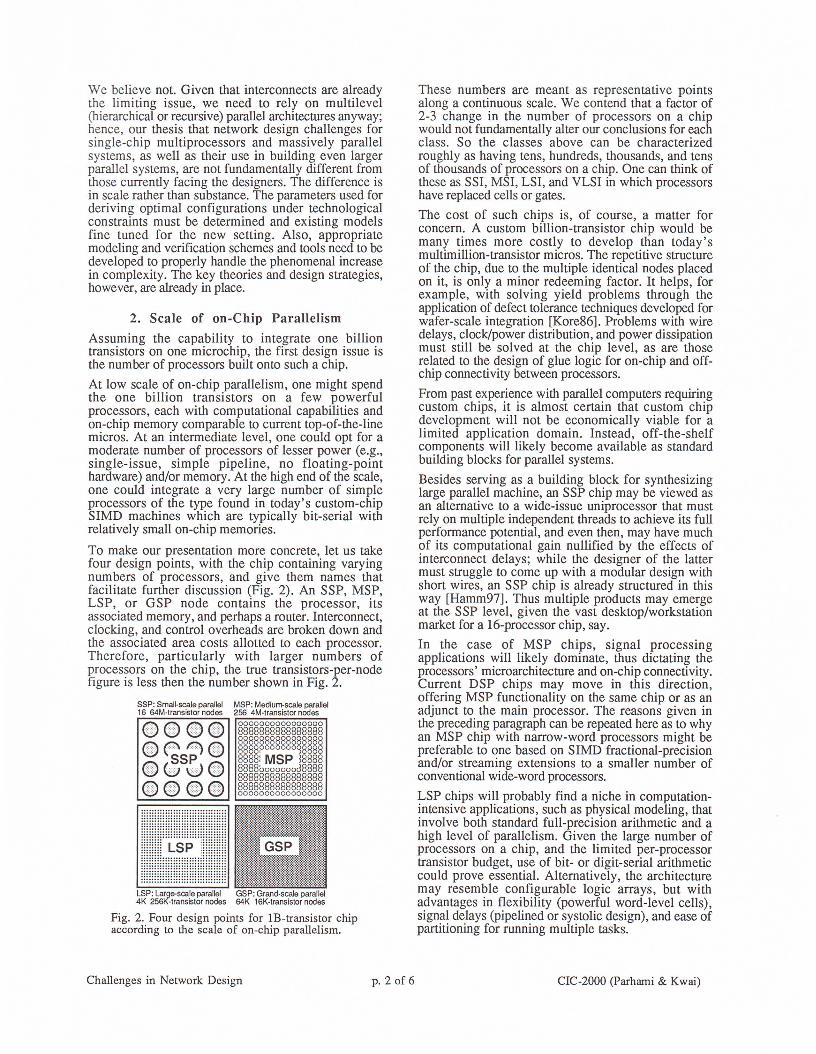
2. Scale of on-Chip ParallelismAssuming the capability to integrate one billiontransistors on one microchip, the first design issue isthe number of processors built onto such a chip.
At low scale of on-chip parallelism, one might spendthe one billion transistors on a few powerfulprocessors, each with computational capabilities andon-chip memory comparable to current top-of-the-linemicros. At an intermediate level, one could opt for amoderate number of processors of lesser power (e.g.,single-issue, simple pipeline, no floating-pointhardware) and/or memory. At the high end of the scale,one could integrate a very large number of simpleprocessors of the type found in today's custom-chipSIMD machines which are typically bit-serial withrelatively small on-chip memories.
To make our presentation more concrete, let us takefour design points, with the chip containing varyingnumbers of processors, and give them names thatfacilitate further discussion (Fig. 2). An SSP, MSP,LSP, or GSP node contains the processor, itsassociated memory, and perhaps a router. Interconnect,clocking, and control overheads are broken down andthe associated area costs allotted to each processor.Therefore, particularly with larger numbers ofprocessors on the chip, the true transistors-per-nodefigure is less then the number shown in Fig. 2.
SSP: Small-scale parallel16 64M-transistor nodes
11111111111111111111111111111111
:::::::r'LS'p''':::::::::!1!!!!!!IIIIIIIIIIIIIII!!!!!!!!!
LSP: Large-scale parallel4K 256K-transistor nodes 64K 16K-transistor nodes
Fig. 2. Four design points for lB-transistor chipaccording to the scale of on-chip parallelism.
Challenges in Network Design
These numbers are meant as representative pointsalong a continuous scale. We contend that a factor of2-3 change in the number of processors on a chipwould not fundamentally alter our conclusions for eachclass. So the classes above can be characterizedroughly as having tens, hundreds, thousands, and tensof thousands of processors on a chip. One can think ofthese as SSI, MSI, LSI, and VLSI in which processorshave replaced cells or gates.
The cost of such chips is, of course, a matter forconcern. A custom billion-transistor chip would bemany times more costly to develop than today'smultimillion-transistor micros. The repetitive structureof the chip, due to the mUltiple identical nodes placedon it, is only a minor redeeming factor. It helps, forexample, with solving yield problems through theapplication of defect tolerance techniques developed forwafer-scale integration [Kore86]. Problems with wiredelays, clock/power distribution, and power dissipationmust still be solved at the chip level, as are thoserelated to the design of glue logic for on-chip and off-chip connectivity between processors.
From past experience with parallel computers requiringcustom chips, it is almost certain that custom chipdevelopment will not be economically viable for alimited application domain. Instead, off-the-shelfcomponents will likely become available as standardbuilding blocks for parallel systems.
Besides serving as a building block for synthesizinglarge parallel machine, an SSP chip may be viewed asan alternative to a wide-issue uniprocessor that mustrely on multiple independent threads to achieve its fullperformance potential, and even then, may have muchof its computational gain nullified by the effects ofinterconnect delays; while the designer of the lattermust struggle to come up with a modular design withshort wires, an SSP chip is already structured in thisway [Hamm97]. Thus multiple products may emergeat the SSP level, given the vast desktop/workstationmarket for a 16-processor chip, say.
In the case of MSP chips, signal processingapplications will likely dominate, thus dictating theprocessors' microarchitecture and on-chip connectivity.Current DSP chips may move in this direction,offering MSP functionality on the same chip or as anadjunct to the main processor. The reasons given inthe preceding paragraph can be repeated here as to whyan MSP chip with narrow-word processors might bepreferable to one based on SIMD fractional-precisionand/or streaming extensions to a smaller number ofconventional wide-word processors.
LSP chips will probably find a niche in computation-intensive applications, such as physical modeling, thatinvolve both standard full-precision arithmetic and ahigh level of parallelism. Given the large number ofprocessors on a chip, and the limited per-processortransistor budget, use of bit- or digit-serial arithmeticcould prove essential. Alternatively, the architecturemay resemble configurable logic arrays, but withadvantages in flexibility (powerful word-level cells),signal delays (pipelined or systolic design), and ease ofpartitioning for running multiple tasks.
p. 2 of 6 CIC-2000 (Parhami & Kwai)
Behrooz Parhami
Text Box
242
Given its extremely simple processors with limitedmemory, a GSP chip is conceptually quite close toprocessor-in-memory (PIM) architectures [Gokh95]that integrate the processors into the memory accesslogic to alleviate the memory bandwidth bottleneck.The need for "intelligent" memories [Kozy97] has beencontemplated for several decades, ever since earlyassociative memories were proposed. The billion-transistor-chip capability might be just what is neededto end the tyranny of "dumb" DRAMs. Commoditymemory products with integrated processing powerwill be quite attractive, once we agree on thecapabilities that must be built in.
Of course, many hybrid solutions are also possible.For example, a chip may contain eight powerfulprocessors of the SSP variety, as well as 32K verysimple ones of the type discussed under GSP. We willnot consider such combinations any further.
3. Dominance of Wire DelaysOn-chip interconnects comprise local and global wiresthat link circuit elements and distribute power supplyand clock inputs. Downward scaling of VLSItechnologies continuously improves device switchingor computation times. The effect of this scaling oninterconnect performance, however, can be just theopposite, given the increased current density, chip size,and noise margin, along with reduced width andspacing. Short-term solutions to the interconnect delayproblem [Sylv99] will not scale indefinitely and areeven now inapplicable to global wiring.
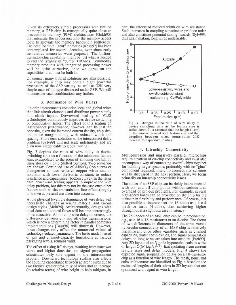
Fig. 3 depicts the ratio of wire delay to deviceswitching time as a function of the minimum featuresize, extrapolated to the point of allowing one billiontransistors on a chip (dotted portion). Two scenariosare shown: Continued use of AI/Si02 (top curve) orchangeover to less resistive copper wires and aninsulator with lower dielectric constant, to reduceresistance and capacitance (bottom curve). In the lattercase, downward scaling appears to improve the wiredelay problem, but this may not be the case once otherfactors such as the transmission line effect (largelyunknown at present) are taken into account.
At the physical level, the dominance of wire delay willnecessitate changes in wiring material and circuitdesign styles [Mein96]. Architecturally, designs withlocal data and control flows will become increasinglymore attractive. As on-chip wire delays increase, thedifference between on- and off-chip transmissions,which is now a determining factor in parallel computerimplementations [Basa96] will diminish. However,these changes only affect the numerical values oftechnology-related parameters. The basic model, basedon pin and channel-capacity limitations at variouspackaging levels, remains valid.
The effect of rising RC delays, resulting from narrowerwires and higher densities, on signal propagationconstitutes only one aspect of the interconnectproblem. Downward technology scaling also affectsthe coupling capacitance between adjacent wires due totwo factors: greater proximity of wires and an increase(in relative terms) of wire height to help mitigate, in
Challenges in Network Design
part, the effects of reduced width on wire resistance.Such increases in coupling capacitance produce noiseand also constitute potential timing hazards [Sylv99],thus again making long wires undesirable.8,---------------------~~,e
II
"I
Q)
E..."0>7.S.cu.~(/)6.8iUQi
~5.~'0.~ 4a:
·······0Lower-resistivity wires andlow-dielectric-constantinsulator; e.g. Cu/Polyimide
Fig. 3. Changes in the ratio of wire delay todevice switching time as the feature size isscaled down. It is assumed that the length (1 cm)of the wire is reduced with feature size and thatcoupling between wires contributes 20%increase to capacitive loading.
4. Intrachip ConnectivityMultiprocessor and massively parallel microchipsrequire a pattern of on-chip connectivity and must alsoencompass a way of connecting several chips togetherfor building larger systems, preferably with no "glue"component required. Interchip connectivity schemeswill be discussed in the next section. Here, we focusprimarily on intrachip connectivity issues.
The nodes of an SSP chip can be richly interconnectedwith on- and off-chip points without serious areaoverhead or pin-out problems. For example, severalhigh-speed buses can be provided on the chip for theultimate in flexibility and performance. Of course, it isalso possible to interconnect the 16 nodes as a 4 x 4mesh or torus (4-cube), thus achieving higherthroughput at a slight increase in latency.
The 256 nodes of an MSP chip can be interconnected,e.g., as a 16 x 16 mesh/torus or an 8-cube. The factorof two difference in diameters of the torus versushypercube connectivity of an MSP chip is relativelyinsignificant once other variables such as channelcapacities, router complexities, and signal propagationdelays on long wires are taken into account [Parh99].Any 2D layout of an N-node hypercube leads to wiresof length O((N log N)1/2). Extrapolating from currentfeature sizes and delay models, Fig. 4 shows theexpected signal propagation delays on alB-transistorchip as a function of wire length. The mesh, torus, andcube architectures are identified on Fig. 4 based on theestimated lengths of their wires in 2D layouts that areoptimized with regard to wire length.
p. 3 of 6 CIC-2000 (Parhami & Kwai)
Behrooz Parhami
Text Box
243

The significant propagation delay penalty associatedwith the 8-cube makes the torus (or even mesh)connectivity quite competitive, especially when therelative ease of connecting I/O ports to its 60 boundaryprocessors, or a subset thereof, is taken into account.Intermediate architectures between the preceding two(e.g., a 4-ary 4-cube) will likely not be attractive inview of added algorithmic complexity or cost overmesh/torus, without a noteworthy decrease in themaximum wire length over the hypercube. Similarly,richer connection schemes, with node degrees greaterthan eight, are unlikely to be cost effective.
2
2 4Wire length (mm)
Fig. 4. Intrachip wire delay as a function of wirelength. The use of copper wires and node layoutarea of 0.15 x 0.15 cm are assumed. For meshtopology, intraprocessor wire delays dominate.For torus, intra- and interprocessor wire delaysare comparable (folded layout). For hypercube,interprocessor delay is clearly dominant.
6o
As we shift our focus to an LSP chip, the importanceof network diameter starts to build up. A 64 x 64 torus(mesh) has a diameter of 64 (126) which can lead tosignificant delays. A 12-cube has a much smallerdiameter of 12, but besides needing more complexnodes of degree 12, its layout implies significant areaoverhead and signal propagation delays. Thus, weshould consider a hierarchical or recursive architectureon the chip to cope with diameter and long-wireproblems in much the same way as we now do formultichip/board MPPs [Yeh98].
One way to combine low diameter with simple layout,and thus shorter wires, is to apply systematic pruningto a dense network [Kwai99], [KwaiOO], [Parh99a].Fig. 5 [KwaiOO] exemplifies the layout area savingsthat can be obtained with pruning. For k-ary n-cubenetworks, pruning strategies are known that yieldnode-symmetric networks with substantially the samediameters as the unpruned networks. The negativeeffect of pruning on the bisection bandwidth is, at leastin part, mitigated by the use of wider channels madepossible through node degree reduction.
The often made assertion that network diameter is nolonger important, because we tend to use wormholerouting in modern parallel machines, is worth amention here. Even in the limited context of current
Challenges in Network Design
practice (no more than a few thousands of processors,wormhole switching, .and relatively long messages tomitigate the send/receive overheads), this assertion isdebatable [parhOO]. As we begin to seriously entertainthe notion of million-processor architectures [ClarOO],network topology once again assumes a crucial role.Finally, in the case of GSP, our options for on-chipconnectivity are quite limited. Given many thousandsof nodes on a chip, any increase in interconnectioncomplexity over a simple 256 x 256 mesh or torus islikely to consume so much of the chip area as to leavelittle real estate for the nodes' computing and storagefunctions. This can be self-defeating in that such anunderpowered node can do little before requiringcommunication with other nodes.
Use of configurable interconnects may offer someadvantages for GSP. With due care during the design,such configurable interconnects can serve the dualpurpose of yield enhancement and run-time setup ofefficient communication paths with relatively lowoverhead. By its nature, a GSP chip is more rigid than,say, an SSP chip, making its application domain morelimited. Thus, configurability can also be viewed asdesirable for mitigating the economic disadvantage thatcomes with narrow applicability.
It thus appears that on-chip connectivity problems forSSP and MSP are currently within our grasp; but LSPand GSP present certain challenges that must beconfronted with intensified research on interconnectionschemes and their VLSI layouts.
- r-- r-- - - roo-
0-+--+4-0·· .
0-+--+--+--0, ...
...0--+--+--+-0" ......<)--1....... ..0-+--+--+-0
. . . . .. . ,0--+--+--+-0" .. . ..... .. . .... 0--+--+--+-<> ..
....
.,,'
(a).c- r-- r-- roo-
~ n
l '\ ((')... -C O. ..(')
'-- '-- - - '-- -(b)
Fig. 5. The effect of pruning on network layoutarea complexity. (a) Folded layout of a 2D torus,with links to be pruned depicted as dotted lines.(b) More compact layout for the pruned torus.
p. 4 of 6 CIC-2000 (Parhami & Kwai)
Behrooz Parhami
Text Box
244
5. Interchip ArchitectureGiven a particular on-chip connectivity, two issuesmust be considered for building larger parallel systems.The first of these, the provision of off-chip links, isreally within the chip design realm. However, onemust look at the potential overall architectures in orderto decide on suitable off-chip connectivity. Perhaps themost general and flexible option is to provide one (or ahandful of) off-chip port(s) per processor. This isfeasible for SSP chips and workable, with serial ortime-shared ports, for MSP. However, such ports willsuffer from the double penalty of off-chip propagationdelays and long on-chip wires.
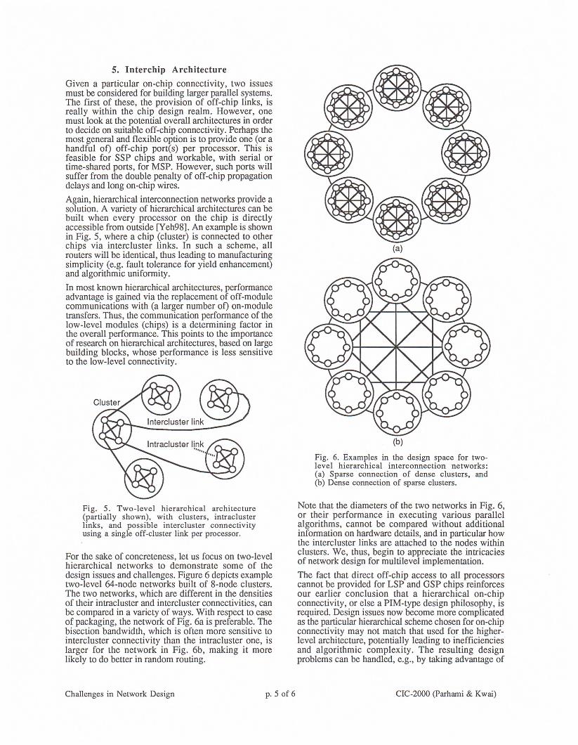
Again, hierarchical interconnection networks provide asolution. A variety of hierarchical architectures can bebuilt when every processor on the chip is directlyaccessible from outside [Yeh98]. An example is shownin Fig. 5, where a chip (cluster) is connected to otherchips via intercluster links. In such a scheme, allrouters will be identical, thus leading to manufacturingsimplicity (e.g. fault tolerance for yield enhancement)and algorithmic uniformity.
In most known hierarchical architectures, performanceadvantage is gained via the replacement of off-modulecommunications with (a larger number of) on-moduletransfers. Thus, the communication performance of thelow-level modules (chips) is a determining factor inthe overall performance. This points to the importanceof research on hierarchical architectures, based on largebuilding blocks, whose performance is less sensitiveto the low-level connectivity.
Fig. 5. Two-level hierarchical architecture(partially shown), with clusters, intraclusterlinks, and possible intercluster connectivityusing a single off-cluster link per processor.
For the sake of concreteness, let us focus on two-levelhierarchical networks to demonstrate some of thedesign issues and challenges. Figure 6 depicts exampletwo-level 64-node networks built of 8-node clusters.The two networks, which are different in the densitiesof their intracluster and intercluster connectivities, canbe compared in a variety of ways. With respect to easeof packaging, the network of Fig. 6a is preferable. Thebisection bandwidth, which is often more sensitive tointercluster connectivity than the intracluster one, islarger for the network in Fig. 6b, making it morelikely to do better in random routing.
Challenges in Network Design p. 5 of 6
(a)
(b)
Fig. 6. Examples in the design space for two-level hierarchical interconnection networks:(a) Sparse connection of dense clusters, and(b) Dense connection of sparse clusters.
Note that the diameters of the two networks in Fig. 6,or their performance in executing various parallelalgorithms, cannot be compared without additionalinformation on hardware details, and in particular howthe intercluster links are attached to the nodes withinclusters. We, thus, begin to appreciate the intricaciesof network design for multilevel implementation.
The fact that direct off-chip access to all processorscannot be provided for LSP and GSP chips reinforcesour earlier conclusion that a hierarchical on-chipconnectivity, or else a PIM-type design philosophy, isrequired. Design issues now become more complicatedas the particular hierarchical scheme chosen for on-chipconnectivity may not match that used for the higher-level architecture, potentially leading to inefficienciesand algorithmic complexity. The resulting designproblems can be handled, e.g., by taking advantage of
CIC-2000 (Parhami & Kwai)
Behrooz Parhami
Text Box
245

techniques for parallel system implementation usingboth hierarchical and recursive compositions [Yeh98].
Even though different connectivities can be combinedin an ad hoc manner to build a multilevel network, itwould be better from the viewpoint of algorithmicsimplicity, as well as ease of design and analysis, toapply a uniform design scheme that determines thenode connectivity rules in such a way that modularityis automatically ensured. This would lead to simplerrouting and computational algorithms that do not needto keep track of the level of hierarchy in order to adjusttheir behaviors accordingly.
The foregoing desirable property can be ascertainedthrough the use of index-permutation graphs [YehOO].As a unified model of hierarchical networks, index-permutation graphs allow us to modify networkstructure and capabilities via suitable adjustments innetwork components (nuclei), connectivity rules(generators or supergenerators), and other parameters.
To summarize, known design methods for hierarchicalinterconnection networks must be extended and refinedto allow systematic cost-performance tradeoffs duringthe design process of large systems employing parallelmicrochips. Whereas off-chip connectivity decisionsfor SSP and MSP can be handled with ad hoc methods,the use of a common design methodology is beneficialeven in these latter cases.
6. ConclusionAs these words are being written, the state of availablecomputational power can be summarized as follows:GFLOPS on desktop, TFLOPS in supercomputercenter, PFLOPS on drawing board. The foregoingprefixes used to be M, G, and T a little over a decadeago, and we almost routinely expect them to becomeT, P, and H (?) early in the next decade, if not sooner.However, it is almost certain that the latter transitionwill not occur solely by improving the architecturalmethods that fueled the growth of computationalpower in the 1980s and 1990s.
Emergence of mUltiprocessor and massively parallelmicrochips are expected to help in this regard. We donot see any insurmountable problem in building andutilizing multiprocessor or massively parallel chipscontaining of the order of one billion transistors.Multiprocessor chips, already a reality, will enhancethe capabilities of future workstations as well asprovide building blocks for higher performancesystems. With massively parallel microchips,multimillion-processor MPPs no longer constitute anunrealizable or unaffordable dream.
Emerging research results on the synthesis of parallelarchitectures under propagation delay, channel capacity,and packaging constraints, when suitably modified totake the new physical and technological parametersinto consideration, can lead to the solution ofanticipated design problems. Optimal operating pointswith regard to system partitioning and interconnectionstructure may change, but the models and know-howfor dealing with the most fundamental design problemsare already in place.
Challenges in Network Design
References[Abra91] Abraham, S. and K. Padrnanabhan, "Performance
of Multicomputer Networks under Pin-out Constraints",1. Parallel and Distributed Computing, Vol. 12,pp. 237-248, July 1991.
[Bald96] Baldi, L., "Industry Roadrnaps: The Challenge ofComplexity", Microelectronic Engineering, Vor. 34,No.1, pp. 9-26, Dec. 1996.
[Basa96J Basak, D. and D.K. Panda, "Designing ClusteredMultiprocessor Systems under Packaging andTechnological Advancements", IEEE Trans. Parallel andDistributed Systems, Vol. 7, pp. 962-978, Sep. 1996.
[Burg96] Burger, D., J.R. Goodman, and A. Kagi,"Quantifying Memory Bandwidth Limitations ofCurrent and Future Microprocessors", Proc. Int'l Symp.Computer Architecture, May 1996, pp. 78-89.
[ClarOO] Clark, D., "Blue Gene and the Race TowardPetaflops CajJacity", IEEE Concurrency, Vol. 8,pp. 5-9, Jan.-Mar. 2000.
[Gokh95] Gokhale, M., B. Holmes, and K. Iobst,"Processing in Memory: The Terasys MassivelyParallel PIM Array", IEEE Computer, Vol. 28,pp. 23-31, Apr. 1995.
[Hamm97] Hammond, L., B.A. Nayfeh, and K. Olukotun,"A Single-Chip Multiprocessor", IEEE Computer,Vol. 30, pp. 79-85, Sep. 1997.
[Kore86] Koren, I. and D.K. Pradhan, "Yield andPerformance Enhancement Through Redundancy inVLSI and WSI Multiprocessor Systems", Proceedings ofthe IEEE, Vol. 74, pp. 699-711, May 1986.
[Kozy97] Koz)'fakis, C.E. et aI, "Scalable Processors inthe Billion-Transistor Era: IRAM", IEEE Computer,Vol. 30, pp. 79-85, Sep. 1997.
[Kwai99] Kwai, D.M. and B. Parhami, "Comp_aring Torus,Pruned Torus, and Manhattan Street Networks asInterconnection Architectures for Highly ParallelComputers", Proc. In!' I Cont Parallel and DistributedComputing and Systems, Nov. 1999, pp. 19-22.
[KwaiOOl Kwai, D.-M. and B. Parhami, "A UnifiedFormulation of Honeycomb and Diamond Networks",IEEE Trans. Parallel and Distributed Systems, to appear.
[Mein96] Meindl, J.D., "Gigascale Integration: Is the Skythe Limit?", IEEE Circuits and Devices, Vol. 12, No.6,pp. 19-23 & 32, Nov. 1996.
[Oluk96] Olukotun, K., B.A. Nayfeh, L. Hammond, K.Wilson, and K. Chang, "The Case for a Single-ChipMUltiprocessor", Proc. Int'I Symp. ArchllecturalSupport for Programming Languages and OperatingSystems, Oct. 1996, pp. 2-11.
[Parh95] Parhami, B., "Panel Assesses SIMD's Future",IEEE Computer, Vol. 28, pp. 89-91, June 1995.Extended version: www.ece.ucsb.edu/faculty/parhami
[Parh99] Parhami, B., Introduction to Parallel Processing:Algorithms and Architectures, Plenum Press, 1999.
[Parh99a] Parhami, B. and D.-M. Kwai, "PeriodicallyRegular Chordal Rings", IEEE Trans. Parallel andDistributed Systems, Vol. 10, pp. 658-672, June 1999.
[ParhOO] Parhami, B. and C.-H. Yeh, "Why NetworkDiameter is Still Important", these Proceedings.
[Sylv99] Sylvester, D. and K. Keutzer, "Rethinking Deep-Submicron Circuit Design", IEEE Computer, Vol. 32,pp. 25-33, Nov. 1999.
[Wain97] Waingold, E. et aI, "Baring It All to Software:Raw Machines", IEEE Computer, Vol. 30, pp. 86-93,Sep. 1997.
[Yeh98] Yeh, C.-H. and B. Parhami, "Synthesizing High-Performance Parallel Architectures under Inter-ModuleBandwidth Constraints", Proc. In!' I Cont Paralleland Distributed Computing and Systems, Oct. 1998,pp. 414-416.
[YehOO] Yeh, C.-H. and B. Parhami, "A Unified Model forHierarchical Networks Based on an Extension of CayleyGraphs", IEEE Trans. Parallel and Distributed Systems,to appear.
p. 6 of 6 crC-2000 (Parhami & Kwai)
Behrooz Parhami
Text Box
246