Challenges in Implementing DDR3
22
© 2008 Altera Corporation—Public Challenges in Implementing DDR3 Challenges in Implementing DDR3 Memory Interface on PCB Systems Memory Interface on PCB Systems - - A A Methodology for Interfacing DDR3 Methodology for Interfacing DDR3 SDRAM DIMM to an FPGA SDRAM DIMM to an FPGA
-
Upload
bharat-g-hegde -
Category
Documents
-
view
33 -
download
2
description
ddr3 notes
Transcript of Challenges in Implementing DDR3
© 2008 Altera Corporation—Public
Challenges in Implementing DDR3 Challenges in Implementing DDR3
Memory Interface on PCB Systems Memory Interface on PCB Systems -- A A
Methodology for Interfacing DDR3 Methodology for Interfacing DDR3
SDRAM DIMM to an FPGASDRAM DIMM to an FPGA
2
© 2008 Altera Corporation—Public
Altera, Stratix, Arria, Cyclone, MAX, HardCopy, Nios, Quartus, and MegaCore are trademarks of Altera Corporation
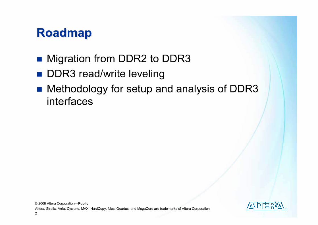
RoadmapRoadmap
� Migration from DDR2 to DDR3
� DDR3 read/write leveling
� Methodology for setup and analysis of DDR3
interfaces
3
© 2008 Altera Corporation—Public
Altera, Stratix, Arria, Cyclone, MAX, HardCopy, Nios, Quartus, and MegaCore are trademarks of Altera Corporation
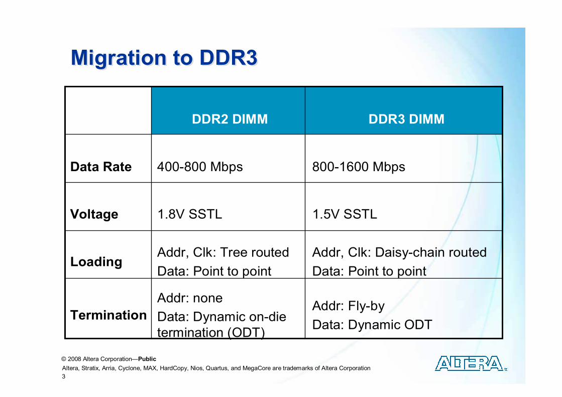
Migration to DDR3Migration to DDR3
Addr: none
Data: Dynamic on-die
termination (ODT)
Addr, Clk: Tree routed
Data: Point to point
1.8V SSTL
400-800 Mbps
DDR2 DIMM
Addr: Fly-by
Data: Dynamic ODT Termination
Addr, Clk: Daisy-chain routed
Data: Point to pointLoading
1.5V SSTLVoltage
800-1600 MbpsData Rate
DDR3 DIMM
4
© 2008 Altera Corporation—Public
Altera, Stratix, Arria, Cyclone, MAX, HardCopy, Nios, Quartus, and MegaCore are trademarks of Altera Corporation
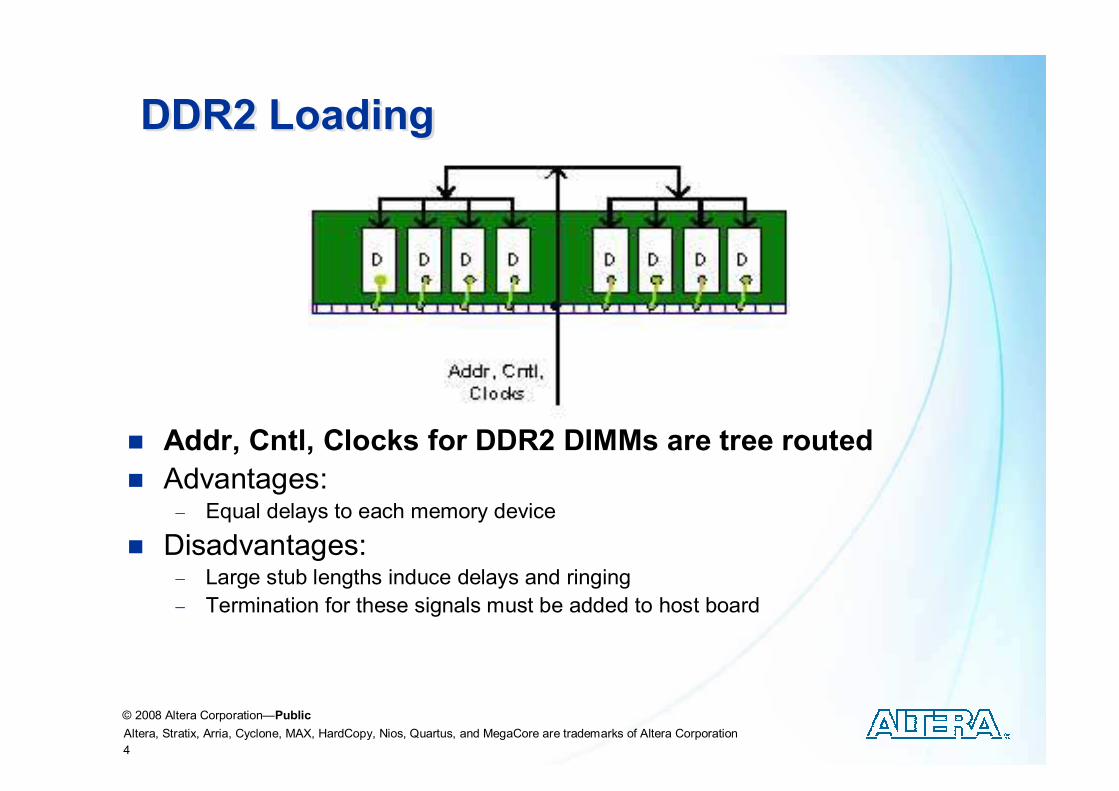
DDR2 LoadingDDR2 Loading
� Addr, Cntl, Clocks for DDR2 DIMMs are tree routed
� Advantages: − Equal delays to each memory device
� Disadvantages:− Large stub lengths induce delays and ringing
− Termination for these signals must be added to host board
5
© 2008 Altera Corporation—Public
Altera, Stratix, Arria, Cyclone, MAX, HardCopy, Nios, Quartus, and MegaCore are trademarks of Altera Corporation
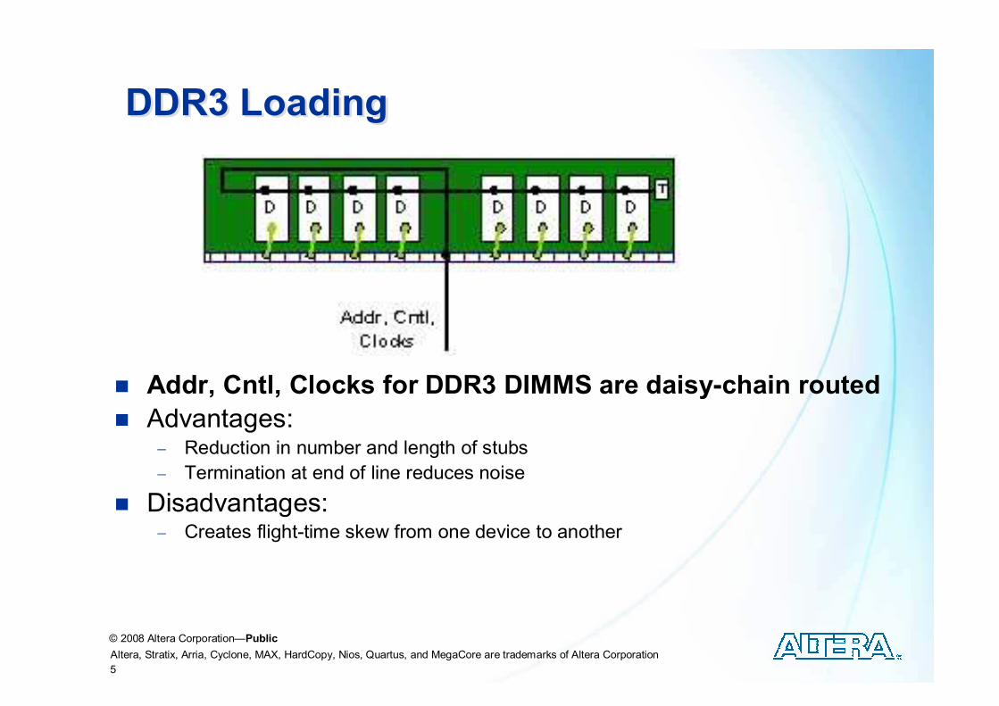
DDR3 LoadingDDR3 Loading
� Addr, Cntl, Clocks for DDR3 DIMMS are daisy-chain routed
� Advantages: − Reduction in number and length of stubs
− Termination at end of line reduces noise
� Disadvantages:− Creates flight-time skew from one device to another
6
© 2008 Altera Corporation—Public
Altera, Stratix, Arria, Cyclone, MAX, HardCopy, Nios, Quartus, and MegaCore are trademarks of Altera Corporation
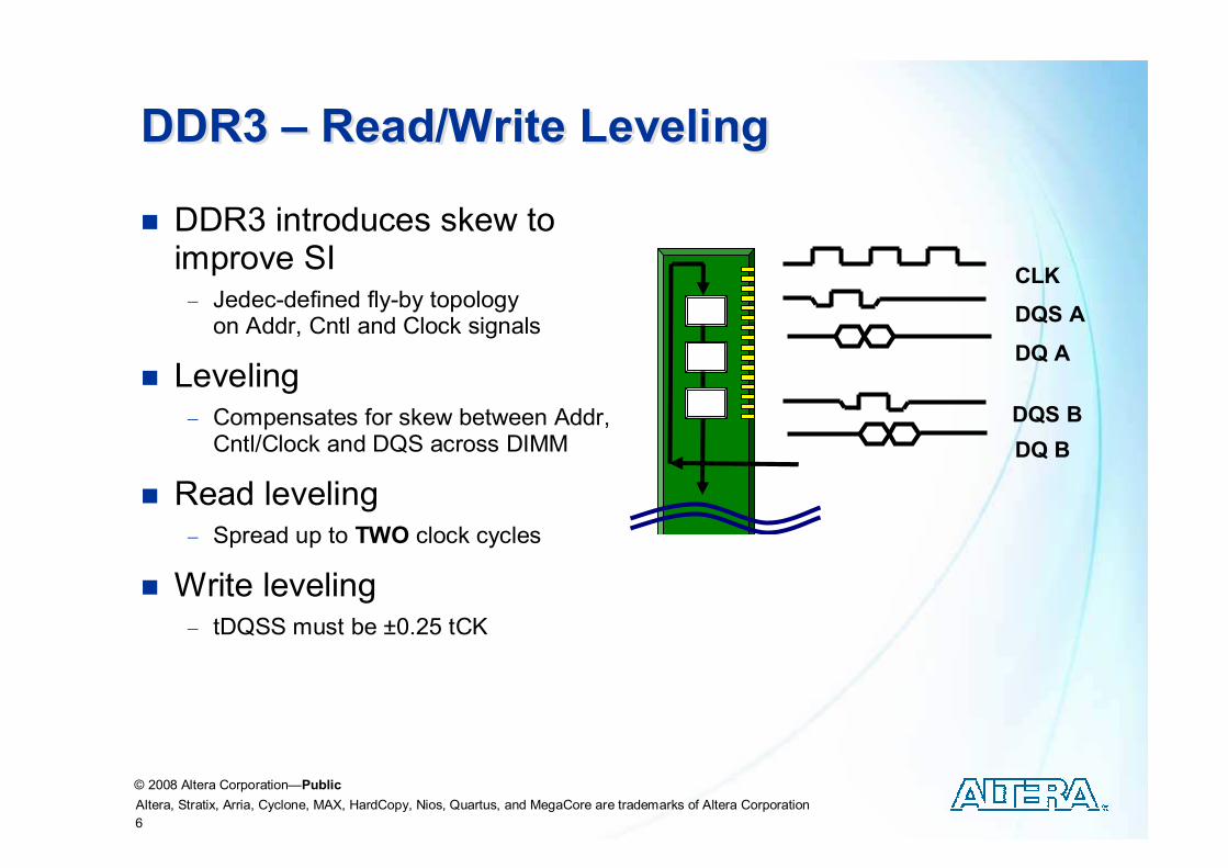
DDR3 – Read/Write LevelingDDR3 – Read/Write Leveling
� DDR3 introduces skew to improve SI − Jedec-defined fly-by topology on Addr, Cntl and Clock signals
� Leveling − Compensates for skew between Addr, Cntl/Clock and DQS across DIMM
� Read leveling− Spread up to TWO clock cycles
� Write leveling− tDQSS must be ±0.25 tCK
CLK
DQS A
DQ A
DQS B
DQ B
7
© 2008 Altera Corporation—Public
Altera, Stratix, Arria, Cyclone, MAX, HardCopy, Nios, Quartus, and MegaCore are trademarks of Altera Corporation
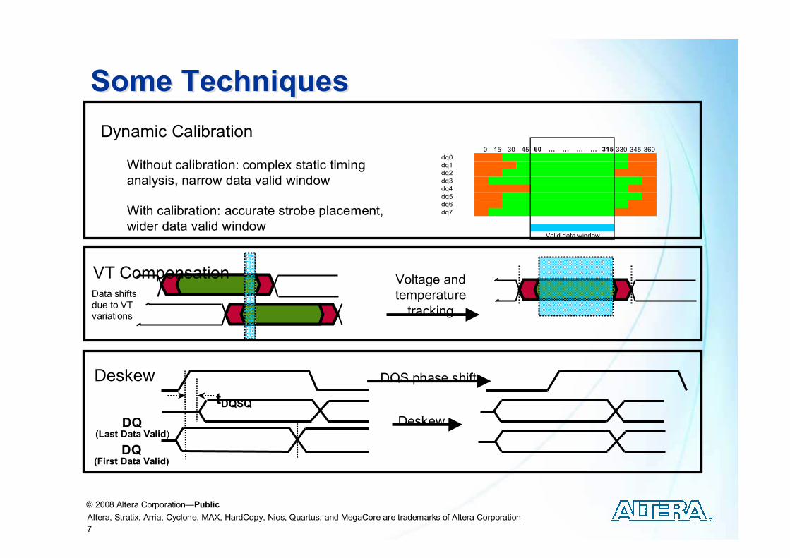
Some TechniquesSome Techniques
With calibration: accurate strobe placement,
wider data valid window
DQ(Last Data Valid)
DQ(First Data Valid)
tDQSQ
DQS phase shift
Deskew
Voltage and
temperature
tracking
Data shifts
due to VT
variations
0 15 30 45 60 … … … … 315 330 345 360
dq0
dq1
dq2
dq3
dq4
dq5
dq6
dq7
Valid data window
Without calibration: complex static timing
analysis, narrow data valid window
Dynamic Calibration
VT Compensation
Deskew
8
© 2008 Altera Corporation—Public
Altera, Stratix, Arria, Cyclone, MAX, HardCopy, Nios, Quartus, and MegaCore are trademarks of Altera Corporation
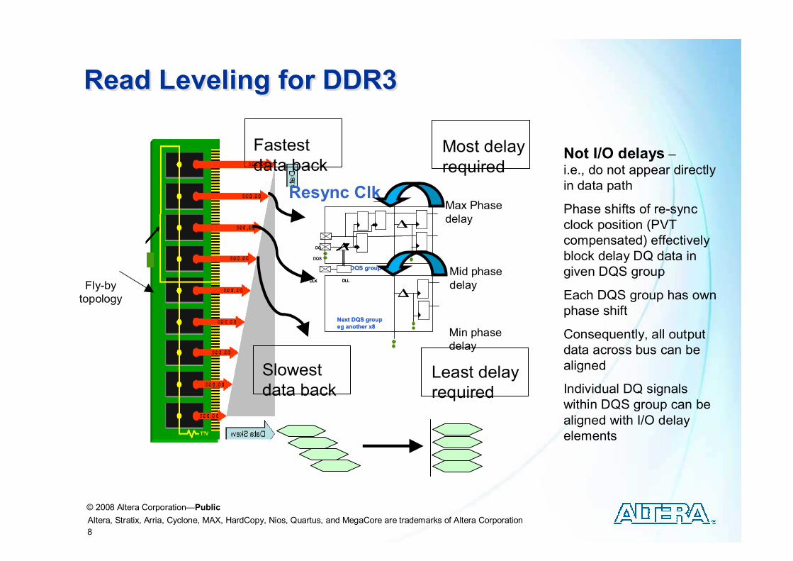
Read Leveling for DDR3Read Leveling for DDR3
DLLCLK
DQS
DQ
Next DQS group
eg another x8
DQS group eg x8
DLLCLK DLLCLK
DQS
DQ
Next DQS group
eg another x8
DQS group eg x8
Resync ClkMax Phase
delay
Mid phase
delay
Not I/O delays –i.e., do not appear directly
in data path
Phase shifts of re-sync
clock position (PVT
compensated) effectively
block delay DQ data in
given DQS group
Each DQS group has own
phase shift
Consequently, all output
data across bus can be
aligned
Individual DQ signals
within DQS group can be
aligned with I/O delay
elements
Fastest
data backMost delay
required
Slowest
data backLeast delay
required
Min phase
delay
Fly-by
topology
9
© 2008 Altera Corporation—Public
Altera, Stratix, Arria, Cyclone, MAX, HardCopy, Nios, Quartus, and MegaCore are trademarks of Altera Corporation
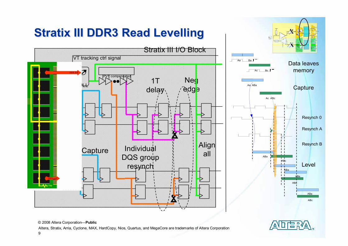
Stratix III DDR3 Read LevellingStratix III DDR3 Read Levelling
DLL
(PVT compensation)
90°90°
Aa Ba
Ac Bc
Aa ABa
Ac ABc
ABa
ABc
ABa
ABc
ABa
ABa
ABc
Stratix III I/O Block
Capture
1T
delay
Neg
edge Capture
Data leaves
memory
Individual
DQS group
resynch
Resynch 0
Resynch A
Resynch BAlign
all
Level
PLL
PVT compensated
VT tracking ctrl signal
10
© 2008 Altera Corporation—Public
Altera, Stratix, Arria, Cyclone, MAX, HardCopy, Nios, Quartus, and MegaCore are trademarks of Altera Corporation
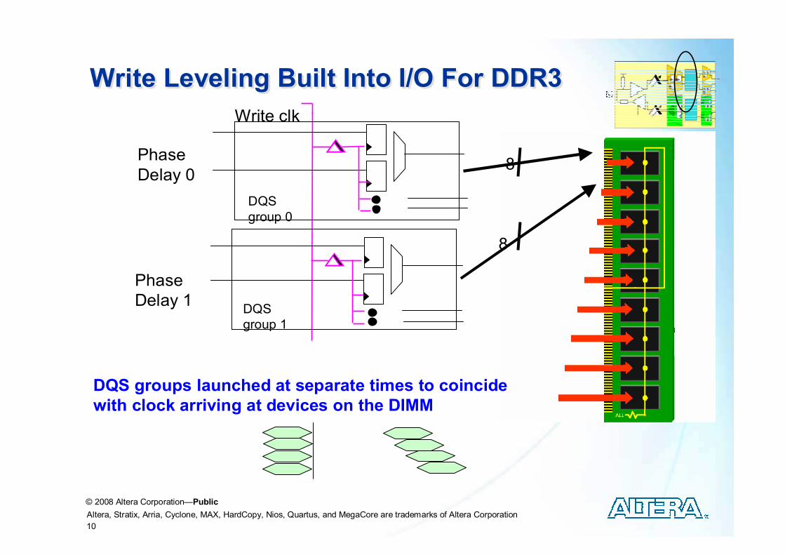
Write Leveling Built Into I/O For DDR3Write Leveling Built Into I/O For DDR3
DQS groups launched at separate times to coincide
with clock arriving at devices on the DIMM
8
8
Write clk
DQS
group 1
DQS
group 0
Phase
Delay 0
Phase
Delay 1
11
© 2008 Altera Corporation—Public
Altera, Stratix, Arria, Cyclone, MAX, HardCopy, Nios, Quartus, and MegaCore are trademarks of Altera Corporation
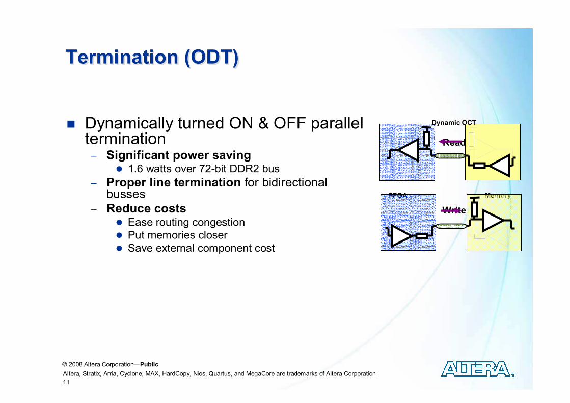
Termination (ODT)Termination (ODT)
� Dynamically turned ON & OFF parallel termination − Significant power saving
� 1.6 watts over 72-bit DDR2 bus
− Proper line termination for bidirectional busses
− Reduce costs� Ease routing congestion
� Put memories closer
� Save external component cost
Write
FPGA Memory
Read
Dynamic OCT
12
© 2008 Altera Corporation—Public
Altera, Stratix, Arria, Cyclone, MAX, HardCopy, Nios, Quartus, and MegaCore are trademarks of Altera Corporation
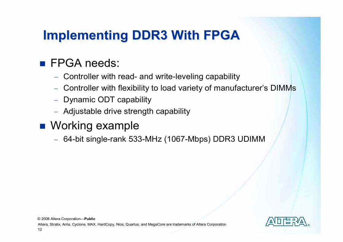
Implementing DDR3 With FPGAImplementing DDR3 With FPGA
� FPGA needs:− Controller with read- and write-leveling capability
− Controller with flexibility to load variety of manufacturer’s DIMMs
− Dynamic ODT capability
− Adjustable drive strength capability
� Working example− 64-bit single-rank 533-MHz (1067-Mbps) DDR3 UDIMM
13
© 2008 Altera Corporation—Public
Altera, Stratix, Arria, Cyclone, MAX, HardCopy, Nios, Quartus, and MegaCore are trademarks of Altera Corporation
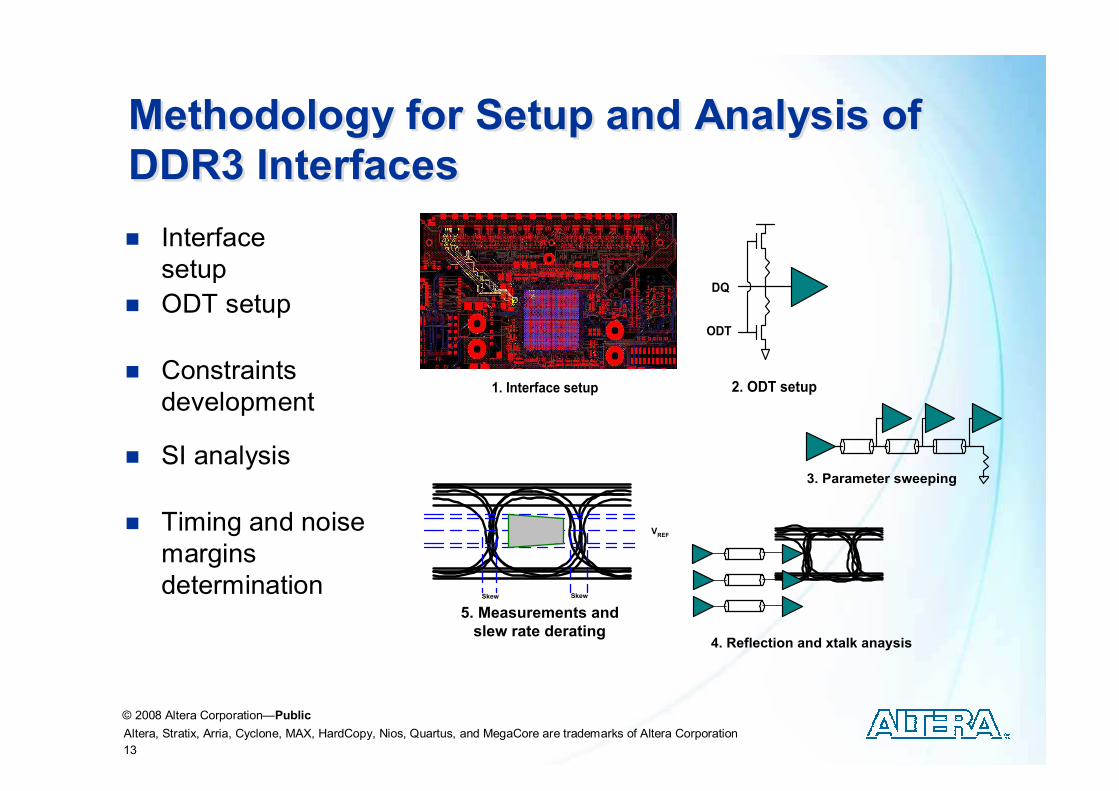
Methodology for Setup and Analysis of
DDR3 Interfaces
Methodology for Setup and Analysis of
DDR3 Interfaces
VREF
SkewSkew
5. Measurements and
slew rate derating4. Reflection and xtalk anaysis
3. Parameter sweeping
2. ODT setup
DQ
ODT
� ODT setup
� Constraints
development
� SI analysis
� Timing and noise
margins
determination
� Interface
setup
1. Interface setup
14
© 2008 Altera Corporation—Public
Altera, Stratix, Arria, Cyclone, MAX, HardCopy, Nios, Quartus, and MegaCore are trademarks of Altera Corporation
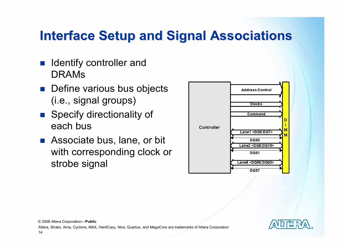
Interface Setup and Signal AssociationsInterface Setup and Signal Associations
� Identify controller and
DRAMs
� Define various bus objects
(i.e., signal groups)
� Specify directionality of
each bus
� Associate bus, lane, or bit
with corresponding clock or
strobe signal
15
© 2008 Altera Corporation—Public
Altera, Stratix, Arria, Cyclone, MAX, HardCopy, Nios, Quartus, and MegaCore are trademarks of Altera Corporation
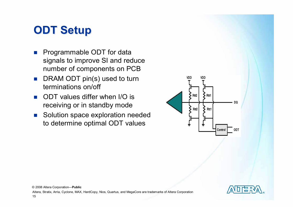
ODT SetupODT Setup
� Programmable ODT for data
signals to improve SI and reduce
number of components on PCB
� DRAM ODT pin(s) used to turn
terminations on/off
� ODT values differ when I/O is
receiving or in standby mode
� Solution space exploration needed
to determine optimal ODT values
16
© 2008 Altera Corporation—Public
Altera, Stratix, Arria, Cyclone, MAX, HardCopy, Nios, Quartus, and MegaCore are trademarks of Altera Corporation
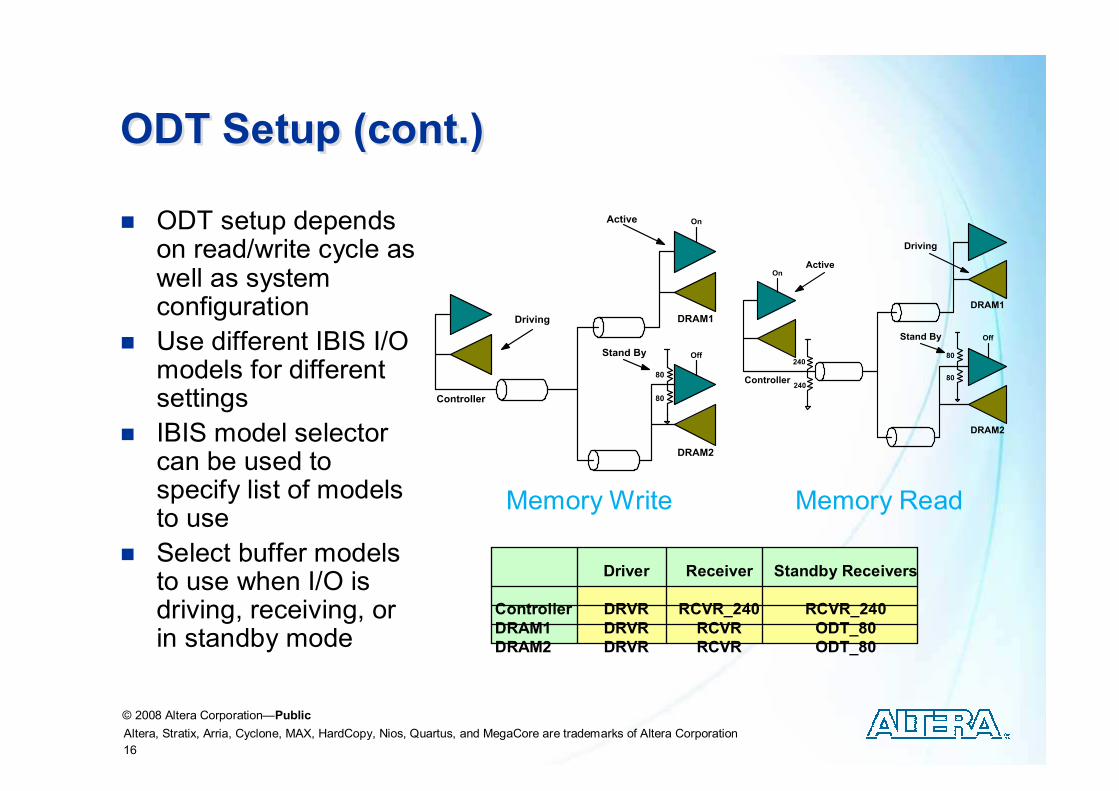
ODT Setup (cont.)ODT Setup (cont.)
� ODT setup depends on read/write cycle as well as system configuration
� Use different IBIS I/O models for different settings
� IBIS model selector can be used to specify list of models to use
� Select buffer models to use when I/O is driving, receiving, or in standby mode
Controller
DRAM1
DRAM2
Stand By
Driving
Active On
Off
80
80
Controller
DRAM1
DRAM2
Stand By
Driving
Active
Off
On
80
80
240
240
Memory Write Memory Read
ODT_80RCVRDRVRDRAM2
ODT_80RCVRDRVRDRAM1
RCVR_240RCVR_240DRVRController
Standby ReceiversReceiverDriver
17
© 2008 Altera Corporation—Public
Altera, Stratix, Arria, Cyclone, MAX, HardCopy, Nios, Quartus, and MegaCore are trademarks of Altera Corporation
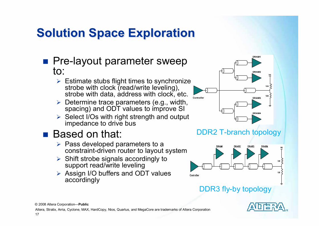
Solution Space ExplorationSolution Space Exploration
� Pre-layout parameter sweep to:� Estimate stubs flight times to synchronize strobe with clock (read/write leveling), strobe with data, address with clock, etc.
� Determine trace parameters (e.g., width, spacing) and ODT values to improve SI
� Select I/Os with right strength and output impedance to drive bus
� Based on that:� Pass developed parameters to a constraint-driven router to layout system
� Shift strobe signals accordingly to support read/write leveling
� Assign I/O buffers and ODT values accordingly
DDR2 T-branch topology
DDR3 fly-by topology
18
© 2008 Altera Corporation—Public
Altera, Stratix, Arria, Cyclone, MAX, HardCopy, Nios, Quartus, and MegaCore are trademarks of Altera Corporation
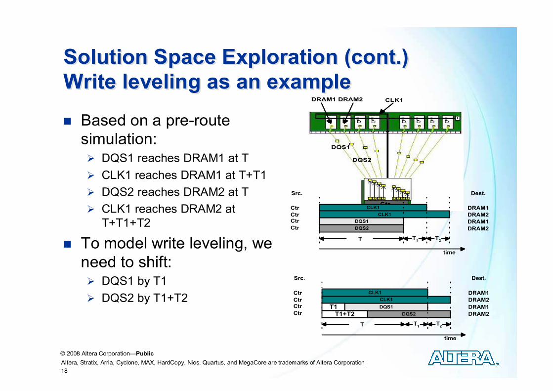
Solution Space Exploration (cont.)
Write leveling as an example
Solution Space Exploration (cont.)
Write leveling as an example
� Based on a pre-route
simulation:� DQS1 reaches DRAM1 at T
� CLK1 reaches DRAM1 at T+T1
� DQS2 reaches DRAM2 at T
� CLK1 reaches DRAM2 at
T+T1+T2
� To model write leveling, we
need to shift:� DQS1 by T1
� DQS2 by T1+T2
CLK1
DQS1
DQS2
Ctr
DRAM1 DRAM2
CLK1
DQS2
DQS1
CLK1
T T1
T2
Dest.Src.
Ctr
CtrCtr
Ctr DRAM2
DRAM1
DRAM2
DRAM1
time
CLK1
DQS2
DQS1
CLK1
T T1
T2
Dest.Src.
Ctr
CtrCtr
Ctr DRAM2
DRAM1
DRAM2
DRAM1
T1T1+T2
time
19
© 2008 Altera Corporation—Public
Altera, Stratix, Arria, Cyclone, MAX, HardCopy, Nios, Quartus, and MegaCore are trademarks of Altera Corporation
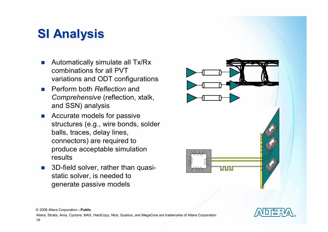
SI AnalysisSI Analysis
� Automatically simulate all Tx/Rx
combinations for all PVT
variations and ODT configurations
� Perform both Reflection and
Comprehensive (reflection, xtalk,
and SSN) analysis
� Accurate models for passive
structures (e.g., wire bonds, solder
balls, traces, delay lines,
connectors) are required to
produce acceptable simulation
results
� 3D-field solver, rather than quasi-
static solver, is needed to
generate passive models
20
© 2008 Altera Corporation—Public
Altera, Stratix, Arria, Cyclone, MAX, HardCopy, Nios, Quartus, and MegaCore are trademarks of Altera Corporation
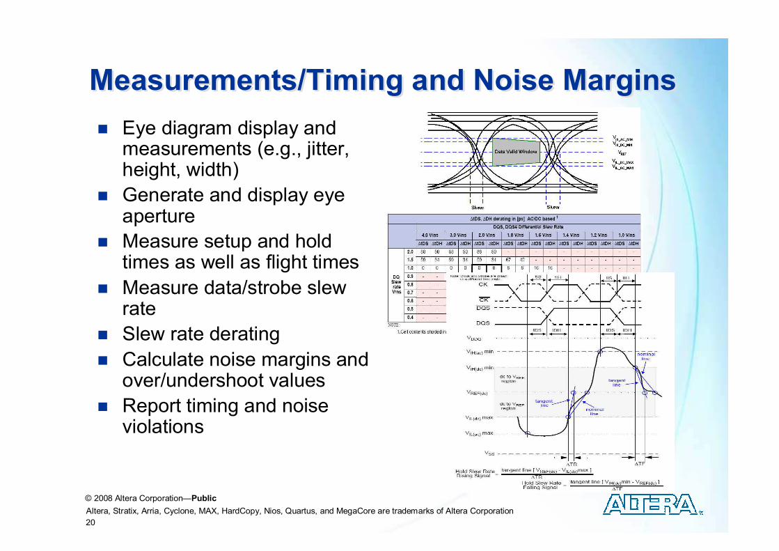
Measurements/Timing and Noise MarginsMeasurements/Timing and Noise Margins
� Eye diagram display and measurements (e.g., jitter, height, width)
� Generate and display eye aperture
� Measure setup and hold times as well as flight times
� Measure data/strobe slew rate
� Slew rate derating
� Calculate noise margins and over/undershoot values
� Report timing and noise violations
21
© 2008 Altera Corporation—Public
Altera, Stratix, Arria, Cyclone, MAX, HardCopy, Nios, Quartus, and MegaCore are trademarks of Altera Corporation
SummarySummary
� Discussed features and design challenges of
DDR3 interfaces
� Presented methodology to tackle various DDR3
design challenges
� Proposed methodology is easy to follow and
shortens design cycle

22
© 2008 Altera Corporation—Public
Altera, Stratix, Arria, Cyclone, MAX, HardCopy, Nios, Quartus, and MegaCore are trademarks of Altera Corporation
Questions Questions ??