Challenge to advanced laser materials processing in ...€¦RIKEN Review No.50(January, 2003):...
9
RIKEN Review No. 50 (January, 2003): Focused on Laser Precision Microfabrication (LPM 2002) Challenge to advanced laser materials processing in Japanese industry Isamu Miyamoto # Department of Manufacturing Science, Gradient School of Engineering, Osaka University Japan is one of the most advanced countries in manufacturing technology, and lasers have played an important role in the advancement of manufacturing technology in a variety of industrial fields. The contribution of laser materials processing to Japanese industry is significant for both macroprocessing and microprocessing. The present paper describes the recent trend and topics of industrial applications in terms of the hardware and the software in order to show how the Japanese industry is challenging in advanced materials processing using lasers, and national projects related to laser materials processing are also briefly introduced. 1. Introduction Lasers have greatly contributed to major fields of science as well as technologies since the first success in laser oscillation in 1960. There is no doubt that the laser is one of the great- est inventions of the 20th century. Particularly in materials processing, lasers have played an important role. The ad- vancement of the latest surgery, electronic devices, measuring instruments, automobiles, aircrafts, nuclear power generation and so on might have been vastly limited without laser ma- terials processing. Entering the 21st century, manufacturing technologies have become more and more reliant upon lasers, and there is no doubt lasers will continue to play an important role and be- come more valuable. The 21st century is indeed “the age of light ”. Japan is one of the most advanced countries in manu- facturing technology and lasers have been playing an impor- tant role. This article describes how the Japanese industry challenges in advanced materials processing using lasers for macro- to microprocessing in manufacturing technologies. 2. Lasers and peripherals 2.1 Development of all-solid-state high-power lasers A 5-year R&D national project, “Advanced Photon Process- ing and Measurement Technology”, started in March, 1997 in- volving 13 private companies, a university, and four research groups at the National Institute of Advanced Industrial Sci- ence and Technology. 1) This project has two R&D themes, “High-power all-solid-state laser” and “Tightly focusing all- solid-state laser” for developing solid-state lasers. The aim of the first theme is to develop high-power (10kW) LD-pumped lasers with a compact laser head of less than 0.05 m 3 volume using both rod- and slab-type Nd:YAG crys- tals for cutting and welding applications of heavy sections. A rod-type Nd:YAG laser composed of 6 modules was devel- oped with a CW (continuous wave) output of 12.0 kW at an optical conversion efficiency η=23%. A slab-type laser with an output of more than 10 kW was also developed. These # e-mail address: [email protected] technologies have been transferred to industry for the com- mercial LD-pumped Nd:YAG laser system. In the second theme, the aim is to develop tightly focusing all- solid-state laser technology for high-accuracy processing, and different types of lasers were developed. A high-brightness high repetition rate UV (ultraviolet) all-solid-state laser with an output power of 1 kW was attained at an efficiency of η=23 % by 4 modules, and can be focused into a diameter of 40µm. In this system, advanced CLBO crystals having higher laser-induced damage threshold were also developed. By using these crystals, a UV output of 42 W at 266 nm was attained with a stability of 100 h at 20 W. A disk-type 1 kW- fiber laser was also developed. 2.2 Development of line-narrowed F 2lasers The Association of Super-advanced Electronic Technologies (ASET) started a government-supported two-year project (see Section 4.3), “The F2 Laser Lithography Development Project ”, in 2000 to realizing F2 lithography technologies. 2) In this project, an average power output as high as 25 W is required for high throughput. In the F2 laser system, the spectral width depends on the optical system used in F2 lithography; catadioptric requires 1.2 pm, and dioptiric re- quires 0.5 pm for CaF2 +BaF2 lenses and 0.2 pm for all CaF2 lenses. A spectral width of 0.2 pm is required for lens systems using only CaF2, because BaF2 is not available now (Fig. 1). Fig. 1. Lens design and laser system for 157 nm lithography. 2) 20
Transcript of Challenge to advanced laser materials processing in ...€¦RIKEN Review No.50(January, 2003):...
RIKEN Review No. 50 (January, 2003): Focused on Laser Precision Microfabrication (LPM 2002)
Challenge to advanced laser materials processing inJapanese industry
Isamu Miyamoto#
Department of Manufacturing Science, Gradient School of Engineering, Osaka University
Japan is one of the most advanced countries in manufacturing technology, and lasers have played an importantrole in the advancement of manufacturing technology in a variety of industrial fields. The contribution oflaser materials processing to Japanese industry is significant for both macroprocessing and microprocessing.The present paper describes the recent trend and topics of industrial applications in terms of the hardwareand the software in order to show how the Japanese industry is challenging in advanced materials processingusing lasers, and national projects related to laser materials processing are also briefly introduced.
1. Introduction
Lasers have greatly contributed to major fields of science aswell as technologies since the first success in laser oscillationin 1960. There is no doubt that the laser is one of the great-est inventions of the 20th century. Particularly in materialsprocessing, lasers have played an important role. The ad-vancement of the latest surgery, electronic devices, measuringinstruments, automobiles, aircrafts, nuclear power generationand so on might have been vastly limited without laser ma-terials processing.
Entering the 21st century, manufacturing technologies havebecome more and more reliant upon lasers, and there is nodoubt lasers will continue to play an important role and be-come more valuable. The 21st century is indeed “the age oflight”. Japan is one of the most advanced countries in manu-facturing technology and lasers have been playing an impor-tant role. This article describes how the Japanese industrychallenges in advanced materials processing using lasers formacro- to microprocessing in manufacturing technologies.
2. Lasers and peripherals
2.1 Development of all-solid-state high-power lasersA 5-year R&D national project, “Advanced Photon Process-ing and Measurement Technology”, started in March, 1997 in-volving 13 private companies, a university, and four researchgroups at the National Institute of Advanced Industrial Sci-ence and Technology.1) This project has two R&D themes,“High-power all-solid-state laser” and “Tightly focusing all-solid-state laser” for developing solid-state lasers.
The aim of the first theme is to develop high-power (10kW)LD-pumped lasers with a compact laser head of less than0.05m3 volume using both rod- and slab-type Nd:YAG crys-tals for cutting and welding applications of heavy sections.A rod-type Nd:YAG laser composed of 6 modules was devel-oped with a CW (continuous wave) output of 12.0 kW at anoptical conversion efficiency η=23%. A slab-type laser withan output of more than 10 kW was also developed. These
# e-mail address: [email protected]
technologies have been transferred to industry for the com-mercial LD-pumped Nd:YAG laser system.
In the second theme, the aim is to develop tightly focusing all-solid-state laser technology for high-accuracy processing, anddifferent types of lasers were developed. A high-brightnesshigh repetition rate UV (ultraviolet) all-solid-state laser withan output power of 1 kW was attained at an efficiency ofη=23 % by 4 modules, and can be focused into a diameterof 40µm. In this system, advanced CLBO crystals havinghigher laser-induced damage threshold were also developed.By using these crystals, a UV output of 42W at 266 nm wasattained with a stability of 100 h at 20W. A disk-type 1 kW-fiber laser was also developed.
2.2 Development of line-narrowed F 2lasersThe Association of Super-advanced Electronic Technologies(ASET) started a government-supported two-year project(see Section 4.3), “The F2 Laser Lithography DevelopmentProject”, in 2000 to realizing F2 lithography technologies.
2)
In this project, an average power output as high as 25W isrequired for high throughput. In the F2 laser system, thespectral width depends on the optical system used in F2
lithography; catadioptric requires 1.2 pm, and dioptiric re-quires 0.5 pm for CaF2+BaF2 lenses and 0.2 pm for all CaF2
lenses. A spectral width of 0.2 pm is required for lens systemsusing only CaF2, because BaF2 is not available now (Fig. 1).
Fig. 1. Lens design and laser system for 157 nm lithography.2)
20
The main goal of the project is to develop a line-narrowed F2
laser with 25W at a repetition rate of 5 kHz with wavelengthstability of ±0.05 pm for lithography. Such a high power out-put with an ultranarrow spectral width is not easy to attainwith a single oscillator, and therefore a F2 laser consistingof an oscillator and an amplifier was developed. An outputpower of 30W was of an oscillator and an amplifier was devel-oped. An output power of 30W was attained with a spectralwidth of 0.12 pm (wavelength stability ±0.04 pm) and a rep-etition rate of 5 kHz by the end of the project by three lasermanufacturers, who joined the project in 2002.
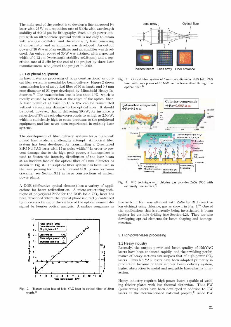
2.3 Peripheral equipmentIn laser materials processing of large constructions, an opti-cal fiber system is essential for beam delivery. Figure 2 showstransmission loss of an optical fiber of 30m length and 0.8mmcore diameter of SI type developed by Mitsubishi Heavy In-dustries.3) The transmission loss is less than 10%, which ismostly caused by reflection at the edges of the optical fiber.A laser power of at least up to 50 kW can be transmittedwithout causing any damage to the optical fiber. It shouldbe noted, however, that in delivering 50 kW, for instance, areflection of 5% at each edge corresponds to as high as 2.5 kW,which is sufficiently high to cause problems to the peripheralequipment and has never been experienced in existing lasersystems.
The development of fiber delivery systems for a high-peakpulsed laser is also a challenging attempt. An optical fibersystem has been developed for transmitting a Q-switchedSHG Nd:YAG laser with 15 ns pulse width.4) In order to pre-vent damage due to the high peak power, a homogenizer isused to flatten the intensity distribution of the laser beamat an incident face of the optical fiber of 1mm diameter asshown in Fig. 3. This optical fiber system has been used inthe laser peening technique to prevent SCC (stress corrosioncracking: see Section 3.1) in large constructions of nuclearpower plants.
A DOE (diffractive optical element) has a variety of appli-cations for beam redistribution. A micro-structuring tech-nique of polycrystal ZnSe for the DOE for a CO2 laser hasbeen developed where the optical phase is directly controlledby microstructuring of the surface of the optical element de-signed by Fourier optical analysis. A surface roughness as
Fig. 2. Transmission loss of Nd: YAG laser in optical fiber of 30mlength.3)
Fig. 3. Optical fiber system of 1mm core diameter SHG Nd: YAGlaser with peak power of 10MW can be transmitted through theoptical fiber.4)
Fig. 4. RIE technique with chlorine gas provides ZnSe DOE withextremely fine surface.5)
fine as 5 nm Ra. was attained with ZnSe by RIE (reactiveion etching) using chlorine, gas as shown in Fig. 4.5) One ofthe applications that is currently being investigated is beamsplitter for via hole drilling (see Section 4.2). They are alsodeveloping optical elements for beam shaping and homoge-nization.
3. High-power-laser processing
3.1 Heavy industryRecently, the output power and beam quality of Nd:YAGlasers have been enhanced rapidly, and their welding perfor-mance of heavy sections can surpass that of high-power CO2
lasers. Thus Nd:YAG lasers have been adopted primarily inproduction because of their simpler beam delivery system,higher absorption to metal and negligible laser-plasma inter-action.
Heavy industry requires high-power lasers capable of weld-ing thicker plates with low thermal distortion. Thus PW(pulse wave) lasers have been developed in addition to CWlasers at the aforementioned national project,1) since PW
21
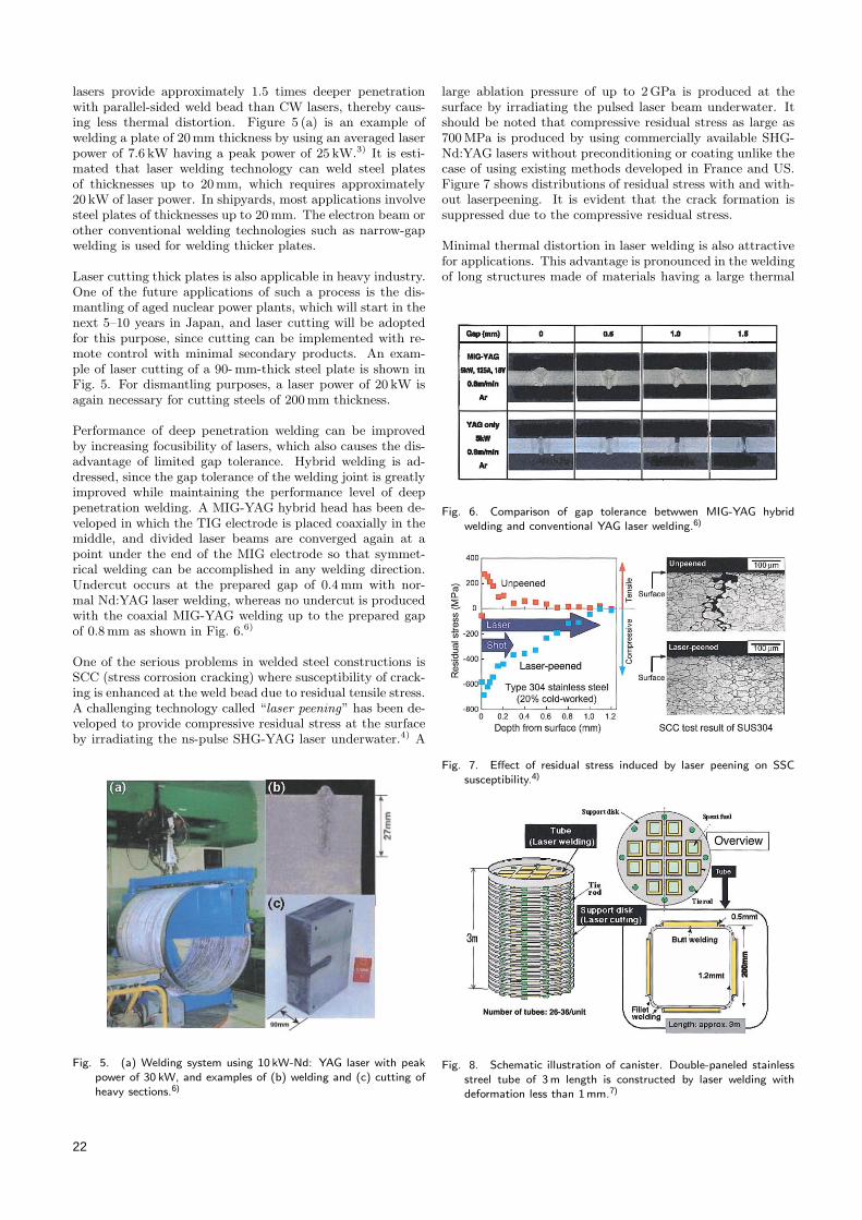
lasers provide approximately 1.5 times deeper penetrationwith parallel-sided weld bead than CW lasers, thereby caus-ing less thermal distortion. Figure 5 (a) is an example ofwelding a plate of 20mm thickness by using an averaged laserpower of 7.6 kW having a peak power of 25 kW.3) It is esti-mated that laser welding technology can weld steel platesof thicknesses up to 20mm, which requires approximately20 kW of laser power. In shipyards, most applications involvesteel plates of thicknesses up to 20mm. The electron beam orother conventional welding technologies such as narrow-gapwelding is used for welding thicker plates.
Laser cutting thick plates is also applicable in heavy industry.One of the future applications of such a process is the dis-mantling of aged nuclear power plants, which will start in thenext 5–10 years in Japan, and laser cutting will be adoptedfor this purpose, since cutting can be implemented with re-mote control with minimal secondary products. An exam-ple of laser cutting of a 90-mm-thick steel plate is shown inFig. 5. For dismantling purposes, a laser power of 20 kW isagain necessary for cutting steels of 200mm thickness.
Performance of deep penetration welding can be improvedby increasing focusibility of lasers, which also causes the dis-advantage of limited gap tolerance. Hybrid welding is ad-dressed, since the gap tolerance of the welding joint is greatlyimproved while maintaining the performance level of deeppenetration welding. A MIG-YAG hybrid head has been de-veloped in which the TIG electrode is placed coaxially in themiddle, and divided laser beams are converged again at apoint under the end of the MIG electrode so that symmet-rical welding can be accomplished in any welding direction.Undercut occurs at the prepared gap of 0.4mm with nor-mal Nd:YAG laser welding, whereas no undercut is producedwith the coaxial MIG-YAG welding up to the prepared gapof 0.8mm as shown in Fig. 6.6)
One of the serious problems in welded steel constructions isSCC (stress corrosion cracking) where susceptibility of crack-ing is enhanced at the weld bead due to residual tensile stress.A challenging technology called “laser peening” has been de-veloped to provide compressive residual stress at the surfaceby irradiating the ns-pulse SHG-YAG laser underwater.4) A
Fig. 5. (a) Welding system using 10 kW-Nd: YAG laser with peakpower of 30 kW, and examples of (b) welding and (c) cutting ofheavy sections.6)
large ablation pressure of up to 2GPa is produced at thesurface by irradiating the pulsed laser beam underwater. Itshould be noted that compressive residual stress as large as700MPa is produced by using commercially available SHG-Nd:YAG lasers without preconditioning or coating unlike thecase of using existing methods developed in France and US.Figure 7 shows distributions of residual stress with and with-out laserpeening. It is evident that the crack formation issuppressed due to the compressive residual stress.
Minimal thermal distortion in laser welding is also attractivefor applications. This advantage is pronounced in the weldingof long structures made of materials having a large thermal
Fig. 6. Comparison of gap tolerance betwwen MIG-YAG hybridwelding and conventional YAG laser welding.6)
Fig. 7. Effect of residual stress induced by laser peening on SSCsusceptibility.4)
Fig. 8. Schematic illustration of canister. Double-paneled stainlessstreel tube of 3m length is constructed by laser welding withdeformation less than 1mm.7)
22
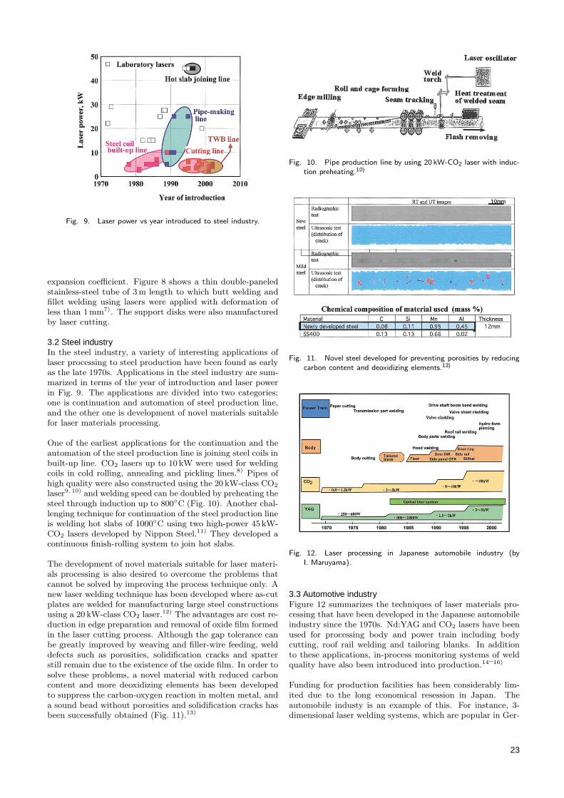
Fig. 9. Laser power vs year introduced to steel industry.
expansion coefficient. Figure 8 shows a thin double-paneledstainless-steel tube of 3m length to which butt welding andfillet welding using lasers were applied with deformation ofless than 1mm7). The support disks were also manufacturedby laser cutting.
3.2 Steel industryIn the steel industry, a variety of interesting applications oflaser processing to steel production have been found as earlyas the late 1970s. Applications in the steel industry are sum-marized in terms of the year of introduction and laser powerin Fig. 9. The applications are divided into two categories;one is continuation and automation of steel production line,and the other one is development of novel materials suitablefor laser materials processing.
One of the earliest applications for the continuation and theautomation of the steel production line is joining steel coils inbuilt-up line. CO2 lasers up to 10 kW were used for weldingcoils in cold rolling, annealing and pickling lines.8) Pipes ofhigh quality were also constructed using the 20 kW-class CO2
laser9, 10) and welding speed can be doubled by preheating thesteel through induction up to 800◦C (Fig. 10). Another chal-lenging technique for continuation of the steel production lineis welding hot slabs of 1000◦C using two high-power 45 kW-CO2 lasers developed by Nippon Steel.
11) They developed acontinuous finish-rolling system to join hot slabs.
The development of novel materials suitable for laser materi-als processing is also desired to overcome the problems thatcannot be solved by improving the process technique only. Anew laser welding technique has been developed where as-cutplates are welded for manufacturing large steel constructionsusing a 20 kW-class CO2 laser.
12) The advantages are cost re-duction in edge preparation and removal of oxide film formedin the laser cutting process. Although the gap tolerance canbe greatly improved by weaving and filler-wire feeding, welddefects such as porosities, solidification cracks and spatterstill remain due to the existence of the oxide film. In order tosolve these problems, a novel material with reduced carboncontent and more deoxidizing elements has been developedto suppress the carbon-oxygen reaction in molten metal, anda sound bead without porosities and solidification cracks hasbeen successfully obtained (Fig. 11).13)
Fig. 10. Pipe production line by using 20 kW-CO2 laser with induc-tion preheating.10)
Fig. 11. Novel steel developed for preventing porosities by reducingcarbon content and deoxidizing elements.13)
Fig. 12. Laser processing in Japanese automobile industry (byI. Maruyama).
3.3 Automotive industryFigure 12 summarizes the techniques of laser materials pro-cessing that have been developed in the Japanese automobileindustry since the 1970s. Nd:YAG and CO2 lasers have beenused for processing body and power train including bodycutting, roof rail welding and tailoring blanks. In additionto these applications, in-process monitoring systems of weldquality have also been introduced into production.14–16)
Funding for production facilities has been considerably lim-ited due to the long economical resession in Japan. Theautomobile industy is an example of this. For instance, 3-dimensional laser welding systems, which are popular in Ger-
23

many, have not been installed until recently in this country.It is interesting, however, that there are more LD-pumpedYAG lasers installed for production in Japan than there arein Germany at the moment. This is probably because thecost of electricity is much higher in Japan than overseas andtherefore, the change of high-power Nd:YAG lasers for mate-rials processing from lump-pumping to LD-pumping occurredquickly even though it started very recently in Japan.
We can find several advanced technologies in the Japaneseautomobile industry. One of the interesting applications islaser cladding of the engine valve and the valve seat in Toy-ota (Fig. 13).16) The conventional press-fit structure of valveseats has been replaced by laser cladding because the walltemperature can be lowered to reduce knocks, and the diam-eter of the valve/seat can become smaller. Toyota introducedlaser-cladding technology into production in 1997 for a typeof sports car, and it is now being used for other popular cars.8 units of 5 kW CO2 lasers yield a production rate of 30000parts per month.
The welding system of plastic intake manifold in whichdiode lasers are used with a 6-axis robot has been developed(Fig. 14).17) The space required for welding facilities that usediode lasers is much smaller than for those that use CO2
and Nd:YAG lasers. This technique is expected to be usedfor a variety of applications in which vibration for joining is
Fig. 13. Laser cladding system for valve seat of 1ZZ-FE engine cylin-der head.16)
Fig. 14. Laser welding system for joining plastic intake manifoldcombined with 6-axis robot.17)
not allowed and the heat-affected zone must be minimized.Joining dissimilar materials including plastic-to-plastic andplastic-to-metal is also a potential application of LD directprocessing.
4. Laser precision microfabrication
4.1 Trend of electronic devicesElectronic devices such as computers, cellular phones, PDAs,and digital cameras are becoming smaller, lighter, and faster.For instance, the weight and the size of cellular phones havedecreased considerably, while their function has markedlyimproved. As a result, the cost of PWB (printed wiringcircuit boards) for cellular phones has rapidly decreased.18)
Miniaturization, high-density packaging and high through-put are demands of manufacturing in the electronic in-dustry. This trend is accompanied by the demands for3-dimensionalization of the electronic devices and opto-electronic integration, and laser materials processing is ex-pected to play an important role in production.
4.2 Via hole drillingOne of the most successful applications of laser materials pro-cessing is via hole drilling of PWB. The world market forbuild-up PWB is increasing steadily due to continuous ex-pansion of the market of electronic consumer products, andJapan’s share in the global micro-via market for PWB is morethan 50% as seen in Fig. 15. The energy source for drillingvia holes of 100–200 µm diameters is CO2 lasers with a pulsewidth of several tens of µs at the moment. The minimumdiameter of the via hole that the CO2 laser can cover hasbecome much smaller than expected due to the improvementof focusing optics and the laser performance, and via holes of30–40 µm diameter have been realized by using the CO2 laser
Fig. 15. World market for build-up PWB (by NEC).
Fig. 16. Micro via holes drilled by CO2 laser (35 µm in diam.) andTHG-Nd: YAG (25µm in diam.).19)
24
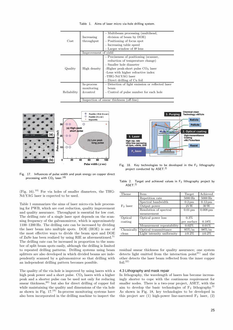
Table 1. Aims of laser micro via-hole drilling system.
- Multibeam processing (multihead,Increasing division of beam by DOE)
Cost throughput - Positioning of focus spot- Increasing table speed- Larger window of fθ lens
Improvement of yield
- Preciseness of positioning (scanner,reduction of temperature change)
- Smaller hole diameterQuality High density -Higher peak-short pulse CO2 laser
-Lens with higher refractive index-THG-Nd:YAG laser- Direct drilling of Cu foil
In-process - Detection of light emission or reflected lasermonitoring beam
Reliability &control - Control of pulse number for each hole
Inspection of smear thickness (off-line)
Fig. 17. Influences of pulse width and peak energy on copper directprocessing with CO2 laser.19)
(Fig. 16).19) For via holes of smaller diameters, the THG-Nd:YAG laser is expected to be used.
Table 1 summarizes the aims of laser micro-via hole process-ing for PWB, which are cost reduction, quality improvementand quality assurance. Throughput is essential for low cost.The drilling rate of a single laser spot depends on the scan-ning frequency of the galvanomirror, which is approximately1100–1200 Hz. The drilling rate can be increased by dividingthe laser beam into multiple spots. DOE (HOE) is one ofthe most effective ways to divide the beam spot and DOEof ZnSe has been realized by using RIE as aforementioned.5)
The drilling rate can be increased in proportion to the num-ber of split beam spots easily, although the drilling is limitedto repeated drilling patterns. Drilling systems using beamsplitters are also developed in which divided beams are inde-pendently scanned by a galvanomirror so that drilling withan independent drilling pattern becomes possible.
The quality of the via hole is improved by using lasers with ahigh peak power and a short pulse. CO2 lasers with a higherpeak and a shorter pulse can be used not only for reducingsmear thickness,20) but also for direct drilling of copper foilwhile maintaining the quality and dimensions of the via holeas shown in Fig. 17.19) In-process monitoring systems havealso been incorporated in the drilling machine to inspect the
Fig. 18. Key technologies to be developed in the F2 lithographyproject conducted by ASET.2)
Table 2. Target and achieved values in F2 lithography project byASET.2)
Theme Item Target Achieved
Repetition rate 5000Hz 5000HzSpectral bandwidth 0.2 pm 0.12 pm
F2 laser Output power 25W 30WResolution of spectral 0.01 pm 0.008 pmmeasurement
Optical Optical power loss 0.3%coating per surface 0.18%
Measurement repeatability 0.02% 0.01%
Chemically Optical transmittance 95%/m 98%/mclean Light intensity uniformity ±0.2% ±0.2%
residual smear thickness for quality assurance; one systemdetects light emitted from the interaction point21) and theother detects the laser beam reflected from the inner copperfoil.22)
4.3 Lithography and mask repairIn lithography, the wavelength of lasers has become increas-ingly shorter to cope with the continuous requirement forsmaller nodes. There is a two-year project, ASET, with theaim to develop the basic technologies of F2 lithography.2)
As shown in Fig. 18, key technologies to be developed inthis project are (1) high-power line-narrowed F2 laser, (2)
25

Fig. 19. Chromium film pattern laser-ablated with pulse width 120 fs (left) and 250 ps(right).25)
Table 3. Road map of mask repair using laser (by NEC).
Year 1981 1985 1991 1995 2000
Node (nm) 2000 1000 700 350 130
Repair accuracy (nm) 500 300 200 100 45
Laser wave-length (nm) 1064 530 351
Pulse width (ns) 20 10 5 0.9 0.25
157 nm optical coating technologies and (3) gas-purging andchemically clean technologies. Table 2 shows the target andachieved values of the project. The high-power F2 laser wasdescribed in 2.2. It is seen that these target values have beensuccessfully achieved in this project.
Technology for repair of photomasks has also been improvedto meet the design rule of photomask patterns. Table 3 showsthe trend of mask repair; wavelength and pulse width of lasersused for mask repair have become shorter. Ns lasers wereused until the 700 nm node, and ps lasers were used afterthe 350 nm node.23) One of the candidates after the 130 nmnode for the near-future design rule is the etching technique.In this technique, laser beam is irradiated in etching atmo-sphere, and a Cr film pattern narrower than the diffractionlimit was realized without any role-up, splash and damage ofthe quartz substrate.24) Another approach is ablation with anultrashort pulse laser to minimize heat dispersion. As seenin Fig. 19, fs lasers of 800 nm wavelength provide better res-olution than ps lasers without vacuum chamber, as well asa linewidth narrower than the diffraction limit due to theirwell-defined threshold of ablation.25)
4.4 Laser microbendingLaser microbending provides new procedures for precise de-formation without mechanical contact, and has a variety ofapplications in production such as for adjustments of mag-netic head height26) and the clearance of lead switch.27) Theseapplications utilize shrinkage stress exerted in the melted por-tion.
A microbending technique without surface damage is real-ized by heating to temperatures just below the melting pointwhere the yield strength is locally lowered. Microbending of aberyllium the melting point where the yield strength is locallylowered. Microbending of a beryllium sheet of 50µm thick-ness has been developed for adjusting micromechanical relays.In this system, Q-switch lasers are used because a steep tem-perature gradient is required for bending thin plates by thismethod.28) Adjusting time is decreased by up to 100ms by an
Fig. 20. Microbending for adjusting matrix-arrayed micro-me-chanical relay by using Q-switch laser.28)
increment control of the beam path from the laser irradiationpoint. This system is soon to be applied to batch productionof matrix-arrayed relays as shown in Fig. 20.
A technique for bending ceramic parts has been developedfor adjusting curvature of the slider in hard disks. Figure 21shows an example of flattening of the slider of an Al2O3-TiCceramic piece of 0.3mm thickness.29) Laser beam spots areirradiated along the automatically detected ridge-line to at-tain a flatness less than 1 nm in the crown, camber and twist.No debris is produced unlike the case of the LCAT (LaserCurvature Adjust Technique) by IBM30) where bending isaccomplished by ablation of a ceramic plate having residualstress.
4.5 Modification of transparent materialAn optical fiber network will soon be available for home use,and optical fiber closures can be observed in the metro area.For optical fiber network, low-cost, reliable, high-performanceoptical devices are required. A fiber bragg grating, which isused for the Add-Drop Module in the WDM (WavelengthDivision Multiplexing) network, can be fabricated by irradi-ation of KrF or ArF excimer laser through the phase mask.Recently, this device has attracted attention because of itslow production cost and long-term reliability (Fig. 22). Theprecise formation of gratings in the very small coupler is veryimportant for high-quality ADMs. Gain flattening of the Er-doped fiber amplifier (EDFA) can be carried out using severallong-period fiber gratings.
A big national project, FESTA (Femto second Technology
26

Fig. 21. Microbending of AI2O3-TiC ceramic for hard disk slider.29)
Fig. 22. Low-cost devices for last mile using grating device writtenby UV laser.
Research Association), is currently under way in Japan. Oneof the goals of this project is to develop a very small waveg-uide using a photonic crystal structure as shown in Fig. 23.31)
Researchers are attempting to fabricate devices using a fslaser for nano-machining technology. This project started in2001 and is now in phase II, which will continue until 2006.
5. Conclusion
Laser materials processing has significantly contributed toJapanese industry in macroprocessing as well as in micropro-cessing. The fact that approximately 25% of all industriallasers worldwide are used for production in Japan indicatesthat Japan is one of the most important countries in termsof laser materials processing. To further increase the applica-tions of laser materials processing for production, innovationof laser technology, peripheral equipment, new materials suit-able for laser materials processing, quality assurance technol-
Fig. 23. Nanofabrication technique of photonic band-gap structuresand ultrasmall optical waveguides using fs laser developed inFESTA.31)
ogy and cost reduction of laser system are required.
The author wishes to thank the members of Japan Laser Pro-cessing Society who provided valuable information for thepresent article.
References1) K. Matsuno: Proc. SPIE 4831 (2002), Paper No. 2302 (in
press).2) H. Komori et al.: Proc. SPIE 4426, 424 (2001); T. Ariga et
al.: Proc. SPIE 4691 (2002), Paper No. 65 (in press).3) T. Ishide et al.: Proc. SPIE 3888, 543 (1999).4) S. Sano et al.: Proc. SPIE 4831 (2002), Paper No. 2306 (in
press); S. Sano: Dissertation, Osaka University (2001), Studyon improvement mechanism of residual stress at metal surfaceby laser irradiation underwater.
5) K. Kurisu et al.: Proc. SPIE 4831 (2002), Paper No. 1279(in press).
6) T. Ishide, M. Nayama, M. Watanabe, and T. Nagashima:International Institute of Welding, IIW-Doc. IV-1708-02
27

(2002); T. Ishide et al: Proc. SPIE 4831 (2002), Paper No.2376 (in press).
7) A. Kitagawa: Dissertation, Osaka University (2001), Funda-mental study on laser applications to large constructions.
8) M. Ito et al.: Proc. 1st Laser Advanced Materials ProcessingCongress (LAMP’87) (1987), p. 535.
9) T. Hayashi, Y. Inaba, T. Kudo, and T. Tanaka: Proc. LaserMaterials Processing Conference, ICALEO’96, LIA Vol. 81(1996), P. D-132.
10) M. Ono, T. Shiozaki, M. Ohmura, H. Nagahama, and K.
Kohno: Proc. ECLAT’96, 6th European Conference on LaserTreatment of Materials (1996), p. 115.
11) K. Minamida: Proc. SPIE 4831 (2002), Paper No. 2363 (inpress).
12) K. Ono, K. Adachi, Y. Matsumoto, I. Miyamoto, and T.Inoue: Proc. Laser Materials Processing Conference, ICA-LEO’99, LIA Vol. 87 (1999), p. D83.
13) K. Ono: Dissertation, Osaka University (2001), Applicationsof high power CO2 laser to manufacturing process of steelstructures.
14) I. Miyamoto, H. Maruo, and Y. Arata: Proc. Laser MaterialsProcessing Conference, ICALEO’84, LIA Vol.44 (1984), p.68.
15) I. Miyamoto, K. Kamimuki, and H. Maruo: Proc. LaserMaterials Processing Conference, ICALEO’93, LIA Vol. 77(1993), p. 413.
16) K. Mikame: Proc. 2nd Laser Advanced Materials ProcessingCongress (LAMP’92) (1992), p. 947.
17) M. Terada and H. Nakamura: Proc. SPIE 4831 (2002), PaperNo. 2346 (in press).
18) I. Miyamoto: Proc. SPIE 4426, 1 (2001).19) A. Fukishima et al.: Electronic packaging technology(in
Japanese), Vol.16, No. 6, June (2000).20) S. Noguchi, E. Ohmura, and I. Miyamoto: Proc. SPIE 4830
(2002), Paper No. 2322 (in press).21) T. Nakayama, T. Sano, I. Miyamoto, K. Tanaka, and Y.
Uchida: Proc. SPIE 3933, 379 (2000).22) K. Ichihashi et al: Proc. Laser Materials Processing Confer-
ence, ICALEO2000 LIA Vol. 90 (2000), p. D36.23) Y. Morishige: Proc. SPIE 4426, 416 (2001).24) Y. Morishige: Private communication.25) T. Okamoto, E. Ohmura, I. Miyamoto, and Y. Morishige:
Proc. SPIE 4830 (2002), Paper No. 1320 (in press).26) K. Funami and T. Okada: J. Jpn. Laser Processing Society(in
Japanese), 4, 253 (1997).27) C. M. Verhoeven, H. F. P. der Bie, and W. Hoving: Proc.
Laser Microfabrication, ICALEO 2000, LIA Vol. 90 (2000),p. B21.
28) K. Kitada and N. Asahi: Proc. SPIE 4830 (2002), Paper No.1204 (in press).
29) N. Matsushita et al: 65th Select Committee Meeting of MicroJoining, Japan Welding Society (in Japanese), Paper No. MJ-390-2001 (2001).
30) A. C. Tam: Proc. SPIE 4088, 380 (2000).31) http://www.festa.or.jp
28