CH7018A TV Encoder / LVDS Transmitter - Chrontel Product... · CH7018A TV Encoder / LVDS...
87
CH7018A 201-0000-043 Rev. 2.2, 1/7/2014 1 Chrontel CH7018A TV Encoder / LVDS Transmitter Features 1.0 General Description TV-Out: • VGA to TV conversion supporting up to 1024x768 pixels. • CH7018A is non- Macrovision™ version). • Two variable-voltage digital input ports. • Simultaneous LVDS and TV output. • True scale rendering engine supporting under-scan in all TV output resolutions. †¥ • Enhanced text sharpness and adaptive flicker removal with up to 7 lines of filtering. ¥ • Support for NTSC and PAL TV formats. • Outputs CVBS, S-Video, RGB and YPrPb. • Support for SCART output. • TV / Monitor connection detect. • Output video switch for easy wiring to connectors. LVDS-Out: • Single / Dual LVDS transmitter. • Dual LVDS supporting pixel rates up to 330Mpixels/sec when both 12-bit input ports are ganged together. • Panel fitting scaler – up scale to 1600x1200 pixels. • LVDS low jitter PLL accepting EMI reduction input. • LVDS 18-bit and 24-bit outputs. • 2D dither engine. • Panel protection and Power-Down sequencing. • Programmable power management. • Support for second CRT DAC bypass mode. • Four 10-bit video DAC outputs. • Fully programmable through serial port. • Complete Windows and DOS driver support. • Variable voltage interface to graphics device. • 128-pin LQFP package. The CH7018A is a Display Controller device that accepts two digital graphics input data streams. One data stream outputs through an LVDS transmitter to a LCD panel, while the other data stream is encoded for NTSC or PAL TV and outputs through four 10-bit high-speed DACs. The TV encoder device encodes a graphics signal up to 1024x768 resolution and outputs the video signals according to NTSC or PAL standards. The LVDS transmitter operates at pixel speeds up to 165MHz per link, supporting 1600x1200 panels at 60Hz refresh rate. The device can also accept one graphics data stream over two 12- bit wide variable voltage ports which support nine different data formats including RGB and YCrCb (RGB must be used for LVDS output). A maximum of 330M pixels per second can be output through dual LVDS links. The TV-Out processor will perform non-interlaced to interlaced conversion with scaling, flicker filtering, and encoding into any of the NTSC or PAL video standards. The scaler and flicker filter are adaptive and programmable for superior text display. Eight graphics resolutions are supported up to 1024 by 768 pixels with full vertical and horizontal under-scan capability in all modes. A high accuracy low jitter phase locked loop is integrated to create outstanding video quality. In addition to TV encoder modes, bypass modes are included which allow the TV DACs to be used as a second CRT DAC. The LVDS transmitter includes a panel fitting up-scaler and a programmable dither function for the support of 18- bit panels. Data is encoded into commonly used formats, including those detailed in the OpenLDI and the SPWG specifications. Serialized data outputs on three to eight differential channels. † Patent number 5,781,241 ¥ Patent number 5,914,753 XCLK1,XCLK1* D1[11:0] H1,V1, DE1 3 12 VREF1 GPIO[5:0] RESET* XI/FIN,XO P-OUT 2 Clock, Data, Sync Latch & Demux LVDS PLL Up-Scaler / Dither LVDS Transmit Clock, Data, Sync Latch & Demux TV PLL Deflicker / Text Enhancement / Scaling / Scan Conversion / TV Encode Four 10-bit DAC's TV Timing LVDS Encode / Serialize Data Mux / Format XCLK2,XCLK2* D2[11:0] H2,V2, DE2 3 12 2 Serial Port Control and Misc. Functions AS SPC SPD LDC[7:4],LDC*[7:4] LL1C,LL1C* LDC[3:0],LDC*[3:0] LL2C, LL2C* DACA[3:0] XTAL 8 2 8 2 2 4 DACB[3:0] 4 FLD/STL1 FLD/STL2 Analog Video Switch 2 BCO/VSYNC C/HSYNC 2 ENAVDD, ENABKL HIN VOUT HOUT HPINT* VIN HPD DD1,DD2 DC1,DC2 SDD,SDC VREF2 Figure 1: CH7018A Functional Block Diagram
Transcript of CH7018A TV Encoder / LVDS Transmitter - Chrontel Product... · CH7018A TV Encoder / LVDS...

CH7018A
201-0000-043 Rev. 2.2, 1/7/2014 1
Chrontel
CH7018A TV Encoder / LVDS Transmitter
Features 1.0 General Description TV-Out: • VGA to TV conversion supporting up to 1024x768
pixels.
• CH7018A is non- Macrovision™ version).
• Two variable-voltage digital input ports.
• Simultaneous LVDS and TV output.
• True scale rendering engine supporting under-scan in all
TV output resolutions. †¥
• Enhanced text sharpness and adaptive flicker removal
with up to 7 lines of filtering. ¥
• Support for NTSC and PAL TV formats.
• Outputs CVBS, S-Video, RGB and YPrPb.
• Support for SCART output.
• TV / Monitor connection detect.
• Output video switch for easy wiring to connectors.
LVDS-Out:
• Single / Dual LVDS transmitter.
• Dual LVDS supporting pixel rates up to 330Mpixels/sec
when both 12-bit input ports are ganged together.
• Panel fitting scaler – up scale to 1600x1200 pixels.
• LVDS low jitter PLL accepting EMI reduction input.
• LVDS 18-bit and 24-bit outputs.
• 2D dither engine.
• Panel protection and Power-Down sequencing.
• Programmable power management.
• Support for second CRT DAC bypass mode.
• Four 10-bit video DAC outputs.
• Fully programmable through serial port.
• Complete Windows and DOS driver support.
• Variable voltage interface to graphics device.
• 128-pin LQFP package.
The CH7018A is a Display Controller device that accepts two
digital graphics input data streams. One data stream outputs
through an LVDS transmitter to a LCD panel, while the other
data stream is encoded for NTSC or PAL TV and outputs through
four 10-bit high-speed DACs. The TV encoder device encodes a
graphics signal up to 1024x768 resolution and outputs the video
signals according to NTSC or PAL standards. The LVDS
transmitter operates at pixel speeds up to 165MHz per link,
supporting 1600x1200 panels at 60Hz refresh rate.
The device can also accept one graphics data stream over two 12-
bit wide variable voltage ports which support nine different data
formats including RGB and YCrCb (RGB must be used for
LVDS output). A maximum of 330M pixels per second can be
output through dual LVDS links.
The TV-Out processor will perform non-interlaced to interlaced
conversion with scaling, flicker filtering, and encoding into any of
the NTSC or PAL video standards. The scaler and flicker filter
are adaptive and programmable for superior text display. Eight
graphics resolutions are supported up to 1024 by 768 pixels with
full vertical and horizontal under-scan capability in all modes. A
high accuracy low jitter phase locked loop is integrated to create
outstanding video quality. In addition to TV encoder modes,
bypass modes are included which allow the TV DACs to be used
as a second CRT DAC.
The LVDS transmitter includes a panel fitting up-scaler and a
programmable dither function for the support of 18-bit panels.
Data is encoded into commonly used formats, including those
detailed in the OpenLDI and the SPWG specifications. Serialized
data outputs on three to eight differential channels.
† Patent number 5,781,241
¥ Patent number 5,914,753
XCLK1,XCLK1*
D1[11:0]
H1,V1, DE13
12
VREF1
GP
IO[5
:0]
RE
SE
T*
XI/FIN,XO
P-OUT2
Clock,
Data,Sync
Latch &Demux
LVDS PLL
Up-Scaler /Dither
LVDS
Transmit
Clock,Data,
Sync
Latch &Demux
TV PLL
Deflicker / Text Enhancement /
Scaling / Scan Conversion /TV Encode
Four10-bit
DAC's
TV Timing
LVDS Encode /Serialize
Da
ta M
ux /
Fo
rma
t
XCLK2,XCLK2*
D2[11:0]
H2,V2, DE23
12
2
Serial Port Control and Misc. Functions
AS
SP
C
SP
D
LDC[7:4],LDC*[7:4]
LL1C,LL1C*LDC[3:0],LDC*[3:0]
LL2C, LL2C*
DACA[3:0]
XTAL
8
2
8
2
2
4
DACB[3:0]4
FLD/STL1
FLD/STL2
Analog
VideoSwitch
2
BCO/VSYNC
C/HSYNC
2ENAVDD, ENABKL
HIN
VO
UT
HO
UT
HP
INT
*
VIN
HP
D
DD
1,D
D2
DC
1,D
C2
SD
D,S
DC
VR
EF
2
Figure 1: CH7018A Functional Block Diagram

CHRONTEL CH7018A
2 201-0000-043 Rev. 2.2 1/7/2014
2.0 Pin Assignment
2.1 Package Diagram
40
41
42
43
44
45
46
47
48
49
50
51
52
53
54
55
56
57
58
59
60
61
62
63
64
39
9089888786858483828180797877767574737271706968676665
969594939291
979899
100101102
DGNDH1V1
DVDDDVDD
XCLK1
XCLK1*
D1[11]D1[10]D1[9]D1[8]D1[7]D1[6]
D1[5]D1[4]D1[3]D1[2]D1[1]D1[0]
DGND
XCLK2
XCLK2*
D2[11]D2[10]D2[9]D2[8]D2[7]D2[6]
D2[5]D2[4]D2[3]D2[2]D2[1]D2[0]
DGND
H2V2
DGND
1234567891011121314151617181920212223242526272829303132333435363738
LL2CLL2C*
LDC7*LDC7
LDC6*LDC6
LDC5*LDC5LVDD
LVDD
LGND
LGND
LGND
LVDDLDC4*LDC4
LL1CLL1C*
LDC2*LDC2
LDC1*LDC1
LDC0*LDC0LVDD
LVDD
LGND
LGND
LGND
LVDD
LDC3*LDC3
ISETDAC_VDD
LPLL_VDD
VSWING
LPLL_GNDLPLLCAP
11
9
10
31
04
10
51
06
11
11
12
11
31
14
11
51
16
11
71
18
10
71
08
10
91
10
12
0
12
7
12
112
212
312
412
512
6
12
8
DV
DD
FL
D/S
TL1
DE
1
Y/G
(D
AC
A1)
CV
BS
(D
AC
A3)
DA
C_G
ND
N/C
Y/G
(D
AC
B1)
C/R
(D
AC
A2)
Pr /
R (
DA
CB
2)
CV
BS
/B (
DA
CA
0)
Pb/B
(D
AC
B0)
TV
PL
L_V
DD
TV
PLL_V
CC
TV
PLL_G
ND
XI / F
IN XO
BC
O/V
SY
NC
VR
EF
1
VD
DV
P- O
UT
DA
C_G
ND
C/H
SY
NC
GP
IO[5
]
GP
IO[4
]
RE
SE
T*
DD
2
AS
GP
IO[3
]G
PIO
[2]
VO
UT
HO
UT
HIN
VIN
HP
D
EN
AB
KL
EN
AV
DD
HP
INT
*
GP
IO[1
]
GP
IO[0
]
SP
DS
PC
DE
2
FLD
/ST
L2
DV
DD
DC
1
VR
EF
2
DD
1
SD
C
DC
2
SD
D
V5V
ChrontelChrontelChrontelChrontelCH7017/CH7018
Figure 2: CH7018A 128 Pin LQFP Package (Top View)

CHRONTEL CH7018A
201-0000-043 Rev. 2.2, 1/7/2014 3
2.2 Pin Description
Table 1: Pin Description
Pin # # of Pins Type Symbol Description
66, 101 2 In/Out H1, H2 Horizontal Sync Input / Output When the SYO control bit is low, these pins accept a horizontal sync inputs
for use with the input data. The amplitude will range from 0 to VDDV.
VREF1 is the threshold level for these inputs. These pins must be used as
inputs in RGB Bypass mode.
When the SYO control bit is high, the TV encoder will output a 64-pixels
wide horizontal sync pulse from one of these pins. The output is driven
from the DVDD supply, and it is valid ONLY when TV-Out is in operation.
65, 102 2 In/Out V1, V2 Vertical Sync Input / Output When the SYO control bit is low, these pins accept a vertical sync inputs for
use with the input data. The amplitude will range from 0 to VDDV.
VREF1 is the threshold level for these inputs. These pins must be used as
inputs in RGB Bypass mode.
When the SYO control bit is high, the TV encoder will output a 1-line wide
vertical sync pulse from one of these pins. The output is driven from the
DVDD supply, and it is valid ONLY when TV-Out is in operation.
63, 104 2 In
DE1, DE2 Data Enable These pins accept a data enable signal that is high when active video data is
input to the device, and remains low during all other times. The amplitude
will range from 0 to VDDV. VREF1 is the threshold level for these inputs.
The TV-Out function uses H and V sync signals and values in the SAV
Register as reference to active video.
62, 105 2 Out FLD/STL1,
FLD/STL2 TV Field / Flat Panel Stall Signal These outputs can be programmed to be either a TV Field output from the
TV encoder, or a Stall output from the flat panel Up-scaler. These outputs
are tri-stated upon power up.
107 1 In/Out SPD Serial Port Data Input / Output This pin functions as the bi-directional data pin of the serial port. It can
operate with input levels from VDDV to DVDD. Outputs are driven from 0
to VREF2.
108 1 In SPC Serial Port Clock Input This pin functions as the clock input of the serial port. It can operate with
input levels from VDDV to DVDD.
106 1 In AS Address Select (Internal Pull-up)
This pin determines the device address of the serial port.
112 1 In/Out SDD Low-Voltage DDC Serial Data Low-voltage serial data for DDC. It uses VREF2 / 2 as the threshold
voltage. VREF2 divide by 2 function is generated on-chip.
113 1 In/Out SDC Low-Voltage DDC Serial Clock
Low-voltage serial clock for DDC. It uses VREF2 / 2 as the threshold
voltage. VREF2 divide by 2 function is generated on-chip.
114, 116 2 In/Out DD1, DD2 DDC Serial Data Serial data for DDC. (0V to 5V)
111 1 In VREF2 Reference Voltage 2 Used to generate the output supply level for the SPD port. This pin should
be tied externally to the maximum voltage seen by the ports. (1.5V to 3.3V).
115, 117 2 In/Out DC1, DC2 DDC Serial Clock
Clock for DDC. (0V to 5V)
123-126, 56,
57
6 In/Out GPIO[5:0] General Purpose Input / Output [5:0] These pins provide general purpose I/O and are controlled via the serial port.
(3.3V). See description of GPIO Controls for I/O configuration.
127 1 Out ENAVDD Panel Power Enable Enable panel VDD. (3.3V)
128 1 Out ENABLK Back Light Enable
Enable Back-Light of LCD Panel. (3.3V)

CHRONTEL CH7018A
4 201-0000-043 Rev. 2.2 1/7/2014
Table 1: Pin Description (Continued)
Pin # # of Pins Type Symbol Description
121 1 In
HPD
Hot Plug Detect (Internal Pull-down)
This input pin determines whether a display device is connected to the
VGA connector. When terminated, the display device is required to
apply a voltage greater than 2.4 volts. Changes on the status of this pin
will be relayed to the graphics controller via the HPINT* pin pulling low.
122 1 Out
HPINT*
Hot Plug Interrupt Output This pin provides an open drain output, which pulls low when a
termination change has been detected on the HPD input.
36 1 In VSWING LVDS Voltage Swing Control
This pin sets the swing level of the LVDS outputs. A 2.4K Ohm resistor
should be connected between this pin and LGND (pin 35) using short and
wide traces.
58 1 In RESET* Reset * Input (Internal Pull-up)
When this pin is low, the device is held in the power-on reset condition.
When this pin is high, reset is controlled through the serial port.
2 1 Analog LPLLCAP LVDS PLL Capacitor This pin allows coupling of any signal to the on-chip loop filter capacitor.
5, 24 2 Out LL2C, LL1C Positive LVDS differential Clock2 & Clock1
6, 25 2 Out LL2C*, LL1C* Negative LVDS differential Clock2 & Clock1
8, 11, 14, 17 4 Out LDC[7:4] Positive LVDS differential data[7:4]
9, 12, 15, 18 4 Out LDC[7:4]* Negative LVDS differential data[7:4]
21, 27, 30, 33 4 Out LDC[3:0] Positive LVDS differential data[3:0]
22, 28, 31, 34 4 Out LDC[3:0]* Negative LVDS differential data [3:0]
38 1 Analog ISET Current Set Resistor Input This pin sets the DAC current. A 140-ohm resistor should be connected
between this pin and DAC_GND (pin 39) using short and wide traces.
41 1 Out CVBS (DACA3)
Composite Video This pin outputs a composite video signal capable of driving a 75 ohm doubly terminated load. During bypass modes this output is valid only if the data format is compatible with one of the TV-Out display modes.
42 1 Out Y/G (DACB1)
Luma / Green Output This pin outputs a selectable video signal. The output is designed to drive a 75
ohm doubly terminated load. The output can be selected to be the luminance
component of YPrPb or green (for VGA bypass)
43 1 Out Y/G (DACA1)
Luma / Green Output This pin outputs a selectable video signal. The output is designed to drive a 75
ohm doubly terminated load. The output can be selected to be s-video luminance
or green (for SCART type 1 connections) or the luminance component of YPrPb or
green (for VGA bypass)
44 1 Out Pr/R (DACB2)
Pr / Red Output This pin outputs a selectable video signal. The output is designed to drive a 75
ohm doubly terminated load. The output can be selected to be the Pr component of
YPrPb or red (for VGA bypass)
45 1 Out C/R/Pr (DACA2)
Chroma / Red Output This pin outputs a selectable video signal. The output is designed to drive a 75
ohm doubly terminated load. The output can be selected to be s-video
chrominance or red (for SCART type 1 connections) or the Pr component of
YPrPb or red (for VGA bypass)
46 1 Out Pb/B (DACB0)
Pb / Blue Output This pin outputs a selectable video signal. The output is designed to drive a 75
ohm doubly terminated load. The output can be selected to the Pb component of
YPrPb or blue (for VGA bypass).
47 1 Out CVBS/B/Pb (DACA0)
Composite Video / Blue Output This pin outputs a selectable video signal. The output is designed to drive a 75
ohm doubly terminated load. The output can be selected to be composite video or
blue (for SCART type 1 connections) or the Pb component of YPrPb or blue (for
VGA bypass).
120 1 Out VOUT V-Sync Output This pin is the output of a voltage translating digital buffer and is driven
from V5V.

CHRONTEL CH7018A
201-0000-043 Rev. 2.2, 1/7/2014 5
Table 1: Pin Description (Continued)
Pin # # of Pins Type Symbol Description
110 1 In VIN V-Sync Input This pin is the input of a voltage translating digital buffer. Input threshold
can be programmed by serial port to equal to VREF2/2 or to DVDD/2.
119 1 Out HOUT H-Sync Output This pin is the output of a voltage translating digital buffer and is driven
from V5V.
109 1 In HIN H-Sync Input This pin is the input of a voltage translating digital buffer. Input threshold
can be programmed by serial port to equal to VREF2/2 or to DVDD/2
49 1 Out C/HSYNC Composite / Horizontal Sync This pin provides composite sync in TV modes and horizontal sync in
bypass RGB mode. This pin is driven by the DVDD supply.
50 1 Out BCO/VSYNC Buffered Clock Outputs / Vertical Sync This output pin provides buffered crystal oscillator clock output or
VSYNC output in bypass RGB mode. This pin is driven by the DVDD
supply.
52 1 In XI / FIN Crystal Input / External Reference Input A parallel resonant 14.31818MHz crystal (+ 20 ppm) should be attached
between this pin and XO. However, an external CMOS compatible clock
can drive the XI/FIN input.
53 1 Out XO Crystal Output A parallel resonance 14.31818MHz crystal (+ 20 ppm) should be attached
between this pin and XI / FIN. However, if an external CMOS clock is
attached to XI/FIN, XO should be left open.
59 1 Out P-Out Pixel Clock Output
This pin provides a pixel clock signal to the VGA controller, which can
be used as a reference frequency. The output is selectable between 1X
and 2X of the pixel clock frequency. The output driver is driven from
the VDDV supply (pin 60). This output has a programmable tri-state.
The capacitive loading on this pin should be kept to a minimum.
61 1 In VREF1 Reference Voltage Input 1 The VREF1 pin inputs a reference voltage of VDDV / 2. The signal is
derived externally through a resistor divider and decoupling capacitor,
and will be used as a reference level for data, sync and clock inputs.
68-73, 77-82
12 In D1[11:0]
Data1[11] through Data1[0] Inputs These pins accept the 12 data inputs from a digital video port of a
graphics controller. The levels are 0 to VDDV. VREF1 is the threshold
level.
76, 74 2 In XCLK1,
XCLK1* External Clock Inputs These inputs form a differential clock signal input to the device for use
with the H1, V1 and D1[11:0] data. If differential clocks are not
available, the XCLK1* input should be connected to VREF1. The clock
polarity can be selected by the MCP1 control bit.
85-90, 94-99 12 In D2[11:0] Data2[11] through Data2[0] Inputs These pins accept the 12 data inputs from a digital video port of a
graphics controller. The levels are 0 to VDDV. VREF1 is the threshold
level.
93, 91 2 In XCLK2,
XCLK2* External Clock Inputs These inputs form a differential clock signal input to the device for use
with the H2, V2 and D2[11:0] data. If differential clocks are not
available, the XCLK2* input should be connected to VREF1. The clock
polarity can be selected by the MCP2 control bit.
118 1 Power V5V 5V supply for H/VOUT (5V)
64, 83, 84, 103 4 Power DVDD Digital Supply Voltage (3.3V)
67, 75, 92, 100 4 Power DGND Digital Ground
60 1 Power VDDV I/O Supply Voltage (1.1V to 3.3V)
55 2 Power TVPLL_VDD TV PLL Supply Voltage (3.3V)
54 1 Power TVPLL_VCC TV PLL Supply Voltage (3.3V)
51 1 Power TVPLL_GND TV PLL Ground
37 1 Power DAC_VDD DAC Supply Voltage (3.3V)

CHRONTEL CH7018A
6 201-0000-043 Rev. 2.2 1/7/2014
Table 1: Pin Description (Continued)
Pin # # of Pins Type Symbol Description
39, 48 1 Power DAC_GND DAC Ground
7, 13, 19, 20,
26, 32
6 Power LVDD LVDS Supply Voltage (3.3V)
4, 10, 16, 23,
29, 35
6 Power LGND LVDS Ground
1 1 Power LPLL_VDD LVDS PLL Supply Voltage (3.3V)
3 1 Power LPLL_GND LVDS PLL Ground

CHRONTEL CH7018A
201-0000-043 Rev. 2.2, 1/7/2014 7
3.0 Overview
The CH7018A is a VGA to TV encoder with dual LVDS output for the graphics subsystem. Both TV-Out and LVDS-
Out can operate simultaneously if the two 12-bit input ports are driven from different timing generators. TV timing
requirements are usually different from that of the TFT-LCD panels. If the graphics controller can generate only one set
of timing, simultaneous display on both the TV and the flat panel may not be available for all graphics modes. The
blockdiagram of the device and the data flow within it is shown on Figure 1.
The CH7018A also supports 24-bit input mode by ganging D1 and D2 together as a single 24-bit data port. In this case
the timing signals H1, V1, DE1, XCLK1 and XCLK1* are equal to H2, V2, DE2, XCLK2 and XCL2*, respectively.
Video data are sent to either the TV encoder (including RGB bypass) or to the LVDS data path, but not both. Maximum
data rate supported through the dual LVDS links is 330M Pixels /sec. The maximum pixel rate supported by the RGB
bypass mode is 165 Mpixels/sec.
3.1 Input Interface Timing
Four distinct methods of transferring data to the CH7018A are described below. In each of the four modes, DEx is used
to signal active LVDS data for the panel and register SAV value denotes the start of active TV video.
A. 12-bit Multiplexed Data – Dual-edge Transfer
• Multiplexed data - two 12-bit words per pixel from either D1[11:0] or D2[11:0]
• Clock frequency equals 1X pixel rate with 12-bit data transfer at both rising and falling clock edges.
• Maximum pixel rate is 165M pixels per second with a 165 MHz pixel clock.
Simultaneous TV and panel display.
D x [ 1 1 : 0 ]
H x
V x
D E x
6 4 P - O U T
t S t H
t Ht S
> = 1 V G A L in e
X C L K x
X C L K x *S A V
Figure 3: Interface Timing for Multiplexed Data – Dual-edge Transfer
B. 12-bit Multiplexed Data – Single-edge Transfer
• Multiplexed data - two 12-bit words per pixel from either D1[11:0] or D2[11:0]
• Clock frequency equals 2X pixel rate with 12-bit data transfer at either rising or falling edge of clock
(programmable via serial port).
• Maximum pixel rate is 165M pixels per second with a 330 MHz pixel clock.
• Simultaneous TV and panel display.

CHRONTEL CH7018A
8 201-0000-043 Rev. 2.2 1/7/2014
Figure 4: Interface Timing for Multiplexed Data – Single-edge Transfer
C. 24-bit Ganged Data – Dual-edge Transfer
• Multiplexed data - two 24-bit words per pixel from both D1[11:0] and D2[11:0]
• Clock frequency equals 1/2X pixel rate with 24-bit data transfer at both rising and falling clock edges.
• Maximum pixel rate is 330M pixels per second with a 165 MHz pixel clock.
• No Simultaneous TV and LVDS panel display.
Figure 5: Interface Timing for 24-bit Multiplexed Data – Dual-edge Transfer
D. 24-bit Ganged Data – Single-edge Transfer
• Non-multiplexed data - one 24-bit word per pixel from both D1[11:0] and D2[11:0].
• Clock frequency equals 1X pixel rate with 24-bit data transfer at either rising or falling edge of clock
(programmable via serial port).
• Maximum pixel rate is 330M pixels per second with a 330 MHz pixel clock.
• No simultaneous TV and LVDS panel display.
D x [ 1 1 : 0 ]
X C L K x
X C L K x *
H x
V x
D E x
6 4 P - O U T
t S
S
t H
t Ht S
> = 1 V G A L in e
S A V
D 1 [ 1 1 : 0 ]
D 2 [ 1 1 : 0 ]
H x
V x
D E x
6 4 P - O U T
t S t H
t Ht S
> = 1 V G A L in e
X C L K x
X C L K x *S A V

CHRONTEL CH7018A
201-0000-043 Rev. 2.2, 1/7/2014 9
D 1 [ 1 1 : 0 ]
D 2 [ 1 1 : 0 ]
X C L K x
X C L K x *
H x
V x
D E x
6 4 P - O U T
t S t H
t Ht S
> = 1 V G A L i n e
S A V
Figure 6: Interface Timing for Non-multiplexed Data – Single-edge Transfer
Table 2: Interface Timing Specifications
Symbol Parameter Min Typ Max Unit
tS Setup time See section 5.5 ns
tH Hold time See section 5.5 ns
Note: tS, tH, setup time and hold time are programmable through serial port – X1CMD [3:0] and X2CMD[3:0] by delay
or advance of clock relative to data.

CHRONTEL CH7018A
10 201-0000-043 Rev. 2.2 1/7/2014
3.2 Input Data Formats
3.2.1 12-Bit Multiplexed Data Formats
Multiplexed pixel data inputs to the CH7018A through D1[11:0] or D2[11:0] using data transfer method A or B is
described in 3.1. Received data is formatted and sent through an internal data bus P1[23:0] to TV encoder or directly to
the TV DACs, or through bus P2[23:0] to the LVDS data path. The multiplexed input data formats are
(IDF1[3:0]=0,1,2,3 and 4 for D1 and IDF2[3:0]=0,1,2,3 and 4 for D2):
IDFx Description 0 RGB 8-8-8 (2x12-bit)
1 RGB 8-8-8 (2x12-bit) or RGB 5-6-5 (2x8-bit)
2 RGB 5-6-5 (2x8bit)
3 RGB 5-5-5 (2x8-bit)
4 YCrCb 8-8 (2x8-bit)
For multiplexed input data formats, data can be latched from the graphics controller by either rising only or falling only
clock edges, or by both rising and falling clock edges. The MCPx bits select the rising or the falling clock edge, where
rising refers to rising edge on the XCLKx signals and falling edge on the XCLKx* signals. The multiplexed input data
formats are shown in Figure 7. The input data bus Dx[11:0], where x can be either 1 or 2, transports a 12-bit or 8-bit
multiplexed data stream containing either RGB or YCrCb formatted data. The input data rate is 2X the pixel rate and
each pair of Pn values (e.g.; P0a and P0b) contains a complete pixel encoded as shown in the Tables 3 to 6 below and
can be placed onto one or both of the internal pixel buses Py[23:0], where y equals 1 or 2. It is assumed that the first
clock cycle following the leading edge of the incoming horizontal sync signal contains the first word (Pxa) of a pixel, if
an active pixel was present immediately following the horizontal sync. When the input is a YCrCb data stream the
color-difference data will be transmitted at half the data rate of the luminance data with the sequence being set as Cb0,
Y0, Cr0, Y1, where Cb0,Y0,Cr0 refers to co-sited luminance and color-difference samples and the following Y1 byte
refers to the next luminance sample, per CCIR-656 standards (the clock frequency is dependent upon the current mode,
and is not 27MHz as specified in CCIR-656). All non-active pixels should be 0 in RGB formats, and 16 for Y and 128
for CrCb in YCrCb formats.
Dx[11:0]
Hx
XCLKx(2X)
P1aP0a P2aP1bP0b P2b
SAV
XCLKx(1X)
DEx
Figure 7: 12-bit Multiplexed Input Data Formats (IDFx = 0,1,2,3,4)

CHRONTEL CH7018A
201-0000-043 Rev. 2.2, 1/7/2014 11
Table 3: Multiplexed Input Data Formats (IDFx = 0, 1)
IDFx =
Format =
0
RGB 8-8-8 (2x12-bit)
For TV/Bypass RGB or/and LVDS
1
RGB 8-8-8 (2x12-bit)
or RGB 5-6-5 (2x8-bit)
For TV/Bypass RGB or/and LVDS
Pixel # P0a P0b P1a P1b P0a P0b P1a P1b
Bus Data Dx[11] G0[3] R0[7] G1[3] R1[7] G0[4] R0[7] G1[4] R1[7]
Dx[10] G0[2] R0[6] G1[2] R1[6] G0[3] R0[6] G1[3] R1[6]
Dx[9] G0[1] R0[5] G1[1] R1[5] G0[2] R0[5] G1[2] R1[5]
Dx[8] G0[0] R0[4] G1[0] R1[4] B0[7] R0[4] B1[7] R1[4]
Dx[7] B0[7] R0[3] B1[7] R1[3] B0[6] R0[3] B1[6] R1[3]
Dx[6] B0[6] R0[2] B1[6] R1[2] B0[5] G0[7] B1[5] G1[7]
Dx[5] B0[5] R0[1] B1[5] R1[1] B0[4] G0[6] B1[4] G1[6]
Dx[4] B0[4] R0[0] B1[4] R1[0] B0[3] G0[5] B1[3] G1[5]
Dx[3] B0[3] G0[7] B1[3] G1[7] G0[0] R0[2] G1[0] R1[2]
Dx[2] B0[2] G0[6] B1[2] G1[6] B0[2] R0[1] B1[2] R1[1]
Dx[1] B0[1] G0[5] B1[1] G1[5] B0[1] R0[0] B1[1] R1[0]
Dx[0] B0[0] G0[4] B1[0] G1[4] B0[0] G0[1] B1[0] G1[1]
Table 4: Multiplexed Input Data Formats (IDFx = 2, 3)
IDFx =
Format =
2
RGB 5-6-5 (2x8bit)
For TV/Bypass RGB or/and LVDS
3
RGB 5-5-5 (2x8-bit)
for TV/Bypass RGB or/and LVDS
Pixel # P0a P0b P1a P1b P0a P0b P1a P1b
Bus Data Dx[11] G0[4] R0[7] G1[4] R1[7] G0[5] X G1[5] X
Dx[10] G0[3] R0[6] G1[3] R1[6] G0[4] R0[7] G1[4] R1[7]
Dx[9] G0[2] R0[5] G1[2] R1[5] G0[3] R0[6] G1[3] R1[6]
Dx[8] B0[7] R0[4] B1[7] R1[4] B0[7] R0[5] B1[7] R1[5]
Dx[7] B0[6] R0[3] B1[6] R1[3] B0[6] R0[4] B1[6] R1[4]
Dx[6] B0[5] G0[7] B1[5] G1[7] B0[5] R0[3] B1[5] R1[3]
Dx[5] B0[4] G0[6] B1[4] G1[6] B0[4] G0[7] B1[4] G1[7]
Dx[4] B0[3] G0[5] B1[3] G1[5] B0[3] G0[6] B1[3] G1[6]
Table 5: Multiplexed Input Data Formats (IDFx = 4)
IDFx =
Format =
4
YCrCb 4:2:2 (2x8-bit)
for TV
Pixel # P0a P0b P1a P1b P2a P2b P3a P3b
Bus Data Dx[7] Cb0[7] Y0[7] Cr0[7] Y1[7] Cb2[7] Y2[7] Cr2[7] Y3[7]
Dx[6] Cb0[6] Y0[6] Cr0[6] Y1[6] Cb2[6] Y2[6] Cr2[6] Y3[6]
Dx[5] Cb0[5] Y0[5] Cr0[5] Y1[5] Cb2[5] Y2[5] Cr2[5] Y3[5]
Dx[4] Cb0[4] Y0[4] Cr0[4] Y1[4] Cb2[4] Y2[4] Cr2[4] Y3[4]
Dx[3] Cb0[3] Y0[3] Cr0[3] Y1[3] Cb2[3] Y2[3] Cr2[3] Y3[3]
Dx[2] Cb0[2] Y0[2] Cr0[2] Y1[2] Cb2[2] Y2[2] Cr2[2] Y3[2]
Dx[1] Cb0[1] Y0[1] Cr0[1] Y1[1] Cb2[1] Y2[1] Cr2[1] Y3[1]
Dx[0] Cb0[0] Y0[0] Cr0[0] Y1[0] Cb2[0] Y2[0] Cr2[0] Y3[0]
When IDFx = 4 (YCrCb mode), the data inputs can also be used to transmit sync information to the device. In this
mode, the embedded sync will follow the VIP2 convention, and the first byte of the ‘video timing reference code’ will be
assumed to occur when a Cb sample would occur, if the video stream is continuous.

CHRONTEL CH7018A
12 201-0000-043 Rev. 2.2 1/7/2014
Table 6: Multiplexed Input Data Formats (IDFx = 4) with Embedded Sync
IDFx =
Format =
4
YCrCb 4:2:2 (2x8-bit) for TV
Pixel # P0a P0b P1a P1b P2a P2b P3a P3b
Bus Data Dx[7] 1 0 0 S[7] Cb2[7] Y2[7] Cr2[7] Y3[7]
Dx[6] 1 0 0 S[6] Cb2[6] Y2[6] Cr2[6] Y3[6]
Dx[5] 1 0 0 S[5] Cb2[5] Y2[5] Cr2[5] Y3[5]
Dx[4] 1 0 0 S[4] Cb2[4] Y2[4] Cr2[4] Y3[4]
Dx[3] 1 0 0 S[3] Cb2[3] Y2[3] Cr2[3] Y3[3]
Dx[2] 1 0 0 S[2] Cb2[2] Y2[2] Cr2[2] Y3[2]
Dx[1] 1 0 0 S[1] Cb2[1] Y2[1] Cr2[1] Y3[1]
Dx[0] 1 0 0 S[0] Cb2[0] Y2[0] Cr2[0] Y3[0]
In this mode, the S[7..0] byte contains the following data:
S[6] = F = 1 during field 2, 0 during field 1
S[5] = V = 1 during field blanking, 0 elsewhere
S[4] = H = 1 during EAV (synchronization reference at the end of active video)
0 during SAV (synchronization reference at the start of active video)
S[7] and S[3:0] are ignored.
3.2.2 24-Bit Data Formats
The two 12-bit input data ports, D1[11:0] and D2[11:0], can be grouped together to form a single 24-bit interface to the
graphic controller. In this case the timing signals H1, V1, DE1, XCLK1 and XCLK1* are equal to H2, V2, DE2,
XCLK2 and XCL2* , respectively. The CH7018A supports 5 different 24-bit data formats. Each of which is used with a
1X pixel rate clock latching data with one of the clock edges (default is falling edge). The 24-bit input data formats are
IDFx[3:0]=5,6,7,8 and 9 (note that IDF1 must be set equal to IDF2) and are illustrated in Figure 8 below.
IDFx Description
5 RGB 8-8-8 (1x24-bit) for TV/Bypass RGB
6 YCrCb 8-8 (1x16-bit with CrCb multiplexed and decimated by 2) for TV
7 YCrCb 8-8-8 (1x24-bit) for TV
8 RGB 8-8-8 (2x24-bit) Odd / Even Ganged for LVDS
9 RGB 8-8-8 (1x24-bit) Normal Ganged for LVDS
The pixel data bus represents a 24-bit or 16-bit data stream containing either RGB or YCrCb formatted data. When the
input is a 16-bit YCrCb data stream the color-difference data will be transmitted at half the data rate of the luminance
data, with the sequence being set as Cb0, Y0 transmitted during one clock cycle, followed by Cr0, Y1 the following
clock cycle, where Cb0,Y0,Cr0 refers to co-sited luminance and color-difference samples and the Y1 data refers to the
next luminance sample, per CCIR-601 sampling. Non-active data must be 0 in RGB format, and 16 for Y, 128 for Cr
and Cb in YCrCb formats.
P0 P1 P2 P3 P4 P5
SAV
XCLKx
DEx
Dx[11:0]
Hx
Figure 8: Non-Multiplexed Input Data Formats (IDFx = 5,6,7,8 and 9)

CHRONTEL CH7018A
201-0000-043 Rev. 2.2, 1/7/2014 13
Table 7: Non-Multiplexed Data Formats
IDFx =
Format =
5
24-bit RGB for
TV/Bypass RGB
6 16-bit YCrCb
FOR TV
7
24-bit YCrCb
FOR TV
Pixel # P0 P1 P0 P1 P2 P3 P0 P1
Bus Data D1[11] R0[7] R1[7] Y0[7] Y1[7] Y2[7] Y3[7] Y0[7] Y1[7]
D1[10] R0[6] R1[6] Y0[6] Y1[6] Y2[6] Y3[6] Y0[6] Y1[6]
D1[9] R0[5] R1[5] Y0[5] Y1[5] Y2[5] Y3[5] Y0[5] Y1[5]
D1[8] R0[4] R1[4] Y0[4] Y1[4] Y2[4] Y3[4] Y0[4] Y1[4]
D1[7] R0[3] R1[3] Y0[3] Y1[3] Y2[3] Y3[3] Y0[3] Y1[3]
DVOB D1[6] R0[2] R1[2] Y0[2] Y1[2] Y2[2] Y3[2] Y0[2] Y1[2]
D1[5] R0[1] R1[1] Y0[1] Y1[1] Y2[1] Y3[1] Y0[1] Y1[1]
D1[4] R0[0] R1[0] Y0[0] Y1[0] Y2[0] Y3[0] Y0[0] Y1[0]
D1[3] G0[7] G1[7] Cr0[7] Cb0[7] Cr2[7] Cb2[7] Cr0[7] Cr1[7]
D1[2] G0[6] G1[6] Cr0[6] Cb0[6] Cr2[6] Cb2[6] Cr0[6] Cr1[6]
D1[1] G0[5] G1[5] Cr0 [5] Cb0 [5] Cr2 [5] Cb2 [5] Cr0 [5] Cr1 [5]
D1[0] G0[4] G1[4] Cr0 [4] Cb0 [4] Cr2 [4] Cb2 [4] Cr0 [4] Cr1 [4]
D2[11] G0[3] G1[3] Cr0 [3] Cb0 [3] Cr2 [3] Cb2 [3] Cr0 [3] Cr1 [3]
D2[10] G0[2] G1[2] Cr0 [2] Cb0 [2] Cr2 [2] Cb2 [2] Cr0 [2] Cr1 [2]
D2[9] G0[1] G1[1] Cr0 [1] Cb0 [1] Cr2 [1] Cb2 [1] Cr0 [1] Cr1 [1]
D2[8] G0[0] G1[0] Cr0 [0] Cb0 [0] Cr2 [0] Cb2 [0] Cr0 [0] Cr1 [0]
D2[7] B0[7] B1[7] Cb0[7] Cb1[7]
DVOC D2[6] B0[6] B1[6] Cb0[6] Cb1[6]
D2[5] B0[5] B1[5] Cb0 [5] Cb1[5]
D2[4] B0[4] B1[4] Cb0 [4] Cb1[4]
D2[3] B0[3] B1[3] Cb0 [3] Cb1[3]
D2[2] B0[2] B1[2] Cb0 [2] Cb1[2]
D2[1] B0[1] B1[1] Cb0 [1] Cb1[1]
D2[0] B0[0] B1[0] Cb0 [0] Cb1[0]
CHRONTEL CH7018A
14 201-0000-043 Rev. 2.2 1/7/2014
When IDFx = 6 or 7 (YCrCb modes), the data inputs can be used to transmit sync information to the device. In these
modes the embedded sync follows a subset of the VIP2 convention, and the first byte of the video timing reference code
is assumed to occur when a Cb sample occurs, if the video stream is continuous. This is shown in Table 8 below.
Table 8: Non-Multiplexed YCrCb modes with Embedded Sync
IDFx =
Format =
6
16-bit YCrCb
for TV
7
24-bit YCrCb
for TV
Pixel # P0 P1 P2 P3 P0 P1 P2 P3
Bus Data D1[11] 0 S[7] Y0[7] Y1[7] 0 S[7] Y0[7] Y1[7]
D1[10] 0 S[6] Y0[6] Y1[6] 0 S[6] Y0[6] Y1[6]
D1[9] 0 S[5] Y0[5] Y1[5] 0 S[5] Y0[5] Y1[5]
D1[8] 0 S[4] Y0[4] Y1[4] 0 S[4] Y0[4] Y1[4]
D1[7] 0 S[3] Y0[3] Y1[3] 0 S[3] Y0[3] Y1[3]
D1[6] 0 S[2] Y0[2] Y1[2] 0 S[2] Y0[2] Y1[2]
D1[5] 0 S[1] Y0[1] Y1[1] 0 S[1] Y0[1] Y1[1]
D1[4] 0 S[0] Y0[0] Y1[0] 0 S[0] Y0[0] Y1[0]
D1[3] 1 0 Cr0[7] Cb0[7] 1 X Cr0[7] Cr1[7]
D1[2] 1 0 Cr0[6] Cb0[6] 1 X Cr0[6] Cr1[6]
D1[1] 1 0 Cr0 [5] Cb0 [5] 1 X Cr0 [5] Cr1[5]
D1[0] 1 0 Cr0 [4] Cb0 [4] 1 X Cr0 [4] Cr1[4]
D2[11] 1 0 Cr0 [3] Cb0 [3] 1 X Cr0 [3] Cr1[3]
D2[10] 1 0 Cr0 [2] Cb0 [2] 1 X Cr0 [2] Cr1[2]
D2[9] 1 0 Cr0 [1] Cb0 [1] 1 X Cr0 [1] Cr1[1]
D2[8] 1 0 Cr0 [0] Cb0 [0] 1 X Cr0 [0] Cr1[0]
D2[7] 0 X Cb0[7] Cb1[7]
D2[6] 0 X Cb0[6] Cb1[6]
D2[5] 0 X Cb0 [5] Cb1 [5]
D2[4] 0 X Cb0 [4] Cb1 [4]
D2[3] 0 X Cb0 [3] Cb1 [3]
D2[2] 0 X Cb0 [2] Cb1 [2]
D2[1] 0 X Cb0 [1] Cb1 [1]
D2[0] 0 X Cb0 [0] Cb1 [0]
In this mode, the S[7:0] byte contains the following data:
S[6] = F = 1 during field 2, 0 during field 1
S[5] = V = 1 during field blanking, 0 elsewhere
S[4] = H = 1 during EAV (synchronization reference at the end of active video)
0 during SAV (synchronization reference at the start of active video)
S[7] and S[3:0] are ignored
Under modes 8 and 9, the CH7018A takes 24-bit data from both D1 and D2 and outputs to the dual LVDS links. A
maximum throughput of 330M pixels per second can be achieved. The timing signals of both input ports shall be
identical. H1, V1 and XCLK1 equal H2, V2 and XCLK2, respectively. Up-scaling and dithering functions are not
available in these modes.

CHRONTEL CH7018A
201-0000-043 Rev. 2.2, 1/7/2014 15
Table 9: Ganged Data Formats
IDFx =
Format =
8
24-bit RGB
Odd/Even
Ganged
for LVDS
9
24-bit RGB
Normal Ganged
for LVDS
Pixel # P0 P1 P0 P1
Bus Data D1[11] G0[3] R0[7] R0[7] R1[7]
D1[10] G0[2] R0[6] R0[6] R1[6]
D1[9] G0[1] R0[5] R0[5] R1[5]
D1[8] G0[0] R0[4] R0[4] R1[4]
D1[7] B0[7] R0[3] R0[3] R1[3]
DVOB D1[6] B0[6] R0[2] R0[2] R1[2]
D1[5] B0[5] R0[1] R0[1] R1[1]
D1[4] B0[4] R0[0] R0[0] R1[0]
D1[3] B0[3] G0[7] G0[7] G1[7]
D1[2] B0[2] G0[6] G0[6] G1[6]
D1[1] B0[1] G0[5] G0[5] G1[5]
D1[0] B0[0] G0[4] G0[4] G1[4]
D2[11] G1[3] R1[7] G0[3] G1[3]
D2[10] G1[2] R1[6] G0[2] G1[2]
D2[9] G1[1] R1[5] G0[1] G1[1]
D2[8] G1[0] R1[4] G0[0] G1[0]
D2[7] B1[7] R1[3] B0[7] B1[7]
DVOC D2[6] B1[6] R1[2] B0[6] B1[6]
D2[5] B1[5] R1[1] B0[5] B1[5]
D2[4] B1[4] R1[0] B0[4] B1[4]
D2[3] B1[3] G1[7] B0[3] B1[3]
D2[2] B1[2] G1[6] B0[2] B1[2]
D2[1] B1[1] G1[5] B0[1] B1[1]
D2[0] B1[0] G1[4] B0[0] B1[0]

CHRONTEL CH7018A
16 201-0000-043 Rev. 2.2 1/7/2014
3.3 TV-Out
Multiplexed input data, sync and clock signals from the graphics controller inputs to the CH7018A through one of the
two 12-bit variable voltage input ports, D1[11:0] or D2[11:0], and is directed to the TV data path. Non-multiplexed 24-
bit input data also inputs through both of the two input ports. Detailed descriptions of the eight input data formats are
given in Section 3.2. Clock signal (P-Out) outputs as a frequency reference to the graphics controller to ensure accurate
frequency generation. Horizontal and vertical sync signals are normally sent to the CH7018A from the graphics
controller, but can be optionally generated by the CH7018A and output to the graphics controller. Using the serial port,
the CH7018A can be programmed as the clock master, clock slave, sync master or sync slave. Data will be 2X
multiplexed (2x12 bits) or non-multiplexed (1x24 bits), and the XCLK clock signal can be 1X or 2X times the pixel rate.
The input data will be encoded into the selected video standard, and output from the video DACs.
3.3.1 Display Modes
The CH7018A display mode is controlled by three independent factors: Input resolution, TV format, and scale factor,
which are programmed via the display mode Register. It is designed to accept input resolutions of 512x384, 640x480,
640x400, 720x400, 720x480, 720x576, 800x600, and 1024x768.
It is designed to support output to either NTSC or PAL television formats. The CH7018A provides interpolated scaling
with selectable factors of 5:4, 1:1, 7:8, 5:6, 3:4, 7:10 and 25:21 in order to support adjustable overscan or underscan
operation when displayed on a TV. The modes supported for TV-Out are shown in Table 10 below.
Table 10: TV Output Modes
Graphics
Resolution
Active Aspect
Ratio
Pixel Aspect
Ratio
TV Output
Standard
Scaling Ratios
512x384 4:3 1:1 PAL 5/4, 1/1
512x384 4:3 1:1 NTSC 5/4, 1/1
720x400 4:3 1.35:1.00 PAL 5/4, 1/1
720x400 4:3 1.35:1.00 NTSC 5/4, 1/1, 25/21
640x400 8:5 1:1 PAL 5/4, 1/1
640x400 8:5 1:1 NTSC 5/4, 1/1, 7/8, 25/21
640x480 4:3 1:1 PAL 5/4, 1/1, 5/6, 25/21
640x480 4:3 1:1 NTSC 1/1, 7/8, 5/6
720x4801 4:3 9:8 NTSC 1/1
720x4802 4:3 9:8 NTSC 1/1, 7/8, 5/6
720x5761 4:3 15:12 PAL 1/1
720x5762 4:3 15:12 PAL 1/1, 5/6, 5/7
800x600 4:3 1:1 PAL 1/1, 5/6, 5/7
800x600 4:3 1:1 NTSC 3/4, 7/10, 5/8
1024x768 4:3 1:1 PAL 5/7, 5/8, 5/9
1024x768 4:3 1:1 NTSC 5/8, 5/9, 1/2 1 These DVD modes operate with interlaced input. Scan conversion and flicker filter are bypassed.
2 These DVD modes operate with non-interlaced input. Scan conversion and flicker filter are not bypassed.
3.3.2 Adaptive Flicker Filter
The CH7018A integrates an advanced 2-line to 7-line (depending on mode) vertical deflickering filter circuit to help
eliminate the flicker associated with interlaced displays. This flicker circuit provides an adaptive filter algorithm for
implementing flicker reduction with selections of high, medium or low flicker content for both luma and chroma
channels (see Register descriptions). In addition, a special text enhancement circuit incorporates additional filtering for
enhancing the readability of test. These modes are fully programmable via serial port interface using the flicker filter
Register (Reg. 01h).
In order to minimize the hazard of ESD, a set of protection diodes MUST BE used for
each DAC connecting to TV (Refer to AN-38 for details).

CHRONTEL CH7018A
201-0000-043 Rev. 2.2, 1/7/2014 17
3.3.3 Color Burst Generation*
The CH7018A allows the subcarrier frequency to be accurately generated from a 14.31818 MHz crystal oscillator,
leaving the subcarrier frequency independent of the graphics pixel clock frequency. As a result, the CH7018A may be
used with most VGA chips (with an appropriate digital interface) since the CH7018A subcarrier frequency can be
generated without being dependent on the precise pixel rates of VGA controllers. This feature is important since even a
±0.01% subcarrier frequency variation is enough to cause some televisions to lose color lock.
In addition, the CH7018A has the capability to genlock the color burst signal to the VGA horizontal sync frequency,
which enables a fully synchronous system between the graphics controller and the television. When genlocked, the
CH7018A can stop “dot crawl” motion (for composite NTSC modes), thus eliminating the annoyance of moving
borders. Both of these features are under programmable control through a set of registers.
3.3.4 NTSC and PAL Operation
Composite and S-Video outputs are supported in either NTSC or PAL format. The general parameters used to
characterize these outputs are listed in Table 11 and shown in Figure 9. (See Figure 10 through Figure 17 for
illustrations of composite and S-Video output waveforms).
ITU-R BT.470 Compliance
The CH7018A is predominantly compliant with the recommendations called out in ITU-R BT.470. The following are the
only exceptions to this compliance:
• The frequencies of Fsc, Fh, and Fv can only be guaranteed in clock/sync master mode, not in clock/sync slave mode
when the graphics device generates these frequencies.
• It is assumed that gamma correction, if required, is performed in the graphics device which establishes the color
reference signals.
• All modes provide the exact number of lines called out for NTSC and PAL modes respectively, except mode 21,
which outputs 800x600 resolution, scaled by 3:4, to PAL format with a total of 627 lines (vs. 625).
• Chroma signal frequency response will fall within 10% of the exact recommended value.
• Pulse widths and rise/fall times for sync pulses, front/back porches, and equalizing pulses are designed to
approximate ITU-R BT.470 requirements, but will fall into a range of values due to the variety of clock frequencies
used to support multiple operating modes.

CHRONTEL CH7018A
18 201-0000-043 Rev. 2.2 1/7/2014
Table 11: NTSC/PAL Composite Output Timing Parameters (in ms)
Symbol Description Level (mV) Duration (µµµµs)
NTSC PAL NTSC PAL
A Front Porch 287 300 1.49 - 1.51 1.48 - 1.51
B Horizontal Sync 0 0 4.69 - 4.72 4.69 - 4.71
C Breezeway 287 300 0.59 - 0.61 0.88 - 0.92
D Color Burst 287 300 2.50 - 2.53 2.24 - 2.26
E Back Porch 287 300 1.55 - 1.61 2.62 - 2.71
F Black 340 300 0.00 - 7.50 0.00 - 8.67
G Active Video 340 300 37.66 - 52.67 34.68 - 52.01
H Black 340 300 0.00 - 7.50 0.00 - 8.67
Note:
1. R(ISET) = 140 ohms (external resistor connected to ISET); V(ISET) = 1.235V; 75 ohms doubly
terminated load.
2. Durations vary slightly in different modes due to the different clock frequencies used.
3. Active video and black (F, G, H) times vary greatly due to different scaling ratios used in different
modes.
4. Black times (F and H) vary with position controls.
Figure 9: NTSC / PAL Composite Output
520 521522523 524525 123 456 7
STARTOF
VSYNCANALOGFIELD 1
ANALOGFIELD 2
8
520 521522523 524525 123 456 7
STARTOF
VSYNCANALOGFIELD 1
ANALOGFIELD 2
8

CHRONTEL CH7018A
201-0000-043 Rev. 2.2, 1/7/2014 19
Figure 10: Interlaced NTSC Video Timing
Pre-equalizing pulse interval
Reference sub-carrier phase color field 1
Line vertical interval
Vertical sync pulse interval l
Post-equalizing pulse interval
Reference sub-carrier phase color field 2
Reference sub-carrier phase color field 3
Reference sub-carrier phase color field 4
Start of field 3
Start of
field 4
t 1 +V
t 2 +V
t 3 +V
523 524 525 1 2 3 4 5 6 7 8 9 10 11 12
261 262 263 264 265 266 267 268 269 270 271 272 273 274 275
523 524 525 1 2 3 4 5 6 7 8 9 10 11 12
261 262 263 264 265 266 267 268 269 270 271 272 273 274 275
START OF
VSYNC
Start of field 1
Start of field 2
CHRONTEL CH7018A
20 201-0000-043 Rev. 2.2 1/7/2014
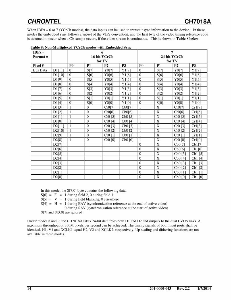
Figure 11: Interlaced PAL Video Timing
INTERVALS
4
3
2
1
BURST BLANKING
START OF
VSYNC
FIELD 4
FIELD 3
FIELD 2
FIELD 1

CHRONTEL CH7018A
201-0000-043 Rev. 2.2, 1/7/2014 21
Color bars :
White
Ye
llow
Cy
an
Ma
gen
ta
Gre
en
Red
Blu
e
Bla
ckColor /Level mA V
Whi te 26.66 1.000
Yellow 24.66 0.925
Cyan 21.37 0.801
Green 19.37 0.726
M agenta 16.22 0.608
Red 14.22 0.533
B lue 11.08 0.415B lac k 9.08 0.340
B lank 7.65 0.287
S ync 0.00 0.000
Figure 12: NTSC Y (Luminance) Output Waveform (DACG = 0)
C olor ba rs:
Wh
ite
Yello
w
Cy
an
Mag
en
ta
Gre
en
Re
d
Blu
e
Bla
ck
C o lor/Level mA V
W hite 26.75 1.003
Yel low 24.62 0.923
C y an 21.11 0.792
G reen 18.98 0.712
M agenta 15.62 0.586
Red 13.49 0.506
Blue 10.14 0.380
B lank/ B lac k 8.00 0.300
Sy nc 0 .00 0.000
Figure 13: PAL Y (Luminance) Video Output Waveform (DACG = 1)
CHRONTEL CH7018A
22 201-0000-043 Rev. 2.2 1/7/2014
Color bars:
Wh
ite
Ye
llow
Cya
n
Ma
gen
ta
Gre
en
Red
Blu
e
Bla
ckColor/Level mA V
Cyan/Red 25.80 0.968
Green/Magenta 25.01 0.938
Yellow/Blue 22.44 0.842
Peak Burst 18.08 0.678
Blank 14.29 0.536
Yellow/Blue 6.15 0.230
Green/Magenta 3.57 0.134
Cyan/Red 2.79 0.105
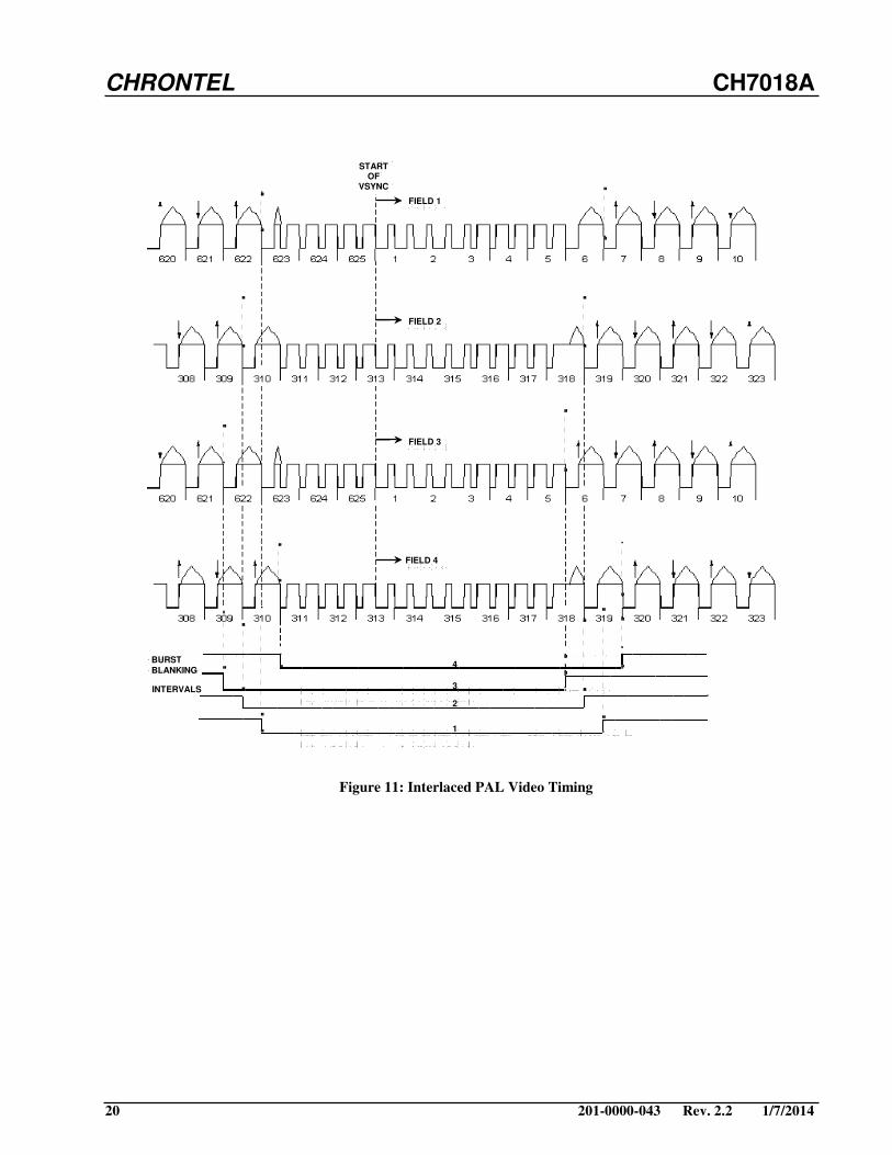
Peak Burst 10.51 0.3943.579545 MHz Color Burst
(9 cycles)
Figure 14: NTSC C (Chrominance) Video Output Waveform (DACG = 0)
Color bars:
Wh
ite
Ye
llow
Cya
n
Ma
gen
ta
Gre
en
Red
Blu
e
Bla
ckColor/Level mA V
Cyan/Red 27.51 1.032
Green/Magenta 26.68 1.000
Yellow/Blue 23.93 0.897
Peak Burst 19.21 0.720
Blank 15.24 0.572
Yellow/Blue 6.56 0.246
Green/Magenta 3.81 0.143
Cyan/Red 2.97 0.111
Peak Burst 11.28 0.4234.433619 MHz Color Burst
(10 cycles)
Figure 15: PAL C (Chrominance) Video Output Waveform (DACG = 1)

CHRONTEL CH7018A
201-0000-043 Rev. 2.2, 1/7/2014 23
Color/Level mA V
Peak Chrome 32.88 1.233
White 26.66 1.000
Sync 0.00 0.000
Peak Burst 11.44 0.429
Black 9.08 0.340
Blank 7.65 0.287
Peak Burst 4.45 0.145
Color bars:
White
Ye
llow
Cy
an
Mag
en
ta
Gre
en
Re
d
Blu
e
Bla
ck
3.579545 MHz Color Burst
(9 cycles)
9.06
3.87
Figure 16: Composite NTSC Video Output Waveform (DACG = 0)
Color/Level mA V
Peak Chrome 33.31 1.249
White 26.75 1.003
Sync 0.00 0.000
Peak Burst 11.97 0.449
Blank/Black 8.00 0.300
Peak Burst 4.04 0.151
Color bars:
Wh
ite
Yello
w
Cya
n
Ma
gen
ta
Gre
en
Red
Blu
e
Bla
ck
4.433619 MHz Color Burst
(10 cycles)
Figure 17: Composite PAL Video Output Waveform (DACG = 1)

CHRONTEL CH7018A
24 201-0000-043 Rev. 2.2 1/7/2014
3.3.5 TV Encoder / Bypass RGB / Component Video Outputs
The four TV encoder DAC outputs in the CH7018A can be switched to two sets of output pins DACA[3:0] and
DACB[3:0] via video switches. This feature facilitates simple connection to two sets of video connectors as listed in
Table 12.
Table 12: TV Output Configurations
Output DACs 2 RCA + 1 S-Video SCART
DACA0 (pin 47) CVBS B
DACA1 (pin 43) Y G
DACA2 (pin 45) C R
DACA3 (pin 41) CVBS CVBS
VGA – Bypass RGB HDTV
DACB0 (pin 46) B Pb
DACB1 (pin 42) G Y
DACB2 (pin 44) R Pr
If the application calls for CVBS/S-video, SCART, RGB and YPrPb to output on the DAC output pins, different
reconstruction filters for each type of signal can be implemented on the breakout cables.
The TV Encoder can be bypassed with input data driving the DACs directly. This mode can go to 165 MP/s. The
CH7018A supports YPrPb output for driving 480i TV sets and SCART RGB for European TV.

CHRONTEL CH7018A
201-0000-043 Rev. 2.2, 1/7/2014 25
3.4 LVDS-Out
Multiplexed input data, sync and clock signals from the graphics controllers input to the CH7018A through one of the
two 12-bit variable voltage input ports, D1[11:0] or D2[11:0]. Non-multiplexed 24-bit input data input through both of
the two input ports. For correct LVDS operation, the input data format must be selected to IDFx=0, 1, 2, 3, 5, 8 or 9.
Note for 24-bit formats, IDF1 must be set equal to IDF2.
If the two 12-bit input ports are driven from different timing generators then data can be sent to both the LVDS data path
and the DACs in the TV data path. The DACs can output these data at 165 M pixels/sec to drive a second CRT monitor.
3.4.1 Single LVDS Channel Signal Mapping
Table 13: Signal Mapping for Single LVDS Channel
18-bit 24-bit SPWG 24-bit OpenLDI
LDC[0](1) R0 R0 R2
LDC[0](2) R1 R1 R3
LDC[0](3) R2 R2 R4
LDC[0](4) R3 R3 R5
LDC[0](5) R4 R4 R6
LDC[0](6) R5 R5 R7
LDC[0](7) G0 G0 G2
LDC[1](1) G1 G1 G3
LDC[1](2) G2 G2 G4
LDC[1](3) G3 G3 G5
LDC[1](4) G4 G4 G6
LDC[1](5) G5 G5 G7
LDC[1](6) B0 B0 B2
LDC[1](7) B1 B1 B3
LDC[2](1) B2 B2 B4
LDC[2](2) B3 B3 B5
LDC[2](3) B4 B4 B6
LDC[2](4) B5 B5 B7
LDC[2](5) HSYNC HSYNC HSYNC
LDC[2](6) VSYNC VSYNC VSYNC
LDC[2](7) DE DE DE
LDC[3](1) R6 R0
LDC[3](2) R7 R1
LDC[3](3) G6 G0
LDC[3](4) G7 G1
LDC[3](5) B6 B0
LDC[3](6) B7 B1
LDC[3](7) RES RES

CHRONTEL CH7018A
26 201-0000-043 Rev. 2.2 1/7/2014
3.4.2 Dual LVDS Channel Signal Mapping
Table 14: Signal Mapping for Dual LVDS Channel
18-bit 24-bit SPWG 24-bit OpenLDI
LDC[0](1) Ro0 Ro0 Ro2
LDC[0](2) Ro1 Ro1 Ro3
LDC[0](3) Ro2 Ro2 Ro4
LDC[0](4) Ro3 Ro3 Ro5
LDC[0](5) Ro4 Ro4 Ro6
LDC[0](6) Ro5 Ro5 Ro7
LDC[0](7) Go0 Go0 Go2
LDC[1](1) Go1 Go1 Go3
LDC[1](2) Go2 Go2 Go4
LDC[1](3) Go3 Go3 Go5
LDC[1](4) Go4 Go4 Go6
LDC[1](5) Go5 Go5 Go7
LDC[1](6) Bo0 Bo0 Bo2
LDC[1](7) Bo1 Bo1 Bo3
LDC[2](1) Bo2 Bo2 Bo4
LDC[2](2) Bo3 Bo3 Bo5
LDC[2](3) Bo4 Bo4 Bo6
LDC[2](4) Bo5 Bo5 Bo7
LDC[2](5) HSYNC HSYNC HSYNC
LDC[2](6) VSYNC VSYNC VSYNC
LDC[2](7) DE DE DE
LDC[3](1) Ro6 Ro0
LDC[3](2) Ro7 Ro1
LDC[3](3) Go6 Go0
LDC[3](4) Go7 Go1
LDC[3](5) Bo6 Bo0
LDC[3](6) Bo7 Bo1
LDC[3](7) RES RES
LDC[4](1) Re0 Re0 Re2
LDC[4](2) Re1 Re1 Re3
LDC[4](3) Re2 Re2 Re4
LDC[4](4) Re3 Re3 Re5
LDC[4](5) Re4 Re4 Re6
LDC[4](6) Re5 Re5 Re7
LDC[4](7) Ge0 Ge0 Ge2
LDC[5](1) Ge1 Ge1 Ge3
LDC[5](2) Ge2 Ge2 Ge4
LDC[5](3) Ge3 Ge3 Ge5
LDC[5](4) Ge4 Ge4 Ge6
LDC[5](5) Ge5 Ge5 Ge7
LDC[5](6) Be0 Be0 Be2
LDC[5](7) Be1 Be1 Be3
LDC[6](1) Be2 Be2 Be4
LDC[6](2) Be3 Be3 Be5
LDC[6](3) Be4 Be4 Be6
LDC[6](4) Be5 Be5 Be7
LDC[6](5) LCTLE 1 HSYNC LCTLE
1
LDC[6](6) LCTLF 1 VSYNC LCTLF
1
LDC[6](7) LA6RL 1 DE LA6RL
1
LDC[7](1) Re6 Re0
LDC[7](2) Re7 Re1
CHRONTEL CH7018A
201-0000-043 Rev. 2.2, 1/7/2014 27
LDC[7](3) Ge6 Ge0
LDC[7](4) Ge7 Ge1
LDC[7](5) Be6 Be0
LDC[7](6) Be7 Be1
LDC[7](7) RES RES
Note:
1. See description for Register 65h. 3.4.3 Panel Fitting Up-Scaler
The Up-scaler in CH7018A supports the following panel sizes:
Table 15: Popular Panel Sizes
UXGA 1600x1200
SXGA+ 1400x1050
1360x1024
SXGA 1280x1024
1280x960
XGA 1024x768
1024x600
SVGA 800x600
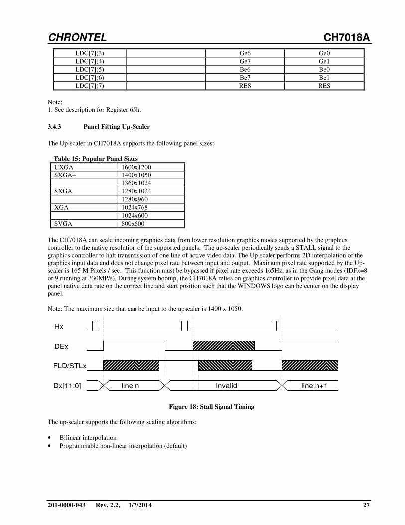
The CH7018A can scale incoming graphics data from lower resolution graphics modes supported by the graphics
controller to the native resolution of the supported panels. The up-scaler periodically sends a STALL signal to the
graphics controller to halt transmission of one line of active video data. The Up-scaler performs 2D interpolation of the
graphics input data and does not change pixel rate between input and output. Maximum pixel rate supported by the Up-
scaler is 165 M Pixels / sec. This function must be bypassed if pixel rate exceeds 165Hz, as in the Gang modes (IDFx=8
or 9 running at 330MP/s). During system bootup, the CH7018A relies on graphics controller to provide pixel data at the
panel native data rate on the correct line and start position such that the WINDOWS logo can be center on the display
panel.
Note: The maximum size that can be input to the upscaler is 1400 x 1050.
Figure 18: Stall Signal Timing
The up-scaler supports the following scaling algorithms:
• Bilinear interpolation
• Programmable non-linear interpolation (default)
line n Invalid line n+1
Hx
DEx
FLD/STLx
Dx[11:0]

CHRONTEL CH7018A
28 201-0000-043 Rev. 2.2 1/7/2014
3.4.4 Dithering
The dither engine in the CH7018A converts 24-bit per pixel to 18-bit per pixel RGB data before sending to the LVDS
encoder. The 1D or the 2D dither algorithm can be selected via serial port programming. Maximum pixel rate supported
is 165 M Pixels / sec. This function must be bypassed when pixel rate exceeds 165MHz.
3.4.5 Power Sequencing
The CH7018A conforms to SPWG’s requirements on power sequencing. The timing specification shown in Figure 19
is a superset of the requirements dictated by the SPWG specification. The timing parameters can be programmed to
different values via the serial port to suit requirements by different panels.
ENAVDD
ENABKL
LVDS Clocks
LVDS Data
T1 T3T2 T4 T5
ENEXBUF
Valid Data
Valid Clock
LVDS_RDY(Internal)
Tristate or GND
Tristate or GND
Figure 19: Power Sequencing
Table 16: Power Sequencing
Range Increment
T1 1-512 ms 1 ms
T2 2-256 ms 2ms
T3 2-256 ms 2ms
T4 1-512 ms 1 ms
T5 0-1600 ms 50ms
Power-on sequence begins when the LVDS software registers are set properly via serial port and the internal PLL lock
detection circuit and the internal Sync detection circuits (See Section 3.4.6) indicate that HSYNC, VSYNC and XCLK
are stable. Note that the BKLEN bit (register 66h) must be set in order for the ENABKL signal to be asserted. Power-off
sequence begins when any detection circuits indicate an instability in the timing signals (See Section 3.4.6), or through
software programming. Once power-off sequence starts, the internal state machine will complete the sequence and
power-on sequence is allowed only after T5 is passed.
When the LVDS output clock and data signals become invalid, these outputs are tri-stated or grounded depending on the
value of the LODP bit.

CHRONTEL CH7018A
201-0000-043 Rev. 2.2, 1/7/2014 29
3.4.6 Panel Protection
The LCD panel can be damaged if HSYNC is absent from the LVDS link. This situation can happen when there is a
catastrophic failure in the PC or the graphics system. The CH7018A is designed to prevent damage to the panel under such a
failure. If the system fails, the CH7018A does not expect any software instruction from the graphics controller to power down
the panel. Detection circuits are used to monitor the three timing signals – HSYNC, VSYNC and XCLK. If any one,
combination of, or all of these signals becomes unstable, the CH7018A will commence Power Down Sequencing according to
section 3.4.5. A description of these detection circuits is shown in Figure 20.
FIFOLOCK
DETECTMUX
PANEN
LSYNCEN
LPLOCK
LPFORC
LPLEN
BKLEN
SYNCST
Register 66h
SYNCDETECT
LSYNCEN
Power Sequencing
FOSC (from oscillator)
LPFORC
LPLEN
0
1
XCLK
UNLOCK
LOCKST
Note:1) LOCKST will be logiclow if either XCLK or the
LVDS PLL output isunstable.2) SYNCST will be logiclow if either Hsync orVsync is unstable ormissing.
LVDS
PLL
ENAVDD
ENABKL
HSYNC
VSYNC
XCLK
Figure 20: Detection Circuits for Panel Protection
A counter is used to count the number of Hsync per frame. If the end counts A, B, and C are the same, CH7018A will
commence Power-Up Sequence. If Hsync is not stable resulting in different end counts, i.e. A is not equal to B or C, then
CH7018A will commence Power-Down Sequence. CH7018A will also go into Power-Down Sequence if Vsync is
missing for 2 frames (D=1) , Hsync is missing for 2 lines (E=1), or XCLK is not stable (F=1). The stability of XCLK is
determined by the number of PLL unlock signals generated within one frame. This number is programmable via serial
port using the BGLMT Register. Under software control, outputs of these detection circuits can be forced to 0 or ignored
by the power sequencing circuits.
3.4.7 EMI Reduction Clock
LVDS data path can support a +- 2.5% EMI reduction clock to reduce EMI emission. The frequency and amplitude of
the EMI reduction triangle waveform can be programmed via the serial port.

CHRONTEL CH7018A
30 201-0000-043 Rev. 2.2 1/7/2014
3.5 Misc. Functions
3.5.1 Voltage Buffering for H and V Syncs
Two 5-volt non-inverting buffers are included so that the graphics controller can output low-voltage Hsync and Vsync
signals to the CH7018A, which in-turn outputs a 5V sync signal to the CRT monitor. Input threshold voltage for these
buffers is programmable via serial port to be equal to VREF2/2.
Figure 21: H and V Sync Buffers
3.5.2 Voltage Translation Buffers
DDC’s for VGA and flat panels are typically terminated into 5V. CH7018A can translate a low-voltage DDC signal into
a 5V DDC signal and vice-versa, eliminating the use of external MOSFET’s for such function.
Figure 22: Voltage Translation Buffers
Graphics Controller CH7017
HOUTVOUT
R,G,B
VGA
Connector
V5V
2 2HIN VIN
VREF2
DD2
DD1DC1
DC2
SDDSDC
5V
(VGA)
(Flat Panel)(Graphics Controller)
VoltageTranslation
1.5V to 3.3V

CHRONTEL CH7018A
201-0000-043 Rev. 2.2, 1/7/2014 31
3.6 Power Down
The CH7018A can be powered down under software control to achieve very low standby current. The matrix in the table
below shows the function of all the power down control bits for the CH7018A. For a complete description of each
individual bit please refer to the appropriate register description in Sections 4.1 and 4.2.
Table 17: Power Down Control Bits
T
V
P
D
D
A
C
P
D
3
D
A
C
P
D
2
D
A
C
P
D
1
D
A
C
P
D
0
L
V
D
S
P
D
L
O
D
P
D
B
1
L
O
D
P
D
B
0
Description
1 X X X X 1 X X Full Power Down
0 1 1 1 0 1 X X TV path powered up, DAC 0 on, DACs 1, 2, 3 off.
LVDS path powered down.
0 0 0 0 1 1 X X TV path powered up, DAC 0 off, DACs 1, 2, 3 on.
LVDS path powered down.
0 0 0 0 0 1 X X TV path powered up, DACs 0, 1, 2, 3 on.
LVDS path powered down
1 X X X X 0 0 0 TV path powered down
LVDS path powered up. Both channels off..
1 X X X X 0 0 1 TV path powered down.
LVDS path powered up. Channel A on, channel B off.
1 X X X X 0 1 0 TV path powered down.
LVDS path powered up. Channel A off, channel B on.
1 X X X X 0 1 1 TV path powered down.
LVDS path powered up. Channel A on, channel B on.
0 0 0 0 0 0 1 1 TV path powered up, DACs 0, 1, 2, 3 on.
LVDS path powered up. Channel A on, channel B on.
Note:
1. X = do not care.
2. TV bit (Register 49h, bit 5) enables the TV path but does not control power down. In order for the TV path to
function, TV must be set to 1 and TVPD set to 0.
3. An input channel which is routing data to an inactive path (TV or LVDS) is automatically powered down. For
example, if PTSEL[1:0] = 10 (D1 input routed to TV and D2 input routed to LVDS) and if TVPD = 1 (TV path
powered down) then data channel D1 is automatically powered down.
4. LDEN[1:0] (Register 73h, bits 4-3) enable the LVDS outputs but do not control power down. In order for an LDVS
channel to be active LVDSPD must be set to 0, the channel must be powered up (LODPDBx=1) and enabled
(LDENx=1).

CHRONTEL CH7018A
32 201-0000-043 Rev. 2.2 1/7/2014
4.0 Register Control
The CH7018A is controlled via a serial control port. The serial bus uses only the SC clock to latch data into Registers,
and does not use any internally generated clocks so that the device can be written to in all Power-Down modes. The
device should retain all Register values during Power-Down modes.
4.1 Non-Macrovision Control Registers Index
The non-Macrovision controls are listed below, divided into four sections: General & Power-Down controls,
Input/Output controls, LVDS controls, TV-Out controls.
GENERAL & POWER DOWN CONTROLS Address
DACPD[3:0] DAC Power Down 49h
DID[7:0] Device ID Register 4Bh
LODPDB[1:0] LVDS Output Driver Power Down control 76h
LSP2 DDC Voltage Translation Buffer select 73h
LVDSPD LVDS Power Down 63h
PANEN Panel Enable (0 – begin Power off sequence, 1 Power-on 66h
RESETIB Software SPP (serial port) reset 48h
RESETDB Software datapath reset 48h
STFDEN[1:0] Enables FLD/STL2 and FLD/STL1 pins 10h
STFDS[1:0] Controls FLD/STL2 and FLD/STL1 output to VGA controller 60h
TPBLD [6:0] Timer – Black Light Disable (T3) 69h
TPBLE [6:0] Timer – Black Light Enable (T2) 68h
TPOFF [8:0] Timer – Power Off (T4) 69h-6Ah
TPON [8:0] Timer - Power On (T1) 67h-68h
TPPWD [5:0] Timer – Power Cycle (T5) 6Bh
TSTP[1:0] Enable/select test pattern generation (color bar, ramp) 48h
TV TV Data and Channel select 49h
TVPD TV Out Power Down 49h
VID[7:0] Version ID Register 4Ah

CHRONTEL CH7018A
201-0000-043 Rev. 2.2, 1/7/2014 33
INPUT/OUTPUT CONTROLS Address
BCO[2:0] Select output signal for BCO pin 22h
BCOEN Enable BCO Output 22h
BCOP BCO polarity 22h
BGBST Bandgap Boost 14h
C3GP[5:0] GPIO Controls 6Eh, 6Dh
C4GP[5:0] GPIO Controls 6Bh-6Dh
C5GP[5:0] GPIO Controls 5Ch, 65h
DACBP DAC bypass 21h
DACG[1:0] DAC gain control 21h
DACT[3:0] DAC termination sense 20h
DES Decode embedded sync (TV-Out data only) 1Fh
GOENB[5:0] Direction control for GPIO pins 1Eh, 6Eh
GPIOL[5:0] Read or Write Data for GPIO pins 1Eh, 6Dh
GPIODR[5:0] GPIO Driver Type – Open Drain or TTL 6Ch
HPIE Hot Plug detect interrupt enable 1Eh
HPIR Hot plug detect interrupt reset 1Eh
HPIS Hot Plug Interrupt Status 20h
HSPTV H sync polarity control TV 1Fh
IBS1 Input buffer type select for D1 1Fh
IBS2 Input Buffer type select for D2 1Ch
IDF1[3:0] Input Data Format for D1 1Fh, 21h
IDF2[3:0] Input Data Format for D2 53h
MCP1 XCLK Polarity Control for D1 1Ch
MCP2 XCLK Polarity Control for D2 1Ch
PCM P-Out 1X, 2X select 1Ch
POUTE P-Out enable 1Eh
POUTP P-Out clock polarity 1Eh
PTSEL[1:0] Control data path from D1 and D2 to TV and/or or LVDS blocks 03h
SENSE TV Sense 20h
SYNCO[1:0] Enables/selects sync output for Scart and bypass modes 21h
SYOTV H/V sync direction control (for TV-Out modes only) 1Fh
VSPTV V sync polarity control for TV 1Fh
XCM1 XCLK 1X / 2X select for D1 1Ch
XCM2 XCLK 1X / 2X select for D2 1Ch
X1CMD[3:0] Delay adjust between XCLK and D1[11:0] 1Dh
X2CMD[3:0] Delay adjust between XCLK and D2[11:0] 53h
XOSC[2:0] Crystal oscillator adjustments 21h, 20h

CHRONTEL CH7018A
34 201-0000-043 Rev. 2.2 1/7/2014
LVDS CONTROLS Address
BGLMT[7:0] Bang Limit control of internal LVDS FIFO over/under run 7Fh
BKLEN Backlight enable 66h
FRSTB FIFO Reset Enable 76h
HAPI[10:0] LVDS Horizontal Active Pixel Input 5Fh - 60h
HAPO[10:0] LVDS Horizontal Active Pixel Output 62h, 63h
HVEN HOUT and VOUT level translators enable 64h
LA3RL OpenLDI Reserved Bit 65h
LA6RL OpenLDI reserved bit 65h
LA7RL OpenLDI reserved bit 65h
LCNTLE OpenLDI Miscellaneous Control Signal 65h
LCNTLF OpenLDI Miscellaneous Control Signal 65h
LDD LVDS Dithering Defeat 64h
LDEN[1:0] LVDS Output Driver enable 73h
LDI OpenLDI specification selection 64h
LDM2D LVDS Dithering Mode – 2D 64h
LEOSWP Odd/even sample output swap on LVDS link 64h
L1ODA[2:0] LVDS Output Driver Amplitude control for bank 1 74h
L2ODA[2:0] LVDS Output Driver Amplitude control for bank 2 74h
LODP LVDS Output Driver Pull-down 74h
LODPE LVDS Output Driver Pre-emphasis 74h
LODST LVDS Output Driver Source Termination control 75h
LPCP[2:0] LVDS PLL Charge pump control 73h
LPFBD[3:0] LVDS PLL feed back divider controls 71h
LPFFD[1:0] LVDS PLL feed forward divider controls 71h
LPLF[4:3] LVDS PLL Loop Filter Capacitor Value 78h
LPLOCK LVDS PLL Lock – read only Register 66h
LPPD[4:0] LVDS PLL phase detector trim 78h
LPPDN LVDS PLL Power Down 76h
LPPRB LVDS PLL Reset 76h
LPPSD[1:0] LVDS PLL post scale divider controls 72h
LPVCO[3:0] LVDS PLL VCO frequency range controls 72h
LSYNCEN Sync Detection Enable 66h
LVDSDC LVDS Dual Channel Select 64h
SYNCST HSYNC and VSYNC stability status 66h
USC[39:0] Up Scaler Coefficients 55h-59h
USHIV [17:0] Up Scaler Horizontal Increment Value 5Ch-5Eh
US Upscaler function enable 63h
USVIV [17:0] Up Scaler Vertical Increment Value 5Ah-5Ch
VALO[10:0] LVDS Vertical Active Line Output 60h, 61h

CHRONTEL CH7018A
201-0000-043 Rev. 2.2, 1/7/2014 35
TV-OUT CONTROLS Address
BL[7:0] TV-Out Black level control 07h
BLKEN Black Level control Register update 1Dh
CBW Chroma video bandwidth 02h
CE[2:0] TV-Out contrast enhancement 08h
CFF[1:0] Chroma flicker filter setting 01h
CFRB Chroma sub-carrier free run (bar) control 02h
CIV[25:0] Calculated sub-carrier increment value read out 10h-13h
CIVC[1:0] Calculated sub-carrier control (hysteresis) 10h
CIVEN Calculated sub-carrier enable (was called ACIV) 10h
CVBW CVBS DAC receives black & white (S-Video) signal 02h
DVS Defeat External Vsync 47h
FSCI[32:0] Sub-carrier generation increment value (when CIVEN=0) 0Ch-0Fh
HP[8:0] TV-Out horizontal position control 05h, 03h
IR[2:0] Input data resolution (when used for TV-Out) 00h
M/S* TV-Out PLL reference input control 1Ch
M[8:0] TV-Out PLL M divider 0Ah, 09h
MEM[2:0] Memory sense amp reference adjust 09h
N[9:0] TV-Out PLL N divider 0Bh, 09h
PALN Select PAL-N when in a CIV mode 10h
PLLCAP TV-Out PLL Capacitor Control 09h
PLLCPI TV-Out PLL Charge Pump control settings 09h
SAV[8:0] Horizontal start of active video 04h, 03h
SR[2:0] TV-Out scaling ratio 00h
TE[2:0] Text enhancement 03h
VBID Vertical blanking interval defeat 02h
VOF[1:0] TV-Out video format (s-video & composite, YPrPb or RGB) 01h
VOS[1:0] TV-Out video standard 00h
VP[8:0] TV-Out vertical position control 06h, 03h
YCV[1:0] Composite video luma bandwidth 02h
YFFH[1:0] Luma text enhancement flicker filter setting 01h
YFFL[1:0] Luma flicker filter setting (incorporates old FLFF control bit) 01h
YSV[1:0] S-Video luma bandwidth 02h

CHRONTEL CH7018A
36 201-0000-043 Rev. 2.2 1/7/2014
Non-Macrovision Control Registers Description
Table 18: Non-Macrovision Serial Port Register Map
Register Bit 7 Bit 6 Bit 5 Bit 4 Bit 3 Bit 2 Bit 1 Bit 0
00h IR2 IR1 IR0 VOS1 VOS0 SR2 SR1 SR0
01h VOF1 VOF0 CFF1 CFF0 YFFH1 YFFH0 YFFL1 YFFL0
02h VBID CFRB CVBW CBW YSV1 YSV0 YCV1 YCV0
03h PTSEL1 PTSEL0 SAV8 HP8 VP8 TE2 TE1 TE0
04h SAV7 SAV6 SAV5 SAV4 SAV3 SAV2 SAV1 SAV0
05h HP7 HP6 HP5 HP4 HP3 HP2 HP1 HP0
06h VP7 VP6 VP5 VP4 VP3 VP2 VP1 VP0
07h BL7 BL6 BL5 BL4 BL3 BL2 BL1 BL0
08h CE2 CE1 CE0
09h MEM2 MEM1 MEM0 N9 N8 M8 PLLCPI PLLCAP
0Ah M7 M6 M5 M4 M3 M2 M1 M0
0Bh N7 N6 N5 N4 N3 N2 N1 N0
0Ch FSCI31 FSCI30 FSCI29 FSCI28 FSCI27 FSCI26 FSCI25 FSCI24
0Dh FSCI23 FSCI22 FSCI21 FSCI20 FSCI19 FSCI18 FSCI17 FSCI16
0Eh FSCI15 FSCI14 FSCI13 FSCI12 FSCI11 FSCI10 FSCI9 FSCI8
0Fh FSCI7 FSCI6 FSCI5 FSCI4 FSCI3 FSCI2 FSCI1 FSCI0
10h STFDEN1 STFDEN0 CIV25 CIV24 CIVC1 CIVC0 PALN CIVEN
11h CIV23 CIV22 CIV21 CIV20 CIV19 CIV18 CIV17 CIV16
12h CIV15 CIV14 CIV13 CIV12 CIV11 CIV10 CIV9 CIV8
13h CIV7 CIV6 CIV5 CIV4 CIV3 CIV2 CIV1 CIV0
14h BGBST
1Ch IBS2 MCP2 XCM2 M/S* MCP1 PCM XCM1
1Dh BLKEN X1CMD3 X1CMD2 X1CMD1 X1CMD0
1Eh GOENB1 GOENB0 GPIOL1 GPIOL0 HPIR HPIE POUTE POUTP
1Fh IBS1 DES SYOTV VSPTV HSPTV IDF12 IDF11 IDF10
20h XOSC2 HPI DACT3 DACT2 DACT1 DACT0 SENSE
21h XOSC1 XOSC0 IDF13 SYNCO1 SYNCO0 DACG1 DACG0 DACBP
22h SHF2 SHF1 SHF0 BCOEN BCOP BCO2 BCO1 BCO0
47h DVS
48h TVPLLR ResetIB ResetDB TSTP1 TSTP0
49h TV DACPD3 DACPD2 DACPD1 DACPD0 TVPD
4Ah VID7 VID6 VID5 VID4 VID3 VID2 VID1 VID0
4Bh DID7 DID6 DID5 DID4 DID3 DID2 DID1 DID0
53h X2CMD3 X2CMD2 X2CMD1 X2CMD0 IDF23 IDF22 IDF21 IDF20
55h USC7 USC6 USC5 USC4 USC3 USC2 USC1 USC0
56h USC15 USC14 USC13 USC12 USC11 USC10 USC9 USC8
57h USC23 USC22 USC21 USC20 USC19 USC18 USC17 USC16
58h USC31 USC30 USC29 USC28 USC27 USC26 USC25 USC24
59h USC39 USC38 USC37 USC36 USC35 USC34 USC33 USC32
5Ah USVIV7 USVIV6 USVIV5 USVIV4 USVIV3 USVIV2 USVIV1 USVIV0
5Bh USVIV15 USVIV14 USVIV13 USVIV12 USVIV11 USVIV10 USVIV8 USVIV8
5Ch C5GP2 C5GP1 C5GP0 USHIV17 USHIV16 USVIV17 USVIV16
5Dh USHIV7 USHIV6 USHIV5 USHIV4 USHIV3 USHIV2 USHIV1 USHIV0
5Eh USHIV15 USHIV14 USHIV13 USHIV12 USHIV11 USHIV10 USHIV9 USHIV8
5Fh HAPI7 HAPI6 HAPI5 HAPI4 HAPI3 HAPI2 HAPI1 HAPI0
60h STFDS1 STFDS0 VALO10 VALO9 VALO8 HAPI10 HAPI9 HAPI8
61h VALO7 VALO6 VALO5 VALO4 VALO3 VALO2 VALO1 VALO0
62h HAPO7 HAPO6 HAPO5 HAPO4 HAPO3 HAPO2 HAPO1 HAPO0
63h US LVDSPD HAPO10 HAPO9 HAPO8
64h HVEN LVDS24 LVDSDC LDD LDM2D LEOSWP LDI
65h C5GP5 C5GP4 C5GP3 LA3RL LA6RL LA7RL LCNTLE LCNTLF
66h SYNCST BKLEN LPLEN LPFORC LPLOCK LSYNCEN PANEN
67h TPON7 TPON6 TPON5 TPON4 TPON3 TPON2 TPON1 TPON0
68h TPON8 TPBLE6 TPBLE5 TPBLE4 TPBLE3 TPBLE2 TPBLE1 TPBLE0
69h TPOFF8 TPBLD6 TPBLD5 TPBLD4 TPBLD3 TPBLD2 TPBLD1 TPBLD0
6Ah TPOFF7 TPOFF6 TPOFF5 TPOFF4 TPOFF3 TPOFF2 TPOFF1 TPOFF0

CHRONTEL CH7018A
201-0000-043 Rev. 2.2, 1/7/2014 37
6Bh C4GP5 C4GP4 TPPWD5 TPPWD4 TPPWD3 TPPWD2 TPPWD1 TPPWD0
6Ch C4GP3 C4GP2 GPIODR5 GPIODR4 GPIODR3 GPIODR2 GPIODR1 GPIODR0
6Dh C4GP1 C4GP0 C3GP5 C3GP4 GPIOL5 GPIOL4 GPIOL3 GPIOL2
6Eh C3GP3 C3GP2 C3GP1 C3GP0 GOENB5 GOENB4 GOENB3 GOENB2
71h LPFFD1 LPFFD0 LPFBD3 LPFBD2 LPFBD1 LPFBD0
72h LPPSD1 LPPSD0 LPVCO3 LPVCO2 LPVCO1 LPVCO0
73h LSP2 DAS1 DAS0 LDEN1 LDEN0 LPCP2 LPCP1 LPCP0
74h LODP LODPE L2ODA2 L2ODA1 L2ODA0 L1ODA2 L1ODA1 L1ODA0
75h LODST
76h FRSTB LPPDN LPPRB LODPDB1 LODPDB0
78h LPLF4 LPLF3 LPPD4 LPPD3 LPPD2 LPPD1 LPPD0
7Fh BGLMT7 BGLMT6 BGLMT5 BGLMT4 BGLMT3 BGLMT2 BGLMT1 BGLMT0

CHRONTEL CH7018A
38 201-0000-043 Rev. 2.2 1/7/2014
4.2 Non-Macrovision Control Registers Description
Display Mode Register Symbol: DM
Address: 00h
Bits: 8
BIT: 7 6 5 4 3 2 1 0
SYMBOL
: IR2 IR1 IR0 VOS1 VOS0 SR2 SR1 SR0
TYPE: R/W R/W R/W R/W R/W R/W R/W R/W
DEFAUL
T: 0 1 1 0 1 0 1 0
Register DM provides programmable control of the CH7018A VGA to TV display mode, including input resolution
(IR[2:0]), video output standard (VOS[1:0]), and scaling ratio (SR[2:0]). The mode of operation is determined according
to Table 19 below. Entries in which the output standard is shown as PAL, PAL-B,D,G,H,I,N,NC can be supported
through proper selection of the chroma sub-carrier. Entries in which the output standard is shown as NTSC, NTSC-M,J
and PAL-M can be supported through proper selection of VOS[1:0] and chroma sub-carrier.
Table 19: Display Modes Mode IR[2:0] VOS
[1:0]
SR[2:0] Input Data
Format
(Active
Video)
Total
Pixels/Line
x Total Lines/Frame
Output
Standard
[TV
Standard]
Scaling Percent
Overscan
Pixel Clock (MHz)
0 000 00 000 512x384 840x500 PAL 5/4 -17 21.000000
1 000 00 001 512x384 840x625 PAL 1/1 -33 26.250000
2 000 01 000 512x384 800x420 NTSC 5/4 0 20.139860
3 000 01 001 512x384 784x525 NTSC 1/1 -20 24.671329
4 001 00 000 720x400 1125x500 PAL 5/4 -13 28.125000
5 001 00 001 720x400 1152x625 PAL 1/1 -30 36.000000
6 001 01 000 720x400 945x420 NTSC 5/4 +4 23.790210
7 001 01 001 720x400 936x525 NTSC 1/1 -16 29.454545
8 010 00 000 640x400 1000x500 PAL 5/4 -13 25.000000
9 010 00 001 640x400 1008x625 PAL 1/1 -30 31.500000
10 010 01 000 640x400 840x420 NTSC 5/4 +4 21.146854
11 010 01 001 640x400 832x525 NTSC 1/1 -17 26.181819
12 010 01 010 640x400 840x600 NTSC 7/8 -27 30.209791
13 011 00 000 640x480 840x500 PAL 5/4 +4 21.000000
14 011 00 001 640x480 840x625 PAL 1/1 -17 26.250000
15 011 00 011 640x480 840x750 PAL 5/6 -30 31.500000
16 011 01 001 640x480 784x525 NTSC 1/1 0 24.671329
17 011 01 010 640x480 784x600 NTSC 7/8 -13 28.195805
18 011 01 011 640x480 800x630 NTSC 5/6 -18 30.209790
19 100 01 001 720x480 882x525 NTSC 1/1 0 27.755245
20 100 01 010 720x480 882x600 NTSC 7/8 -13 31.720280
21 100 01 011 720x480 900x630 NTSC 5/6 -18 33.986015
22 101 00 001 720x576 882x625 PAL 1/1 0 27.562500
23 101 00 011 720x576 900x750 PAL 5/6 -18 33.750000
24 101 00 100 720x576 900x875 PAL 5/7 -30 39.375000
25 110 00 001 800x600 944x625 PAL 1/1 +4 29.500000
26 110 00 011 800x600 960x750 PAL 5/6 -14 36.000000
27 110 00 100 800x600 960x875 PAL 5/7 -27 42.000000
28 110 01 110 800x600 1040x700 NTSC ¾ -6 43.636364
29 110 01 111 800x600 1064x750 NTSC 7/10 -14 47.832169
30 110 01 101 800x600 1040x840 NTSC 5/8 -22 52.363637

CHRONTEL CH7018A
201-0000-043 Rev. 2.2, 1/7/2014 39
31 111 00 100 1024x768 1400x875 PAL 5/7 -4 61.250000
32 111 00 101 1024x768 1400x1000 PAL 5/8 -16 70.000000
33 111 00 110 1024x768 1400x1125 PAL 5/9 -25 78.750000
34 111 01 101 1024x768 1160x840 NTSC 5/8 0 58.405595
35 111 01 110 1024x768 1160x945 NTSC 5/9 -10 65.706295
36 111 01 111 1024x768 1168x1050 NTSC 1 / 2 -20 73.510491
371
101 00 000 720x576 864x625 PAL 1/1 0 13.500000
381
100 01 000 720x480 858x525 NTSC 1/1 0 13.500000
39 001 01 111 720x400 900x441 NTSC 25/21 -1 23.790210
40 010 01 111 640x400 800x441 NTSC 25/21 -1 21.146854
41 011 00 111 640x480 800x525 PAL 25/21 -1 21.000000
42 100 01 101 720x480 880x525 NTSC 1/1 0 27.692308
43 100 01 110 720x480 784x600 NTSC 7/8 -13 28.195805
44 100 01 111 720x480 880x630 NTSC 5/6 -18 33.230770
45 101 00 101 720x576 888x625 PAL 1/1 0 27.750000
46 101 00 110 720x576 880x750 PAL 5/6 -18 33.000000
47 101 00 111 720x576 880x875 PAL 5/7 -30 38.500000 1 These DVD modes operate with interlaced input. Scan conversion and flicker filter are bypassed.
Table 20: Video Output Standard Selection
VOS[1:0] 00 01 10 11
Output Format PAL NTSC PAL-M NTSC-J
Flicker Filter Register Symbol: FF
Address: 01h
Bits: 8
BIT: 7 6 5 4 3 2 1 0
SYMBOL: VOF1 VOF0 CFF1 CFF0 YFFH1 YFFH0 YFFL1 YFFL0
TYPE: R/W R/W R/W R/W R/W R/W R/W R/W
DEFAULT: 0
1 1 0 0 1 1 1
YFFL[1:0] (bits 1-0) of Register FF control the filter used in the scaling and flicker reduction block applied to the non-
text portion (low frequency) of the luminance signal as shown in Table 21 below.
YFFH[1:0] (bits 3-2) of Register FF control the filter used in the scaling and flicker reduction block applied to the text
portion (high frequency) of the luminance signal as shown in Table 21 below.
Table 21: Luma Flicker Filter Control
YFFH and YFFL Flicker Filter Settings (lines)
Scaling Ratio 00 01 10 11
5/4 2 3 3 3
1/1, 7/8, 5/6, 3/4, 5/7, 7/10 2 3 4 5
5/8 2 3 4 6
25/21 2 3 6 6
5/9 3 4 5 6
½ 3 5 5 7

CHRONTEL CH7018A
40 201-0000-043 Rev. 2.2 1/7/2014
CFF[1:0] (bits 5-4) of Register FF control the filter used in the scaling and flicker reduction block applied to the
chrominance signal as shown in Table 22 below. A setting of ‘11’ applies a dot crawl reduction filter which can reduce
the ‘hanging dots’ effect of an NTSC composite video signal when displayed on a TV with a comb filter.
Table 22: Chroma Flicker Filter Control
CFF Flicker Filter Settings (lines)
Scaling Ratio 00 01 10 11
5/4 2 3 3 3
1/1, 7/8, 5/6, 3/4, 5/7, 7/10 2 3 4 5
5/8 2 3 4 5
25/21 2 3 4 6
5/9 3 4 5 6
½ 3 5 5 7
VOF[1:0] (bits 7-6) of Register FF control the video output format. Must be set per the table below:
Table 23: TV Output Configurations
VOF1 VOF0 TV Output Configuration
0 0 YCrCb
0 1 Composite, S-Video
1 0 YPrPb (480I component HDTV set)
1 1 SCART + Composite
For the TV out DAC by-pass for RGB out, refer to DACBP (bit0 of Register 21h).
Refer to Table 12 in Section 3.3.5 for TV Output DAC configuration.
Video Bandwidth Register Symbol: VBW
Address: 02h
Bits: 8
BIT: 7 6 5 4 3 2 1 0
SYMBOL: VBID CFRB CVBW CBW YSV1 YSV0 YCV1 YCV0
TYPE: R/W R/W R/W R/W R/W R/W R/W R/W
DEFAULT: 1 0 0 1 1 1 1 0
YCV[1:0] (bits 1-0) of Register VBW control the filter used to limit the bandwidth of the luma signal in the CVBS
output signal. A table of –3dB bandwidth values is given in Table 24 below.
YSV[1:0] (bits 3-2) of Register VBW control the filter used to limit the bandwidth of the luma signal in the S-Video
output signal. A table of –3dB bandwidth values is given in Table 24 below.
CBW (bit 4) of Register VBW controls the filter used to limit the bandwidth of the chroma signal in the CVBS and S-
Video output signals. A table of –3dB bandwidth values is given in Table 24 below.

CHRONTEL CH7018A
201-0000-043 Rev. 2.2, 1/7/2014 41
Table 24: Video Bandwidth
Mode CBW YSV[1:0] and YCV[1:0] 0 1 00 01 10 11
0 0.620 0.856 2.300 2.690 3.540 5.880
1 0.775 1.070 2.880 3.360 4.430 7.350
2 0.529 0.730 1.960 2.290 3.020 5.010
3 0.648 0.894 2.410 2.810 3.700 6.140
4 0.831 1.150 3.080 3.600 4.750 7.870
5 1.060 1.470 3.950 4.610 6.080 10.100
6 0.703 0.970 2.610 3.040 4.010 6.660
7 0.870 1.200 3.230 3.770 4.970 8.240
8 0.738 1.020 2.740 3.200 4.220 7.000
9 0.930 1.280 3.460 4.030 5.320 8.820
10 0.624 0.862 2.320 2.710 3.570 5.920
11 0.773 1.070 2.870 3.350 4.420 7.330
12 0.892 1.230 3.310 3.870 5.100 8.450
13 0.620 0.856 2.300 2.690 3.540 5.880
14 0.775 1.070 2.880 3.360 4.430 7.350
15 0.930 1.280 3.460 4.030 5.320 8.820
16 0.648 0.894 2.410 2.810 3.700 6.140
17 0.740 1.020 2.750 3.210 4.230 7.010
18 0.793 1.100 2.950 3.440 4.530 7.510
19 0.729 1.010 2.710 3.160 4.160 6.900
20 0.833 1.150 3.090 3.610 4.760 7.890
21 0.892 1.230 3.310 3.870 5.100 8.450
22 0.724 0.999 2.690 3.140 4.130 6.860
23 0.886 1.220 3.290 3.840 5.060 8.400
24 1.030 1.430 3.840 4.480 5.910 9.790
25 0.774 1.070 2.880 3.360 4.430 7.340
26 0.945 1.310 3.510 4.100 5.400 8.960
27 1.100 1.520 4.100 4.780 6.300 10.400
28 0.859 1.190 3.190 3.720 4.910 8.140
29 0.942 1.300 3.500 4.080 5.380 8.920
30 1.030 1.420 3.830 4.470 5.890 9.770
31 0.804 1.110 2.990 3.480 4.590 7.620
32 0.919 1.270 3.410 3.980 5.250 8.710
33 1.030 1.430 3.840 4.480 5.910 9.790
34 0.767 1.060 2.850 3.320 4.380 7.260
35 0.862 1.190 3.200 3.740 4.930 8.170
36 0.965 1.330 3.580 4.180 5.510 9.140
37 0.709 0.979 2.630 3.070 4.050 6.720
38 0.466 0.643 1.730 2.020 2.660 4.410
39 0.703 0.970 2.610 3.040 4.010 6.660
40 0.624 0.862 2.320 2.710 3.570 5.920
41 0.620 0.856 2.300 2.690 3.540 5.880
42 0.727 1.003 2.696 3.153 4.149 6.892
43 0.833 1.150 3.090 3.610 4.760 7.890
44 0.892 1.231 3.309 3.870 5.093 8.459
45 0.728 1.005 2.702 3.160 4.158 6.907
46 0.866 1.196 3.213 3.757 4.945 8.213
47 1.010 1.395 3.748 4.384 5.769 9.582

CHRONTEL CH7018A
42 201-0000-043 Rev. 2.2 1/7/2014
CVBW (bit 5) of Register VBW controls the chroma component of the CVBS signal. CVBW = ‘0’ disables the chroma
signal being added to the CVBS signal, CVBW = ‘1’ enables the chroma signal being added to the CVBS signal.
CFRB (bit 6) of Register VBW controls whether the chroma sub-carrier free-runs, or is locked to the video signal. A ‘1’
causes the sub-carrier to lock to the TV vertical rate, and should be used when the CIVEN bit (Register 10h) is set to ‘0’.
A ‘0’ causes the sub-carrier to free-run, and should be used when the CIVEN bit is set to ‘1’.
VBID (bit 7) of Register VBW controls the vertical blanking interval defeat function. A ‘1’ in this Register location
forces the flicker filter to minimum filtering during the vertical blanking interval. A ‘0’ in this location causes the flicker
filter to remain at the same setting inside and outside of the vertical blanking interval.
Text Enhancement Register Symbol: TE
Address: 03h
Bits: 8
BIT: 7 6 5 4 3 2 1 0
SYMBOL: PTSEL1 PTSEL0 SAV8 HP8 VP8 TE2 TE1 TE0
TYPE: R/W R/W R/W R/W R/W R/W R/W R/W
DEFAULT: 1 0 0 0 0 1 0 1
TE[2:0] (bits 2-0) of Register TE control the text enhancement circuitry within the CH7018A. A value of ‘000’
minimizes the enhancement feature, while a value of ‘111’ maximizes the enhancement.
SAV8, HP8 and VP8 (bits 5-3) of Register TE contain the MSB values for the start of active video, horizontal position
and vertical position controls. They are described in detail in the SAV (address 04h), HP (address 05h) and VP (address
06h) Register descriptions.
PTSEL[1:0] (bits 7-6) of Register TE control the data path from D1[11:0] and D2[11:0] inputs to internal TV and LVDS
blocks. These bits allow one to swap the input data paths to internal TV or LVDS blocks. The default setting which
routes D1 input to TV block and D2 input to LVDS block is recommended.
PTSEL1 PTSEL0 Description
0 0 D1 input is routed to both internal TV and LVDS block
0 1 D1 input is routed to LVDS and D2 input is routed to TV block
1 0 D1 input is routed to TV and D2 input is routed to LVDS block
1 1 D2 input is routed to both internal TV and LVDS block
Start of Active Video Register Symbol: SAV
Address: 04h
Bits: 8
BIT: 7 6 5 4 3 2 1 0
SYMBOL: SAV7 SAV6 SAV5 SAV4 SAV3 SAV2 SAV1 SAV0
TYPE: R/W R/W R/W R/W R/W R/W R/W R/W
DEFAULT: 0 1 0 1 0 0 0 0

CHRONTEL CH7018A
201-0000-043 Rev. 2.2, 1/7/2014 43
Register SAV controls the delay, in pixel increments, from leading edge of horizontal sync to start of active video. The
entire bit field SAV[8:0] is comprised of this Register SAV[7:0], plus SAV[8] contained in the Text Enhancement
Register (03h, bit 5). This is decoded as a whole number of pixels, which can be set anywhere between 0 and 511 pixels.
Therefore, in any 2X clock mode, the number of 2X clocks from the leading edge of Hsync to the first active data must
be a multiple of two clocks.
Horizontal Position Register Symbol: HP
Address: 05h
Bits: 8
BIT: 7 6 5 4 3 2 1 0
SYMBOL: HP7 HP6 HP5 HP4 HP3 HP2 HP1 HP0
TYPE: R/W R/W R/W R/W R/W R/W R/W R/W
DEFAULT: 0 1 0 1 0 0 0 0
Register HP is used to shift the displayed TV image in a horizontal direction (left or right) to achieve a horizontally
centered image on screen. The entire bit field, HP[8:0], is comprised of this Register HP[7:0] plus HP[8] contained in
the Text Enhancement Register (03h, bit 4). Increasing values move the displayed image position right, and decreasing
values move the image position left.
Vertical Position Register Symbol: VP
Address: 06h
Bits: 8
BIT: 7 6 5 4 3 2 1 0
SYMBOL: VP7 VP6 VP5 VP4 VP3 VP2 VP1 VP0
TYPE: R/W R/W R/W R/W R/W R/W R/W R/W
DEFAULT: 0 0 0 0 0 0 0 0
Register VP is used to shift the displayed TV image in a vertical direction (up or down) to achieve a vertically centered
image on screen. The entire bit field, VP[8:0], is comprised of this Register VP[7:0] plus VP[8] contained in the Text
Enhancement Register (03h, bit 3). The value represents the TV line number (relative to the VGA vertical sync) used to
initiate the generation and insertion of the TV vertical interval (i.e. the first sequence of equalizing pulses). Increasing
values delay the output of the TV vertical sync, causing the image position to move up on the TV screen. Decreasing
values, therefore, move the image position DOWN. Each increment moves the image position by one TV line
(approximately 2 input lines). The maximum value that should be programmed into VP[8:0] is the number of TV lines
per field minus one half (262 or 312). When panning the image up, the number should be increased until (TVLPF-1/2) is
reached, the next step should be to reset the Register to zero. When panning the image down the screen, decrement the
VP[8:0] value until the value zero is reached. The next step should set the Register to TVLPF-1/2, and then decrement
for further changes.

CHRONTEL CH7018A
44 201-0000-043 Rev. 2.2 1/7/2014
Black Level Register Symbol: BL
Address: 07h
Bits: 8
BIT: 7 6 5 4 3 2 1 0
SYMBOL: BL7 BL6 BL5 BL4 BL3 BL2 BL1 BL0
TYPE: R/W R/W R/W R/W R/W R/W R/W R/W
DEFAULT: 1 0 0 0 0 0 1 1
Register BL controls the black level. The luminance data is added to this black level, which must be set between 65 and
170. When the input data format is 0 through 3 or 5 the default values are 131 for NTSC and PAL-M, 110 for PAL and
102 for NTSC-J. When the input data format is 4, 6 or 7 the default values are 112 for NTSC and PAL-M, 94 for PAL
and 88 for NTSC-J and YPrPb.
Contrast Enhancement Register Symbol: CE
Address: 08h
Bits: 3
BIT: 7 6 5 4 3 2 1 0
SYMBOL: Reserved Reserved Reserved Reserved Reserved CE2 CE1 CE0
TYPE: R/W R/W R/W R/W R/W R/W R/W R/W
DEFAULT: 0 0 0 0 0 0 1 1
CE[2:0] (bits 2-0) of Register CE control the contrast enhancement feature of the CH7018A, according to Figure 23
below. A setting of ‘0’ results in reduced contrast, a setting of ‘1’ leaves the image contrast unchanged, and values
beyond ‘1’ result in increased contrast. [Note: The straight line denotes Yout = Yin and therefore no enhancement.]
32 36 104 172 240 308 376 444 51232
36
104
172
240
308
376
444
512
< >Yout
in
256
Yinn
Figure 23: Contrast Enhancement of the CH7018A

CHRONTEL CH7018A
201-0000-043 Rev. 2.2, 1/7/2014 45
TV PLL Control Register Symbol: TPC
Address: 09h
Bits: 8
BIT: 7 6 5 4 3 2 1 0
SYMBOL: MEM2 MEM1 MEM0 N9 N8 M8 PLLCPI PLLCAP
TYPE: R/W R/W R/W R/W R/W R/W R/W R/W
DEFAULT: 1 0 0 0 0 0 0 0
PLLCAP (bit 0) of Register TPC controls the TV PLL loop filter capacitor. A recommended listing of PLLCAP settings
versus mode is given in Table 25 below.
Table 25: PLLCAP setting vs. Display Mode
Mode PLLCAP
Value
Mode PLLCAP
Value
0 1 24 1
1 1 25 0
2 0 26 1
3 0 27 1
4 1 28 1
5 1 29 0
6 0 30 1
7 1 31 1
8 0 32 1
9 1 33 1
10 0 34 0
11 1 35 0
12 0 36 0
13 1 37 1
14 1 38 1
15 1 39 0
16 0 40 0
17 0 41 1
18 0 42 0
19 0 43 0
20 0 44 0
21 0 45 0
22 1 46 0
23 1 47 1
PLLCPI (bit 1) of Register TPC should be left at the default value.
M8 and N[9:8] (bits 4-2) of Register TPC contain the MSB values for the TV PLL divider ratio’s. These controls are
described in detail in the PLLM (address 0Ah) and PLLN (address 0Bh) Register descriptions.
MEM[0] (bit 5) of Register TPC controls the input latch bias current level. The default value is recommended.
MEM[2:1] (bits 7-6) of Register TPC control the memory sense amp reference level. The default value is recommended.

CHRONTEL CH7018A
46 201-0000-043 Rev. 2.2 1/7/2014
TV PLL M Value Register Symbol: PLLM
Address: 0Ah
Bits: 8
BIT: 7 6 5 4 3 2 1 0
SYMBOL: M7 M6 M5 M4 M3 M2 M1 M0
TYPE: R/W R/W R/W R/W R/W R/W R/W R/W
DEFAULT: 0 0 1 1 1 1 1 1
Register PLLM controls the division factor applied to the 14.31818MHz frequency reference clock before it is input to
the TV PLL phase detector when the CH7018A is operating in clock master mode. The entire bit field, M[8:0], is
comprised of this Register M[7:0] plus M[8] contained in the TV PLL Control Register (09h, bit2). In slave mode, an
external pixel clock is used instead of the 14.31818MHz frequency reference, but the division factor is also controlled by
M[8:0]. In slave mode, the value of ‘M’ is internally set to 1. A table of values (Table 26) versus display mode is given
following the PLLN Register description.
TV PLL N Value Register Symbol: PLLN
Address: 0Bh
Bits: 8
BIT: 7 6 5 4 3 2 1 0
SYMBOL: N7 N6 N5 N4 N3 N2 N1 N0
TYPE: R/W R/W R/W R/W R/W R/W R/W R/W
DEFAULT: 0 1 1 1 1 1 1 0
Register PLLN controls the division factor applied to the VCO output before being applied to the PLL phase detector,
when the CH7018A is operating in clock master mode. The entire bit field, N[9:0], is comprised of this Register N[7:0]
plus N[9:8] contained in the TV PLL Control Register (09h, bits 3 and 4). In slave mode, the value of ‘N’ is internally
set to 1. The pixel clock generated in clock master modes is calculated according to the equation Fpixel = Fref * [(N+2)
/ (M+2)]. When using a 14.31818MHz frequency reference, the required M and N values for each mode are shown in
Table 26 below:
Table 26: TV PLL M and N values vs. Display Mode
Mode VGA Resolution,
TV Standard,
Scaling Ratio
N
10-bits
(dec)
N
10-bits
(hex)
M
9-bits
(dec)
M
9-bits
(hex)
0 512x384, PAL, 5:4 20 0x14 13 0x0D
1 512x384, PAL, 1:1 9 0x09 4 0x04
2 512x384, NTSC, 5:4 126 0x7E 89 0x59
3 512x384, NTSC, 1:1 110 0x6E 63 0x3F
4 720x400, PAL, 5:4 53 0x35 26 0x1A
5 720x400, PAL, 1:1 86 0x56 33 0x21
6 720x400, NTSC, 5:4 106 0x6A 63 0x3F
7 720x400, NTSC, 1:1 70 0x46 33 0x21
8 640x400, PAL, 5:4 108 0x6C 61 0x3D

CHRONTEL CH7018A
201-0000-043 Rev. 2.2, 1/7/2014 47
Mode VGA Resolution,
TV Standard,
Scaling Ratio
N
10-bits
(dec)
N
10-bits
(hex)
M
9-bits
(dec)
M
9-bits
(hex)
9 640x400, PAL, 1:1 9 0x09 3 0x03
10 640x400, NTSC, 5:4 94 0x5E 63 0x3F
11 640x400, NTSC, 1:1 62 0x3E 33 0x21
12 640x400, NTSC, 7:8 190 0xBE 89 0x59
13 640x480, PAL, 5:4 20 0x14 13 0x0D
14 640x480, PAL, 1:1 9 0x09 4 0x04
15 640x480, PAL, 5:6 9 0x09 3 0x03
16 640x480, NTSC, 1:1 110 0x6E 63 0x3F
17 640x480, NTSC, 7:8 126 0x7E 63 0x3F
18 640x480, NTSC, 5:6 190 0xBE 89 0x59
19 720x480, NTSC, 1:1 124 0x7C 63 0x3F
20 720x480, NTSC, 7:8 142 0x8E 63 0x3F
21 720x480, NTSC, 5:6 214 0xD6 89 0x59
22 720x480, PAL, 1:1 75 0x4B 38 0x26
23 720x480, PAL, 5:6 31 0x1F 12 0x0C
24 720x480, PAL, 5:7 9 0x09 2 0x02
25 800x600, PAL, 1:1 647 0x287 313 0x139
26 800x600, PAL, 5:6 86 0x56 33 0x21
27 800x600, PAL, 5:7 42 0x2A 13 0x0D
28 800x600, NTSC, 3:4 62 0x3E 19 0x13
29 800x600, NTSC, 7:10 302 0x12E 89 0x59
30 800x600, NTSC, 5/8 126 0x7E 33 0x21
31 1024x768, PAL, 5:7 75 0x4B 16 0x10
32 1024x768, PAL, 5:8 42 0x2A 7 0x07
33 1024x768, PAL, 5:9 20 0x14 2 0x02
34 1024x768, NTSC, 5:8 565 0x235 137 0x89
35 1024x768, NTSC, 5:9 333 0x14D 71 0x47
36 1024x768, NTSC, 1:2 917 0x395 177 0xB1
37 720x576, PAL, 1:1 31 0x1F 33 0x21
38 720x480, NTSC, 1:1 31 0x1F 33 0x21
39 720x480, NTSC, 1:1 106 0x6A 63 0x3F
40 640x400, NTSC, 25:21 94 0x5E 63 0x3F
41 640x480, PAL,25:21 20 0x14 13 0x0D
42 720x480, NTSC, 1:1 174 0xAE 89 0x59
43 720x480, NTSC, 7:8 126 0x7E 63 0x3F
44 720x480, NTSC, 5:6 309 0x135 132 0x84
45 720x576, PAL, 1:1 405 0x195 208 0xD0
46 720x576, PAL, 5:6 240 0xF0 103 0x67
47 720x576, PAL, 5:7 119 0x77 43 0x2B

CHRONTEL CH7018A
48 201-0000-043 Rev. 2.2 1/7/2014
Sub-carrier Value Register Symbol: FSCI
Address: 0Ch – 0Fh
Bits: 8 each
BIT: 7 6 5 4 3 2 1 0
SYMBOL: FSCI# FSCI# FSCI# FSCI# FSCI# FSCI# FSCI# FSCI#
TYPE: R/W R/W R/W R/W R/W R/W R/W R/W
DEFAULT:
Registers FSCI contain a 32-bit value which is used as an increment value for the ROM address generation circuitry
when CIVEN=0. The bit locations are specified as follows:
Register Contents
0Ch FSCI[31:24]
0Dh FSCI[23:16]
0Eh FSCI[15:8]
0Fh FSCI[7:0]
When the CH7018A is used in the clock master mode, the tables below should be used to set the FSCI Registers. When
using these values, the CIVEN bit in Register 10h should be set to ‘0’, and the CFRB bit in Register 02h should be set to
‘1’.
Table 27: FSCI Values (525-Line TV-Out Modes)
Mode NTSC “Normal Dot
Crawl”
(dec)
NTSC “Normal Dot
Crawl”
(hex)
NTSC “No Dot
Crawl”
(dec)
NTSC “No Dot
Crawl”
(hex)
PAL-M “Normal Dot
Crawl”
(dec)
PAL-M “Normal Dot
Crawl”
(hex)
2 763,363,328 0x2D800000 763,366,524 0x2D800C7C 762,524,467 0x2D733333
3 623,153,737 0x25249249 623,156,346 0x25249C7A 622,468,953 0x251A1F59
6 574,429,782 0x223D1A56 574,432,187 0x223D23BB 573,798,541 0x2233788D
7 463,962,517 0x1BA78195 463,964,459 0x1BA7892B 463,452,668 0x1B9FB9FC
10 646,233,505 0x2684BDA1 646,236,211 0x2684C833 645,523,358 0x2679E79E
11 521,957,831 0x1F1C71C7 521,960,019 0x1F1C7A53 521,384,251 0x1F13B13B
12 452,363,454 0x1AF684BE 452,365,347 0x1AF68C23 451,866,351 0x1AEEEEEF
16 623,153,737 0x25249249 623,156,346 0x25249C7A 622,468,953 0x251A1F59
17 545,259,520 0x20800000 545,261,803 0x208008EB 544,660,334 0x2076DB6E
18 508,908,885 0x1E555555 508,911,016 0x1E555DA8 508,349,645 0x1E4CCCCD
19 553,914,433 0x21041041 553,916,752 0x21041950 553,305,736 0x20FAC688
20 484,675,129 0x1CE38E39 484,677,158 0x1CE39626 484,142,519 0x1CDB6DB7
21 452,363,454 0x1AF684BE 452,365,347 0x1AF68C23 451,866,351 0x1AEEEEEF
28 469,762,048 0x1C000000 469,764,015 0x1C0007AF 469,245,826 0x1BF81F82
29 428,554,851 0x198B3A63 428,556,645 0x198B4165 428,083,911 0x19840AC7
30 391,468,373 0x17555555 391,470,012 0x17555BBC 391,038,188 0x174EC4EC
34 526,457,468 0x1F611A7C 526,459,671 0x1F612317 525,878,943 0x1F58469F
35 467,962,193 0x1BE48951 467,964,152 0x1BE490F8 467,447,949 0x1BDCB08D
36 418,281,276 0x18EE773C 418,283,027 0x18EE7E13 417,821,626 0x18E773BA
38 569,408,543 0x21F07C1F 569,410,927 0x21F0856F 568,782,819 0x21E6EFE3
39 574,429,782 0x223D1A56 574,432,187 0x223D23BB 573,798,541 0x2233788D
40 646,233,505 0x2684BDA1 646,236,211 0x2684C833 645,523,358 0x2679E79E
42 555,173,329 0x211745D1 555,175,654 0x21174EE6 554,563,249 0x210DF6B1
43 484,675,129 0x1CE38E39 484,677,158 0x1CE39626 484,142,519 0x1CDB6DB7
44 462,644,441 0x1B9364D9 462,646,378 0x1B936C6A 462,136,041 0x1B8BA2E9

CHRONTEL CH7018A
201-0000-043 Rev. 2.2, 1/7/2014 49
Table 28: FSCI Values (625-Line TV-Out Modes)
Mode PAL
“Normal Dot
Crawl”
PAL
“Normal Dot
Crawl”(hex)
PAL-N
“Normal Dot
Crawl”
PAL-N
“Normal Dot
Crawl”(hex)
0 806,021,060 0x300AE7C4 651,209,077 0x26D0A975
1 644,816,848 0x266F1FD0 520,967,262 0x1F0D545E
4 601,829,058 0x23DF2EC2 486,236,111 0x1CFB5FCF
5 470,178,951 0x1C065C87 379,871,962 0x16A462DA
8 677,057,690 0x285B149A 547,015,625 0x209ACBC9
9 537,347,373 0x2007452D 434,139,385 0x19E070F9
13 806,021,060 0x300AE7C4 651,209,077 0x26D0A975
14 644,816,848 0x266F1FD0 520,967,262 0x1F0D545E
15 537,347,373 0x2007452D 434,139,385 0x19E070F9
22 690,875,194 0x292DEB3A 558,179,209 0x21452389
23 564,214,742 0x21A13BD6 455,846,354 0x1B2BF022
24 483,612,636 0x1CD357DC 390,725,446 0x1749FF46
25 645,499,916 0x26798C0C 521,519,134 0x1F15C01E
26 528,951,320 0x1F872818 427,355,957 0x1978EF35
27 453,386,846 0x1B06225E 366,305,106 0x15D55F52
31 621,787,675 0x250FBA1B 502,361,288 0x1DF16CCB
32 544,064,215 0x206DC2D7 439,566,127 0x1A333F2F
33 483,612,636 0x1CD357DC 390,725,446 0x1749FF46
37 705,268,427 0x2A098ACB 569,807,942 0x21F69446
41 806,021,060 0x300AE7C4 651,209,077 0x26D0A975
45 686,207,118 0x28E6B08E 554,407,728 0x210B9730
46 577,037,804 0x2264E5EC 466,206,498 0x1BC9BF22
47 494,603,832 0x1D7B0E38 399,605,570 0x17D17F42
CIV Control Register Symbol: CIVC
Address: 10h
Bits: 8
BIT: 7 6 5 4 3 2 1 0
SYMBOL: STFDEN1 STFDEN0 CIV25 CIV24 CIVC1 CIVC0 PALN CIVEN
TYPE: R/W R/W R R R/W R/W R/W R/W
DEFAULT: 0 0 X X 0 0 0 1
CIVEN (bit 0) of Register CIVC controls whether the FSCI value is used to set the sub-carrier frequency, or the
automatically calculated (CIV) value. When the CIVEN value is ‘1’, the number calculated and present at the CIV
Registers will automatically be used as the increment value for sub-carrier generation. Whenever this bit is set to ‘1’, the
CFRB bit should be set to ‘0’.
PALN (bit 1) of Register CIVC forces the CIV algorithm to generate the PAL-N (Argentina) sub-carrier frequency when
it is set to ‘1’. When this bit is set to ‘0’, the VOS[1:0] value is used by the CIV algorithm to determine which sub-
carrier frequency to generate.
CIVC[1:0] (bits 3-2) of Register CIVC control the hysteresis circuit which is used to calculate the CIV value. The
default value should be used.
CIV[25:24] (bits 5-4) of Register CIVC contain the MSB values for the calculated increment value (CIV) readout. This
is described in detail in the CIV (address 11h-13h) Register description.

CHRONTEL CH7018A
50 201-0000-043 Rev. 2.2 1/7/2014
STFDEN0 (bit6) of Register CIVC enables the FLD/STL1 output on pin 62.
STFDEN0 = 0 => FLD/STL1 pin high impedance
= 1 => Field or stall output depending on the value of the STFDS0 bit in Register 60h, bit 6.
STFDEN1 (bit6) of Register CIVC enables the FLD/STL2 output on pin 105.
STFDEN1 = 0 => FLD/STL2 pin high impedance
= 1 => Field or stall output depending on the value of the STFDS1 bit in Register 60h, bit 7.
Calculated Increment Value Register Symbol: CIV
Address: 11h –13h
Bits: 8 each
BIT: 7 6 5 4 3 2 1 0
SYMBOL: CIV# CIV# CIV# CIV# CIV# CIV# CIV# CIV#
TYPE: R R R R R R R R
DEFAULT: X X X X X X X X
Registers CIV contain the value that was calculated by the CH7018A as the sub-carrier increment value. The entire bit
field, CIV[25:0], is comprised of these three Registers CIV[23:0] plus CIV[25:24] contained in the CIV Control Register
(10h, bits 4 and 5). This value is used when the CIVEN bit is set to ‘1’. The bit locations are specified below.
Register Contents
10h CIV[25:24]
11h CIV[23:16]
12h CIV[15:8]
13h CIV[7:0]
Chroma Boost Register Symbol: CB
Address: 14h
Bits: 1
BIT: 7 6 5 4 3 2 1 0
SYMBOL: BGBST Reserved Reserved Reserved Reserved Reserved Reserved Reserved
TYPE: R/W R/W R/W R/W R/W R/W R/W R/W
DEFAULT: 0 0 0 0 0 0 0 0
BGBST (bit 7) of register CB boost the bandgap voltage which controls the DAC output by 6% when set to 1. This has
the effect of boosting the DAC output by about 6%. The recommended value is 1.

CHRONTEL CH7018A
201-0000-043 Rev. 2.2, 1/7/2014 51
Clock Mode Register Symbol: CM
Address: 1Ch
Bits: 7
BIT: 7 6 5 4 3 2 1 0
SYMBOL: Reserved IBS2 MCP2 XCM2 M/S* MCP1 PCM XCM1
TYPE: R/W R/W R/W R/W R/W R/W R/W R/W
DEFAULT: 0 0 0 0 0 0 0 0
XCM1 (bit 0) of Register CM signifies the XCLK frequency for the D1 input. A value of ‘0’ is used when XCLK1 is at
the pixel frequency (dual edge clocking mode) and a value of ‘1’ is used when XCLK1 is twice the pixel frequency
(single edge clocking mode).
PCM (bit 1) of Register CM controls the P-Out clock frequency. A value of ‘0’ generates a clock output at the pixel
frequency, while a value of ‘1’ generates a clock at twice the pixel frequency.
MCP1 (bit 2) of Register CM controls the phase of the XCLK clock input for the D1 input. A value of ‘1’ inverts the
XCLK signal at the input of the device. This control is used to select which edge of the XCLK signal to use for latching
input data.
M/S* (bit 3) of Register CM controls whether the device operates in master or slave clock mode. In master mode (M/S*
= ‘1’), the 14.31818MHz clock is used as a frequency reference in the TV PLL, and the M and N values are used to
determine the TV PLL’s operating frequency. In slave mode (M/S* = ‘0’) the XCLK input is used as a reference to the
TV PLL. The M and N TV PLL divider values are forced to one.
XCM2 (bit 4) of Register CM signifies the XCLK frequency for the D2 input. A value of ‘0’ is used when XCLK2 is at
the pixel frequency (dual edge clocking mode) and a value of ‘1’ is used when XCLK3 is twice the pixel frequency
(single edge clocking mode).
MCP2 (bit 5) of Register CM controls the phase of the XCLK clock input for the D2 input. A value of ‘1’ inverts the
XCLK signal at the input of the device. This control is used to select which edge of the XCLK signal to use for latching
input data.
IBS2 (bit 6) of Register CM selects the data and clock input buffer type for the D2 data, this bit has to set to “1”
(differential clock and data type).
Input Clock Register Symbol: IC

CHRONTEL CH7018A
52 201-0000-043 Rev. 2.2 1/7/2014
Address: 1Dh
Bits: 5
BIT: 7 6 5 4 3 2 1 0
SYMBOL: Reserved BLKEN Reserved Reserved X1CMD3 X1CMD2 X1CMD1 X1CMD0
TYPE: R/W R/W R/W R/W R/W R/W R/W R/W
DEFAULT: 0 1 0 0 1 0 0 0
X1CMD[3:0] (bits 3-0) of Register IC control the delay applied to the XCLK1 signal before latching input data D1[11:0]
per the following table. 1 unit is approximately 70 ps worst case.
Table 29: Delay applied to XCLK1 before latching input data D1
X1CMD3 X1CMD2 X1CMD1 X1CMD0 Adjust phase of Clock relative to
Data
0 0 0 0 0 unit, XCLK1 ahead of Data
0 0 0 1 1 unit, XCLK1 ahead of Data
0 0 1 0 2 unit, XCLK1 ahead of Data
0 0 1 1 3 unit, XCLK1 ahead of Data
0 1 0 0 4 unit, XCLK1 ahead of Data
0 1 0 1 5 unit, XCLK1 ahead of Data
0 1 1 0 6 unit, XCLK1 ahead of Data
0 1 1 1 7 unit, XCLK1 ahead of Data
1 0 0 0 0 unit, XCLK1 behind Data
1 0 0 1 1 unit, XCLK1 behind Data
1 0 1 0 2 unit, XCLK1 behind Data
1 0 1 1 3 unit, XCLK1 behind Data
1 1 0 0 4 unit, XCLK1 behind Data
1 1 0 1 5 unit, XCLK1 behind Data
1 1 1 0 6 unit, XCLK1 behind Data
1 1 1 1 7 unit, XCLK1 behind Data
BLKEN (bit 6) of Register IC controls the Black Level control Register update during the vertical sync blanking period.
A value of ‘0’ disables the Black Level control Register update. A value of ‘1’ enables the Black Level control Register
update.
GPIO Control Register Symbol: GPIO
Address: 1Eh
Bits: 8
BIT: 7 6 5 4 3 2 1 0
SYMBOL: GOENB1 GOENB0 GPIOL1 GPIOL0 HPIR HPIE POUTE POUTP
TYPE: R/W R/W R/W R/W R/W R/W R/W R/W
DEFAULT: 1 1 1 1 0 0 0 0
POUTP (bit 0) of Register GPIO controls the polarity of the P-Out signal. A value of ‘0’ does not invert the clock at the
output pad.

CHRONTEL CH7018A
201-0000-043 Rev. 2.2, 1/7/2014 53
POUTE (bit 1) of Register GPIO enables the P-Out signal. A value of ‘1’ drives the P-Out clock signal out of the
P-Out pin. A value of ‘0’ disables the P-Out signal.
HPIE (bit 2) of Register GPIO enables the hot plug interrupt detection signal to be output from the HPINT* pin. A value
of ‘1’ allows the hot plug detect circuit to pull the HPINT* pin low when a change of state has taken place on the hot
plug detect pin. A value of ‘0’ disables the interrupt signal.
HPIR (bit 3) of Register GPIO resets the hot plug detection circuitry. A value of ‘1’ causes the CH7018A to release the
HPINT* pin. When a hot plug interrupt is asserted by the CH7018A (HPINT*) the CH7018A driver should read
Register 20h bit 5 to determine the state of the LVDS termination. After having read this bit, the HPIR bit should be set
high to reset the circuitry, and then set low again.
GPIOL[1:0] (bits 5-4) of Register GPIO define the GPIO Read or Write Data bits [1:0]. The entire bit field is made up of
these bits GPIOL[1:0] plus GPIOL[5:2] contained in the GPIO Data Register (address 6Dh, bits 3-0). Refer to the
description of the GPIOD Register (6Dh) for more information.
GOENB[1:0] (bits 7-6) of Register GPIO define the GPIO Direction Control bits [1:0]. The entire bit field is made up of
these bits GOENB[1:0] plus GOENB[5:2] contained in the GPIO Direction Control Register (address 6Eh, bits 3-0).
Refer to the description of the GPIODC Register (6Eh) for more information.
Input Data Format Register Symbol: IDF
Address: 1Fh
Bits: 8
BIT: 7 6 5 4 3 2 1 0
SYMBOL: IBS1 DES SYOTV VSPTV HSPTV IDF12 IDF11 IDF10
TYPE: R/W R/W R/W R/W R/W R/W R/W R/W
DEFAULT: 0
0 0 0 0 0 0 0
IDF1[2:0] (bits 2-0) of Register IDF select the input data format for the D1 input. The entire bit field, IDF1[3:0], is
comprised of this Register IDF1[2:0] plus IDF3 contained in the DAC Control Register (21h, bit5). See Section 3.2 for
a listing of available formats.
HSPTV (bit 3) of Register IDF controls the horizontal sync polarity for TV. A value of ‘0’ defines the horizontal sync to
be active low, and a value of ‘1’ defines the horizontal sync to be active high.
VSPTV (bit 4) of Register IDF controls the vertical sync polarity for TV. A value of ‘0’ defines the vertical sync to be
active low, and a value of ‘1’ defines the vertical sync to be active high.
SYOTV (bit 5) of Register IDF controls the sync direction for TV. A value of ‘0’ defines sync to be input to the
CH7018A, and a value of ‘1’ defines sync to be output from the CH7018A. The CH7018A can only output sync signals
when operating as a VGA to TV encoder, not when operating as an LVDS transmitter.
DES (bit 6) of Register IDF signifies when the CH7018A is to decode embedded sync signals present in the input data
stream instead of using the H and V pins. This feature is only available for input data formats # 4, 6 or 7. A value of ‘0’
selects the H and V pins to be used as the sync inputs, and a value of ‘1’ selects the embedded sync signal.
IBS1 (bit 7) of Register IDF selects the data and clock input buffer type for the D1 data, this bit has to set to “1”
(differential clock and data type).

CHRONTEL CH7018A
54 201-0000-043 Rev. 2.2 1/7/2014
Connection Detect Register Symbol: CD
Address: 20h
Bits: 7 BIT: 7 6 5 4 3 2 1 0
SYMBOL: Reserved XOSC2 HPI DACT3 DACT2 DACT1 DACT0 SENSE
TYPE: R/W R/W R R R R R R/W
DEFAULT: 0 1 X X X X X 0
DACT[3:0] (bits 4-1) and SENSE (bit 0) of Register CD provide a means to sense the connection of a TV to the four
DAC outputs. The status bits, DACT[3:0] correspond to the termination of the four DAC outputs. However, the values
contained in these status bits ARE NOT VALID until a sensing procedure is performed. Use of this Register requires a
sequence of events to enable the sensing of outputs, then reading out the applicable status bits. The detection sequence
works as follows:
1) Set the power management Register (address 49h) to enable all DAC’s.
2) Set the SENSE bit to a 1. This forces a constant output from the DAC’s. Note that during SENSE = 1, these 4
analog outputs are at steady state and no TV synchronization pulses are asserted.
3) Reset the SENSE bit to 0. This triggers a comparison between the voltage present on these analog outputs and the
reference value. During this step, each of the four status bits corresponding to individual DAC outputs will be reset
to “0” if they are NOT CONNECTED.
4) Read the status bits. The status bits, DACT[3:0] now contain valid information which can be read to determine
which outputs are connected to a TV. Again, a “1” indicates a valid connection, a “0” indicates an unconnected
output.
HPI (bit 5) of Register CD can be read at any time to determine the level of the hot plug detect pin. When the hot plug
detect pin changes state, and the LVDS output is selected, the HPINT* output pin will be pulled low signifying a change
in the LVDS termination. At this point, the HPIR bit in Register 1Eh should be set high, then low to reset the hot plug
detect circuit.
XOSC2 (bit 6) of Register CD contains the MSB value for the XOSC (crystal oscillator gain control) word which is
described in detail in the DC (address 21h) Register description.
DAC Control Register Symbol: DC
Address: 21h
Bits: 8
BIT: 7 6 5 4 3 2 1 0
SYMBOL: XOSC1 XOSC0 IDF13 SYNCO1 SYNCO0 DACG1 DACG0 DACBP
TYPE: R/W R/W R/W R/W R/W R/W R/W R/W
DEFAULT: 0 0 0 0 0 0 0 0
DACBP (bit 0) of Register DC selects the DAC bypass mode. A value of ‘1’ outputs the incoming data directly at the
DAC[3:0] outputs for the VGA-Bypass RGB output. For the other TV output modes such as S-Video, RCA, SCART and
480I HDTV, DACBP bit must be set to 0.
DACG[1:0] (bits 2-1) of Register DC control the DAC gain. DACG0 should be set to ‘0’ for NTSC and PAL-M video
standards, and ‘1’ for PAL and NTSC-J video standards. DACG1 should be ‘0’ when the input data format is RGB (IDF
= 0-3, 5, 8 and 9), and ‘1’ when the input data format is YCrCb (IDF = 4, 6 and 7).
SYNCO[1:0] (bits 4-3) of Register DC select the signal to be output from the C/H Sync pin according to Table 30
below.

CHRONTEL CH7018A
201-0000-043 Rev. 2.2, 1/7/2014 55
Table 30: Composite / Horizontal Sync Output
SYNCO[1:0] Composite / Horizontal Sync Output
00 No Output
01 VGA Horizontal Sync
10 TV Composite Sync
11 TV Horizontal Sync
IDF13 (bit 5) of Register DC is the MSB of the IDF1 word which is described in the IDF (address 1Fh) Register
description.
XOSC[1:0] (bits 7-6) of Register DC control the crystal oscillator. The entire bit field, XOSC[2:0], is comprised of
XOSC[1:0] from this Register plus XOSC2 contained in the Connection Detect Register (20h, bit 6).The default value is
recommended.
Buffered Clock Output Register Symbol: BCO
Address: 22h
Bits: 8
BIT: 7 6 5 4 3 2 1 0
SYMBOL: SHF2 SHF1 SHF0 BCOEN BCOP BCO2 BCO1 BCO0
TYPE: R/W R/W R/W R/W R/W R/W R/W R/W
DEFAULT: 0 0 0 0 0 0 0 0
BCO[2:0] (bits 2-0) of Register BCO select the signal output at the BCO pin, according to Table 31 below:
Table 31: BCO Output Signal
BCO[2:0] Buffered Clock Output BCO[2:0] Buffered Clock Output
000 The 14MHz crystal 100 Sine ROM MSB
001 101 Cosine ROM MSB
010 110 VGA Vertical Sync
011 Field ID 111 TV Vertical Sync
BCOP (bit 3) of Register BCO selects the polarity of the BCO output. A value of ‘1’ does not invert the signal at the
output pad.
BCOEN (bit 4) of Register BCO enables the BCO output pin. When BCOEN is high, the BCO pin will output the
selected signal. When BCOEN is low, the BCO pin will be held in tri-state mode.
Defeat External Vsync Register Symbol: DVS
Address: 47h
Bits: 1
BIT: 7 6 5 4 3 2 1 0
SYMBOL: DVS Reserved Reserved Reserved Reserved Reserved Reserved Reserved
TYPE: R/W R/W R/W R/W R/W R/W R/W R/W
DEFAULT: 0 0 0 0 0 0 0 0
DVS (bit 7) of Register DVS defeats the input Vertical SYNC signal going into the VSYNC timing block when set to
‘1’. As a result of this, the internal self generated TV SYNC will be used.

CHRONTEL CH7018A
56 201-0000-043 Rev. 2.2 1/7/2014
Test Pattern Register Symbol: STP
Address: 48h
Bits: 5
BIT: 7 6 5 4 3 2 1 0
SYMBOL: Reserved Reserved TVPLLR
ResetIB ResetDB Reserved TSTP1 TSTP0
TYPE: R/W R/W R/W R/W R/W R/W R/W R/W
DEFAULT: 0 0 0 1 1 0 0 0
TSTP[1:0] (bits 1:0) of Register STP enable and select test pattern generation (color bar, ramp). This test pattern can be
used for both the LVDS output and the TV Output. The pattern generated is determined by the table below:
Table 32: Test Pattern Selection
TSTP1 TSTP0 Test Pattern
0 0 No test pattern – Input data is used
0 1 Color Bars
1 0 Horizontal Luminance Ramp
1 1 Horizontal Luminance Ramp
ResetDB (bit 3) of Register STP resets the datapath. When ResetDB is ‘0’ the datapath is reset. When ResetDB is ‘1’ the
datapath is enabled. The datapath is also reset at power on by an internally generated power-on-reset signal.
ResetIB (bit 4) of Register STP resets all control Registers (addresses 00h – 7Fh). When ResetIB is ‘0’ the control
Registers are reset to the default values. When ResetIB is ‘1’ the control Registers operate normally. The control
Registers are also reset at power on by an internally generated power on reset signal.
TVPLLR (bit 5) of Register STP resets the TV PLL. When TVPLLR is ‘1’ the PLL is reset. When TVPLLR is ‘0’ the
PLL is enabled. The PLL is also reset at power on by an internally generated power-on-reset signal. In addition it can be
reset using the ResetDB bit above.
Power Management Register Symbol: PM
Address: 49h
Bits: 6
BIT: 7 6 5 4 3 2 1 0
SYMBOL: Reserved Reserved TV DACPD3 DACPD2 DACPD1 DACPD0 TVPD
TYPE: R/W R/W R/W R/W R/W R/W R/W R/W
DEFAULT: 0 0 0 0 0 0 0 1
TVPD (bit 0) of Register PM controls the TV Out block power down. When TVPD is ‘0’ the TV block is ON. When
TVPD is ‘1’ the TV block is powered down.
DACPD[3:0] (bits 4:1) of register PM control DAC0 through DAC3 Power Down. DAC0 through DAC3 will be turned
on only if TVPD bit is set to ‘0’. If TVPD bit is set to ‘1’, then DAC0 through DAC3 will be in power down state
regardless of DACPD0 through DACPD3 state.

CHRONTEL CH7018A
201-0000-043 Rev. 2.2, 1/7/2014 57
Table 33: DAC Power Down Control
TVPD DACPD[3:0] Functional Description
0 0000 All DACs on
0 0001 DAC 0 powered down, DACs 1, 2, 3 on
0 0010 DAC 1 powered down, DACs 0, 2, 3 on
0 0100 DAC 2 powered down, DACs 0, 1, 3 on
0 1000 DAC 3 powered down, DACs 0, 1, 2 on
1 xxxx All DACs powered down
TV (bit 5) of register PM enables the TV path. When TV is ‘0’, the TV data path is disabled. When TV is ‘1’ the TV
data path is enabled.
Version ID Register Symbol: VID
Address: 4Ah
Bits: 8
BIT: 7 6 5 4 3 2 1 0
SYMBOL: VID7 VID6 VID5 VID4 VID3 VID2 VID1 VID0
TYPE: R R R R R R R R
DEFAULT: 1 0 0 0 0 0 0 1
Register VID is a read only Register containing the version ID number of the CH7018A family.
Note:
The Current Version ID of CH7018A is 01h.
Device ID Register Symbol: DID
Address: 4Bh
Bits: 8
BIT: 7 6 5 4 3 2 1 0
SYMBOL: DID7 DID6 DID5 DID4 DID3 DID2 DID1 DID0
TYPE: R R R R R R R R
DEFAULT: 0 0 0 1 1
0 1 1
Register DID is a read only Register containing the device ID number of the CH7018A family.
Note:
The Device ID of CH7018A is 1Ah.

CHRONTEL CH7018A
58 201-0000-043 Rev. 2.2 1/7/2014
XCLK and D2 Adjust & IDF2 Symbol: XDIDF2
Address: 53h
Bits: 8
BIT: 7 6 5 4 3 2 1 0
SYMBOL: X2CMD3 X2CMD2 X2CMD1 X2CMD0 IDF23 IDF22 IDF21 IDF20
TYPE: R/W R/W R/W R/W R/W R/W R/W R/W
DEFAULT: 1 0 0 0 0 0 0 0
IDF2[3:0] (bits 3-0) of Register XDIDF2 select the input data format for the D2 input. See Section 3.2 for a listing of
available formats.
X2CMD[3:0] (bits 7-4) of Register XDIDF2 control the delay applied to the XCLK2 signal before latching input data
D2[11:0] per the following table. 1 unit is approximately 70 ps worst case.
Table 34: Delay applied to XCLK2 before latching input data D2
X2CMD3 X2CMD2 X2CMD1 X2CMD0 Adjust phase of Clock relative to Data
0 0 0 0 0 unit, XCLK2 ahead of Data
0 0 0 1 1 unit, XCLK2 ahead of Data
0 0 1 0 2 unit, XCLK2 ahead of Data
0 0 1 1 3 unit, XCLK2 ahead of Data
0 1 0 0 4 unit, XCLK2 ahead of Data
0 1 0 1 5 unit, XCLK2 ahead of Data
0 1 1 0 6 unit, XCLK2 ahead of Data
0 1 1 1 7 unit, XCLK2 ahead of Data
1 0 0 0 0 unit, XCLK2 behind Data
1 0 0 1 1 unit, XCLK2 behind Data
1 0 1 0 2 unit, XCLK2 behind Data
1 0 1 1 3 unit, XCLK2 behind Data
1 1 0 0 4 unit, XCLK2 behind Data
1 1 0 1 5 unit, XCLK2 behind Data
1 1 1 0 6 unit, XCLK2 behind Data
1 1 1 1 7 unit, XCLK2 behind Data
Up Scaler Coefficient Register 0 Symbol: USCR0
Address: 55h
Bits: 8 each
BIT: 7 6 5 4 3 2 1 0
SYMBOL: USC12 USC11 USC10 USC04 USC03 USC02 USC01 USC00
TYPE: R/W R/W R/W R/W R/W R/W R/W R/W
DEFAULT: 0 0 0 0 0 0 0 0
This Register contains the LSB byte of the Up Scaler Coefficient defined by USCR[4:0] in Registers 55h to 59h. There
are eight Up Scaler coefficients (USC7:0) in groups of 5 bits. Register USCR0 contains the entire coefficient USC0[4:0]
and 3 bits from coefficient USC1.
The value of each coefficient should be in 2’s complement format.

CHRONTEL CH7018A
201-0000-043 Rev. 2.2, 1/7/2014 59
Default Up Scaler Coefficient :
USC 8 [39:35] 7[34:30] 6[29:25] 5[24:20] 4[19:15] 3[14:10] 2[9:5] 1[4:0]
Default 8 8 7 4 1 0 0 0
Note: USC0[4:0] must be always zero and the other coefficient values must be between –3 to 11 in 2’s complement
number. The default Up Scaler Coefficient value is for a non-linear interpolation up scaling function.
Up Scaler Coefficient Register 1 Symbol: USCR1
Address: 56h
Bits: 8
BIT: 7 6 5 4 3 2 1 0
SYMBOL: USC30 USC24 USC23 USC22 USC21 USC20 USC14 USC13
TYPE: R/W R/W R/W R/W R/W R/W R/W R/W
DEFAULT: 1 0 0 0 0 0 0 0
This Register contains the second byte of the Up Scaler Coefficient defined by USCR[4:0] in Registers 55h to 59h.
There are eight Up Scaler coefficients ( USC7:0) in groups of 5 bits. Register USCR1 contains the entire coefficient
USC2[4:0], 2 bits from coefficient USC1 and 1 bit from coefficient USC3.
The value of each coefficient should be in 2’s complement format.
The default values of the Up Scaler coefficients are described in the USCR0 Register (address 55h) description.
Up Scaler Coefficient Register 2 Symbol: USCR2
Address: 57h
Bits: 8
BIT: 7 6 5 4 3 2 1 0
SYMBOL: USC43 USC42 USC41 USC40 USC34 USC33 USC32 USC31
TYPE: R/W R/W R/W R/W R/W R/W R/W R/W
DEFAULT: 0 1 0 0 0 0 0 0
This Register contains the third byte of the Up Scaler Coefficient defined by USCR[4:0] in Registers 55h to 59h. There
are eight Up Scaler coefficients ( USC7:0) in groups of 5 bits. Register USCR2 contains 4 bits from coefficient USC3
and 4 bits from coefficient USC4. The value of each coefficient should be in 2’s complement format.
The default values of the Up Scaler coefficients are described in the USCR0 Register (address 55h) description.

CHRONTEL CH7018A
60 201-0000-043 Rev. 2.2 1/7/2014
Up Scaler Coefficient Register 3 Symbol: USCR3
Address: 58h
Bits: 8
BIT: 7 6 5 4 3 2 1 0
SYMBOL: USC61 USC60 USC54 USC53 USC52 USC51 USC50 USC44
TYPE: R/W R/W R/W R/W R/W R/W R/W R/W
DEFAULT: 0 0 0 0 1 1 1 0
This Register contains the fourth byte of the Up Scaler Coefficient defined by USCR[4:0] in Registers 55h to 59h. There
are eight Up Scaler coefficients ( USC7:0) in groups of 5 bits. Register USCR3 contains the entire coefficient
USC5[4:0], 1 bit from coefficient USC4 and 2 bits from coefficient USC6.
The value of each coefficient should be in 2’s complement format.
The default values of the Up Scaler coefficients are described in the USCR0 Register (address 55h) description.
Up Scaler Coefficient Register 4 Symbol: USCR4
Address: 59h
Bits: 8
BIT: 7 6 5 4 3 2 1 0
SYMBOL: USC74 USC73 USC72 USC71 USC70 USC64 USC63 USC62
TYPE: R/W R/W R/W R/W R/W R/W R/W R/W
DEFAULT: 0 1 0 0 0 0 1 0
This Register contains the fifth byte of the Up Scaler Coefficient defined by USCR[4:0] in Registers 55h to 59h. There
are eight Up Scaler coefficients ( USC7:0) in groups of 5 bits. Register USCR4 contains the entire coefficient USC7[4:0]
and 3 bits from coefficient USC6.
The value of each coefficient should be in 2’s complement format.
The default values of the Up Scaler coefficients are described in the USCR0 Register (address 55h) description.
Up Scaler Vertical Increment Value 0 Symbol: USVIV0
Address: 5Ah Bits: 8
BIT: 7 6 5 4 3 2 1 0
SYMBOL: USVIV7 USVIV6 USVIV5 USVIV4 USVIV3 USVIV2 USVIV1 USVIV0
TYPE: R/W R/W R/W R/W R/W R/W R/W R/W
DEFAULT: 0 1 1 1 1 1 1 1
Register USVIV0 defines the Up Scaler Vertical Increment Value bits [7:0]. The entire bit field, USVIV[17:0], is
comprised of this Register USVIV[7:0] plus USVIV[15:8] contained in the Upscaler vertical Increment Value 1 Register
(5Bh) and USVIV[17:16] in the Upscaler Increment Value Register (5Ch).
For computing the value of USVIV[17:0] use following equation below:

CHRONTEL CH7018A
201-0000-043 Rev. 2.2, 1/7/2014 61
USVIV= 2 18
x VALI - 1
VALO - 1
where ( for example, input is 640 x 480 and LVDS panel output is 1024 x 768 )
VALI is the Vertical Active Line Input from a VGA controller (480 in this example).
VALO is the Vertical Active Line Output and is equal to the LVDS vertical resolution (768 in this example).
Refer to Register 60-61h.
USVIV is the Up Scaler Vertical Increment Value which is in an integer number with truncated (do not round
off) decimal (163711 in this example).
Up Scaler Vertical Increment Value 1 Symbol: USVIV1
Address: 5Bh
Bits: 8
BIT: 7 6 5 4 3 2 1 0
SYMBOL: USVIV15 USVIV14 USVIV13 USVIV12 USVIV11 USVIV10 USVIV9 USVIV8
TYPE: R/W R/W
R/W R/W R/W R/W R/W R/W
DEFAULT: 0 1 1 1 1 1 1 1
Register USVIV1 defines the Up Scaler Vertical Increment Value bits [15:8]. The entire bit field, USVIV[17:0], is
comprised of this Register USVIV[15:8] plus USVIV[7:0] contained in the Upscaler Vertical Increment Value 0
Register (5Ah) and USVIV[17:16] in the Upscaler Increment Value Register (5Ch).
For computing the value of USVIV[17:0] refer to the description for Register USVIV0 (address 5Ah).
GPIO Invert Symbol: GPIOINV
Address: 5Ch
Bits: 7
BIT: 7 6 5 4 3 2 1 0
SYMBOL: C5GP2 C5GP1 C5GP0 Reserved USHIV17 USHIV16 USVIV17 USVIV16
TYPE: R/W R/W R/W R/W R/W R/W R/W R/W
DEFAULT: 0 0 0 0 1 0 1 0
USVIV[17:16] (bits 1:0) of Register USIV define the Up Scaler Vertical Increment Value bits [17:16]. The entire bit
field, USVIV[17:0], is comprised of these bits USVIV[17:16] plus USVIV[7:0] contained in the Upscaler Vertical
Increment Value 0 Register (5Ah) and USVIV[15:8] in the Upscaler Vertical Increment Value 1 Register (5Bh).
For computing the value of USVIV[17:0] refer to the description for Register USVIV0 (address 5Ah).
C5GP[2:0] (bits 7-5) of Register GPIOINV define the GPIO C5 Control bits [5:4]. The entire bit field is made up of
these bits C5GP[2:0] plus C5GP[5:3] contained in the LVDS Encoding 2 Register (65h, bits 7-5). Refer to the
description of the LVDSE2 Register (address 65h) for more information.

CHRONTEL CH7018A
62 201-0000-043 Rev. 2.2 1/7/2014
Up Scaler Horizontal Increment Value 0 Symbol: USHIV0
Address: 5Dh
Bits: 8
BIT: 7 6 5 4 3 2 1 0
SYMBOL: USHIV7 USHIV6 USHIV5 USHIV4 USHIV3 USHIV2 USHIV1 USHIV0
TYPE: R/W R/W R/W R/W R/W R/W R/W R/W
DEFAULT: 1 0 0 1 1 1 1 1
Register USHIV0 defines the Up Scaler Horizontal Increment Value bits [7:0]. The entire bit field, USHIV[17:0], is
comprised of these bits USHIV[7:0] plus USHIV[15:8] contained in the Up Scaler Horizontal Increment Value 1
Register (5Eh) and USHIV[17:16] in the Up Scaler Increment Value Register (5Ch).
For computing the value of USHIV[17:0] use following equation below:
USHIV= 2 18
x HAPI - 1
HAPO
where (for example, input is 640 x 480 and LVDS panel output is 1024 x 768 )
HAPI is the Horizontal Active Pixel Input from VGA controller (640 in this example).
HAPO is the Horizontal Active Pixel Output and is equal to LVDS panel horizontal resolution minus one
(1024-1 = 1023 in this example). Refer to Registers 62h-63h.
USHIV is the Up Scaler Horizontal Increment Value which is an integer number with truncated (do not round
off) decimal (163743 in this example)
Up Scaler Horizontal Increment Value 1 Symbol: USHIV1
Address: 5Eh
Bits: 8
BIT: 7 6 5 4 3 2 1 0
SYMBOL: USHIV15 USHIV14 USHIV13 USHIV12 USHIV11 USHIV10 USHIV9 USHIV8
TYPE: R/W R/W R/W R/W R/W R/W R/W R/W
DEFAULT: 0 1 1 1 1 1 1 1
Register USHIV1 defines the Up Scaler Horizontal Increment Value bits [15:8]. The entire bit field, USHIV[17:0], is
comprised of these bits USHIV[15:8] plus USHIV[7:0] contained in the Upscaler Horizontal Increment Value 0 Register
(5Dh) and USHIV[17:16] in the Upscaler Increment Value Register (5Ch).
For computing the value of USHIV[17:0] refer to the description for Register USHIV0 (address 5Dh).

CHRONTEL CH7018A
201-0000-043 Rev. 2.2, 1/7/2014 63
Horizontal Active Pixel Input Symbol: HAPI
Address: 5Fh
Bits: 8
BIT: 7 6 5 4 3 2 1 0
SYMBOL: HAPI7 HAPI6 HAPI5 HAPI4 HAPI3 HAPI2 HAPI1 HAPI0
TYPE: R/W R/W R/W R/W R/W R/W R/W R/W
DEFAULT: 1 0 0 0 0 0 0 0
Register HAPI defines the Horizontal Active Pixel Input value (from a VGA controller) bits [7:0]. The entire bit field,
HAPI[10:0], is comprised of these bits HAPI[7:0] plus HAPI[10:8] contained in the Active Pixel Input and Line Output
Register (60h). For example, if the VGA input resolution is 640 x 480, the value of HAPI[10:0]=280h=640.
Active Pixel Input & Line Output Symbol: APILO
Address: 60h
Bits: 8
BIT: 7 6 5 4 3 2 1 0
SYMBOL: STFDS1 STFDS0 VALO10 VALO9 VALO8 HAPI10 HAPI9 HAPI8
TYPE: R/W R/W R/W R/W R/W R/W R/W R/W
DEFAULT: 1 0 0 1 1 0 1 0
HAPI[10:8] (bits 2-0) of Register APILO define the Horizontal Active Pixel Input value bits [10:8]. The entire bit field,
HAPI[10:0], is comprised of these bits HAPI[10:8] plus HAPI[7:0] contained in the Horizontal Active Pixel Input
Register (address 5Fh). Refer to the description of the HAPI Register (address 5Fh) for more details.
VALO[10:8] (bits 5-3) of Register APILO define the Vertical Active Line Output value bits [10:8]. The entire bit field,
VALO[10:0], is comprised of these bits VALO[10:8] plus VALO[7:0] contained in the Vertical Active Line Output
Register (address 61h). Refer to the description of the VALO Register (address 61h) for more details.
STFDS[1:0] (bits 8-7) of Register APILO control FLD/STL2 and FLD/STL1 output to a VGA controller. These bits can
be programmed to be either a TV field output from the TV encoder or a Stall output from the flat panel Up-Scaler. These
outputs are tri-stated upon power up. A value of ‘1’ allows FLD output. A value of ‘0’ enables STL output. STFDS0
controls FLD/STL1 and STFDS1 controls FLD/STL2 output. Note that the FLD/STLx pins must first be enabled using
the STFDENx bits located in Register 10h, bits 7-6.

CHRONTEL CH7018A
64 201-0000-043 Rev. 2.2 1/7/2014
Vertical Active Line Output Symbol: VALO
Address: 61h
Bits: 8
BIT: 7 6 5 4 3 2 1 0
SYMBOL: VALO7 VALO6 VALO5 VALO4 VALO3 VALO2 VALO1 VALO0
TYPE: R/W R/W R/W R/W R/W R/W R/W R/W
DEFAULT: 0 0 0 0 0 0 0 0
Register VALO defines the Vertical Active Line Output value bits [7:0]. The entire bit field, VALO[10:0], is comprised
of these bits VALO[7:0] plus VALO[10:8] contained in the Active Pixel Input and Line Output Register (60h).
VALO[10:0] is equal to the target LVDS panel vertical resolution. For example, if the LVDS panel resolution is 1024 x
768, the value of VALO[10:0]=300h=768).
Horizontal Active Pixel Output Symbol: HAPO
Address: 62h
Bits: 8
BIT: 7 6 5 4 3 2 1 0
SYMBOL: HAPO7 HAPO6 HAPO5 HAPO4 HAPO3 HAPO2 HAPO1 HAPO0
TYPE: R/W R/W R/W R/W R/W R/W R/W R/W
DEFAULT: 1 1 1 1 1 1 1 1
Register HAPO defines the Horizontal Active Pixel Output value bits [7:0]. The entire bit field, HAPO[10:0], is
comprised of these bits HAPO[7:0] plus HAPO[10:8] contained in the LVDS Test Mode and Horizontal Active Pixel
Output Register (address 63h, bits 2-0). The value of HAPO[10:0] is equal to the target LVDS panel horizontal
resolution minus one. For example, if the target LVDS Panel resolution is 1024 x 768, the value of HAP0[10:0]=3FFh=
(1024-1).
LVDS Power Down Symbol: LPD
Address: 63h
Bits: 5
BIT: 7 6 5 4 3 2 1 0
SYMBOL: US LVDSPD Reserved Reserved Reserved HAPO10 HAPO9 HAPO8
TYPE: R/W R/W R/W R/W R/W R/W R/W R/W
DEFAULT: 0 0 0 0 1 0 1 1
HAPO[10:8] (bits 2-0) of Register LPD define the Horizontal Active Pixel Output value bits [10:8]. The entire bit field,
HAPO[10:0], is comprised of these bits HAPO[10:8] plus HAPO[7:0] contained in the Horizontal Active Pixel Output
Register (62h). Refer to the description of the HAPO Register (address 62h) for more information.
LVDSPD (bit 6) of Register LPD controls the LVDS power down. When LVDSPD is ‘0’ the LVDS path is ON, when
LVDSPD is ‘1’ the LVDS path is powered down.

CHRONTEL CH7018A
201-0000-043 Rev. 2.2, 1/7/2014 65
US (bit 7) of Register LPD enables the up scaler function. When US is ‘0’ the up scaler is disabled, when US is ‘1’ the
up scaler is enabled.
LVDS Encoding 1 Register Symbol: LVDSE1
Address: 64h
Bits: 7
BIT: 7 6 5 4 3 2 1 0
SYMBOL: HVEN Reserved LVDS24 LVDSDC LDD LDM2D LEOSWP LDI
TYPE: R/W R/W R/W R/W R/W R/W R/W R/W
DEFAULT: 0 0 0 0 1 1 0 1
LDI (bit 0) of Register LVDSE1 controls OpenLDI specification selection. A ‘1’ corresponds to OpenLDI, and a ‘0’
corresponds to SPWG. See Section 3.4.1 for more details.
LEOSWP (bit 1) of Register LVDSE1 provides the added flexibility to swap odd/even samples output on the LVDS link.
LDM2D (bit 2) of Register LVDSE1 selects the dithering function to minimize quantization noise by spreading it out
spatially. A ‘1’ turns on the 2D dither function, and a ‘0’ turns off the dither function.
LDD (bit 3) of Register LVDSE1 bypasses the dither function. A ‘1’ bypasses the dither function. A ‘0’ does not bypass
the dither function.
LVDSDC (bit 4) of Register LVDSE1 allows single or dual channel LVDS to be selected. If the bit is 1, dual channel is
selected. If the bit is 0, single channel is selected.
LVDS24 (bit 5) of Register LVDSE1 selects LVDS 24 bit or 18 bit output format. A ‘1’ provides 24- bit output mode
and a ‘ 0’ provides 18- bit output mode.
HVEN (bit 7) of Register LVDSE1 controls HOUT and VOUT output level translators from HIN and VIN respectively.
When HVEN is ‘0’ the level translators are disabled and HOUT and VOUT are in tri-state. When HVEN is ‘1’ the level
translators are enabled.
LVDS Encoding 2 Register Symbol: LVDSE2
Address: 65h
Bits: 8
BIT: 7 6 5 4 3 2 1 0
SYMBOL: C5GP5 C5GP4 C5GP3 LA3RL LA6RL LA7RL LCNTLE LCNTLF
TYPE: R/W R/W R/W R/W R/W R/W R/W R/W
DEFAULT: 0 0 0 0 0 0 0 0
LCNTLF and LCNTLE (bits 1-0) of Register LVDSE2 are OpenLDI miscellaneous control signals, Cntl F and Cntl E,
for the Display Source Serializer respectively. Refer to the OpenLDI specification v0.95. See Section 3.4.2.
LA7RL and LA3RL (bits 4 and 2) of Register LVDSE2 are OpenLDI reserved bits for future use and may take any value
in 24 bit unbalanced dual pixel mode. Refer to the OpenLDI specification v0.95. See Section 3.4.2.
LA6RL (bit 3) of Register LVDSE2 is an OpenLDI reserved bit for future use and may take any value. Refer to the
OpenLDI specification v0.95, P5. See Section 3.4.2.

CHRONTEL CH7018A
66 201-0000-043 Rev. 2.2 1/7/2014
C5GP[5:3] (bits 7-5) of Register LVDSE2 define the GPIO C5 Control bits [5:3]. The entire bit field is made up of these
bits C5GP[5:3] plus C5GP[2:0] contained in the GPIO Invert Register (5Ch, bits 7-5). C5GP[5:0] invert the data output
on the GPIO[5:0] pins when the pins are configured in output mode. When the corresponding GOENB bits
(GOENB[5:0], see GPIODC Register, address 6Eh, bits 3-0 and GPIO Register, address 1Eh, bits 7-6) are ‘0’ and the
corresponding C5GP bits are ‘1’ the values in GPIOL[5:0] are driven out inverted at the corresponding GPIO pins.
LVDS PLL Miscellaneous Control Register Symbol: LPMC
Address: 66h
Bits: 7
BIT: 7 6 3 4 3 2 1 0
SYMBOL: Reserved SYNCST BKLEN LPLEN LPFORC LPLOCK LSYNCEN PANEN
TYPE: R/W R R/W R/W R/W R R/W R/W
DEFAULT: 0 0 0 0 0 0 0 1
The LMPC Register controls panel protection circuits which control the LVDS panel power up and down sequence (refer
to Section 3.4.6 Panel Protection).
PANEN (bit 0) of the LPMC Register controls the LVDS panel enable.
PANEN = 0 => Begin Power off sequence
= 1 => Power-on
LSYNCEN (bit 1) of the LMPC Register controls the Sync Detection Enable for Power Down.
LSYNCEN = 0 => Normal Power down based on abnormal HSYNC and VSYNC detection.
= 1 => Force unstable SYNC state regardless of HSYNC and VSYNC status to initiate Power
Down cycle via SW control.
LPLOCK (bit 2) of the LMPC Register indicates the status of the PLL Lock
LPLOCK = 0 => PLL is not stable.
= 1 => PLL is stable and properly locked.
LPFORC (bit 3) of the LMPC register : Bypass LVDS Lock Detect Sentry
Bit 3 = 0 => Lock detect sentry is active.
= 1 => Lock detect sentry is overridden if LPLEN is set to ‘1’.
LPLEN (bit 4) of the LMPC register controls LVDS PLL Lock Enable between LPLOCK and LPFORC.
LPLEN = 0 => Select LPLOCK (normal operation)
= 1 => Select LPFORC (Lock detect sentry is overridden if LPFORC is set to ‘1’)
BKLEN (bit 5) of the LMPC Register enables the panel backlight.
BKLEN = 0 => Disable Backlight
=1 => Enable Backlight
SYNCST(bit 6) of the LMPC Register is the Hsync and Vsync stability status bit. Refer to Section 3.4.6.
SYNCST = 0 => Hsync or Vsync are not stable
= 1 => Hsync and Vsync are stable
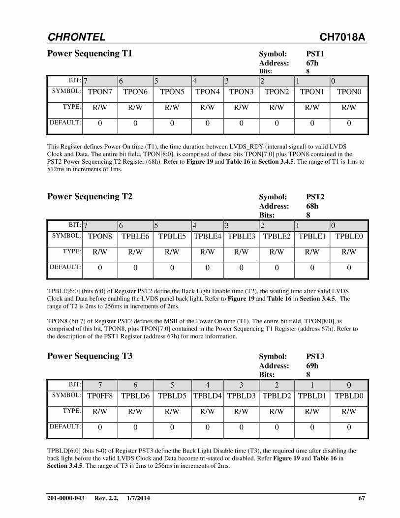
CHRONTEL CH7018A
201-0000-043 Rev. 2.2, 1/7/2014 67
Power Sequencing T1 Symbol: PST1
Address: 67h Bits: 8
BIT: 7 6 5 4 3 2 1 0
SYMBOL: TPON7 TPON6 TPON5 TPON4 TPON3 TPON2 TPON1 TPON0
TYPE: R/W R/W R/W R/W R/W R/W R/W R/W
DEFAULT: 0 0 0 0 0 0 0 0
This Register defines Power On time (T1), the time duration between LVDS_RDY (internal signal) to valid LVDS
Clock and Data. The entire bit field, TPON[8:0], is comprised of these bits TPON[7:0] plus TPON8 contained in the
PST2 Power Sequencing T2 Register (68h). Refer to Figure 19 and Table 16 in Section 3.4.5. The range of T1 is 1ms to
512ms in increments of 1ms.
Power Sequencing T2 Symbol: PST2
Address: 68h
Bits: 8
BIT: 7 6 5 4 3 2 1 0
SYMBOL: TPON8 TPBLE6 TPBLE5 TPBLE4 TPBLE3 TPBLE2 TPBLE1 TPBLE0
TYPE: R/W R/W R/W R/W R/W R/W R/W R/W
DEFAULT: 0 0 0 0 0 0 0 0
TPBLE[6:0] (bits 6:0) of Register PST2 define the Back Light Enable time (T2), the waiting time after valid LVDS
Clock and Data before enabling the LVDS panel back light. Refer to Figure 19 and Table 16 in Section 3.4.5. The
range of T2 is 2ms to 256ms in increments of 2ms.
TPON8 (bit 7) of Register PST2 defines the MSB of the Power On time (T1). The entire bit field, TPON[8:0], is
comprised of this bit, TPON8, plus TPON[7:0] contained in the Power Sequencing T1 Register (address 67h). Refer to
the description of the PST1 Register (address 67h) for more information.
Power Sequencing T3 Symbol: PST3
Address: 69h
Bits: 8
BIT: 7 6 5 4 3 2 1 0
SYMBOL: TP0FF8 TPBLD6 TPBLD5 TPBLD4 TPBLD3 TPBLD2 TPBLD1 TPBLD0
TYPE: R/W R/W R/W R/W R/W R/W R/W R/W
DEFAULT: 0 0 0 0 0 0 0 0
TPBLD[6:0] (bits 6-0) of Register PST3 define the Back Light Disable time (T3), the required time after disabling the
back light before the valid LVDS Clock and Data become tri-stated or disabled. Refer Figure 19 and Table 16 in
Section 3.4.5. The range of T3 is 2ms to 256ms in increments of 2ms.

CHRONTEL CH7018A
68 201-0000-043 Rev. 2.2 1/7/2014
TPOFF8 (bit 7) of Register PST3 defines the MSB of the Power Off time (T4). The entire bit field, TPOFF[8:0], is
comprised of this bit, TPOFF8, plus TPOFF[7:0] contained in the Power Sequencing T4 Register (address 6Ah). Refer
to the description of the PST4 Register (address 6Ah) for more information.
Power Sequencing T4 Symbol: PST4
Address: 6Ah
Bits: 8
BIT: 7 6 5 4 3 2 1 0
SYMBOL: TPOFF7 TPOFF6 TPOFF5 TPOFF4 TPOFF3 TPOFF2 TPOFF1 TPOFF0
TYPE: R/W R/W R/W R/W R/W R/W R/W R/W
DEFAULT: 0 0 0 0 0 0 0 0
Register PST4 defines the Power Off time (T4), the required time prior to power off after the valid LVDS Clock and
Data become tri-stated or disabled. The entire bit field, TPOFF[8:0], is comprised of these bits, TPOFF[7:0], plus
TPOFF8 contained in the Power Sequencing T3 Register (address 69h. Refer to Figure 19 and Table 16 in Section
3.4.5.
The range is 1ms to 512ms in increments of 1ms.
Power Sequencing T5 Symbol: PST5
Address: 6Bh
Bits: 8
BIT: 7 6 5 4 3 2 1 0
SYMBOL: C4GP5 C4GP4 TPPWD5 TPPWD4 TPPWD3 TPPWD2 TPPWD1 TPPWD0
TYPE: R/W R/W R/W R/W R/W R/W R/W R/W
DEFAULT: 1 1 0 0 0 0 0 1
TPPWD[5:0] (bits 5-0) of Register PST5 define the Power Cycle time (T5), the waiting time required prior to enabling
power on after power has been off. Refer to Figure 19 and Table 16 in Section 3.4.5. The range is 0 to 1600ms in
increments of 50ms.
C4GP[5:4] (bits 7-6) of Register PST5 define the GPIO C4 Control bits [5:4]. The entire bit field is made up of these bits
C4GP[5:4] plus C4GP[3:2] contained in the GPIO Driver Type Register (6Ch, bits 7-6) and C4GP[1:0] contained in the
GPIO Data [5:2] Register (6Dh, bits 7-6). Refer to the description of the GPIOD Register (6Dh) for more information.
GPIO Driver Type Symbol: GPIODR
Address: 6Ch
Bits: 8
BIT: 7 6 5 4 3 2 1 0
SYMBOL: C4GP3 C4GP2 GPIODR5 GPIODR4 GPIODR3 GPIODR2 GPIODR1 GPIODR0
TYPE: R/W R/W R/W R/W R/W R/W R/W R/W
DEFAULT: 1 1 1 1 1 1 1 1

CHRONTEL CH7018A
201-0000-043 Rev. 2.2, 1/7/2014 69
GPIODR[5:0] (bits 5:0) of Register GPIODR defines the output driver type for pins GPIO[5:0] – CMOS or Open Drain.
A value of ‘0’ sets corresponding GPIO output to CMOS output type , and a value of ‘1’ sets corresponding GPIO output
to Open Drain type.
C4GP[3:2] (bits 7-6) of Register GPIODR define the GPIO C4 Control bits [3:2]. The entire bit field is made up of these
bits C4GP[3:2] plus C4GP[5:4] contained in the Power Sequencing T5 Register (6Bh, bits 7-6) and C4GP[1:0] contained
in the GPIO Data [5:2] Register (6Dh, bits 7-6). Refer to the description of the GPIOD Register (6Dh) for more
information.
GPIO Data Symbol: GPIOD
Address: 6Dh
Bits: 8
BIT: 7 6 5 4 3 2 1 0
SYMBOL: C4GP1 C4GP0 C3GP5 C3GP4 GPIOL5 GPIOL4 GPIOL3 GPIOL2
TYPE: R/W R/W R/W R/W R/W R/W R/W R/W
DEFAULT: 1 1 0 0 1 1 1 1
GPIOL[5:2] (bits 3-0) of Register GPIOD define the GPIO Read or Write Data bits [5:2]. The entire bit field is made up
of these bits GPIOL[5:2] plus GPIOL[1:0] contained in the GPIO Control Register (1Eh, bits 5-4). GPIOL[5:0] define
the state of the GPIO[5:0] pins in read or write mode.
When the corresponding GOENB bits (GOENB[5:0], see GPIO Control Register, address 1Eh, bits 7-6 and GPIO
Direction Control Register, address 6Eh, bits 3-0) are ‘0’, the values in GPIOL[5:0] are driven out at the corresponding
GPIO pins. When the corresponding GOENB bits are ‘1’, the values in GPIOL[5:0] can be read to determine the level
forced into the corresponding GPIO pins. Note that the default state of GPIOLx depends on the state of the GPIOx pins
since by default these pins are configured as inputs. With no external pullup or pulldown the internal pullup created by
C4GPx being ‘1’ causes GPIOLx to be ‘1’.
When the corresponding GOENB bits are ‘0’ and the corresponding C5GP bits (C5GP[5:0], see GPIOINV Register,
address 5Ch, bits 7-5 and LVDSE2 Register, address 65h, bits 7-5) are ‘1’ the values in GPIOL[5:0] are driven out
inverted at the corresponding GPIO pins.
C3GP[5:4] (bits 5-4) of Register GPIOD define the GPIO C3 Control bits [5:4]. The entire bit field is made up of these
bits C3GP[5:4] plus C3GP[3:0] contained in the GPIO Direction Control Register (6Eh, bits 7-4). C3GP[5:0] control the
weak pull-down (approximately 1MΩ) for the pins GPIO[5:0]. A value of ‘0’ means no pull-down, a value of ‘1’ means
the pull-down is active.
C4GP[1:0] (bits 7-6) of Register GPIOD define the GPIO C4 Control bits [1:0]. The entire bit field is made up of these
bits C4GP[1:0] plus C4GP[5:4] contained in the Power Sequencing T5 Register (6Bh, bits 7-6) and C4GP[3:2] contained
in the GPIO Driver Type Register (6Ch, bits 7-6). C4GP[5:0] control the weak pull-up (approximately 1MΩ) for the pins
GPIO[5:0]. A value of ‘0’ means no pull-up, a value of ‘1’ means the pull-up is active.
GPIO Direction Control Symbol: GPIODC
Address: 6Eh
Bits: 8
BIT: 7 6 5 4 3 2 1 0
SYMBOL: C3GP3 C3GP2 C3GP1 C3GP0 GOENB5 GOENB4 GOENB3 GOENB2
TYPE: R/W R/W R/W R/W R/W R/W R/W R/W
DEFAULT: 0 0 0 0 1 1 1 1

CHRONTEL CH7018A
70 201-0000-043 Rev. 2.2 1/7/2014
GOENB[5:2] (bits 3-0) of Register GPIODC define the GPIO Direction Control bits [5:2]. The entire bit field is made up
of these bits GOENB[5:2] plus GOENB[1:0] contained in the GPIO Control Register (address 1Eh, bits 7-6).
GOENB[5:0] control the direction of the GPIO[5:0] pins. A value of ‘1’ sets the corresponding GPIO pin to an input,
and a value of ‘0’ sets the corresponding pin to a non-inverting output. The level at the output depends on the value of
the corresponding bit GPIOL[5:0]. Refer to the description for the GPIOD Register (address 6Dh) for more information.
C3GP[3:0] (bits 7-4) of Register GPIODC define the GPIO C3 Control bits [3:0]. The entire bit field is made up of these
bits C3GP[3:0] plus C3GP[5:4] contained in the GPIO Data [5:2] Register (6Dh, bits 5-4). Refer to the description of the
GPIOD Register (address 6Dh) for more information.
LVDS PLL Feed Back Divider Control Symbol: LPFBDC
Address: 71h
Bits: 6
BIT: 7 6 5 4 3 2 1 0
SYMBOL: Reserved Reserved LPFFD1 LPFFD0 LPFBD3 LPFBD2 LPFBD1 LPFBD0
TYPE: R/W R/W R/W R/W R/W R/W R/W R/W
DEFAULT: 1 0 1 0 0 0 1 1
LPFBD[3:0] (bits 3-0) of Register LPFBDC define the LVDS PLL Feed-Back Divider Control. The recommended
settings are shown in Table 39 in Section 4.3.
LPFFD[1:0] (bits 5:4) of Register LPFBDC define the LVDS PLL Feed-Forward Divider Control. The recommended
settings are shown in Table 39 in Section 4.3.
LVDS PLL VCO Control Register Symbol: LPVC
Address: 72h
Bits: 6
BIT: 7 6 5 4 3 2 1 0
SYMBOL: Reserved Reserved LPPSD1 LPPSD0 LPVCO3 LPVCO2 LPVCO1 LPVCO0
TYPE: R/W R/W R/W R/W R/W R/W R/W R/W
DEFAULT: 1 0 0 1 0 1 1 0
LPVCO[3:0] (bits 3-0) of Register LPVC determine the LVDS PLL VCO open-loop frequency range. The
recommended settings are shown in Table 39 in Section 4.3.
LPPSD[1:0] (bits 5:4) of Register LPVC define the LVDS PLL post scale divider controls. The recommended settings
are shown in Table 39 in Section 4.3.

CHRONTEL CH7018A
201-0000-043 Rev. 2.2, 1/7/2014 71
Outputs Enable Register Symbol: OUTEN
Address: 73h
Bits: 8
BIT: 7 6 5 4 3 2 1 0
SYMBOL: LSP2 DAS1 DAS0 LDEN1 LDENO LPCP2 LPCP1 LPCP0
TYPE: R/W R/W R/W R/W R/W R/W R/W R/W
DEFAULT: 1 1 0 0 1 0 0 0
LPCP[2:0] (bits 2-0) of Register LPCPC control the LVDS PLL Charge Pump current value. The recommended settings
are shown in Table 39.
LDEN[1:0] (bits 4-3) of Register LPCPC control the output drivers of LVDS output Channel A (LDC[2:0], LDC*[2:0],
LL1C and LL1C*) ,and Channel B ( LDC[6:4], LDC*[6:4], LL2C and LL2C*) per the following table:
Table 35: LVDS Output Drivers Enable
LDEN1 LDEN0 Description
0 0 Both LVDS Channel A and B are Off
0 1 LVDS Channel A is ‘On’ and B is ‘Off’
1 0 LVDS Channel A is ‘Off’ and B is ‘On’
1 1 Both LVDS Channel A and B are ‘On’
DAS[1:0] (bits 6-5) of Register OUTEN control the TV DAC (DACA and DACB ) analog switch per the following
table. Refer also to Table 12: TV Output Configurations.
Table 36: TV DAC Analog Switch Control
DAS1 DAS0 DACA path DACB path
0 0 Off Off
0 1 Off On
1 0 On Off
1 1 On On
LSP2 (bit 7) of Register OUTEN selects the DDC voltage translation buffer output as follows:
LSP2 = 0 => DD1 and DC1 are selected, DD2 and DC2 are not active
= 1 => DD2 and DC2 are selected, DD1 and DC1 are not active
LVDS Output Driver Amplitude control Symbol: LODA
Address: 74h
Bits: 8
BIT: 7 6 5 4 3 2 1 0
SYMBOL: LODP LODPE L2ODA2 L2ODA1 L2ODA0 L1ODA2 L1ODA1 L1ODA0
TYPE: R/W R/W R/W R/W R/W R/W R/W R/W
DEFAULT: 1 1 0 0 0 0 0 0
L1ODA[2:0] (bits 2-0) of Register LODA control the Output Driver Amplitude for LVDS Bank 1. See Table 37 below.
L2ODA[2:0] (bits 5-3) of Register LODA control the Output Driver Amplitude for LVDS Bank 2. See Table 37 below.

CHRONTEL CH7018A
72 201-0000-043 Rev. 2.2 1/7/2014
Table 37: LVDS Output Driver Amplitude
LxODA2 LxODA1 LxODA0 Output Driver Amplitude (mV)
0 0 0 305
0 0 1 285
0 1 0 265
0 1 1 245
1 0 0 225
1 0 1 410
1 1 0 370
1 1 1 330
LODPE (bit 6) of Register LODA controls LVDS Output Driver Pre-Emphasis for both LDC[6:4] and LDC[2:0] by
simultaneous Pull-up and Pull-down diode currents.
LODPE = 0 => Pull up reduced by 33% and pull down reduced by 66%.
= 1 => Default value
LODP (bit 7) of Register LODA activates the LVDS Outputs Driver Pull-Down during power-down.
LODP = 0 => Pull-down devices not active
= 1 => Pull-down devices active
LVDS PLL EMI Reduction Control Symbol: LPSSC
Address: 75h
Bits: 1
BIT: 7 6 5 4 3 2 1 0
SYMBOL: LODST Reserved Reserved Reserved Reserved Reserved Reserved Reserved
TYPE: R/W R/W R/W R/W R/W R/W R/W R/W
DEFAULT: 0 0 0 0 0 0 0 0
LODST (bit 7) of Register LPSSC controls the LVDS Output Drive Source Termination.
LODST = 0 => 100Ω (typ.) shunt disabled between LVDS outputs LDCx and LDCx*, also LLxC and LLxC*
= 1 => 100Ω (typ.) shunt enabled between LVDS outputs LDCx and LDCx*, also LLxC and LLxC*
LVDS Power Down & Loop Filter Resister Symbol: LPDLFR
Address: 76h
Bits: 5
BIT: 7 6 5 4 3 2 1 0
SYMBOL: FRSTB Reserved Reserved Reserved LPPDN LPPRB LODPDB1 LODPDB0
TYPE: R/W R/W R/W R/W R/W R/W R/W R/W
DEFAULT: 1 0 1 0 1 1 0 1
LODPDB[1:0] (bits 1-0) of Register LPDLFR control the LVDS Output Power Down per the following table:

CHRONTEL CH7018A
201-0000-043 Rev. 2.2, 1/7/2014 73
Table 38: LVDS Output Power Down
LODPDB1 LODPDB0 LDC[6:4] & LL2C , LL2C* path LDC[2:0] , LL1C & LL1C* path
0 0 Power Down 1 Power Down
1
0 1 Power Down 1 Power On
1 0 Power On Power Down 1
1 1 Power On Power On
Note 1: Outputs are tri-stated in power down mode unless LODP (address 74h, bit 7) is ‘1’, in which case outputs are
pulled to ground.
LPPRB (bit 2) of Register LPDLFR controls the LVDS PLL Reset.
LPPRB = 0 => LVDS PLL is reset
= 1 => Normal operation
LPPDN (bit 3) of Register LPDLFR controls the LVDS PLL Power Down.
LPPDN = 0 => LVDS PLL is powered down
= 1 => Normal operation
FRSTB (bit 7) of Register LPDLFR controls the FIFO reset.
FRSTB = 0 => Enable FIFO Reset
= 1 => Normal Operation
LVDS Control 2 Symbol: LVCTL2
Address: 78h
Bits: 7
BIT: 7 6 5 4 3 2 1 0
SYMBOL: Reserved LPLF4 LPLF3 LPPD4 LPPD3 LPPD2 LPPD1 LPPD0
TYPE: R/W R/W R/W R/W R/W R/W R/W R/W
DEFAULT: 0 0 1 1 1 0 0 0
LPPD[4:0] (bits 4-0) of Register LVCTL2 define the LVDS PLL Phase Detector Control. The recommended values are
shown in Table 39 in Section 4.3.
LPLF[4:3] (bits 6-5) of Register LVCTL2 control the LVDS PLL Loop Filter Capacitor. The recommended settings are
shown in Table 39.
Bang Limit Control Symbol: BGLMT
Address: 7Fh
Bits: 8
BIT: 7 6 5 4 3 2 1 0
SYMBOL: BGLMT7 BGLMT6 BGLMT5 BGLMT4 BGLMT3 BGLMT2 BGLMT1 BGLMT0
TYPE: R/W R/W R/W R/W R/W R/W R/W R/W
DEFAULT: 0 0 0 1 0 0 0 0
This Register limits the allowable occurrences of internal LVDS FIFO over and under-runs within one VGA frame.

CHRONTEL CH7018A
74 201-0000-043 Rev. 2.2 1/7/2014
4.3 Recommended Settings
The recommended values for the LVDS PLL are shown in Table 39 below.
Table 39: LVDS Divider Control Settings
25MHz to 50MHz operation
Address/Bit 7 6 5 4 3 2 1 0
71h 1 0 1 1 0 1
72h 1 0 0 0 1 1
73h 0 0 0
78h 0 1 0 0 0 0 0
50MHz to 100MHz operation
Address/Bit 7 6 5 4 3 2 1 0
71h 1 0 1 1 0 1
72h 1 0 0 0 1 1
73h 0 0 0
78h 0 1 0 0 0 0 0
100MHz to 160MHz operation (dual panel)
Address/Bit 7 6 5 4 3 2 1 0
71h 1 0 0 0 1 1
72h 1 0 1 1 0 1
73h 0 1 1
78h 1 1 0 0 0 0 0
100MHz to 160MHz operation (single panel)
Address/Bit 7 6 5 4 3 2 1 0
71h 1 0 0 0 1 1
72h 0 1 1 1 0 1
73h 0 1 1
78h 1 1 0 0 0 0 0

CHRONTEL CH7018A
201-0000-043 Rev. 2.2, 1/7/2014 75
5.0 Electrical Specifications
5.1 Absolute Maximum Ratings
Symbol Description Min Typ Max Units
All power supplies relative to GND -0.5 5.0 V
Input voltage of all digital pins GND – 0.5 VDD + 0.5 V
TSC Analog output short circuit duration Indefinite Sec
TSTOR Storage temperature -65 150 °C
TJ Junction temperature 150 °C
Vapor phase soldering (5 second ) 260 °C
Vapor phase soldering (11 second ) 245 °C
TVPS
Vapor phase soldering (60 second ) 225 °C
Note:
1) Stresses greater than those listed under absolute maximum ratings may cause permanent damage to the device.
These are stress ratings only. Functional operation of the device at these or any other conditions above those
indicated under the normal operating condition of this specification is not recommended. Exposure to absolute
maximum rating conditions for extended periods may affect reliability. The temperature requirements of vapor
phase soldering apply to all standard and lead free parts.
2) The device is fabricated using high-performance CMOS technology. It should be handled as an ESD sensitive
device. Voltage on any signal pin that exceeds the power supply voltages by more than ± 0.5V can induce
destructive latchup.
5.2 Recommended Operating Conditions
Symbol Description Min Typ Max Units
TVPLL_VDD TV PLL Digital Power Supply Voltage 3.1 3.3 3.6 V
TVPLL_VCC TV PLL Analog Power Supply Voltage 3.1 3.3 3.6 V
DAC_VDD DAC Power Supply Voltage 3.1 3.3 3.6 V
LPLL_VDD LVDS PLL Power Supply Voltage 3.1 3.3 3.6 V
DVDD Digital Power Supply Voltage 3.1 3.3 3.6 V
LVDD LVDS Power Supply Voltage 3.1 3.3 3.6 V
VDD Generic for all of the above supplies 3.1 3.3 3.6 V
VDDV I/O Power Supply Voltage 1.1 1.8 3.6 V
V5V 5V Supply for H/VOUT 4.75 5 5.25 V
RL Output load to DAC Outputs 37.5 Ω
TAMB Ambient operating temperature (Commercial / Automotive Grade 4)
0 70 °C

CHRONTEL CH7018A
76 201-0000-043 Rev. 2.2 1/7/2014
5.3 Electrical Characteristics (Operating Conditions: TA = 0°°°°C – 70°°°°C, VDD =3.3V ±±±± 5%)
Symbol Description Min Typ Max Units
Video D/A Resolution 10 10 10 bits
Full scale output current 33.9 mA
Video level error 10 %
IVDD Gang Mode @ 165MHz (TV path and upscaler off) 412 mA
IVDD Total supply current 1 DVO input for TV @ 70 MHz 1 DVO input for LVDS @ 165 MHz LVDS output @ 165 MHz (with upscaler)
530 mA
IVDD Total supply current 1 DVO input for TV @ 70 MHz 1 DVO input for LVDS@165 MHz LVDS output @ 165 MHz (w/o upscaler)
400 mA
IVDD Total supply current 1 DVO input for TV @ 70 MHz 1 DVO input for LVDS @ 108MHz LVDS output @ 108 MHz
360 mA
IVDDV VDDV (1.8V) current (15pF load) 4 mA
IPD Total Power Down Current 0.06 mA

CHRONTEL CH7018A
201-0000-043 Rev. 2.2, 1/7/2014 77
5.4 Digital Inputs / Outputs
Symbol Description Test Condition Min Typ Max Unit
VSDOL SPD (serial port data) Output Low Voltage
IOL = 2.0 mA 0.4 V
VSPIH Serial Port (SPC, SPD) Input High Voltage
1.0 VDD + 0.5 V
VSPIL Serial Port (SPC, SPD) Input Low Voltage
GND-0.5 0.4 V
VHYS Hysteresis of Inputs 0.25 V
VDATAIH D[0-11] Input High Voltage Vref1+0.25 DVDD+0.5 V
VDATAIL D[0-11] Input Low Voltage GND-0.5 Vref1-0.25 V
VMISCAIH GPIO, AS, RESET* Input High Voltage
DVDD=3.3V 2.7 VDD + 0.5 V
VMISCAIL GPIO, AS, RESET* Input Low Voltage
DVDD=3.3V GND-0.5 0.6 V
IMISCAPU Pull Up Current (GPIO, AS, RESET*)
VIN = 0V 0.5 5 uA
IMISCAPD Pull Down Current (GPIO)
VIN = 3.3V 0.5 5 uA
VMISCAOH GPIO, ENAVDD, ENABKL, C/HSYNC, BCO/VSYNC, Hx, Vx, HPINTB
Output High Voltage
IOH = -0.4mA VDD-0.2 V
VMISCAOL GPIO, ENAVDD, ENABKL, C/HSYNC, BCO/VSYNC, Hx, Vx, HPINTB
Output Low Voltage
IOL = 3.2mA 0.2 V
VMISCBOH P-OUT, FLD/STL1, FLD/STL2 Output High Voltage
IOH = - 400 uA VDDV-0.2 V
VMISCBOL P-OUT, FLD/STL1, FLD/STL2 Output Low Voltage
IOL = 3.2 mA 0.2 V
VMISCCIH HIN, VIN, HPDET
Input High Voltage DVDD=3.3V 2.7 VDD + 0.5 V
VMISCCIL HIN, VIN, HPDET
Input Low Voltage
DVDD=3.3V GND-0.5 0.6 V
IMISCCPD Pull Down Current
(HIN, VIN, HPDET)
VIN = 3.3V 0.5 5 uA
VMISCDOH HOUT, VOUT
Output High Voltage
V5V = 5V V
VMISCDOL HOUT, VOUT
Output Low Voltage
V5V = 5V V
Note :
VDATA - refers to all digital pixel, clock, data enable and sync inputs.
VMISCA - refers to GPIOx, AS, and RESET* inputs and GPIOx, ENAVDD, ENABKL, C/HSYNC, BCO/VSYNC, HPINTB outputs and Hx, Vx when configured as outputs (SYOTV=1).
IMISCAPD refers to the pulldown current on the GPIOx pins when pull-down is activated. See the description for regieter 6Dh.
VMISCB - refers to P-OUT, FLD/STL1 and FLD/STL2 outputs.
VMISCC - refers to HIN, VIN and HPDET inputs.

CHRONTEL CH7018A
78 201-0000-043 Rev. 2.2 1/7/2014
5.5 AC Specifications
Symbol Description Test Condition Min Typ Max Unit
fXCLK Input (XCLK) frequency 25 165 MHz
tPIXEL Pixel time period 6.06 40 ns
DCXCLK Input (XCLK) Duty Cycle TS + TH < 1.2ns 30 70 %
tXJIT XCLK clock jitter tolerance 2 ns
tS Setup Time: D[11:0], H, V and
DE to XCLK, XCLK* XCLK = XCLK* to
D[11:0], H, V, DE =
Vref1
0.5 ns
tH Hold Time: D[11:0], H, V and
DE to XCLK, XCLK* D[11:0], H, V, DE =
Vref1 to XCLK =
XCLK*
0.5 ns
tR Pout, H and V (when
configured as outputs)
Output Rise Time
(20% - 80%)
15pF load
DVDD, VDDV = 3.3V
1.50 ns
tF Pout, H and V (when
configured as outputs)
Output Fall Time
(20% - 80%)
15pF load
VDDV = 3.3V
1.50 ns
tSTEP De-skew time increment 50 80 ps

CHRONTEL CH7018A
201-0000-043 Rev. 2.2, 1/7/2014 79
5.6 LVDS Output Specifications
The LVDS specifications meet the requirements of ANSI/EIA/TIA-644. Refer to Figure 24 for definitions of parameters.
Symbol Description Test Condition Min Typ Max Unit
| Vt | Steady State Differential Output Magnitude for logic 1
100Ω differential load 247 453 mV
| Vt *| Steady State Differential Output Magnitude for logic 0
100Ω differential load 247 453 mV
| Vt | - | Vt *| Steady State Magnitude of Difference between Logic 1 and 0 Outputs
100Ω differential load 50 mV
|VOS | Steady State Magnitude of
Offset Voltage for Logic 1
Measured at center-
tap of two 50Ω
resistors connected
between outputs
1.125 1.375 V
|VOS* | Steady State Magnitude of
Offset Voltage for Logic 0
Measured at center-
tap of two 50Ω
resistors connected
between outputs
1.125 1.375 V
|VOS | - |VOS* | Steady State Magnitude of
Offset Difference between
Logic States
Measured at center-
tap of two 50Ω
resistors connected
between outputs
50 mV
fLLC LVDS Output Clock
Frequency
25 108 1 MHz
tUI LVDS data unit time interval 25MHz < fLLC <
108MHz
1.3 5.7 ns
tR LVDS data rise time
tUI > 5ns
1.3ns < tUI < 5ns
100Ω and 5pF
differential load
20% -> 80% VSWING
0.3* tUI
1.5
ns
ns
tF LVDS data fall time
tUI > 5ns
1.3ns < tUI < 5ns
100Ω and 5pF
differential load
80% -> 20% VSWING
0.3* tUI
1.5
ns
ns
VRING Voltage ringing after transition 100Ω and 5pF
differential load
20%
VSWING
Note 1: Corresponds to maximum pixel rate fXCLK for single channel operation. Dual channel operation is required for
pixel rates greater than 108MHz.

CHRONTEL CH7018A
80 201-0000-043 Rev. 2.2 1/7/2014
5.7 Timing Information
Note:
In the figures and tables in the following sections XCLK, XCLK*, D[11:0], H, V and DE refer respectively to XCLK1
and XCLK2, XCLK1* and XCLK2*, D1[11:0] and D2[11:0], H1 and H2, V1 and V2, DE1 and DE2.
5.7.1 LVDS Output Timing
tui
tr
tf
Vswing
Vring
+/-20% Vswing
0V Differential
0.8 Vswing
0.2 Vswing
-Vt
+Vt
tj
Figure 24: AC Timing for LVDS Outputs
Table 40: AC Timing for LVDS Outputs
Symbol Parameter Min Typ Max
| Vt | Steady State Differential Output Magnitude see section 5.6
VSWING Voltage Difference between the two Steady State Values of Output
tUi Unit time interval see section 5.6
tr Rise time see section 5.6
tf Fall time see section 5.6
tj Jitter peak to peak1 350ps
Note 1: Maximum jitter with EMI reduction turned off.

CHRONTEL CH7018A
201-0000-043 Rev. 2.2, 1/7/2014 81
5.7.2 Clock-Slave, Sync-Slave Mode
D[11:0]
XCLK
H
V
P0a P0b P1a P1b
DE
64 PIXELS
1 VGA
Line
P2a P2b
XCLK*
t1
t2
t2t2
tS
tH
VIH
VIL
VIH
V IL
VIH
V IL
VIH
VIL
VIH
VIL
VIH
VIL
tS
tS
tH
Figure 25: Timing for Clock-Slave, Sync-Slave Mode
Table 41: Timing for Clock - Slave, Sync - Slave Mode
Symbol Parameter Min Typ Max Unit
tS Setup Time: D[11:0], H, V and DE to XCLK, XCLK* See section 5.5
tH Hold Time: D[11:0], H, V and DE to XCLK, XCLK* See section 5.5
t1 XCLK & XCLK* rise/fall time w/15pF load 1 ns
t2 D[11:0], H, V & DE rise/fall time w/ 15pF load 1 ns

CHRONTEL CH7018A
82 201-0000-043 Rev. 2.2 1/7/2014
5.7.3 Clock-Master, Sync-Slave Mode
D[11:0]
P-OUT
XCLK
H
V
P0a P0b P1a P1b
DE
64 PIXELS
1 VGA
Line
P2a P2b
XCLK*
t1
t2
t2t2
tS
tH
V IH
VIL
VIH
V IL
VIH
VIL
V IH
VIL
VOH
VOL
VIH
VIL
VIH
VIL
tS
tS
tH
tPOUTR
tPOUTF
Figure 26: Timing for Clock-Master, Sync-Slave Mode
Table 42: Timing for Clock - Master, Sync - Slave Mode
Symbol Parameter Min Typ Max Unit
tS Setup Time: D[11:0], H, V and DE to XCLK, XCLK* See section 5.5
tH Hold Time: D[11:0], H, V and DE to XCLK, XCLK* See section 5.5
tR Pout Output Rise Time See section 5.5
tF Pout Output Fall Time See section 5.5
t1 XCLK & XCLK* rise/fall time w/15pF load 1 ns
t2 D[11:0], H, V & DE rise/fall time w/15pF load 1 ns

CHRONTEL CH7018A
201-0000-043 Rev. 2.2, 1/7/2014 83
5.5.3 Clock-Master, Sync-Master Mode
D[11:0]
P-OUT
XCLK
H
V
P0a P0b P1a P1b
DE
64 PIXELS
1 VGA
Line
P2a P2b
XCLK*
t1
tR
t2
tF
tR
tS
tH
t3
VIH
VIL
VIH
V IL
VIH
V IL
VIH
V IL
VOH
VOL
VOH
VOL
VOH
VOL
tS
tF
Figure 27: Clock-Master, Sync-Master Mode
Table 43: Timing for Clock - Master, Sync - Master Mode Symbol Parameter Min Typ Max Unit
tS Setup Time: D[11:0], H, V and DE to XCLK, XCLK* See section 5.5
tH Hold Time: D[11:0], H, V and DE to XCLK, XCLK* See section 5.5
tR Pout, H, V (when configured as outputs) Output Rise Time See section 5.5
tF Pout, H, V (when configured as outputs) Output Fall Time See section 5.5
t1 XCLK & XCLK* rise/fall time w/15pF load 1 ns
t2 D[11:0] & DE rise/fall time w/15pF load 1 ns
t3 Hold time: P-OUT to HSYNC, VSYNC delay 1.5 ns

CHRONTEL CH7018A
84 201-0000-043 Rev. 2.2 1/7/2014
6.0 Package Dimensions
B1
A1
B2A2
C D
I
H
J
G
EF
.004
LEAD
1
38
39 64
65
102
103128
Table of Dimensions
SYMBOL No. of Leads
A1 A2 B1 B2 C D E F G H I J
128 (14X20)
MIN 0.17 1.35 0.05 0.45 0.09 0° Milli- meters MAX
16 22 14 20 0.50 0.27 1.45 0.15
1.00 0.75 0.20 7°
Notes:
1. Conforms to JEDEC standard JESD-30 MS-026D.
2. Dimension B: Top Package body size may be smaller than bottom package size by as much as 0.15 mm.
Dimension B does not include allowable mold protrusions up to 0.25 mm per side.

CHRONTEL CH7018A
201-0000-043 Rev. 2.2, 1/7/2014 85
7.0 Revision History Rev. # Date Section Description
1.0 1/12/02 Package Diagram
Pin Definition
Change package to 14x20 LQFP, removed BGA.
New pin number assignments.
VREF2 definition Set threshold for HIN, VIN, SPC, SPD, SDC & SDD
5.15.1 Updated register map and added index.
5.35.3 Added registers 77h – 7Fh
all Multiple corrections and clarifications.
3 Added TV-Out descriptions.
all Moved package description to section 5. Corrections. Added table
numbers.
6.0 Inserted electrical specs and timing diagrams
Table 20 and 21 Added entries for 25/21 scaling
Table 18 Added foot-note 1
1.1 5/24/02 Register 20h Corrected description of DAC connect detect.
Register 50h Correct description of USMBS[4:0]
3.2.1 Corrected Table 6 in P0a, P0b and P1a columns
3.2.2 Corrected Table 8 in both P0 columns
3.4.2 Corrected Table 14 on 24-Bit OpenLDI column
Register 54h Corrected bit assignment for IBAB[1:0]
Register 64h Name correction: DVDSDC changed to LVDSDC
Register 76h Correct headings in Table 44.
Corrected default bit settings in registers 00h, 65h, 74h, 7Fh
5.4 and 5.5 References to Vref corrected to Vref1.
5.5.2 and 5.5.3 Correct DS to DE in figures
Register 66h Swapped polarity of LPLOCK
Register 79h and 7Ah Rearranged LPVCO[11:8] to match design.
3.4.5 Added note about BKLEN affect on ENABKL to second paragraph.
1.2 7/04/02 Register 64h Changed descriptions for LDD and LDM2D bits.
3.3.4 Corrected Note 1 in Table 11
4.2 Added register 7Fh to customer accessible register list
Register 63h Changed name and symbol.
Register 73h Changed name and symbol
3.4.2 Corrected bit setting for 18bit and 24bit LDI modes and added note 1.
1.3 9/23/02 Register 48h Added TVPLLR bit to reset TV PLL.
Register 10h Added 2 bits to enable FLD/STLx pins.
2.2 Changed descriptions of the SPC, SPD and VREF2 pins
Register 76h LODPD bits name corrected to LODPDB (active low).
Register 11h-13h Changed to read only
Table 26, 26, 27 Added hex values
Register 5Ch Renamed register to GPIO Invert (GPIOINV)
0 Changed VIH and VIL. Added hysteresis. Corrected test condition for
VP-OUTOH . Changed IMISCAPU and added additional outputs to spec. –
FLD/STL1, FLD/STL2, C/HSYNC and BCO/VSYNC.
Swapped descriptions for modes 8 and 9
Register 02h Changed default value for bit 7 (VBID).
Register 10h –13h Changed CIV bits to read only
Registers 1Eh and
6Dh
Changed default value and description of GPIOLx bits.
1.4 2/06/03 4.1 Changed reference to ACIV to CIVEN.
All Changed all references of DVDDV to VDDV
4.1 Moved LPLOCK and LSYNCEN in the Control Register Index from
“Input/Output Controls” to “LVDS Controls”
Various Updated Figure 20 and Table 26 - Corrected N value for mode 11
from 64 to 62.

CHRONTEL CH7018A
86 201-0000-043 Rev. 2.2 1/7/2014
Rev. # Date Section Description
All Updated Section 5.5, tables 42-44 on Timings for Clock.
1.5 6/13/03 Register 07h Updated max and min range for black level pedestal.
6/13/03 5.4, 5.5, and 5.6 Updated section 5.4. Added AC specifications to section 5.5.
Changed format to section 5.6.
1.6 1/19/04 Table 27 Mode 42 values have been updated
5.6, 5.7.1, Table 42 Added section 5.6, 5.7.1, and table 42
1.7 10/20/04 4 Add Vapor phase soldering information.
1.8 10/29/04 3 Typo corrections
2.0 4/17/06 All Combined CH7017 and CH7018A datasheet.
2.1 12/18/06 3.3
Register 1Ch and 1Fh
Corrected bit setting description for IBS2 (bit 6) and IBS1 (bit 7).
2.2 1/7/2014 All Remove all the CH7017 information. Changed the maximum value of
TAMB from 85°C to 70°C. Move TAMB from section 5.1 “Absolute
Maximum Ratings” to 5.2 “Recommended Operating Conditions”.

CHRONTEL CH7018A
201-0000-043 Rev. 2.2, 1/7/2014 87
Disclaimer
This document provides technical information for the user. Chrontel reserves the right to make changes at any time
without notice to improve and supply the best possible product and is not responsible and does not assume any liability
for misapplication or use outside the limits specified in this document. We provide no warranty for the use of our
products and assume no liability for errors contained in this document. The customer should make sure that they have
the most recent data sheet version. Customers should take appropriate action to ensure their use of the products does not
infringe upon any patents. Chrontel, Inc. respects valid patent rights of third parties and does not infringe upon or assist
others to infringe upon such rights.
Chrontel PRODUCTS ARE NOT AUTHORIZED FOR AND SHOULD NOT BE USED WITHIN LIFE SUPPORT
SYSTEMS OR NUCLEAR FACILITY APPLICATIONS WITHOUT THE SPECIFIC WRITTEN CONSENT OF
Chrontel. Life support systems are those intended to support or sustain life and whose failure to perform when used as
directed can reasonably expect to result in personal injury or death.
ORDERING INFORMATION
Part Number Package Type Number of Pins Voltage Supply
CH7018A-TF LQFP, Lead free 128 3.3V
CH7018A-TF-TR LQFP, Lead free,
Tape&Reel 128 3.3V
Chrontel 2210 O’Toole Avenue, Suite 100,
San Jose, CA 95131-1326 Tel: (408) 383-9328 Fax: (408) 383-9338 www.chrontel.com
E-mail: [email protected]
2014 Chrontel, Inc. All Rights Reserved.
Printed in the U.S.A.