CDMA 3 V Transmitter IF Subsystem with Integrated Voltage ... · rev. b ad6122 –3– absolute...
20
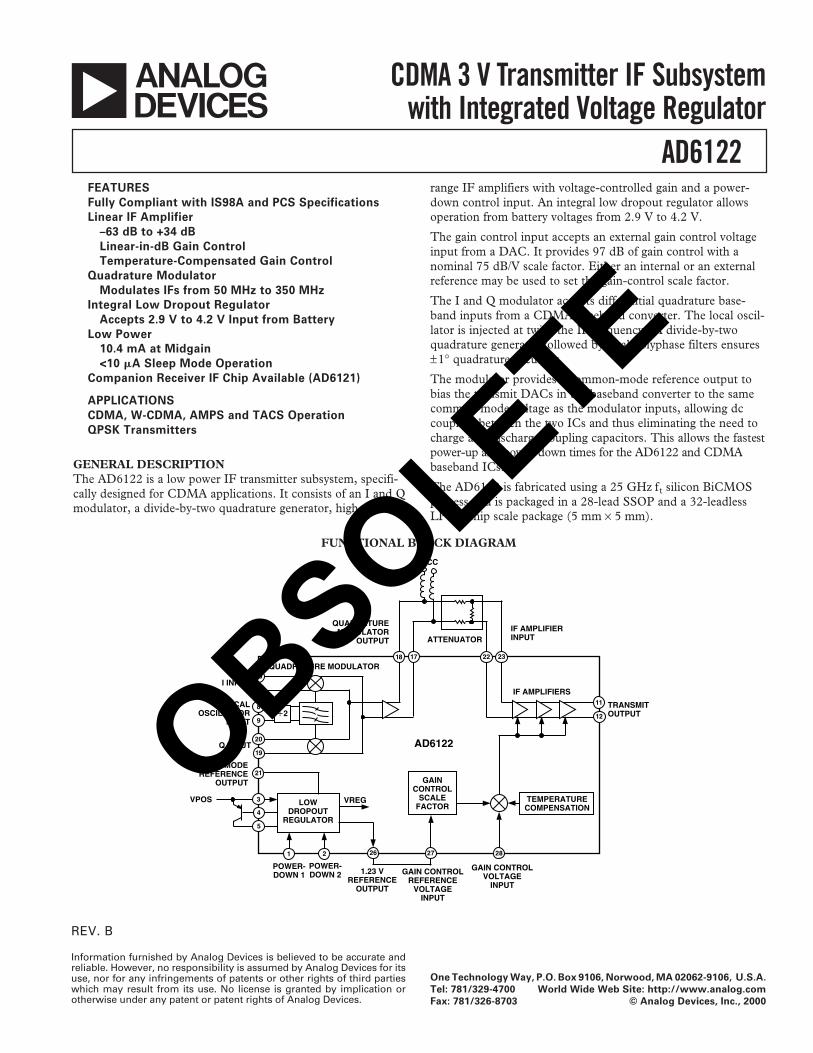
REV. B Information furnished by Analog Devices is believed to be accurate and reliable. However, no responsibility is assumed by Analog Devices for its use, nor for any infringements of patents or other rights of third parties which may result from its use. No license is granted by implication or otherwise under any patent or patent rights of Analog Devices. a AD6122 One Technology Way, P.O. Box 9106, Norwood, MA 02062-9106, U.S.A. Tel: 781/329-4700 World Wide Web Site: http://www.analog.com Fax: 781/326-8703 © Analog Devices, Inc., 2000 CDMA 3 V Transmitter IF Subsystem with Integrated Voltage Regulator FUNCTIONAL BLOCK DIAGRAM I INPUT Q INPUT LOCAL OSCILLATOR INPUT ATTENUATOR LOW DROPOUT REGULATOR COMMON-MODE REFERENCE OUTPUT VREG POWER- DOWN 1 1.23 V REFERENCE OUTPUT VPOS TEMPERATURE COMPENSATION GAIN CONTROL SCALE FACTOR GAIN CONTROL VOLTAGE INPUT GAIN CONTROL REFERENCE VOLTAGE INPUT TRANSMIT OUTPUT IF AMPLIFIERS QUADRATURE MODULATOR POWER- DOWN 2 IF AMPLIFIER INPUT QUADRATURE MODULATOR OUTPUT 2 AD6122 VCC FEATURES Fully Compliant with IS98A and PCS Specifications Linear IF Amplifier –63 dB to +34 dB Linear-in-dB Gain Control Temperature-Compensated Gain Control Quadrature Modulator Modulates IFs from 50 MHz to 350 MHz Integral Low Dropout Regulator Accepts 2.9 V to 4.2 V Input from Battery Low Power 10.4 mA at Midgain <10 A Sleep Mode Operation Companion Receiver IF Chip Available (AD6121) APPLICATIONS CDMA, W-CDMA, AMPS and TACS Operation QPSK Transmitters GENERAL DESCRIPTION The AD6122 is a low power IF transmitter subsystem, specifi- cally designed for CDMA applications. It consists of an I and Q modulator, a divide-by-two quadrature generator, high dynamic range IF amplifiers with voltage-controlled gain and a power- down control input. An integral low dropout regulator allows operation from battery voltages from 2.9 V to 4.2 V. The gain control input accepts an external gain control voltage input from a DAC. It provides 97 dB of gain control with a nominal 75 dB/V scale factor. Either an internal or an external reference may be used to set the gain-control scale factor. The I and Q modulator accepts differential quadrature base- band inputs from a CDMA baseband converter. The local oscil- lator is injected at twice the IF frequency. A divide-by-two quadrature generator followed by dual polyphase filters ensures ± 1° quadrature accuracy. The modulator provides a common-mode reference output to bias the transmit DACs in the baseband converter to the same common-mode voltage as the modulator inputs, allowing dc coupling between the two ICs and thus eliminating the need to charge and discharge coupling capacitors. This allows the fastest power-up and power-down times for the AD6122 and CDMA baseband ICs. The AD6122 is fabricated using a 25 GHz f t silicon BiCMOS process and is packaged in a 28-lead SSOP and a 32-leadless LPCC chip scale package (5 mm × 5 mm). OBSOLETE
Transcript of CDMA 3 V Transmitter IF Subsystem with Integrated Voltage ... · rev. b ad6122 –3– absolute...
REV. B
Information furnished by Analog Devices is believed to be accurate andreliable. However, no responsibility is assumed by Analog Devices for itsuse, nor for any infringements of patents or other rights of third partieswhich may result from its use. No license is granted by implication orotherwise under any patent or patent rights of Analog Devices.
aAD6122
One Technology Way, P.O. Box 9106, Norwood, MA 02062-9106, U.S.A.
Tel: 781/329-4700 World Wide Web Site: http://www.analog.com
Fax: 781/326-8703 © Analog Devices, Inc., 2000
CDMA 3 V Transmitter IF Subsystemwith Integrated Voltage Regulator
FUNCTIONAL BLOCK DIAGRAM
I INPUT
Q INPUT
LOCALOSCILLATOR
INPUT
ATTENUATOR
LOWDROPOUT
REGULATOR
COMMON-MODEREFERENCE
OUTPUT
VREG
POWER-DOWN 1 1.23 V
REFERENCEOUTPUT
VPOS TEMPERATURECOMPENSATION
GAINCONTROL
SCALEFACTOR
GAIN CONTROLVOLTAGE
INPUT
GAIN CONTROLREFERENCE
VOLTAGEINPUT
TRANSMITOUTPUT
IF AMPLIFIERS
QUADRATURE MODULATOR
POWER-DOWN 2
IF AMPLIFIERINPUT
QUADRATUREMODULATOR
OUTPUT
2
AD6122
VCC
FEATURES
Fully Compliant with IS98A and PCS Specifications
Linear IF Amplifier
–63 dB to +34 dB
Linear-in-dB Gain Control
Temperature-Compensated Gain Control
Quadrature Modulator
Modulates IFs from 50 MHz to 350 MHz
Integral Low Dropout Regulator
Accepts 2.9 V to 4.2 V Input from Battery
Low Power
10.4 mA at Midgain
<10 A Sleep Mode Operation
Companion Receiver IF Chip Available (AD6121)
APPLICATIONS
CDMA, W-CDMA, AMPS and TACS Operation
QPSK Transmitters
GENERAL DESCRIPTIONThe AD6122 is a low power IF transmitter subsystem, specifi-cally designed for CDMA applications. It consists of an I and Qmodulator, a divide-by-two quadrature generator, high dynamic
range IF amplifiers with voltage-controlled gain and a power-down control input. An integral low dropout regulator allowsoperation from battery voltages from 2.9 V to 4.2 V.
The gain control input accepts an external gain control voltageinput from a DAC. It provides 97 dB of gain control with anominal 75 dB/V scale factor. Either an internal or an externalreference may be used to set the gain-control scale factor.
The I and Q modulator accepts differential quadrature base-band inputs from a CDMA baseband converter. The local oscil-lator is injected at twice the IF frequency. A divide-by-twoquadrature generator followed by dual polyphase filters ensures±1° quadrature accuracy.
The modulator provides a common-mode reference output tobias the transmit DACs in the baseband converter to the samecommon-mode voltage as the modulator inputs, allowing dccoupling between the two ICs and thus eliminating the need tocharge and discharge coupling capacitors. This allows the fastestpower-up and power-down times for the AD6122 and CDMAbaseband ICs.
The AD6122 is fabricated using a 25 GHz ft silicon BiCMOSprocess and is packaged in a 28-lead SSOP and a 32-leadlessLPCC chip scale package (5 mm × 5 mm).
OBSOLETE
REV. B–2–
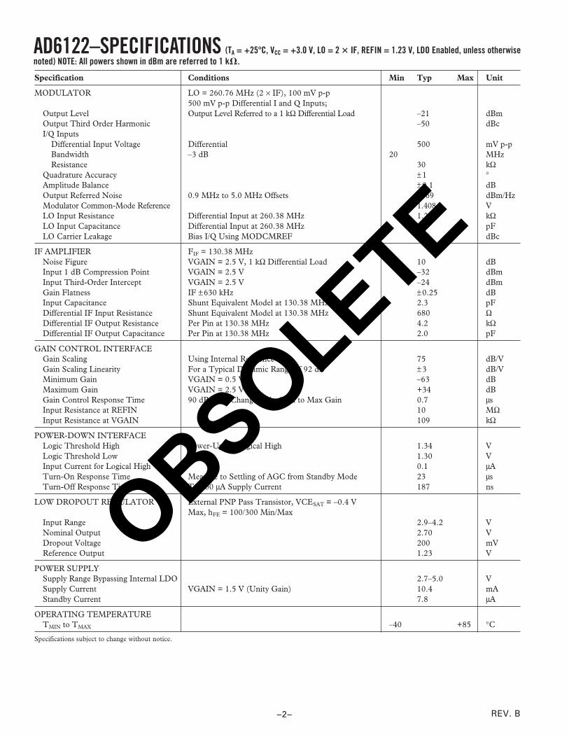
AD6122–SPECIFICATIONS (TA = +25C, VCC = +3.0 V, LO = 2 IF, REFIN = 1.23 V, LDO Enabled, unless otherwisenoted) NOTE: All powers shown in dBm are referred to 1 k.
Specification Conditions Min Typ Max Unit
MODULATOR LO = 260.76 MHz (2 × IF), 100 mV p-p500 mV p-p Differential I and Q Inputs;
Output Level Output Level Referred to a 1 kΩ Differential Load –21 dBmOutput Third Order Harmonic –50 dBcI/Q Inputs
Differential Input Voltage Differential 500 mV p-pBandwidth –3 dB 20 MHzResistance 30 kΩ
Quadrature Accuracy ± 1 °Amplitude Balance ±0.1 dBOutput Referred Noise 0.9 MHz to 5.0 MHz Offsets –169 dBm/HzModulator Common-Mode Reference 1.408 VLO Input Resistance Differential Input at 260.38 MHz 1.2 kΩLO Input Capacitance Differential Input at 260.38 MHz 2.4 pFLO Carrier Leakage Bias I/Q Using MODCMREF –40 dBc
IF AMPLIFIER FIF = 130.38 MHzNoise Figure VGAIN = 2.5 V, 1 kΩ Differential Load 10 dBInput 1 dB Compression Point VGAIN = 2.5 V –32 dBmInput Third-Order Intercept VGAIN = 2.5 V –24 dBmGain Flatness IF ±630 kHz ±0.25 dBInput Capacitance Shunt Equivalent Model at 130.38 MHz 2.3 pFDifferential IF Input Resistance Shunt Equivalent Model at 130.38 MHz 680 ΩDifferential IF Output Resistance Per Pin at 130.38 MHz 4.2 kΩDifferential IF Output Capacitance Per Pin at 130.38 MHz 2.0 pF
GAIN CONTROL INTERFACEGain Scaling Using Internal Reference 75 dB/VGain Scaling Linearity For a Typical Dynamic Range of 92 dB ± 3 dB/VMinimum Gain VGAIN = 0.5 V –63 dBMaximum Gain VGAIN = 2.5 V +34 dBGain Control Response Time 90 dB Gain Change, Min Gain to Max Gain 0.7 µsInput Resistance at REFIN 10 MΩInput Resistance at VGAIN 109 kΩ
POWER-DOWN INTERFACELogic Threshold High Power-Up on Logical High 1.34 VLogic Threshold Low 1.30 VInput Current for Logical High 0.1 µATurn-On Response Time Measure to Settling of AGC from Standby Mode 23 µsTurn-Off Response Time To 200 µA Supply Current 187 ns
LOW DROPOUT REGULATOR External PNP Pass Transistor, VCESAT = –0.4 VMax, hFE = 100/300 Min/Max
Input Range 2.9–4.2 VNominal Output 2.70 VDropout Voltage 200 mVReference Output 1.23 V
POWER SUPPLYSupply Range Bypassing Internal LDO 2.7–5.0 VSupply Current VGAIN = 1.5 V (Unity Gain) 10.4 mAStandby Current 7.8 µA
OPERATING TEMPERATURETMIN to TMAX –40 +85 °C
Specifications subject to change without notice.
OBSOLETE
REV. B
AD6122
–3–
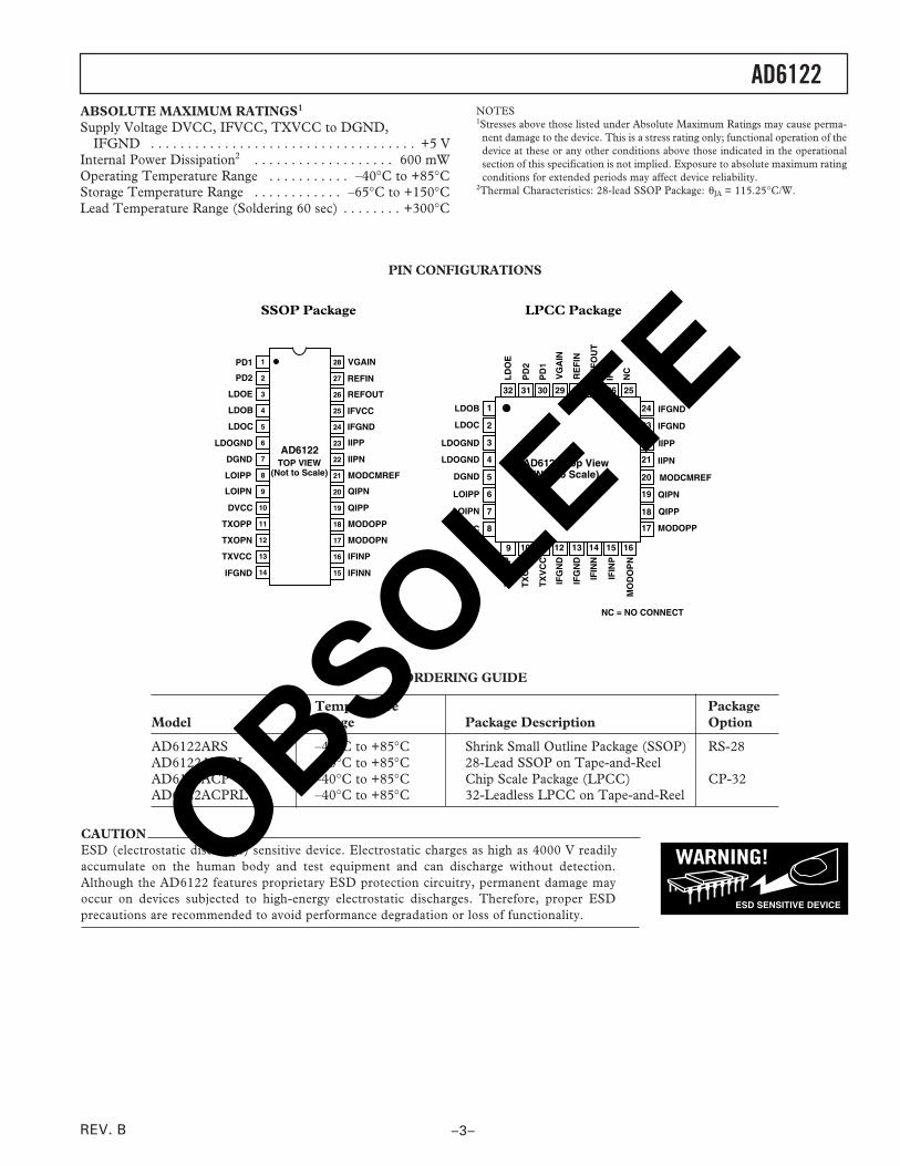
ABSOLUTE MAXIMUM RATINGS1
Supply Voltage DVCC, IFVCC, TXVCC to DGND,IFGND . . . . . . . . . . . . . . . . . . . . . . . . . . . . . . . . . . . . +5 V
Internal Power Dissipation2 . . . . . . . . . . . . . . . . . . . 600 mWOperating Temperature Range . . . . . . . . . . . –40°C to +85°CStorage Temperature Range . . . . . . . . . . . . –65°C to +150°CLead Temperature Range (Soldering 60 sec) . . . . . . . . +300°C
ORDERING GUIDE
Temperature PackageModel Range Package Description Option
AD6122ARS –40°C to +85°C Shrink Small Outline Package (SSOP) RS-28AD6122ARSRL –40°C to +85°C 28-Lead SSOP on Tape-and-ReelAD6122ACP –40°C to +85°C Chip Scale Package (LPCC) CP-32AD6122ACPRL –40°C to +85°C 32-Leadless LPCC on Tape-and-Reel
PIN CONFIGURATIONS
LDOC
PD
1
PD
2
2 23
3 22
4 21
5 20
6 19
7 18
8 17
1 24
10
31
11
30
12
29
13
28
14
27
15
26
16
25
NC
9
32
AD6122 Top View(Not to Scale)
NC = NO CONNECT
LDOB
LDOGND
LDOGND
DGND
LOIPP
LOIPN
DVCC MODOPP
QIPP
QIPN
MODCMREF
IIPN
IIPP
IFGND
IFGND
TX
OP
P
TX
OP
N
TX
VC
C
IFG
ND
IFG
ND
IFIN
N
IFIN
P
MO
DO
PN
IFV
CC
RE
FO
UT
RE
FIN
VG
AIN
LD
OE
LPCC Package
TOP VIEW(Not to Scale)
28
27
26
25
24
23
22
21
20
19
18
17
16
15
1
2
3
4
5
6
7
8
9
10
11
12
13
14
AD6122
IFGND
TXVCC
TXOPN
TXOPP
DVCC
LOIPN
LOIPP
PD1
PD2
LDOE
LDOB
DGND
LDOGND
LDOC
IFINN
IFINP
MODOPN
MODOPP
QIPP
QIPN
MODCMREF
VGAIN
REFIN
REFOUT
IFVCC
IIPN
IIPP
IFGND
SSOP Package
CAUTIONESD (electrostatic discharge) sensitive device. Electrostatic charges as high as 4000 V readilyaccumulate on the human body and test equipment and can discharge without detection.Although the AD6122 features proprietary ESD protection circuitry, permanent damage mayoccur on devices subjected to high-energy electrostatic discharges. Therefore, proper ESDprecautions are recommended to avoid performance degradation or loss of functionality.
WARNING!
ESD SENSITIVE DEVICE
NOTES1Stresses above those listed under Absolute Maximum Ratings may cause perma-
nent damage to the device. This is a stress rating only; functional operation of thedevice at these or any other conditions above those indicated in the operationalsection of this specification is not implied. Exposure to absolute maximum ratingconditions for extended periods may affect device reliability.
2Thermal Characteristics: 28-lead SSOP Package: θJA = 115.25°C/W.
OBSOLETE

REV. B
AD6122
–4–
PIN FUNCTION DESCRIPTIONS
SSOP LPCCPin # Pin # Pin Label Description Function
1 30 PD1 Power-Down 1 IF Amplifier Power-Down Control Input; CMOS Com-patible; HIGH = Entire IC Powers Down, LOW = IFAmplifiers On.
2 31 PD2 Power-Down 2 Modulator Power-Down Control Input; CMOS Compat-ible; HIGH = Modulator Off , LOW = Modulator On.
3 32 LDOE Low Dropout Regulator Pass Connects to Emitter of External PNP Pass TransistorTransistor Emitter Connection and VCC.
4 1 LDOB Low Dropout Regulator Pass Connects to Base of External PNP Pass Transistor.Transistor Base
5 2 LDOC Low Dropout Regulator Pass Connects to Collector of External PNP Pass Transistor.Transistor Collector
6 3, 4 LDOGND Low Dropout Regulator Ground Ground.7 5 DGND Digital Ground Ground.8 6 LOIPP Local Oscillator “Positive” Input Connects to Local Oscillator; AC Coupled.9 7 LOIPN Local Oscillator “Negative” Input Connects to Ground via Decoupling Capacitor.10 8 DVCC Digital VCC Connects to Digital Supply.11 9 TXOPP Transmit Output “Positive” Connects to Output Filter; AC Coupled.12 10 TXOPN Transmit Output “Negative” Connects to Output Filter; AC Coupled.13 11 TXVCC Transmit Output VCC Connects to LDO Output via Decoupling Network.14 12, 13 IFGND IF Ground Ground.15 14 IFINN IF Input “Negative” IF “Negative” Input from LC Roofing Filter.16 15 IFINP IF Input “Positive” IF “Positive” Input from LC Roofing Filter.17 16 MODOPN Modulator “Negative” If Output Output Modulator Output to LC Roofing Filter.18 17 MODOPP Modulator “Positive” Output Modulator Output to LC Roofing Filter.19 18 QIPP Q Input “Positive” Connects to Q “Positive” Output of Baseband IC.20 19 QIPN Q Input “Negative” Connects to Q “Negative” Output of Baseband IC.21 20 MODCMREF Modulator Common-Mode Connects to CDMA Baseband Converter Tx DAC
Reference Out Common-Mode Reference Input.22 21 IIPN I Input “Negative” Connects to I “Negative” Output of Baseband IC.23 22 IIPP I Input “Positive” Connects to I “Positive” Output of Baseband IC.24 23, 24 IFGND Ground Connects to IF Ground.
25 NC No Connect25 26 IFVCC IF VCC Connects to Decoupled Output of LDO Regulator.26 27 REFOUT Gain Control Reference Output Provides 1.23 V Voltage Reference Output for DAC in
CDMA Baseband Converter and REFIN.27 28 REFIN Gain Control Reference Input Accepts 1.23 V Reference Input from REFOUT or
External Reference.28 29 VGAIN Gain Control Voltage Input Accepts Gain Control Input Voltage from External DAC.
Max Gain = 2.5 V; Min Gain = 0.5 V.OBSOLETE

REV. B
AD6122
–5–
Test Figures
2
5
X1 VP
AD830
I DATA–15V
0.1F
MODCMREFA=1
V–1X2
Y1
Y2VN
1
3
4
+15V0.1F
8
7
2
5
X1 VP
AD830
–15V0.1F
MODCMREFA=1
X2
Y1
Y2VN
1
3
4
+15V0.1F
8
7
MUST BE EQUALLENGTHS
2
5
X1 VP
AD830
Q DATA–15V
0.1F
MODCMREFA=1
X2
Y1
Y2VN
1
3
4
+15V0.1F
8
7
2
5
X1 VP
AD830
–15V0.1F
MODCMREFA=1
X2
Y1
Y2VN
1
3
4
+15V0.1F
8
7
MUST BE EQUALLENGTHS
AD6122
IIPP
IIPN
QIPP
QIPN
LOIPP
LO INPUT
MODCMREF
10nF
10nF
0.1F
MOD_OUT
VREG OUT
450
205
450
0.1FVREG OUT
MODOPP
MODOPN
50
50
50
50
50
50
OUT
OUT
OUT
OUT
V–1
V–1
V–1
V–1
V–1
V–1
V–1
LOIPN
Figure 1. Quadrature Modulator’s Characterization Input and Output Impedance MatchesOBSOLETE

REV. B
AD6122
–6–
MOD OUT
I CHANNEL
Q CHANNEL
LO INPUT
IF INRF SOURCE 1
AUX MEASPORT
NOTE: RF CABLES FOR I AND Q PATHS MUST BE OF EQUAL LENGTH
IFTX OUT
I DATA
Q DATA
RF SOURCE 2
R&S FSEA20/30SPECTRUMANALYZERRF
INPUT
R&SSMT03
RF
R&SSMT03
RF
HPE3610POWER SUPPLY
HP34970ADATA ACQUISITION& SWITCH CONTROL
DC MEASUREMENTS& CONTROL BITS
TO RF SWITCHES
TEKTRONIXAFG2002
500mVp-p DIFFERENTIAL
TEST BED MOTHERBOARD
Figure 3. General Test Set
10nF
10nF
0.1F
TOSPECTRUMANALYZER
VREG OUT
453
205
453
0.1FVREG OUT
PULL-UP INDUCTORS CHOSENFOR PEAK RESPONSE AT THETEST FREQUENCY.
10nF
10nF
RF SOURCE
511
383
383
4:1
IFINN
IFINP TXOPP
TXOPN
1:8
AD6122
Figure 2. IF Amplifier’s Characterization Input and Output Impedance Matches
OBSOLETE

REV. B
AD6122
–7–
10nF
10nF
0.1F
VREG OUT
453
205
453
0.1FVREG OUT
PULL-UP INDUCTORS CHOSENFOR PEAK RESPONSE AT THETEST FREQUENCY.
10nF
10nF
NOISESOURCE
REACTIVECONJUGATE
MATCH
TO NOISEFILTERMETER
4:1
IFINN
IFINP TXOPP
TXOPN
1:8
AD6122
Figure 4. IF Amplifier’s Noise Figure Test Set
HP8116AFUNCTION GEN.
4kHz, 0V TO 2.7VSQ. WAVE
ROHDE & SCHWARZSMT03
100kHz, –30dBm
AD6122 TEST BED
PD1,PD2
IFIN
IFOUT
TEKTRONIX TDS 744A
CH 1 WITH X10 PROBE
CH 2 WITH COAX CABLE50
b. Response Time from PD1 and PD2 Control to IF Output
HP8116AFUNCTION GEN.
4 kHz, 0.5V TO 2.5VSQ. WAVE
ROHDE & SCHWARZSMT03
100MHz, –30dBm
AD6122 TEST BED
AGC IFIN
IFOUT
TEKTRONIX TDS 744A
CH 1 WITH X10 PROBE
CH 2 WITH COAX CABLE50
a. Response Time from Gain Control to IF Output
Figure 5. Response Time Setup
OBSOLETE
REV. B
AD6122
–8–
A–40
–140
–130
–120
–110
–100
–90
–80
–70
–60
–50
CL1
1
CU1
REF LEV–40dBm
CENTER 130.38MHz 519kHz/DIV SPAN 5.19MHz
RBWVBWSWT
30kHz100kHz2s UNIT dBm
–49.18dBm130.67458918MHz
–33.92dBm–77.32dB
77.46dB
(T1)1
CH PWRACP UPAVE LOW
PO
WE
R –
dB
m
Figure 6. Spectral Plot at Modulator Outputs: ACPR
FREQUENCY – MHz
–5050 350100
LO
LE
AK
AG
E –
dB
c
150 200 250 300
–45
–35
–40
Figure 7. Modulator LO Leakage vs. Output Frequency
OUTPUT FREQUENCY – MHz
–15
–20
–4050 350100
OU
TP
UT
DE
SIR
ED
SID
EB
AN
D L
EV
EL
–d
Bm
RE
FE
RR
ED
TO
1k
150 200 250 300
–25
–30
–35
Figure 8. Modulator Output Desired Sideband vs.Output Frequency Without Roofing Filter
–Typical Performance Characteristics
OUTPUT FREQUENCY – MHz
–30
–4550 350100
UN
DE
SIR
ED
SID
EB
AN
D –
dB
c
150 200 250 300
–35
–40
Figure 9. Modulator Output Undesired Sideband vs.Output Frequency
MODULATOR, I = Q – dBV
–10
–15
–35–14.0 –2.0–12.0
MO
DU
LA
TO
R O
UT
PU
T –
dB
m R
EF
ER
RE
DT
O A
1k
DIF
FE
RE
NT
IAL
LO
AD
–10.0 –8.0 –6.0 –4.0
–20
–25
–30
Figure 10. Modulator Gain: Input (dBV) vs. Output (dBm)
OUTPUT FREQUENCY – MHz
–6550 350100
TH
IRD
HA
RM
ON
IC –
dB
c
150 200 250 300
–45
–55
–60
–50
Figure 11. Modulator Third Harmonic
OBSOLETE
REV. B
AD6122
–9–
VGAIN – V
40
20
–800.5 2.51.0
GA
IN –
dB
Wit
h a
1k
Lo
ad
1.5 2.0
0
–40
–60
–20
TA = –40C
TA = +85C
TA = +25C
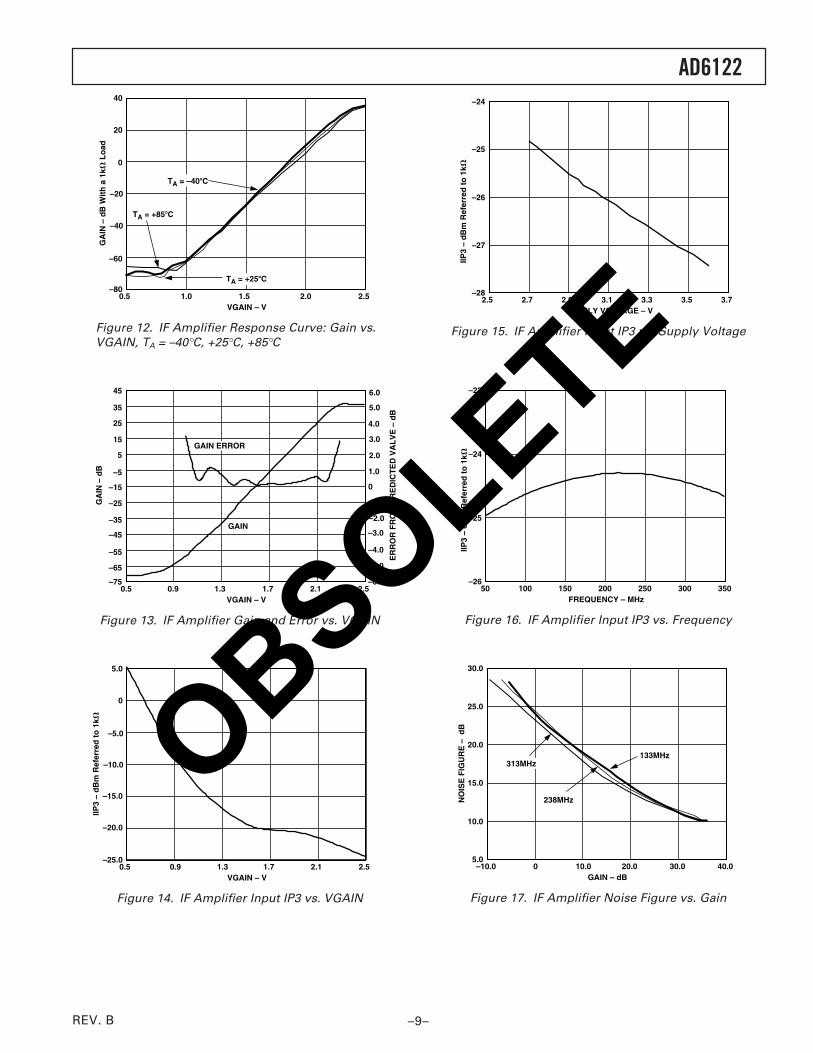
Figure 12. IF Amplifier Response Curve: Gain vs.VGAIN, TA = –40°C, +25°C, +85°C
VGAIN – V
45
25
–750.5 2.50.9
ER
RO
R F
RO
M P
RE
DIC
TE
D V
AL
VE
– d
B
1.3 1.7 2.1
5
–15
–55
–6.0
–5.0
–35
6.0
5.0
3.0
1.0
–1.0 GA
IN –
dB
–65
–45
–25
–5
15
35
4.0
2.0
0
–4.0
–3.0
–2.0GAIN
GAIN ERROR
Figure 13. IF Amplifier Gain and Error vs. VGAIN
VGAIN – V
5.0
0
–25.00.5 2.50.9
IIP3
– d
Bm
Ref
erre
d t
o 1
k
1.3 1.7 2.1
–5.0
–15.0
–20.0
–10.0
Figure 14. IF Amplifier Input IP3 vs. VGAIN
SUPPLY VOLTAGE – V
–24
–25
–282.5 3.72.7
IIP3
– d
Bm
Ref
erre
d t
o 1
k
2.9 3.1 3.3 3.5
–26
–27
Figure 15. IF Amplifier Input IP3 vs. Supply Voltage
–23
–2650 350100
IIP3
– d
Bm
Ref
erre
d t
o 1
k
150 200 250 300
–24
–25
FREQUENCY – MHz
Figure 16. IF Amplifier Input IP3 vs. Frequency
GAIN – dB
30.0
25.0
5.0–10.0 40.00
NO
ISE
FIG
UR
E –
dB
10.0 20.0 30.0
20.0
15.0
10.0
238MHz
313MHz133MHz
Figure 17. IF Amplifier Noise Figure vs. Gain
OBSOLETE
REV. B
AD6122
–10–
FREQUENCY – MHz
40
20
–8050 350100
GA
IN –
dB
150 200 250 300
0
–20
–60
–40
VGAIN = 2.5V
VGAIN = 2.0V
VGAIN = 1.5V
VGAIN = 1.0V
VGAIN = 0.5V
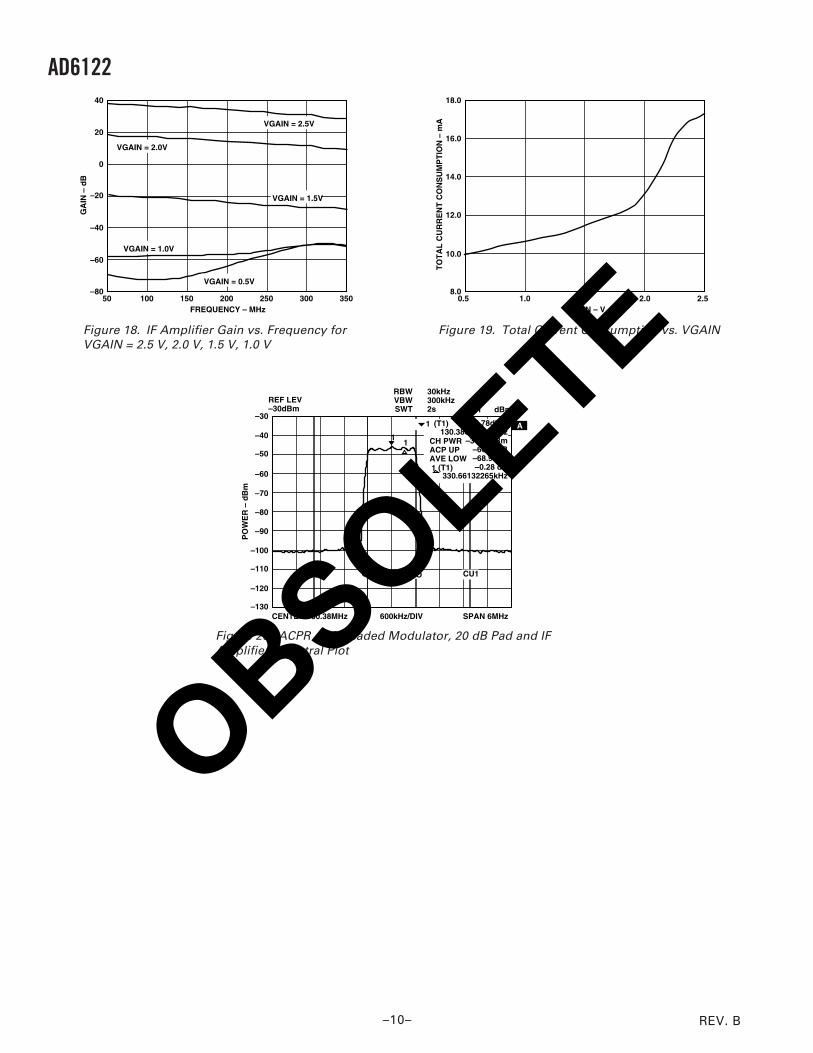
Figure 18. IF Amplifier Gain vs. Frequency forVGAIN = 2.5 V, 2.0 V, 1.5 V, 1.0 V
A–40
–130
–120
–110
–100
–90
–80
–70
–60
–50
CL1
1
CU1COCO
–46.78dBm130.38000000MHz
–31.93dBm–66.95dB–68.95dB–0.28 dB
330.66132265kHz
(T1)1
CH PWRACP UPAVE LOW
REF LEV–30dBm
CENTER 130.38MHz 600kHz/DIV SPAN 6MHz
RBWVBWSWT
30kHz300kHz2s UNIT dBm
–30
1 (T1)
1
PO
WE
R –
dB
m
Figure 20. ACPR of Cascaded Modulator, 20 dB Pad and IFAmplifier: Spectral Plot
VGAIN – V
18.0
16.0
8.00.5 2.5
TO
TA
L C
UR
RE
NT
CO
NS
UM
PT
ION
– m
A
1.0 1.5 2.0
14.0
12.0
10.0
Figure 19. Total Current Consumption vs. VGAIN
OBSOLETE

REV. B
AD6122
–11–
THEORY OF OPERATIONThe CDMA Transmitter IF Subsystem (Figure 21) consists ofan I and Q modulator with a divide-by-two quadrature genera-tor, high dynamic range IF amplifiers with voltage-controlledgain, a low dropout regulator and power-down control inputs.
I and Q ModulatorThe I and Q modulator accepts differential quadrature basebandinputs from CDMA baseband converters. The LO is injected attwice the IF frequency. A divide-by-two quadrature generatorfollowed by dual polyphase filters ensures ±1° quadrature accu-racy (Figure 22).
For 500 mV p-p differential I and Q input signals, the outputpower of the modulator will be –21 dBm referred to 1 kΩ whenthe output of the modulator is loaded with a 1 kΩ differentialload. With the maximum input conditions stated above, themodulator outputs are a 225 µA p-p differential current; conse-quently, the output load will greatly affect the output power ofthe modulator.
2180
2
POLYPHASEFILTERS
I
Q
I
Q
2 IFLO INPUT
QUADRATUREOUTPUT TOMODULATOR
Figure 22. Simplified Quadrature Generator Circuit
The I and Q modulator also provides a common mode referencesignal at the MODCMREF pin. This voltage is a dc voltage setto 1.408 V when a 2.7 V supply is used. It is used to dc biasthe output of the DAC that provides I and Q inputs to themodulator.
IF Amplifiers and Gain ControlThe IF amplifiers provide an 86 dB linear in dB gain controlrange. The input stage uses a differential, continuously variableattenuator based on Analog Devices’ patented X-AMP™ topol-ogy. This low noise attenuator consists of a differential R-2Rladder network, linear interpolator and a fixed gain amplifier.The IF amplifier’s input impedance is 1 kΩ differential. Similarto the I and Q modulator’s output, the IF amplifier’s output is adifferential current, which will vary depending upon the gaincontrol voltage. In order to achieve the specified gain, the out-put of the IF amplifiers should be loaded with a 1 kΩ differen-tial load.
The gain control circuits contain both temperature compensa-tion circuitry and a choice of internal or external reference foradjusting the gain scale factor. The gain control input acceptsan external gain control voltage input from a DAC. It provides97 dB of gain control range with a nominal 75 dB/V scale factor.
The external gain control input signal should be a clean signal.It is recommended to filter this signal in order to eliminate thenoise that results from the DAC. If a noisy signal is used for thegain control voltage, VGAIN inband and adjacent channel noisepeaking can occur at the output of the AD6122. A simple RCfilter can be employed, but care should be taken with its design.If too big a resistor is used, a large voltage drop may occuracross the resistor, resulting in lower gain than expected (as aresult of a lower voltage reaching the AD6122). An RC filterwith a 20 kHz bandwidth, employing a 1 kΩ resistor is appropri-ate. This results in an 8.2 nF capacitor. The resulting circuitis shown in Figure 23. Note that the input resistance at theVGAIN pin is approximately 100 kΩ.
FROMBASEBAND
CONVERTER
AD6122VGAIN
1k
8.2nF 109k
Figure 23. Gain Voltage Filtering
I INPUT
Q INPUT
LOCALOSCILLATOR
INPUT
ATTENUATOR
COMMON-MODEREFERENCE
OUTPUT
VREG
POWER-DOWN 1 1.23 V
REFERENCEOUTPUT
VPOSTEMPERATURE
COMPENSATION
GAIN CONTROLVOLTAGE
INPUTGAIN CONTROL
REFERENCEVOLTAGE
INPUT
TRANSMITOUTPUT
IF AMPLIFIERS
QUADRATURE MODULATOR
VCC
POWER-DOWN 2
IF AMPLIFIERINPUT
QUADRATUREMODULATOR
OUTPUT
2
AD6122
GAINCONTROL
SCALEFACTORLOW
DROPOUTREGULATOR
Figure 21. Block Diagram
X-AMP is a trademark of Analog Devices, Inc.
OBSOLETE

REV. B
AD6122
–12–
The AD6122’s overall gain, expressed in decibels, is linear indB with respect to the automatic gain control (AGC) voltage,VGAIN. Either REFOUT or an external reference voltage con-nected to REFIN may be used to set the voltage range for VGAIN.When the internal 1.23 V reference, REFOUT, is connected toREFIN , VGAIN will control the entire AGC range when it istypically set between 0.5 V and 2.5 V. Minimum gain occurs atminimum voltage on VGAIN and maximum gain occurs at maxi-mum voltage on VGAIN. The maximum and minimum gainwill not change with a change in voltage at REFIN. Rather, theslope of the gain curve will change as a result of a change in therequired range for VGAIN. Figure 24 shows the piecewise linearapproximation of the gain curve for the AD6122.
MINIMUMGAIN
MAXIMUMGAIN
GA
IN –
V/V
VGAIN – V
Figure 24. Piecewise Linear Approximation for theAD6122 Gain Curve
Because the minimum and maximum gain from the AD6122are constant, we can approximate the VGAIN range for agiven REFIN voltage by using Equation 1.
VGAIN
GAIN MinGain REFINMaxGain MinGain
REFIN=×
+( – ) .
–.
1 60 4 (1)
Where MaxGain is the maximum gain (+34 dB) in dB, MinGainis the minimum gain (–63 dB) in dB, REFIN is the referenceinput voltage, in volts, VGAIN is the gain control voltage input,in volts, and GAIN is the particular gain, in dB, we would havefor a given REFIN and VGAIN. Consequently, for any REFINwe choose, we can calculate the VGAIN range by solvingEquation 1 for VGAIN. For example, in order to determine theVGAIN value for the maximum gain condition, given a 1.23 VREFIN, we can solve Equation 1 for VGAIN by substituting+34 dB for GAIN and MaxGain, –63 dB for MinGain and 1.23 Vfor REFIN. VGAIN can then be calculated to be 2.46 V, orapproximately 2.5 V. For the minimum gain condition, we candetermine the VGAIN value by substituting 34 dB for MaxGain,–63 dB for GAIN and MinGain and 1.23 V for REFIN. VGAINcan then be calculated to be 0.492 V or approximately 0.5 V.
Power-Down ControlThe AD6122 can be operated with the IF amplifiers and quadra-ture modulator both powered up, both powered down or withthe IF amplifiers powered up and the modulator powered down.The AD6122 cannot operate with only the modulator powered
up. The control is provided via two control pins, PD1 and PD2.Table I shows the operating modes of the AD6122.
Table I. Operating Modes
PD1 PD2 IF Amp Modulator
0 0 ON ON0 1 ON OFF1 0 INVALID STATE INVALID STATE1 1 OFF OFF
Low Dropout RegulatorThe AD6122 incorporates an integrated low dropout regulator.The regulator accepts inputs from 2.9 V to 4.2 V and supplies aconstant 2.7 V reference output at LDOC. The 2.7 V signal canbe used to provide the dc voltages required for the DVCC,TXVCC and IFVCC dc supplies. In order to configure the lowdropout regulator, an external pass transistor is required. A pnpbipolar junction transistor with a minimum hFE of 100 and amaximum hFE of 300 and a VCESAT of –0.4 V is required. Inorder to use the low dropout regulator, configure the transistor asshown in Figure 25. The 18 pF capacitor in Figure 25 is used fordecoupling the 2.7 V dc signal.
In addition to the low dropout regulator, a band-gap voltagereference produces a 1.23 V reference voltage at REFOUT.This reference voltage will be present whenever a 2.7 V dc sig-nal is present on pin LDOC. This 1.23 V reference voltage canthen be used to provide the gain reference signal required forREFIN and the reference voltage for the transmit DACs in abaseband converter.
AD6122
LDOE
LDOC
LDOB
18pF
2.9V – 4.2V
2.7V
REFOUT 1.23V
PASSTRANSISTOR
Figure 25. Configuring the Low Dropout Regulator
It is possible to bypass the low dropout regulator on the AD6122and use an external regulator instead. In order to bypass theintegrated low dropout regulator, connect pins LDOE, LDOBand LDOC together and then connect them all to the 2.7 Vexternal regulator voltage. This configuration is shown inFigure 26. Even when the low dropout regulator is bypassed,the 1.23 V reference voltage at pin REFOUT is still present.
OBSOLETE

REV. B
AD6122
–13–
FROM EXTERNALVOLTAGE REGULATOR
AD6122
LDOE
LDOC
LDOB
REFOUT 1.23V
Figure 26. Configuration for Bypassing the Low DropoutRegulator
ROOFING FILTERBecause the outputs of the AD6122 modulator are open collec-tor, the parasitic capacitances seen at the output of the modula-tor, and inputs of the IF amplifiers, are high enough to create alow-pass filter, which may attenuate the IF signal. Consequently,the parasitic capacitance must be cancelled by using externalinductors to form a parallel resonant circuit. The external in-ductors and the internal parasitic capacitors form what is knownas the roofing filter, with the resonant frequency given byEquation 2.
f
LCPAR
01
2=
π (2)
where f0 is the IF frequency, in Hertz, CPAR is the total parasiticcapacitance in Farads, and L is the value of external inductors,in henrys.
The roofing filter may be composed of the pull-up inductorsrequired on the open collector outputs of the I and Q modula-tor. This configuration is shown in Figure 27. The 10 nF ca-pacitors are used for ac coupling.
AD6122
MODOPP
MODOPN
IFINP
IFINN
L/2
2CPAR
2CPAR
ATTENUATOR
10nF
L/2 10nF
PARALLELRESONANTCIRCUIT
10nF
VCC
Figure 27. Roofing Filter Configuration
The attenuator is discussed in the next section entitled Measur-ing Adjacent Channel Protection Ratio (ACPR).
In order to confirm whether the roofing filter has been correctlydesigned, sweep the LO frequency and view the output of the IFamplifier on a spectrum analyzer. The signal should peak at theIF frequency if the inductor value is correct. The Q of the filtershould be low enough so that variations in the parasitic capaci-tances should be negligible.
The value of inductor required will be a function of the IF fre-quency at which we are operating. The values of inductors usedduring characterization at Analog Devices are shown in TableII. Because the exact value will also be a function of printedcircuit board layout, we will have to vary the value from those inTable II to those required for our board.
Table II. Roofing Filter Inductor Values
Value of Roofing FilterIF Frequency (MHz) Inductor (nH)
50–125 470126–200 150201–275 68276–350 27
It should be noted that the roofing filter is only required whencascading the output from the I/Q modulator to the input of theIF amplifiers. If we are driving into the IF amplifiers directly, noroofing filter is required, however, pull-up inductors are requiredin order to set the dc voltage of the open collector modulatoroutputs.
MEASURING ADJACENT CHANNEL POWER RATIO(ACPR)At maximum IF gain and specified input conditions (500 mVp-p baseband inputs), the output of the I/Q modulator is 11 dBgreater than the P1 dB (one dB compression point) of the IFamplifiers. This configuration maximizes the ratio of signal toLO feedthrough and also maximizes the signal to noise ratio.Once these ratios are maximized, we can attenuate the noise,signal and LO feedthrough without affecting the ratios. There-fore, attenuation is required between the I/Q modulator and theIF amplifiers.
In order to determine exactly how much attenuation is required,we must recognize that ACPR is a function of the attenuationfrom the modulator outputs to the IF amplifier inputs. As aresult, in order to determine how much attenuation is required,we must first know how good an ACPR performance is desired.If too much attenuation is applied, the ACPR will be very good,but, the IF amplifier’s output power level will be low, possiblyresulting in poor signal to noise ratio and possibly requiringadditional amplification external to the AD6122.
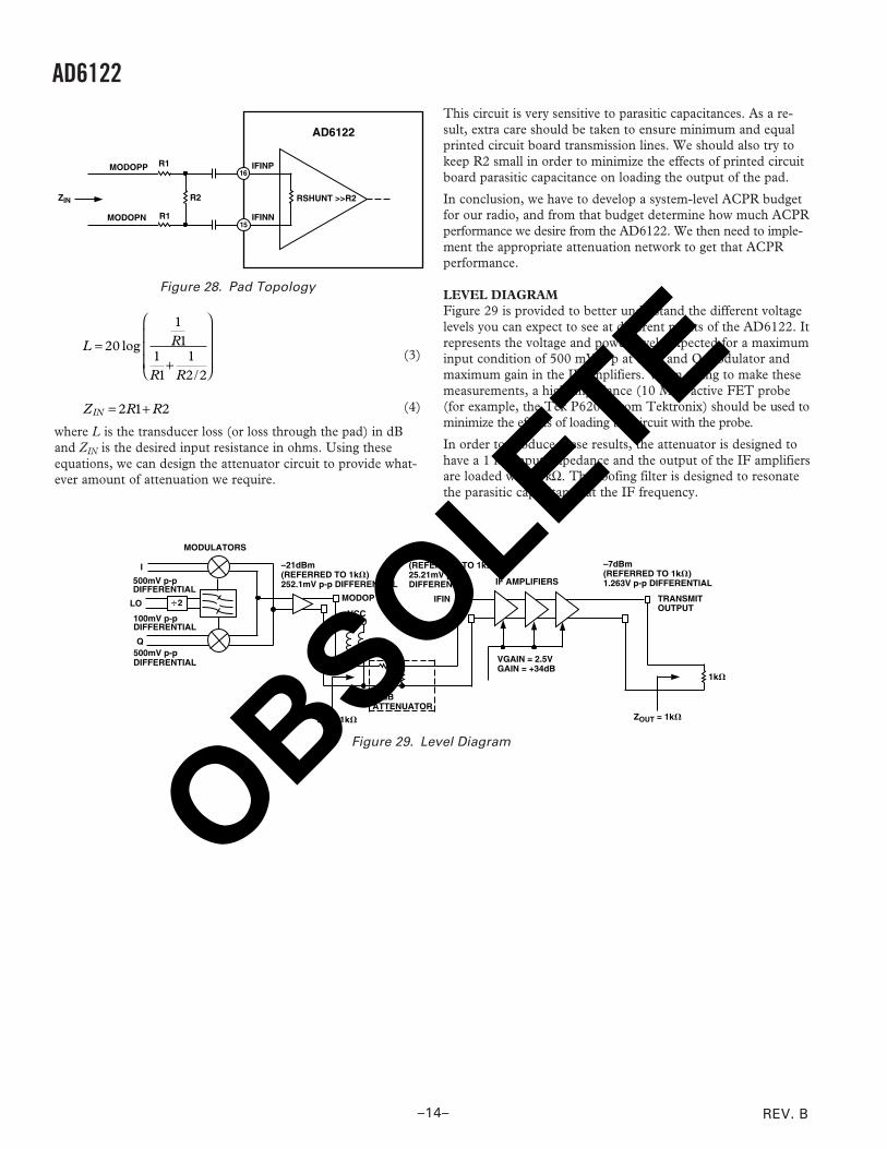
An appropriate method that can be used to provide the correctamount of attenuation between the modulator outputs and theIF amplifier inputs is a simple differential voltage divider. Thetopology and its design equations are shown in Figure 28 andEquations 3 and 4. The input impedance of the IF amplifiers istypically 1 kΩ. As a result, if we design resistor R2 to be muchless than 1 kΩ, we can neglect the effects of the IF amplifier’sinput impedance on the attenuator.
OBSOLETE
REV. B
AD6122
–14–
R2
R1
MODOPP
MODOPN
IFINP
IFINN
ZIN
R1
RSHUNT >>R2
AD6122
Figure 28. Pad Topology
L R
R R
=+
20
11
11
12 2
log
/
(3)
Z R RIN = +2 1 2 (4)
where L is the transducer loss (or loss through the pad) in dBand ZIN is the desired input resistance in ohms. Using theseequations, we can design the attenuator circuit to provide what-ever amount of attenuation we require.
I
Q
LO
MODULATORS
500mV p-pDIFFERENTIAL
500mV p-pDIFFERENTIAL
100mV p-pDIFFERENTIAL
20dBATTENUATOR
VGAIN = 2.5VGAIN = +34dB
TRANSMITOUTPUT
IF AMPLIFIERS
–21dBm(REFERRED TO 1k)252.1mV p-p DIFFERENTIAL
–41dBm(REFERRED TO 1k)25.21mV p-pDIFFERENTIAL
–7dBm(REFERRED TO 1k)1.263V p-p DIFFERENTIAL
MODOP IFIN
ZOUT = 1k
1k
2
ZIN = 1k
VCC
Figure 29. Level Diagram
This circuit is very sensitive to parasitic capacitances. As a re-sult, extra care should be taken to ensure minimum and equalprinted circuit board transmission lines. We should also try tokeep R2 small in order to minimize the effects of printed circuitboard parasitic capacitance on loading the output of the pad.
In conclusion, we have to develop a system-level ACPR budgetfor our radio, and from that budget determine how much ACPRperformance we desire from the AD6122. We then need to imple-ment the appropriate attenuation network to get that ACPRperformance.
LEVEL DIAGRAMFigure 29 is provided to better understand the different voltagelevels you can expect to see at different points of the AD6122. Itrepresents the voltage and power levels expected for a maximuminput condition of 500 mV p-p at the I and Q modulator andmaximum gain in the IF amplifiers. When trying to make thesemeasurements, a high impedance (10 MΩ) active FET probe(for example, the Tek P6204, from Tektronix) should be used tominimize the effects of loading the circuit with the probe.
In order to produce these results, the attenuator is designed tohave a 1 kΩ input impedance and the output of the IF amplifiersare loaded with 1 kΩ. The roofing filter is designed to resonatethe parasitic capacitance at the IF frequency.
OBSOLETE

REV. B
AD6122
–15–
INPUT INTERFACESThe AD6122 interfaces to CDMA baseband converters provid-ing either IF or baseband outputs. The baseband input is pro-vided by direct connection of the baseband converter’s basebandoutput to the baseband input of the AD6122 (Figure 30). TheIF amplifier’s gain control is provided by connection of thetransmit AGC DAC’s output on the baseband converter, through alow-pass filter to the VGAIN pin on the AD6122.
GAINCONTROL
SCALEFACTOR
LOWDROPOUT
REGULATOR
VCC
TEMPERATURECOMPENSATION
TXVCC
IFINN
PD1
2
AD6122
PD2
IFINP
TX AGC DAC
CDMABASEBAND
IC
EXT REF IN
I OUTPUT
I OUTPUT
VCM REF IN
Q OUTPUT
Q OUTPUT
IFVCC
IFGND
IIPP
IIPN
QIPN
QIPP
MODCMREF
MODOPN
MODOPP
REFOUT
REFIN
VGAIN
I
Q
TXOPN
TXOPP
IFGND
DVCC
LOIPN
LOIPP
DGND
LDOGND
LDOC
LDOB
LDOE
VCCVCC
Figure 30. Typical Connections to Baseband IC Using I and Q Inputs with SSOP PackageOBSOLETE
REV. B
AD6122
–16–
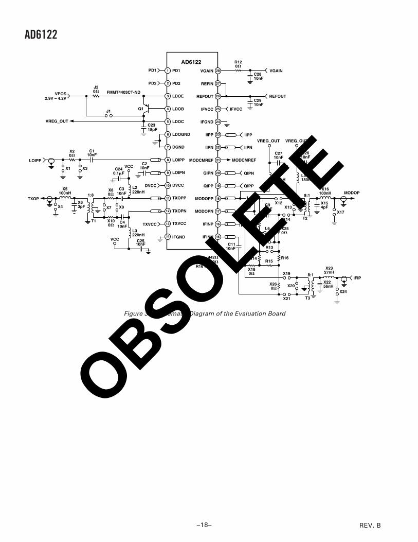
AD6122 Evaluation BoardThe AD6122 Evaluation Board consists of an AD6122, I/O con-nectors, a 20-pin dual header, 2-pin headers and four AD830high speed video difference amplifiers. It allows the user toevaluate the AD6122’s IF amplifier and modulator together orseparately. Because the AD6122 may be used at any IF from 50MHz to 350 MHz, pads are provided on the LOIPP input,TXOP output, MODOP output and IFIP inputs to allow theuser to add matching networks. The board is configured for anIF frequency of 130.38 MHz when shipped. There is no differ-ence between the configuration of the boards with the SSOP orLPCC package.
The AD830s are used to provide single-ended to differentialconversion and the appropriate phase shift for the I and Q datainput pins. As a result, a single-ended signal generator can beused to generate these signals.
In order to test the power-down modes of the AD6122, locatethe two pin headers on the AD6122 evaluation boards labeledPD1 and PD2. By open-circuiting the pins labeled PD1, the IFamplifiers power down. By open-circuiting the pins labeledPD2, the modulator powers down. Note that the IF amplifiersand modulator are powered down unless the pins on the two pinheaders, PD1 and PD2, are short circuited.
The IF input port impedance match used during characteriza-tion of the AD6122 at Analog Devices is as follows:
IFINP
IFINN
AD6122
SIGNALGENERATOR
511
383
383
50
1k
1:8
Figure 31. IF Input Port Impedance Match Used DuringCharacterization at ADI
This is a broadband lossy match used for characterization overthe 50 MHz to 350 MHz frequency range. All dBm referencesin the characterization data collected using this match are refer-enced to 1 kΩ. Note that the 1:8 ratio in Figure 31 is an imped-ance ratio and not a voltage ratio.
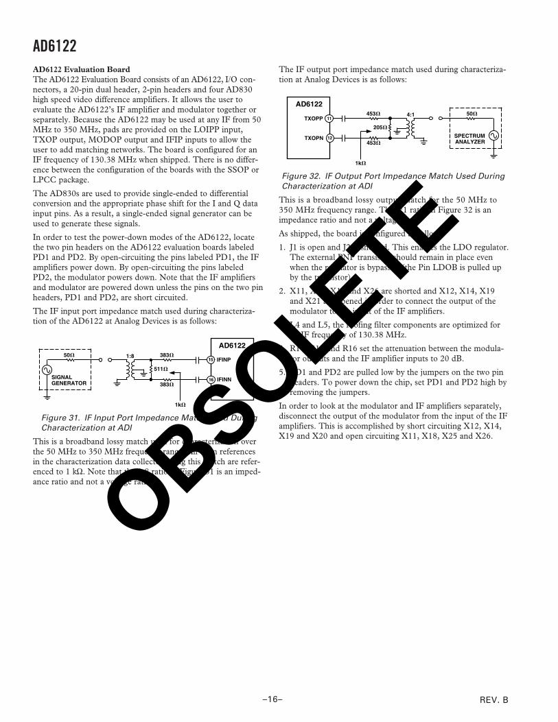
The IF output port impedance match used during characteriza-tion at Analog Devices is as follows:
TXOPP
AD6122
SPECTRUMANALYZER
205
453
453
50
1k
4:1
TXOPN
Figure 32. IF Output Port Impedance Match Used DuringCharacterization at ADI
This is a broadband lossy output match for the 50 MHz to350 MHz frequency range. The 4:1 ratio in Figure 32 is animpedance ratio and not a voltage ratio.
As shipped, the board is configured as follows:
1. J1 is open and J2 is shorted. This enables the LDO regulator.The external PNP transistor should remain in place evenwhen the regulator is bypassed (the Pin LDOB is pulled upby the transistor).
2. X11, X25, X18 and X26 are shorted and X12, X14, X19and X21 are opened in order to connect the output of themodulator to the input of the IF amplifiers.
3. L4 and L5, the roofing filter components are optimized foran IF frequency of 130.38 MHz.
4. R14, R15 and R16 set the attenuation between the modula-tor outputs and the IF amplifier inputs to 20 dB.
5. PD1 and PD2 are pulled low by the jumpers on the two pinheaders. To power down the chip, set PD1 and PD2 high byremoving the jumpers.
In order to look at the modulator and IF amplifiers separately,disconnect the output of the modulator from the input of the IFamplifiers. This is accomplished by short circuiting X12, X14,X19 and X20 and open circuiting X11, X18, X25 and X26.
OBSOLETE
REV. B
AD6122
–17–
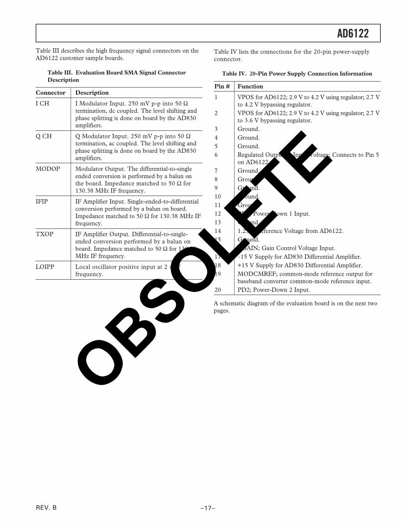
Table III describes the high frequency signal connectors on theAD6122 customer sample boards.
Table III. Evaluation Board SMA Signal ConnectorDescription
Connector Description
I CH I Modulator Input. 250 mV p-p into 50 Ωtermination, dc coupled. The level shifting andphase splitting is done on board by the AD830amplifiers.
Q CH Q Modulator Input. 250 mV p-p into 50 Ωtermination, ac coupled. The level shifting andphase splitting is done on board by the AD830amplifiers.
MODOP Modulator Output. The differential-to-singleended conversion is performed by a balun onthe board. Impedance matched to 50 Ω for130.38 MHz IF frequency.
IFIP IF Amplifier Input. Single-ended-to-differentialconversion performed by a balun on board.Impedance matched to 50 Ω for 130.38 MHz IFfrequency.
TXOP IF Amplifier Output. Differential-to-single-ended conversion performed by a balun onboard. Impedance matched to 50 Ω for 130.38MHz IF frequency.
LOIPP Local oscillator positive input at 2 × IFfrequency.
Table IV lists the connections for the 20-pin power-supplyconnector.
Table IV. 20-Pin Power Supply Connection Information
Pin # Function
1 VPOS for AD6122; 2.9 V to 4.2 V using regulator; 2.7 Vto 4.2 V bypassing regulator.
2 VPOS for AD6122; 2.9 V to 4.2 V using regulator; 2.7 Vto 3.6 V bypassing regulator.
3 Ground.4 Ground.5 Ground.6 Regulated Output or Input Voltage; Connects to Pin 5
on AD6122.7 Ground.8 Ground.9 Ground.10 Ground.11 Ground.12 PD1; Power-Down 1 Input.13 Ground.14 1.23 V Reference Voltage from AD6122.15 Ground.16 VGAIN; Gain Control Voltage Input.17 –15 V Supply for AD830 Differential Amplifier.18 +15 V Supply for AD830 Differential Amplifier.19 MODCMREF; common-mode reference output for
baseband converter common-mode reference input.20 PD2; Power-Down 2 Input.
A schematic diagram of the evaluation board is on the next twopages.
OBSOLETE
REV. B
AD6122
–18–
VREG OUT
FMMT4403CT-NDVPOS2.9V – 4.2V
LOIPP
X1
L2220nH
X63pF
X5100nH 1:8
T1
TXOP
DVCC
X4
L3220nH
C2510nF
VCC
TXVCC
C1010nF
C910nF
X12X13
X14
C30
L6X110 X25
0
C810nF
QIPP
L4180nH
L5180nH
8:1
X17
X154pF
T2
X16100nH MODOP
X80
C310nF
X100
X7 X9
C410nF
VGAIN
REFOUT
IFVCC
VREG OUT
C240.1F
X3
C110nF
X20
C210nF
C2318pF
PD1
PD2
J1
J20
C1110nF R13
R16R15
R14
X19
X20
X21
X180
X260
IIPP
IIPN
QIPN
MODCMREF
C2910nF
IFIP
R14 = 442R15 = 100R16 = 442
C2710nF
C2610nF
VREG OUT
R120
X24
X2327nH
T3
X2256nH
VCC
C2810nF
AD6122PD1
PD2
LDOE
LDOB
LDOC
LDOGND
DGND
LOIPP
LOIPN
DVCC
TXOPP
TXOPN
TXVCC
IFGND
MODCMREF
IIPN
IIPP
IFGND
IFVCC
REFOUT
REFIN
VGAIN
QIPN
QIPP
MODOPP
MODOPN
IFINP
IFINN
Q1
8:1
Figure 33. Schematic Diagram of the Evaluation Board
OBSOLETE
REV. B
AD6122
–19–
2
5AD830
ICH C160.1F
MODCMREFA=1
V–1
1
3
4
8
7
2
5AD830
A=1
1
3
4
+15V
C170.1F
8
7
TOIIPP
R750
R650
MODCMREF
C180.1F
TOIIPN
U2
U3
C150.1F
+15V
R850
–15V
–15V
SOIC PACKAGE
V–1
V–1
V–1
P1
3
7
11
15
19
1
5
9
13
17
L1470nH
REFOUT
VGAIN
FROM VPOS2.9V–4.2V
VREG OUT
+15V
PD2
P2
4
8
12
16
20
2
6
10
14
18–15V
MODCMREF
R410k
R510k
PD1 PD2
VPOS
PD1
C618pF
R110
C130.01F
C518pF
R210
C120.01F
C718pF
R310
C140.01F
TODVCC
TOIFVCC
TOTXVCC VREG OUT
2
5AD830
QCH C200.1F
MODCMREFA=1
1
3
4
8
7
2
5AD830
A=1
1
3
4
+15V
C210.1F
8
7
TOQIPP
R1050
R950
MODCMREF
C220.1F
TOQIPN
U4
U5
C190.1F
+15V
R1150
–15V
–15V
SOIC PACKAGE
V–1
V–1
V–1
V–1
NOTES:1. TO USE THE LDO REGULATOR, SHORT J2 AND OPEN J1.2. TO BYPASS THE REGULATOR, SHORT J1 AND OPEN J23. TO CONNECT THE OUTPUT OF THE MODULATOR TO THE INPUT OF THE IF AMP, SHORT J5 AND J6. TO TEST THE MODULATOR AND THE IF AMP SEPARATELY, OPEN J5 AND J6.4. INDICATES A 50 TRACE.
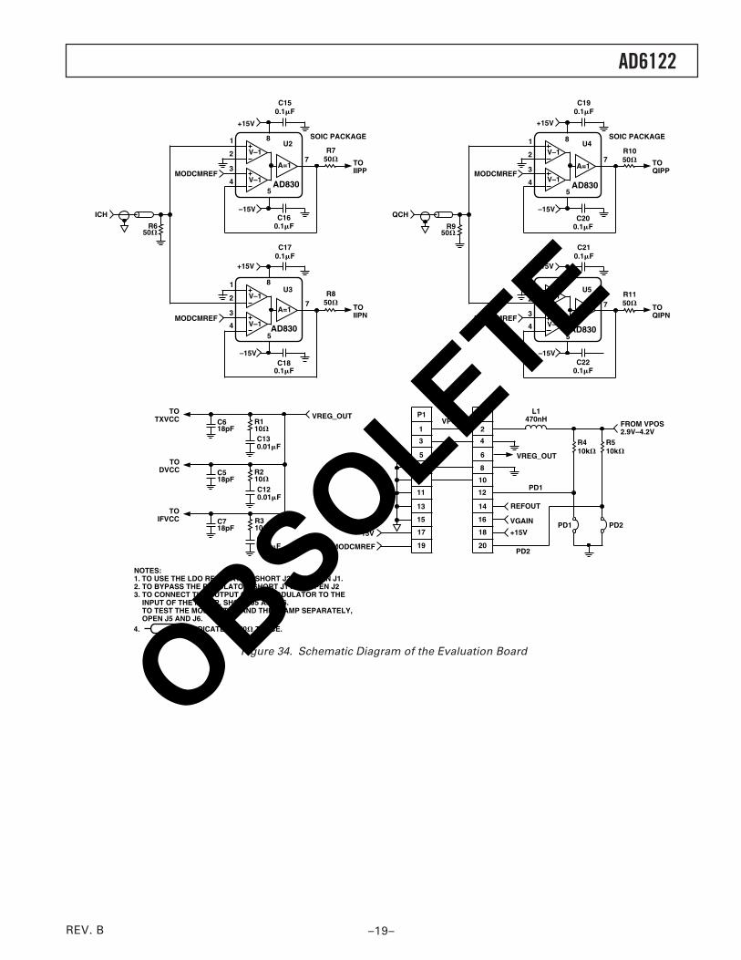
Figure 34. Schematic Diagram of the Evaluation BoardOBSOLETE
REV. B–20–
C00
946a
–.5–
6/00
(re
v. B
)P
RIN
TE
D IN
U.S
.A.
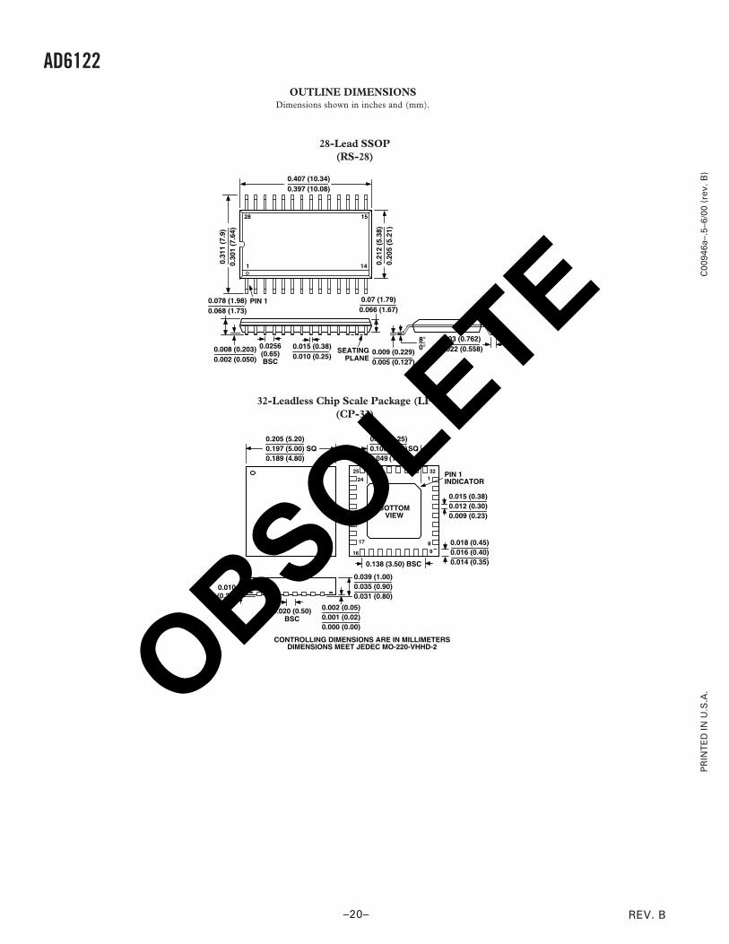
AD6122OUTLINE DIMENSIONS
Dimensions shown in inches and (mm).
28-Lead SSOP(RS-28)
28 15
141
0.407 (10.34)0.397 (10.08)
0.31
1 (7
.9)
0.30
1 (7
.64)
0.21
2 (5
.38)
0.20
5 (5
.21)
PIN 1
SEATINGPLANE
0.008 (0.203)0.002 (0.050)
0.07 (1.79)0.066 (1.67)
0.0256(0.65)BSC
0.078 (1.98)0.068 (1.73)
0.015 (0.38)0.010 (0.25)
0.009 (0.229)0.005 (0.127)
0.03 (0.762)0.022 (0.558)
8°0°
32-Leadless Chip Scale Package (LPCC)(CP-32)
132
9817
BOTTOMVIEW
25
24
16
0.018 (0.45)0.016 (0.40)0.014 (0.35)0.138 (3.50) BSC
PIN 1INDICATOR
0.015 (0.38)0.012 (0.30)0.009 (0.23)
0.128 (3.25)0.106 (2.70) SQ0.049 (1.25)
0.020 (0.50)BSC
0.039 (1.00)0.035 (0.90)0.031 (0.80)
0.002 (0.05)0.001 (0.02)0.000 (0.00)
0.010(0.25)
REF
0.205 (5.20)0.197 (5.00) SQ0.189 (4.80)
CONTROLLING DIMENSIONS ARE IN MILLIMETERSDIMENSIONS MEET JEDEC MO-220-VHHD-2OBSOLETE