CCD Characterisation Procedure - ESO · 3.2 Reference Documents The following Reference Documents...
23
Transcript of CCD Characterisation Procedure - ESO · 3.2 Reference Documents The following Reference Documents...


ESO ODT
CCD Characterisation Procedure
Doc: Issue: Date: Page:
VLT-PRO-ESO-13600-4686 1 27.05.2009 2 of 23
ESO, Karl-Schwarzschild-Str. 2, 85748 Garching bei München, Germany
CHANGE RECORD ISSUE DATE SECTION/PARA.
AFFECTED REASON/INITIATION DOCUMENTS/REMARKS
1D1 21.11.2008 All New document 1D2 05.12.2008 All Corrections by SDE 1D3 26.03.2009 More corrections by SDE 1D4 27.05.2009 4.4 Clarification added 6.9 Clarification, added RD5 Appendix 2+3 Appendices 1 28.05.2009 All First issue

ESO ODT
CCD Characterisation Procedure
Doc: Issue: Date: Page:
VLT-PRO-ESO-13600-4686 1 27.05.2009 3 of 23
ESO, Karl-Schwarzschild-Str. 2, 85748 Garching bei München, Germany
TABLE OF CONTENTS 1 Scope.......................................................................................................................................52 Introduction ..............................................................................................................................53 Applicable and Reference Documents ....................................................................................5
3.1 Applicable Documents .....................................................................................................53.2 Reference Documents .....................................................................................................5
4 Description of the Test Bench..................................................................................................64.1 Hardware .........................................................................................................................7
4.1.1 GPIB controller...........................................................................................................74.1.2 PULPO.......................................................................................................................74.1.3 Illumination.................................................................................................................7
4.1.3.1 Lamp and housing ..............................................................................................74.1.3.2 Lamp power supply and light intensity controller ................................................74.1.3.3 Monochromators .................................................................................................84.1.3.4 Filter wheels........................................................................................................84.1.3.5 Exposure shutter.................................................................................................84.1.3.6 Integrating Sphere ..............................................................................................8
4.1.4 Intensity control ..........................................................................................................84.1.5 Light tight zone...........................................................................................................94.1.6 Detector control..........................................................................................................9
4.2 Software...........................................................................................................................94.3 Parameters accessible to standard users......................................................................104.4 Data produced by the test bench ...................................................................................10
5 CCD Test Procedure..............................................................................................................115.1 Dark and bias exposures ...............................................................................................125.2 Exposures with illumination............................................................................................12
6 Test Results...........................................................................................................................126.1 Quantum efficiency ........................................................................................................126.2 Photo-response non-uniformity......................................................................................136.3 Read-out noise...............................................................................................................136.4 Conversion factor...........................................................................................................136.5 Linearity .........................................................................................................................146.6 Dark current ...................................................................................................................156.7 Charge transfer efficiency ..............................................................................................156.8 Cosmetic defects ...........................................................................................................156.9 Point spread function .....................................................................................................17
7 Summary Test Report............................................................................................................178 Measurement Accuracy (?)....................................................................................................17APPENDIX 1: Abbreviations and Acronyms..................................................................................18APPENDIX 2: Example Summary Test Report .............................................................................19APPENDIX 3: Test Bench data structure ......................................................................................21

ESO ODT
CCD Characterisation Procedure
Doc: Issue: Date: Page:
VLT-PRO-ESO-13600-4686 1 27.05.2009 4 of 23
ESO, Karl-Schwarzschild-Str. 2, 85748 Garching bei München, Germany
INTENTIONALLY LEFT BLANK

ESO ODT
CCD Characterisation Procedure
Doc: Issue: Date: Page:
VLT-PRO-ESO-13600-4686 1 27.05.2009 5 of 23
ESO, Karl-Schwarzschild-Str. 2, 85748 Garching bei München, Germany
1 Scope This document gives a description of the test bench designed and used by the ESO Optical De-tector Team (ODT) to do the routine characterisation of Charge Coupled Devices (CCDs). It also describes the procedures applied for the tests and the performance parameters obtained. Most of the contents of this document are applicable to all CCD tests, but there is also a descrip-tion of the additional tests done on the MUSE CCDs.
2 Introduction CCDs are currently the standard detectors used in observational astronomy in the optical wave-length range (roughly 300-1000nm). Given the large numbers of CCDs employed at ESO it is ne-cessary to do their characterisation in a standardised way. This is achieved by testing them on a common “test bench” which is controlled by automated procedures. The new design provides the possibility to test big detector sizes (8kx8k pixels and bigger) in a one-step process. Fundamental CCD parameters are tested in fully automated modes, while spe-cific additional tests can be performed interactively. The test bench software is integrated with the VLT Standard Central Control Software, and some of its modules, which will be also available at the telescope, fully comply with VLT standards. The contents of this document draw heavily on the PhD thesis of F. Christen (RD1) who used the test bench extensively for characterising the OmegaCAM CCDs. See also http://www.eso.org/projects/odt/CCDtestbench/Testbench.html.
3 Applicable and Reference Documents
3.1 Applicable Documents There are no Applicable Documents to this document.
3.2 Reference Documents The following Reference Documents (RD) contain useful information relevant to the subject of the present document: RD Nr
Doc Nr Doc Title Issue Date
RD1 n/a F. Christen: OmegaCAM and Gravitational Lensing; PhD thesis, Groningen University
n/a 2007
RD2 n/a New Testbench Software Userʼs Manual n/a 2002 RD3 VLT-INS-ESO-
13670-0001 CCD tests and characterisation at ESO Garching
? 1995
RD4 VLT-MAN-ESO-13660-4510
NGC user manual 1 18.01.2008
RD5 VLT0TRE-ESO-13600-4317
Investigation of PSF of CCDs 0.1 18.06.2007

ESO ODT
CCD Characterisation Procedure
Doc: Issue: Date: Page:
VLT-PRO-ESO-13600-4686 1 27.05.2009 6 of 23
ESO, Karl-Schwarzschild-Str. 2, 85748 Garching bei München, Germany
4 Description of the Test Bench In the end of the 1990s, the increase in the number and the size of the optical detectors led ESO to develop a new test bench. This test bench has been designed to test and characterise very large detectors, up to 8k x 8k 15 microns pixels, under their standard operating conditions. A number of exposures are done in a fully automated way, the data are reduced and a comprehen-sive test report is generated. Additional measurements can be carried out interactively. A detector mounted in its detector head (which for this purpose is closed by a flat window, not the field lens that is used later in the instrument) is illuminated by an integrating sphere that in turn receives the light from a double monochromator. The test bench works in the range 300 – 1100nm. A set of photodiodes provides (absolute) intensity calibration. A New General detector Controller (NGC) that also triggers the test bench shutter (via a standard PULPO module) con-trols the CCD. The test bench functions themselves are controlled by a PC via the GPIB interface, which is driven by LabView. Reduction of the CCD data and master control of the test bench is done by the same PC running the PRiSM software.
Figure 1: Schematic layout of the test bench hardware

ESO ODT
CCD Characterisation Procedure
Doc: Issue: Date: Page:
VLT-PRO-ESO-13600-4686 1 27.05.2009 7 of 23
ESO, Karl-Schwarzschild-Str. 2, 85748 Garching bei München, Germany
4.1 Hardware Figure 1 gives a schematic layout of the test bench (TB). The TB itself is shown in Figure 2. It is mounted on an optical table (Newport, 300cm x 90cm) and consists of the following components:
4.1.1 GPIB controller To control most of the hardware components, a General Purpose Interface Bus (GPIB) PCI con-troller card from National Instruments is used in the TB PC. This is operated with LabView.
Figure 2: View of the test bench
4.1.2 PULPO A standard PULPO module monitors temperature and pressure. It also controls the exposure shutter.
4.1.3 Illumination
4.1.3.1 Lamp and housing A 250 W Quartz Tungsten Halogen lamp is held in a cooled standard convection housing re-inforced by a stronger fan to cool the lamp. The lamp housing is equipped with a f/1 condenser. It produces a ~3cm diameter collimated beam. This collimated beam is focused on the monochro-mator input slit by means of a secondary f/4 plano-convex lens. The lighting system maximises the total power injected into the monochromator. The halogen lamp provides a smooth continuum without strong emission or absorption features within the desired wavelength range. The lamp has been changed in order to increase the flux in the UV part of the spectrum. The new lamp im-proves the signal to noise ratio for the calibrated diode and for the quantum efficiency measure-ments.
4.1.3.2 Lamp power supply and light intensity controller The light intensity controller (Oriel) is connected to the lamp housing. It monitors light variations by controlling the power supply of the lamp. It maintains constant light levels during an exposure regardless of lamp aging.

ESO ODT
CCD Characterisation Procedure
Doc: Issue: Date: Page:
VLT-PRO-ESO-13600-4686 1 27.05.2009 8 of 23
ESO, Karl-Schwarzschild-Str. 2, 85748 Garching bei München, Germany
4.1.3.3 Monochromators Two Oriel MultiSpec MS257 monochromators are mounted in a subtractive dispersion configura-tion. The output from the first unit is dispersed in the reverse direction by the second unit. This ensures that the light produced by the system in the UV-blue part of the spectrum does not suffer from the presence of a red leak. A red leak in the ultraviolet (UV) can cause significant errors in the measurements of quantum efficiency since CCDs are generally efficient at red wavelengths. The two monochromators are equipped with microstepping motor driven slits and 600 lines/mm ruled gratings, whose peak efficiency is at 400nm. The usable wavelength region (the region where the grating efficiency is > 20%) is 250 to 1300nm. Using this configuration, a minimum bandpass of ~0.1nm can be reached.
4.1.3.4 Filter wheels Filter wheels can hold up to five 1-inch diameter filters each. They are mounted at the input of the first monochromator. The filter wheels contain order sorting filters (3 filters, with cut-off wave-length below 500 nm, between 500 and 700 nm and over 700 nm, respectively) and neutral den-sity filters (4 filters with optical densities 1%, 10%, 25% and 50%).
4.1.3.5 Exposure shutter A shutter mounted between the output of the second monochromator and the input of the inte-grating sphere controls exposure times. This shutter is triggered directly by PULPO and has a transition time below 10ms.
4.1.3.6 Integrating Sphere The integrating sphere has a diameter of 50cm. Its 200mm (8 inch) exit port provides a uniform illumination over an area larger than the size of an 8k x 8k CCD or a mosaic of CCDs (a typical 8k x 8k with 15µm pixels has a diagonal of about 17cm). The primary output port is aligned with the input port. A secondary output port (diameter 1.3cm), which hosts a photo diode, is positioned close to the primary output port. A baffle situated inside the sphere prevents the output port from directly "seeing" the light source. The internal coating of the sphere is made from Spectraflect, a material that ensures a reflectance better than 98% in the range 400 -- 1100nm and better than 96% in the UV range (320-400nm). 100% uniformity across the illuminated field is achieved when mounting the CCD in a close contact with the exit port. The detector is positioned at a distance of 50 to 75cm from the sphere output port, so that, for an 8 inch light beam and an 8k x 8k 15µm pixel CCD, the degree of uniformity of illumination is always in the range 95% - 98%. In this con-figuration it is possible to position extra devices in front of the CCD to realize extra tests if neces-sary (a lens system to project images onto the CCDs, or point spread measurement). Any vari-ation in uniformity is calibrated and the measured CCD data is scaled appropriately.
4.1.4 Intensity control Two Hamamatsu 1cm2 silicon photo diodes are mounted on the TB. One is permanently mounted at the secondary output port of the integrating sphere and the other is used for absolute flux cali-bration of the system. The second photo diode is situated near the detector's position. A Keithley 486 ampere meter is connected to the sphere's diode through a low-noise triaxial cable. This am-pere meter is a 5 1/2-digit auto ranging pico ammeter designed for low current applications where fast-reading rates must be carried out, the measurement range is between 2nA and 2mA, with a resolution of 10fA (at 2nA range). The second diode is also used for precision photometry with good quantum efficiency in the UV. This diode has been calibrated with reference to NPL
ESO ODT
CCD Characterisation Procedure
Doc: Issue: Date: Page:
VLT-PRO-ESO-13600-4686 1 27.05.2009 9 of 23
ESO, Karl-Schwarzschild-Str. 2, 85748 Garching bei München, Germany
(National Physical Laboratory, England) and to PTB (Physikalisch-Technische Bundesanstalt, Germany) standards. It is connected to a Keithley 619 Electrometer / Multimeter, with the same measuring range and resolution as the 486 model. Both ammeters are controlled via the GPIB controller.
4.1.5 Light tight zone The integrating sphere is attached to a flange. The detector head is mounted on a second flange. Between the two flanges there is a distance of 50cm. A light tight wooden box closes the space between the flanges.
4.1.6 Detector control The actual control of the CCD is done by an NGC. A PRiSM script controls the NGC via LabView during the CCD characterization. For its description see RD4.
4.2 Software Figure 3 shows a schematic layout for the TB software. It consists essentially of a main interface window (GUI), which allows the selection of the desired testing procedure, either a complete automated sequence of all main tests or a single user-defined procedure. In all cases, scripts provide interaction with three major and independent modules:
1. The hardware control software, which controls all the hardware peripherals driven via GPIB. It consists of graphical interfaces plus drivers to allow access and manipulation of all the instruments features like selection of the wavelength range, of the light intensity, of the bandpass through monochromator control, and collection of the data sent from the photodiodes to the ammeters. Flux readings from the ammeters (named control data in Figure 3), setup data from the monochromators and environmental data from PULPO are stored for later analysis.
2. The interface module to NGC, which is in charge of sending to the controller instructions (exposure start, exposure time, I/O operation with data files, CCD initialization, voltage settings, etc.) for taking sets of exposures. FITS images are stored for later analysis.
3. The Data Analysis module, which takes the data stored by the other modules, processes them and extracts test results.
Detailed information can be found in RD2.

ESO ODT
CCD Characterisation Procedure
Doc: Issue: Date: Page:
VLT-PRO-ESO-13600-4686 1 27.05.2009 10 of 23
ESO, Karl-Schwarzschild-Str. 2, 85748 Garching bei München, Germany
Figure 3: Schematics of the test bench software
4.3 Parameters accessible to standard users In manual operation the user can control the following parameters:
1. Exposure time 2. Shutter 3. Wavelength and the bandwidth of the monochromators (between 300 nm or 1100 nm) 4. Intensity measurement of the photodiodes 5. Binning 6. File name and path of the image files
Via the script mode in the PRiSM software, all functions discussed above are available including an additional degree of freedom for the shutter. The shutter can be opened and closed during the integration and reading of the CCD. This feature is used during Time Delay Integration images acquisition.
4.4 Data produced by the test bench The format of the images is FITS with a standard header. The pixels are stored using unsigned 16-bit integer values. The raw images are loaded by PRiSM and saved using the CPA format (in-ternal proprietary format using lossless compression while keeping the FITS header intact). All data obtained during these measurements are stored in a standardised folder structure. They can be easily archived. The basic folder structure is given in APPENDIX 3: Test Bench data structure.

ESO ODT
CCD Characterisation Procedure
Doc: Issue: Date: Page:
VLT-PRO-ESO-13600-4686 1 27.05.2009 11 of 23
ESO, Karl-Schwarzschild-Str. 2, 85748 Garching bei München, Germany
Note that many of the files produced by the TB are only used by the PRiSM scripts for the deter-mination of the CCD properties. If needed some of the original fits files delivered by NGC can be stored separately.
5 CCD Test Procedure For the standard characterisation of each CCD the following parameters are determined:
1. Quantum efficiency (QE) and photon-response non-uniformity (PRNU). To obtain these parameters one needs to acquire a set of flat field images (images pro-duced by illuminating the CCD with homogeneous light) at different wavelengths as well as the flux of the light at the same wavelengths.
2. Read-out noise (RON) at different readout speeds. Bias images (zero second exposure time images) per clock mode and per readout port are necessary to yield the readout noise.
3. Conversion factor Bias and flat images are required per clock mode and per ccd output to compute the con-version factor.
4. Linearity 30 pairs of flat field images are taken using the same test-bench light level and the same clock-pattern but different shutter times to calculate the linearity of the CCD detector from 1000e- to max. 100000e-.
5. Dark current Consecutive one hour, 30 minutes and 15 minutes dark images are taken using two dif-ferent electronic gains.
6. Charge transfer efficiency (CTE) Flat field images are necessary to estimate this parameter.
7. Cosmetic defects. To identify hot and very bright pixels a series of dark images is required, whereas for dark pixels, very large traps and bad columns, flat images at two different light levels are needed. To quantify the traps, pocket pumping images are necessary.
Several tasks have to be done manually. To take dark images a metallic cover has to be put in front of the window of the detector head. During the acquisition of the flat field images, the lamp has to be turned on and the metallic cover removed. Meanwhile the system has to be checked regularly (pressure, temperature, level of nitrogen in the bottle or its exchange when necessary). These constraints impose splitting of the data acquisitions in two: In the first part all data that re-quire dark conditions are taken and in the second part, the data that require light are acquired. To control the test bench during these acquisitions two scripts have been written using the script language of the PRiSM software. This language is flexible and gives the possibility to create separate procedures. Taking an advantage of its qualities, we could develop rapidly the pipeline. The software gives also a complete control of the test bench to the user to perform manually spe-cific measurements.

ESO ODT
CCD Characterisation Procedure
Doc: Issue: Date: Page:
VLT-PRO-ESO-13600-4686 1 27.05.2009 12 of 23
ESO, Karl-Schwarzschild-Str. 2, 85748 Garching bei München, Germany
5.1 Dark and bias exposures A well-defined set of dark and bias exposures using different readout modes and speeds is taken to deduce
1. Dark current 2. Amplifier glow 3. Charge injection 4. Hot pixels 5. Very bright pixels 6. Remanence
5.2 Exposures with illumination A well-defined set of dark and bias exposures using different readout modes and speeds is taken to deduce
1. Conversion factor and RON 2. QE 3. PRNU 4. CTE 5. Cosmetics 6. Linearity 7. Traps including very large traps 8. Bad columns
6 Test Results The theory of the tests is described in RD3. It is applied to reduce the data when no explicit refer-ences are given.
6.1 Quantum efficiency QE or CCD sensitivity is the ratio of the number of photo-electrons released by the photo-reactive surface of the CCD and the number of incident photons of the light at a certain wavelength that reach the CCD surface. It is wavelength dependent. For a definition see RD1. The QE determination is carried out for a wavelength range from 320 - 1100nm in an incremental step of 10nm between 320 and 400nm and 20nm from 400 - 1100nm. Measurements are done also with an incremental step of 50nm between 400 and 1100nm. The bandwidth used for each wavelength is fixed to 5nm. The temperature is set to -120°C. The procedure begins with the acquisition of two bias and two flat field images at 630nm. Using these images the conversion factor is calculated. Next the flat field images at each wavelength are taken. The flux of the light in the integrating sphere is measured simultaneously. First, a series of images for a wavelength range from 320 - 1100nm is acquired optionally fol-lowed by another set of images which are taken for a wavelength range from 1100 - 320nm. This technique can be used to check whether the procedure does not suffer from systematic errors due to hysteresis effects in the monochromator setting.
ESO ODT
CCD Characterisation Procedure
Doc: Issue: Date: Page:
VLT-PRO-ESO-13600-4686 1 27.05.2009 13 of 23
ESO, Karl-Schwarzschild-Str. 2, 85748 Garching bei München, Germany
Once the data are acquired, the QE can be computed. The QE computation requires data from the reference photodiode, which are taken during the calibration of the test bench. In addition the conversion factor, the pixels size and an area of the image, where the QE is computed, are needed. Usually this area contains 512 x 512 pixels, and it is located where the reference photo-diode was previously positioned during the calibration of the test bench. The overall error for each QE computation is also defined and it includes the photon noise, read-out noise, the error from the exposure time, the error from the estimate of the conversion factor, the photodiode reading, the errors in the calibration file (errors from the reference diode, calibra-tion diode and errors from the ammeters). This calculation results in an accuracy of the order of ±3% for a single QE determination. The QE procedure produces two flat fields per selected wavelength and two bias images. Each flat field image has a signal level between 20000 and 25000 ADU when the flux of photons is strong enough. The exposure time varies between 5 and 50 seconds after adjusting the neutral density filters for each wavelength. If the flux is too weak, images are taken with a fixed exposure time of 50 seconds without a neutral density filter.
6.2 Photo-response non-uniformity In a charge-coupled device, under a uniform illumination, PRNU corresponds to the variation in the pixel sensitivity as a response to incident photons. PRNU is wavelength dependent. For de-tails see RD1. The data acquired by the QE procedure (section 6.1) are used to compute the PRNU.
6.3 Read-out noise The RON is the noise produced by the CCD and the electronic chain that digitises the signal from the output of the CCD. To determine this parameter, two bias images are acquired and subtracted from each other to remove irregularities in the images. The new image is subdivided into N windows and for each of them, the read out noise is calculated. Then the average of these RON is calculated in order to obtain an estimate of the readout noise. The readout noise is calculated at two different readout speeds for each port of the CCD and at a fixed CCD temperature (-120°C).
6.4 Conversion factor The conversion factor, also called gain, is the parameter that converts the digital value generated by a CCD controller into a number of electrons. The digital value is given in Analogue Digital Units (ADU) after an analogue-to-digital conversion and is typically between 0 and 65535 ADU if the system works based on a 16 bit AD converter.

ESO ODT
CCD Characterisation Procedure
Doc: Issue: Date: Page:
VLT-PRO-ESO-13600-4686 1 27.05.2009 14 of 23
ESO, Karl-Schwarzschild-Str. 2, 85748 Garching bei München, Germany
Knowing that the number of photo-electrons in a pixel is related to the signal in digital units by the conversion factor, and that the photo-electrons variance is equal to the average number of photo-electrons captured in the pixels (photons follow Poisson statistics), it is possible to obtain the gain by dividing the average signal measured in ADU by its variance. The conversion factor is computed using two flat field images with the same intensity level and two bias images. Two parameters are needed to estimate the gain: the average signal expressed in ADU, and the variance associated with the average signal. To determine the average signal and the variance of the signal, one divides one de-biased flat field image by the other and then multiplies the new image by the average signal of the second de-biased flat field image. This yields a homogeneous image, which is not affected by PRNU. This technique compensates also extremely well the fluctuation of signal intensity, if any exists at all, in the flat field images. The resulting image is subdivided into 100 windows and for each of them the average signal and the variance of the signal are calculated in ADU and ADU2, respectively. In each sub-window the conversion factor is computed and the results are then averaged. Two flat field and two bias images are taken per mode. The conversion factor is computed for each port of the CCD, at two different readout speeds and at a fixed temperature (-120°C).
6.5 Linearity The linearity procedure carries out a check whether the number of photoelectrons detected by a CCD is proportional to the exposure time. The standard technique consists of first, acquiring images at different exposure times and then plotting the average signal measured in each image, as a function of their exposure time. A best-fit line is then determined. If the difference between the real data and the data obtained by the fit procedure remains within ±1% then the CCD is declared linear. The standard technique requires a lot of images to obtain a detailed linearity curve covering the full dynamic range of the CCD, and is therefore time consuming. In order to reduce the acquisition period, another method is possible: the Time Delay Integration (TDI) images (see PRiSM user manual for details). In this case, only one TDI image is necessary to perform the linearity test, but this method is quite imprecise For MUSE CCD characterisation the first mentioned method is preferred, because one gets in addition at this step the Photon transfer curve measurement. From this measurement as well re-sults a more reliable gain measurement. The photon transfer curve is also a tool to judge, whether the CCD amplifier is correctly working and whether one can be confident about the measured CCD-gain.

ESO ODT
CCD Characterisation Procedure
Doc: Issue: Date: Page:
VLT-PRO-ESO-13600-4686 1 27.05.2009 15 of 23
ESO, Karl-Schwarzschild-Str. 2, 85748 Garching bei München, Germany
6.6 Dark current The dark current is a current generated in the detector by the heat energy of the atoms that, through random movement, causes the production of free electrons. The dark current is determined using dark images (usually 5) taken with 1-hour exposure time, and the same number of bias images. A median dark image is computed, then de-biased and subdivided into N=100 windows in which the dark current is measured. This procedure yields N values for the dark current that are then averaged to obtain an estimate of the dark current. The standard deviation of these N values di-vided by √N gives an estimate of the error. CCDs that have a dark current beyond 2 electrons should be rejected.
6.7 Charge transfer efficiency The charge transfer efficiency (CTE) quantifies the ability of the CCD to transfer charges from one pixel to another. Scientific CCDs have a very high CTE, typically around 0.999990 for packets of charges below 1000 electrons and up to 0.999999 for larger packets. In order to determine this parameter, one can make use of the extended pixel edge response (EPER) method. This technique is applied to flat field images taken with their overscan regions. The method consists of measuring the number of electrons lost by the last sensitive line (column) during the transfer of charges. The lost charges are collected by the first line (column) of the hori-zontal (vertical) over-scan region. Two CTEs are defined: the horizontal CTE, which corresponds to the CTE in the output register, and the vertical CTE, which is the CTE in the CCD matrix (quantifies the displacement of the charges perpendicular to the output register). The EPER method used to estimate the CTE is known to provide inaccurate results. It gives only the relative CTEs but not the absolute ones. The impact of the traps on the transfer of charge is not taken into account in the EPER method. To obtain the absolute CTE the method based on the 55Fe X-ray transfer has to be employed. This method uses a radioactive source positioned in front of the CCD. Due to this use of radioactive material it is not applied at ESO. The test bench is set to acquire 2 flat field images. Each image is taken at a wavelength of 630nm with a bandwidth of 5nm and the CCD temperature is set to -120°C. The level of light for both images is between 20000 and 30000 ADU. The CTE is then determined using the method-ology described above.
6.8 Cosmetic defects Cosmetic defects are random pixels or areas on a CCD sensor that respond differently to light compared to the rest of the pixels or that are intrinsically "hot" (dark current higher than that for the other pixels). We check for six distinct cosmetic defects:
1. Hot pixel: A hot pixel provides a signal higher than 60 e/px/h 2. Very bright pixel: A very bright pixel provides a signal higher than 200000 e/px/h.

ESO ODT
CCD Characterisation Procedure
Doc: Issue: Date: Page:
VLT-PRO-ESO-13600-4686 1 27.05.2009 16 of 23
ESO, Karl-Schwarzschild-Str. 2, 85748 Garching bei München, Germany
3. Dark pixel: A dark pixel is a pixel with a light level of 50% or less than the average output for uniform intensity light level. It is measured with a flat field level around 500 photoelec-trons.
4. Trap: A trap is a pixel that captures more than 10 electrons, measured with a flat field level of about 500 photoelectrons.
5. Very large trap: A very large trap is a pixel that captures more than 10 000 electrons, measured with a flat field level of about 90% of full well capability.
6. Bad column: A bad column contains 10 or more contiguous hot or dark pixels in a single column.
7. Total bad columns: It corresponds to the sum of the bad columns, very bright pixels and very large traps.
To count the hot pixels and very bright pixels dark images are taken. All images for the charac-terisation of the cosmetic defects are taken at -120°C. During the acquisition of the images in dark mode, the test bench takes 5 dark images each of one hour with 2 readout modes. These are then combined into two median dark images. The hot pixels are extracted from the first median dark image and the very bright pixels are counted in the second median dark image. The dark pixels, very large traps and bad columns are counted in the flat field images. The flat field level is around 1000 ADU, the wavelength of the light signal and the bandwidth used are 600nm and 5nm, respectively. The pixels with a light intensity level below 50% of the average light intensity level are dark pixels. The flat field level is around 50000 ADU, the wavelength and the bandwidth of the light signal are identical to those in the previous measurements. Pixels below 46000 ADU and with a gain of ~2.5 e/ADU are considered to be very large traps. To count the bad columns, median dark and flat field images, obtained form the sets of dark and flat field images are used. A special procedure is applied to quantify the number of traps on a CCD sensor. This method is called "pocket pumping" and consists initially of acquiring flat field images with an intensity level around 10000 ADU. After the exposure the CCD is clocked backwards 10 lines and forwards the same number of lines to the original position of the image. The displacement of the image is re-peated 2000 times, followed by a readout of the image. This procedure highlights the traps. Since they collect only a fraction of the electrons at each image displacement, the image is shifted; after 2 x 2000 displacements, the traps have absorbed most of the electrons that have passed through them. This procedure produces an image with 10 continuous dark pixels where the traps are posi-tioned. Finally the traps are counted.

ESO ODT
CCD Characterisation Procedure
Doc: Issue: Date: Page:
VLT-PRO-ESO-13600-4686 1 27.05.2009 17 of 23
ESO, Karl-Schwarzschild-Str. 2, 85748 Garching bei München, Germany
6.9 Point spread function This measurement is very time consuming and needs additional manual test-bench intervention. In case a large number of CCDs of the same type is being tested this measurement is only per-formed on a small sample. A point source illuminated by a fibre is focused on the detector. The spot diameter on the CCD is approximately 5μm. Therefore with the resulting CCD images one can determine the CCD point spread function. For details see RD5.
7 Summary Test Report At the end of a measurement cycle the TB produces a summary test report by automatically filling in an Excel workbook. Some example spreadsheets of such a workbook are shown in Appendix 2. The details of the report may vary with CCD type and requirements of the project.
8 Measurement Accuracy Measurement results are given with error margins in the test report.
ESO ODT
CCD Characterisation Procedure
Doc: Issue: Date: Page:
VLT-PRO-ESO-13600-4686 1 27.05.2009 18 of 23
ESO, Karl-Schwarzschild-Str. 2, 85748 Garching bei München, Germany
APPENDIX 1: Abbreviations and Acronyms This document employs several abbreviations and acronyms to refer concisely to an item, after it has been introduced. The following list is aimed to help the reader in recalling the extended meaning of each short expression:
AD Analogue-to-Digital ADU Analogue-Digital Units CCD Charge Coupled Device CTE Charge Transfer Efficiency EPER Extended Pixel Edge Response ESO European Southern Observatory FITS Flexible Image Transport System GPIB General Purpose Interface Bus GUI Graphical User Interface I/O Input/Output MUSE Multi Unit Spectroscopic Explorer NGC New General detector Controller ODT Optical Detector Team PRNU Photon Response Non Uniformity PSF Point Spread Function PULPO (temperature, pressure, shutter controller) QE Quantum Efficiency RON Read-Out Noise TB Test Bench TBD To Be Defined TDI Time Delay Integration UV Ultraviolet VLT Very Large Telescope

ESO ODT
CCD Characterisation Procedure
Doc: Issue: Date: Page:
VLT-PRO-ESO-13600-4686 1 27.05.2009 19 of 23
ESO, Karl-Schwarzschild-Str. 2, 85748 Garching bei München, Germany
APPENDIX 2: Example Summary Test Report The test bench results are automatically written to an excel workbook. This appendix gives ex-amples of the result pages (individual spreadsheets). Their layout and contents may vary depend-ing on the CCD type and the tests performed.
Figure 4: Summary sheet Figure 5: QE, PRNU
Figure 6: RON, CF, linearity, CTE, full well

ESO ODT
CCD Characterisation Procedure
Doc: Issue: Date: Page:
VLT-PRO-ESO-13600-4686 1 27.05.2009 20 of 23
ESO, Karl-Schwarzschild-Str. 2, 85748 Garching bei München, Germany
Figure 7: DC, remanence, cosmetics, cosmics Figure 8: PSF, flatness, alignment
Figure 9: Volt table Figure 10: Dark, flatfields
ESO ODT
CCD Characterisation Procedure
Doc: Issue: Date: Page:
VLT-PRO-ESO-13600-4686 1 27.05.2009 21 of 23
ESO, Karl-Schwarzschild-Str. 2, 85748 Garching bei München, Germany
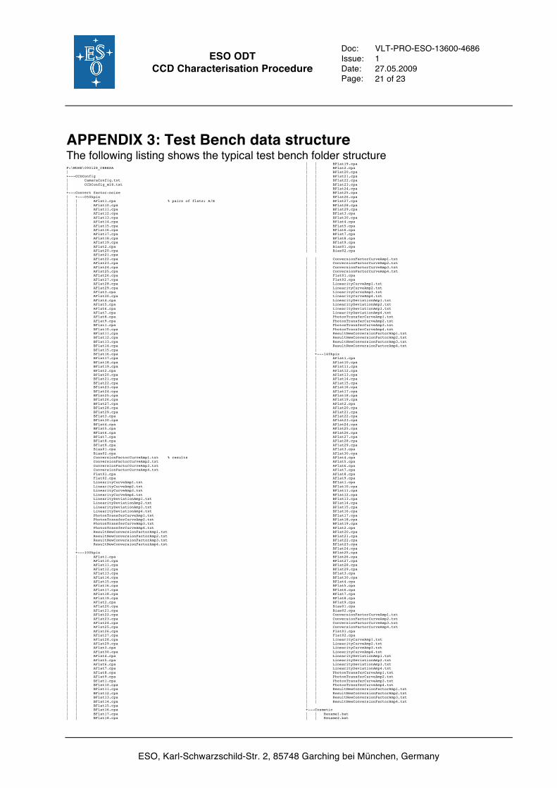
APPENDIX 3: Test Bench data structure The following listing shows the typical test bench folder structure F:\MUSE\090128_CERESA | +---CCDConfig | CameraConfig.txt | CCDConfig_m18.txt | +---Convert factor-noise | +---050kpix | | AFlat1.cpa % pairs of flats: A/B | | AFlat10.cpa | | AFlat11.cpa | | AFlat12.cpa | | AFlat13.cpa | | AFlat14.cpa | | AFlat15.cpa | | AFlat16.cpa | | AFlat17.cpa | | AFlat18.cpa | | AFlat19.cpa | | AFlat2.cpa | | AFlat20.cpa | | AFlat21.cpa | | AFlat22.cpa | | AFlat23.cpa | | AFlat24.cpa | | AFlat25.cpa | | AFlat26.cpa | | AFlat27.cpa | | AFlat28.cpa | | AFlat29.cpa | | AFlat3.cpa | | AFlat30.cpa | | AFlat4.cpa | | AFlat5.cpa | | AFlat6.cpa | | AFlat7.cpa | | AFlat8.cpa | | AFlat9.cpa | | BFlat1.cpa | | BFlat10.cpa | | BFlat11.cpa | | BFlat12.cpa | | BFlat13.cpa | | BFlat14.cpa | | BFlat15.cpa | | BFlat16.cpa | | BFlat17.cpa | | BFlat18.cpa | | BFlat19.cpa | | BFlat2.cpa | | BFlat20.cpa | | BFlat21.cpa | | BFlat22.cpa | | BFlat23.cpa | | BFlat24.cpa | | BFlat25.cpa | | BFlat26.cpa | | BFlat27.cpa | | BFlat28.cpa | | BFlat29.cpa | | BFlat3.cpa | | BFlat30.cpa | | BFlat4.cpa | | BFlat5.cpa | | BFlat6.cpa | | BFlat7.cpa | | BFlat8.cpa | | BFlat9.cpa | | Bias01.cpa | | Bias02.cpa | | ConversionFactorCurveAmp1.txt % results | | ConversionFactorCurveAmp2.txt | | ConversionFactorCurveAmp3.txt | | ConversionFactorCurveAmp4.txt | | Flat01.cpa | | Flat02.cpa | | LinearityCurveAmp1.txt | | LinearityCurveAmp2.txt | | LinearityCurveAmp3.txt | | LinearityCurveAmp4.txt | | LinearityDeviationAmp1.txt | | LinearityDeviationAmp2.txt | | LinearityDeviationAmp3.txt | | LinearityDeviationAmp4.txt | | PhotonTransferCurveAmp1.txt | | PhotonTransferCurveAmp2.txt | | PhotonTransferCurveAmp3.txt | | PhotonTransferCurveAmp4.txt | | ResultNewConversionFactorAmp1.txt | | ResultNewConversionFactorAmp2.txt | | ResultNewConversionFactorAmp3.txt | | ResultNewConversionFactorAmp4.txt | | | +---100kpix | | AFlat1.cpa | | AFlat10.cpa | | AFlat11.cpa | | AFlat12.cpa | | AFlat13.cpa | | AFlat14.cpa | | AFlat15.cpa | | AFlat16.cpa | | AFlat17.cpa | | AFlat18.cpa | | AFlat19.cpa | | AFlat2.cpa | | AFlat20.cpa | | AFlat21.cpa | | AFlat22.cpa | | AFlat23.cpa | | AFlat24.cpa | | AFlat25.cpa | | AFlat26.cpa | | AFlat27.cpa | | AFlat28.cpa | | AFlat29.cpa | | AFlat3.cpa | | AFlat30.cpa | | AFlat4.cpa | | AFlat5.cpa | | AFlat6.cpa | | AFlat7.cpa | | AFlat8.cpa | | AFlat9.cpa | | BFlat1.cpa | | BFlat10.cpa | | BFlat11.cpa | | BFlat12.cpa | | BFlat13.cpa | | BFlat14.cpa | | BFlat15.cpa | | BFlat16.cpa | | BFlat17.cpa | | BFlat18.cpa
| | BFlat19.cpa | | BFlat2.cpa | | BFlat20.cpa | | BFlat21.cpa | | BFlat22.cpa | | BFlat23.cpa | | BFlat24.cpa | | BFlat25.cpa | | BFlat26.cpa | | BFlat27.cpa | | BFlat28.cpa | | BFlat29.cpa | | BFlat3.cpa | | BFlat30.cpa | | BFlat4.cpa | | BFlat5.cpa | | BFlat6.cpa | | BFlat7.cpa | | BFlat8.cpa | | BFlat9.cpa | | Bias01.cpa | | Bias02.cpa | | ConversionFactorCurveAmp1.txt | | ConversionFactorCurveAmp2.txt | | ConversionFactorCurveAmp3.txt | | ConversionFactorCurveAmp4.txt | | Flat01.cpa | | Flat02.cpa | | LinearityCurveAmp1.txt | | LinearityCurveAmp2.txt | | LinearityCurveAmp3.txt | | LinearityCurveAmp4.txt | | LinearityDeviationAmp1.txt | | LinearityDeviationAmp2.txt | | LinearityDeviationAmp3.txt | | LinearityDeviationAmp4.txt | | PhotonTransferCurveAmp1.txt | | PhotonTransferCurveAmp2.txt | | PhotonTransferCurveAmp3.txt | | PhotonTransferCurveAmp4.txt | | ResultNewConversionFactorAmp1.txt | | ResultNewConversionFactorAmp2.txt | | ResultNewConversionFactorAmp3.txt | | ResultNewConversionFactorAmp4.txt | | | +---140kpix | | AFlat1.cpa | | AFlat10.cpa | | AFlat11.cpa | | AFlat12.cpa | | AFlat13.cpa | | AFlat14.cpa | | AFlat15.cpa | | AFlat16.cpa | | AFlat17.cpa | | AFlat18.cpa | | AFlat19.cpa | | AFlat2.cpa | | AFlat20.cpa | | AFlat21.cpa | | AFlat22.cpa | | AFlat23.cpa | | AFlat24.cpa | | AFlat25.cpa | | AFlat26.cpa | | AFlat27.cpa | | AFlat28.cpa | | AFlat29.cpa | | AFlat3.cpa | | AFlat30.cpa | | AFlat4.cpa | | AFlat5.cpa | | AFlat6.cpa | | AFlat7.cpa | | AFlat8.cpa | | AFlat9.cpa | | BFlat1.cpa | | BFlat10.cpa | | BFlat11.cpa | | BFlat12.cpa | | BFlat13.cpa | | BFlat14.cpa | | BFlat15.cpa | | BFlat16.cpa | | BFlat17.cpa | | BFlat18.cpa | | BFlat19.cpa | | BFlat2.cpa | | BFlat20.cpa | | BFlat21.cpa | | BFlat22.cpa | | BFlat23.cpa | | BFlat24.cpa | | BFlat25.cpa | | BFlat26.cpa | | BFlat27.cpa | | BFlat28.cpa | | BFlat29.cpa | | BFlat3.cpa | | BFlat30.cpa | | BFlat4.cpa | | BFlat5.cpa | | BFlat6.cpa | | BFlat7.cpa | | BFlat8.cpa | | BFlat9.cpa | | Bias01.cpa | | Bias02.cpa | | ConversionFactorCurveAmp1.txt | | ConversionFactorCurveAmp2.txt | | ConversionFactorCurveAmp3.txt | | ConversionFactorCurveAmp4.txt | | Flat01.cpa | | Flat02.cpa | | LinearityCurveAmp1.txt | | LinearityCurveAmp2.txt | | LinearityCurveAmp3.txt | | LinearityCurveAmp4.txt | | LinearityDeviationAmp1.txt | | LinearityDeviationAmp2.txt | | LinearityDeviationAmp3.txt | | LinearityDeviationAmp4.txt | | PhotonTransferCurveAmp1.txt | | PhotonTransferCurveAmp2.txt | | PhotonTransferCurveAmp3.txt | | PhotonTransferCurveAmp4.txt | | ResultNewConversionFactorAmp1.txt | | ResultNewConversionFactorAmp2.txt | | ResultNewConversionFactorAmp3.txt | | ResultNewConversionFactorAmp4.txt | +---Cosmetic | | Rename1.bat | | Rename2.bat

ESO ODT
CCD Characterisation Procedure
Doc: Issue: Date: Page:
VLT-PRO-ESO-13600-4686 1 27.05.2009 22 of 23
ESO, Karl-Schwarzschild-Str. 2, 85748 Garching bei München, Germany
| | | +---050kpix | \---100kpix | FlatLG350nm-1.cpa | FlatLG350nm-2.cpa | FlatLG475nm-1.cpa | FlatLG475nm-2.cpa | FlatLG600nm-1.cpa | FlatLG600nm-2.cpa | FlatLG750nm-1.cpa | FlatLG750nm-2.cpa | FlatLG900nm-1.cpa | FlatLG900nm-2.cpa | LowLevelFlatLG350nm-1.cpa | LowLevelFlatLG350nm-2.cpa | LowLevelFlatLG475nm-1.cpa | LowLevelFlatLG475nm-2.cpa | LowLevelFlatLG600nm-1.cpa | LowLevelFlatLG600nm-2.cpa | LowLevelFlatLG750nm-1.cpa | LowLevelFlatLG750nm-2.cpa | LowLevelFlatLG900nm-1.cpa | LowLevelFlatLG900nm-2.cpa | Result010209.txt | Result300109.txt | +---CosmeticDefect % TBD +---Cte | ResultAmp1.txt % result | +---Dark-Bias High Gain | | Rename.bat | | | +---050kpix | | +---Bias | | | Bias_HG_050kpix_Ceres1A-Ceres2A-1.cpa | | | Bias_HG_050kpix_Ceres1A-Ceres2A-2.cpa | | | Bias_HG_050kpix_Ceres1A-Ceres2A-3.cpa | | | Bias_HG_050kpix_Ceres1A-Ceres2A-4.cpa | | | Bias_HG_050kpix_Ceres1A-Ceres2A-5.cpa | | | | | +---DarkFifteenMinutes | | | Dark_HG_050kpix_FifteenMinutes_Ceres1A-Ceres2A-1.cpa | | | Dark_HG_050kpix_FifteenMinutes_Ceres1A-Ceres2A-2.cpa | | | Dark_HG_050kpix_FifteenMinutes_Ceres1A-Ceres2A-3.cpa | | | Dark_HG_050kpix_FifteenMinutes_Ceres1A-Ceres2A-4.cpa | | | Dark_HG_050kpix_FifteenMinutes_Ceres1A-Ceres2A-5.cpa | | | | | \---DarkOneHour | | Dark_HG_050kpix_OneHour_Ceres1A-Ceres2A-1.cpa | | Dark_HG_050kpix_OneHour_Ceres1A-Ceres2A-2.cpa | | Dark_HG_050kpix_OneHour_Ceres1A-Ceres2A-3.cpa | | Dark_HG_050kpix_OneHour_Ceres1A-Ceres2A-4.cpa | | Dark_HG_050kpix_OneHour_Ceres1A-Ceres2A-5.cpa | | | +---100kpix % file names wrong! 225 should be 100 | | +---Bias | | | Bias_HG_225kpix_Ceres1A-Ceres2A-1.cpa | | | Bias_HG_225kpix_Ceres1A-Ceres2A-2.cpa | | | Bias_HG_225kpix_Ceres1A-Ceres2A-3.cpa | | | Bias_HG_225kpix_Ceres1A-Ceres2A-4.cpa | | | Bias_HG_225kpix_Ceres1A-Ceres2A-5.cpa | | | | | +---DarkFifteenMinutes | | | Dark_HG_225kpix_FifteenMinutes_Ceres1A-Ceres2A-1.cpa | | | Dark_HG_225kpix_FifteenMinutes_Ceres1A-Ceres2A-2.cpa | | | Dark_HG_225kpix_FifteenMinutes_Ceres1A-Ceres2A-3.cpa | | | Dark_HG_225kpix_FifteenMinutes_Ceres1A-Ceres2A-4.cpa | | | Dark_HG_225kpix_FifteenMinutes_Ceres1A-Ceres2A-5.cpa | | | | | \---DarkOneHour | | Bias_HG_225kpix_Ceres1A-Ceres2A-5.cpa | | Dark_HG_225kpix_OneHour_Ceres1A-Ceres2A-1.cpa | | Dark_HG_225kpix_OneHour_Ceres1A-Ceres2A-2.cpa | | Dark_HG_225kpix_OneHour_Ceres1A-Ceres2A-3.cpa | | Dark_HG_225kpix_OneHour_Ceres1A-Ceres2A-4.cpa | | Dark_HG_225kpix_OneHour_Ceres1A-Ceres2A-5.cpa | | Mean_Bias.cpa | | ResultDarkCurrent.txt | +---Dark-Bias Low gain | | DarkCurrentScriptResult.txt | | Rename.bat | | | +---050kpix | | +---Bias | | +---DarkFifteenMinutes | | \---DarkOneHour | +---100kpix % file names wrong! 225 should be 100 | | +---Bias | | | Bias_LG_225kpix_Ceres1A-Ceres2A-1.cpa | | | Bias_LG_225kpix_Ceres1A-Ceres2A-2.cpa | | | Bias_LG_225kpix_Ceres1A-Ceres2A-3.cpa | | | Bias_LG_225kpix_Ceres1A-Ceres2A-4.cpa | | | Bias_LG_225kpix_Ceres1A-Ceres2A-5.cpa | | | | | +---DarkFifteenMinutes | | | Dark_LG_225kpix_FifteenMinutes_Ceres1A-Ceres2A-1.cpa | | | Dark_LG_225kpix_FifteenMinutes_Ceres1A-Ceres2A-2.cpa | | | Dark_LG_225kpix_FifteenMinutes_Ceres1A-Ceres2A-3.cpa | | | Dark_LG_225kpix_FifteenMinutes_Ceres1A-Ceres2A-4.cpa | | | Dark_LG_225kpix_FifteenMinutes_Ceres1A-Ceres2A-5.cpa | | | | | \---DarkOneHour | | Dark_LG_225kpix_OneHour_Ceres1A-Ceres2A-1.cpa | | Dark_LG_225kpix_OneHour_Ceres1A-Ceres2A-2.cpa | | Dark_LG_225kpix_OneHour_Ceres1A-Ceres2A-3.cpa | | Dark_LG_225kpix_OneHour_Ceres1A-Ceres2A-4.cpa | | Dark_LG_225kpix_OneHour_Ceres1A-Ceres2A-5.cpa | | | \---625kpix % used if needed | +---Bias | +---DarkFifteenMinutes | \---DarkOneHour +---HTML-files | | Cosmetic.html | | DarkAndBias.html | | DarkHG1h.jpg | | ESOTestReport.html | | FlatHG475nm-2.jpg | | FlatHG750nm-2.jpg | | FlatHG900nm-2.jpg | | Linearity.html | | MaconiTestReport.html | | NomDuCCD.html | | | +---Images | \---ImagesMeasurement +---Linearity % measured above +---LowGainFlat +---Observations | Observations.rtf | +---Pocket pumping % used if needed +---PSFFile % TBD +---Qe | +---Qe | | 1000.cpa | | 1020.cpa | | 1040.cpa | | 1060.cpa | | 1080.cpa | | 1100.cpa | | 300.cpa | | 310.cpa
| | 320.cpa | | 330.cpa | | 340.cpa | | 350.cpa | | 360.cpa | | 370.cpa | | 380.cpa | | 390.cpa | | 400.cpa | | 420.cpa | | 440.cpa | | 460.cpa | | 480.cpa | | 500.cpa | | 520.cpa | | 540.cpa | | 560.cpa | | 580.cpa | | 600.cpa | | 620.cpa | | 640.cpa | | 660.cpa | | 680.cpa | | 700.cpa | | 720.cpa | | 740.cpa | | 760.cpa | | 780.cpa | | 800.cpa | | 820.cpa | | 840.cpa | | 860.cpa | | 880.cpa | | 900.cpa | | 920.cpa | | 940.cpa | | 960.cpa | | 980.cpa | | Bias01.cpa | | Bias02.cpa | | Flat01.cpa | | Flat02.cpa | | MedianBias.cpa | | resultQE.txt | | resultQEDebug.txt | | resultQEDebugRev.txt | | resultQERev.txt | | resultQE_060409.txt | | Rev1000.cpa % reverse, if needed, can be ignored | | Rev1020.cpa | | Rev1040.cpa | | Rev1060.cpa | | Rev1080.cpa | | Rev1100.cpa | | Rev300.cpa | | Rev310.cpa | | Rev320.cpa | | Rev330.cpa | | Rev340.cpa | | Rev350.cpa | | Rev360.cpa | | Rev370.cpa | | Rev380.cpa | | Rev390.cpa | | Rev400.cpa | | Rev420.cpa | | Rev440.cpa | | Rev460.cpa | | Rev480.cpa | | Rev500.cpa | | Rev520.cpa | | Rev540.cpa | | Rev560.cpa | | Rev580.cpa | | Rev600.cpa | | Rev620.cpa | | Rev640.cpa | +---ScriptPRiSM % scripts used by test bench for | | CosmeticDefect.pgm % data acquisition and evaluation | | CreateVoltageTable_20061114.pgm | | DarkAc_emmiRed_170109.pgm | | DarkAc_emmiRed_240409.pgm | | DarkAc_miteev_Uvesr_240304.pgm | | DarkAc_MUSE_170109.pgm | | DarkAndBiasAcquisition_tbmit.pgm | | DarkCurrent.pgm | | DarkCurrent_MUSE.pgm | | EditCCDConfig_20061112.pgm | | Eric_TestAutomDataAcq_CCDAlignment.pgm | | Eric_TestAutomDataAcq_CCDAlignment02(InProgress).pgm | | Eric_TestAutomDataAcq_CCDAlignment02(InProgress)old.pgm | | Eric_TestAutomDataAcq_CCDAlignment03(InProgress).pgm | | First noise results.txt | | FirstResult040209.txt | | FirstResult040209_shortBandwdth.txt | | FirstResult040209_Step2.txt | | FirstResult040209_Step3.txt | | FirstResult280109.txt | | FirstResult50kpixNoise_170209.txt | | InfoDark.txt | | InfoDarkBackup.txt | | InfoLight.txt | | InfoLight.txt.old | | InfoLightBackup.txt | | InfoLightBackup.txt.old | | InfoLightMarkSpecial.txt | | InfoOptimize.txt | | LightAc_All_030409_emmiRed_FIERA_051_PT.pgm | | LightAc_All_030409_muse_NGCPc012473_PT.pgm | | LightAc_All_070108.pgm | | LightAc_All_080108.pgm | | LightAc_All_081208_MUSE_NGC_Pc012473.pgm | | LightAc_All_090108.pgm | | LightAc_All_100108.pgm | | LightAc_All_110108.pgm | | LightAc_All_120108_225BIN8.pgm | | LightAc_All_120108_225BIN8COS225.pgm | | LightAc_All_120309_emmiRed_FIERA_051_PT.pgm | | LightAc_All_120309_muse_NGCPc012473_PT.pgm | | LightAc_All_121208c_emmi_FIERA_Lapodt2.pgm | | LightAc_All_121208c_MUSE_FIERALapodt2.pgm | | LightAc_All_121208c_MUSE_FIERAPc012473.pgm | | LightAc_All_121208c_MUSE_NGC_Pc012473.pgm | | LightAc_All_131208e_emmiRed_FIERALapodt2.pgm | | LightAc_All_131208e_muse_NGC_Pc012473.pgm | | LightAc_All_160109_emmiRed_FIERALapodt2.pgm | | LightAc_All_160109_muse_NGCPc012473.pgm | | LightAc_All_160109_muse_NGCPc012473_PT.pgm | | LightAc_All_170209_muse_NGCPc012473_PT.pgm | | LightAc_All_171208_emmiRed_FIERALapodt2.pgm | | LightAc_All_171208_emmiRed_FIERALapodt2HG.pgm | | LightAc_All_250408.pgm | | LightAc_All_250408_225BIN8COS225.pgm | | LightAc_All_250408_MUSE_NGC_111108.pgm | | LightAc_All_250408_MUSE_NGC_220708.pgm | | LightAc_All_250408_MUSE_NGC_271008.pgm | | LightAc_All_250408_MUSE_NGC_281008.pgm | | LightAc_All_250408_MUSE_NGC_281008b.pgm | | LightAc_All_250408_MUSE_NGC_281008d.pgm | | LightAc_All_250408_MUSE_NGC_281008less10.pgm | | LightAc_All_250409_emmiRed_FIERA_051_PT.pgm | | LightAc_miteev_DM_All_030108.pgm | | LightAc_miteev_DM_All_040108.pgm | | LightAc_miteev_DM_All_050108.pgm

ESO ODT
CCD Characterisation Procedure
Doc: Issue: Date: Page:
VLT-PRO-ESO-13600-4686 1 27.05.2009 23 of 23
ESO, Karl-Schwarzschild-Str. 2, 85748 Garching bei München, Germany
| | LightAc_miteev_DM_All_050108_TEST.pgm | | LightAc_miteev_DM_All_060108.pgm | | LightAc_miteev_DM_AO_031207.pgm | | LightAc_miteev_DM_AO_201107.pgm | | LightAc_miteev_DM_AO_211107.pgm | | LightAc_miteev_DM_AO_221107.pgm | | LightAc_miteev_DM_AO_221107a.pgm | | LightAc_miteev_DM_AO_221107a_only225.pgm | | LightAc_miteev_DM_AO_221107QE_énderung.pgm | | LightAc_miteev_DM_AO_271107.pgm | | Linearity.pgm | | Linearity2.pgm | | PnSensor_LightAc_200607.pgm | | PSF_20061113.pgm | | PSF_new motors_E2V_CCDB_sd150506_700nm.pgm | | result111108.txt | | result121108.txt | | Result300109.txt | | Result300109b.txt | | ResultConversionFactorNoise170209.txt | | ResultDark040209.txt | | ResultDark050209.txt | | ResultDark060209.txt | | Second noise results.txt | | SecondBResult040209.txt | | SecondResult.txt | | SecondResult040209.txt | | SecondResult290109.txt | | Test_AO_LabView_PRiSM_271107.pgm | | | +---CalibrationFile % test bench calibration files | | CalibrationFile.txt | | CalibrationFile.txt_041207 | | CalibrationFile.txt_211107 | | CalibrationFile.txt_271107 | | CalibrationFile_AO211107.txt | | CalibrationFile_short.txt | | Copy of CalibrationFile.txt | | Ratio_041207.txt | | Ratio_106.txt_211107 | | Ratio_271107.txt | | WindowTransmission.txt | | WindowTransmission_short.txt | | | \---ScriptToCalibrateTestBench | calibrate.pgm | calibrateAO.pgm | CalibrationReferrence_hamamatsu1_06.txt | CalibrationReferrence_june2001.txt | CalibrationReferrence_NPL106.txt | FinalResult_AO_041207.txt | FinalResult_AO_211107.txt | FinalResult_AO_271107.txt | Hama106_CalibrationReferrence.txt | Ratio_106__AO_211107.txt | \---VoltTable
End of document