CC120X Low-Power High Performance Sub-1 GHz … · CC120X Low-Power High Performance Sub-1 GHz RF...
115
CC120X SWRU346B Page 1 of 114 CC120X Low-Power High Performance Sub-1 GHz RF Transceivers User’s Guide
Transcript of CC120X Low-Power High Performance Sub-1 GHz … · CC120X Low-Power High Performance Sub-1 GHz RF...

CC120X
SWRU346B Page 1 of 114
CC120X Low-Power High Performance
Sub-1 GHz RF Transceivers
User’s Guide

CC120X
SWRU346B Page 2 of 114
Abbreviations
Abbreviations used in this data sheet are described below.
2-FSK Binary Frequency Shift Keying LO Local Oscillator
4-FSK Quaternary Frequency Shift Keying LSB Least Significant Bit
ACP Adjacent Channel Power LQI Link Quality Indicator
ADC Analog to Digital Converter MCU Microcontroller Unit
AES Advanced Encryption Standard MSB Most Significant Bit
AFC Automatic Frequency Compensation MSK Minimum Shift Keying
AGC Automatic Gain Control NRNSC Non-recursive Non-systematic Convolutional
ASK Amplitude Shift Keying OOK On-Off Keying
BIST Built-In Self-Test PA Power Amplifier
BT Bandwidth-Time Product PD Power Down
CCA Clear Channel Assessment PER Packet Error Rate
CRC Cyclic Redundancy Check PLL Phase Locked Loop
CS Carrier Sense POR Power-On Reset
DC Direct Current PQT Preamble Quality Threshold
CFM Custom Frequency Modulation PTAT Proportional to Absolute Temperature
ESR Equivalent Series Resistance QPSK Quadrature Phase Shift Keying
FCC Federal Communications Commission RC Resistor-Capacitor
FEC Forward Error Correction RF Radio Frequency
FIFO First-In-First-Out RSSI Received Signal Strength Indicator
FHSS Frequency Hopping Spread Spectrum RX Receive, Receive Mode
FS Frequency Synthesizer RXDCM RX Duty Cycle Mode
GFSK Gaussian shaped Frequency Shift Keying SPI Serial Peripheral Interface
GPIO General Purpose Input/Output SRD Short Range Devices
IF Intermediate Frequency TX Transmit, Transmit Mode
I/Q In-Phase/Quadrature VCO Voltage Controlled Oscillator
ISM Industrial, Scientific, Medical eWOR Enhanced Wake on Radio
kbps kilo bit per second XOSC Crystal Oscillator
ksps kilo symbol per second XTAL Crystal
LNA Low Noise Amplifier

CC120X
SWRU346B Page 3 of 114
Table of Contents
ABBREVIATIONS ............................................................................................................................................... 2
TABLE OF CONTENTS ..................................................................................................................................... 3
1 OVERVIEW .............................................................................................................................................. 5
2 CONFIGURATION SOFTWARE .......................................................................................................... 6
3 MICROCONTROLLER INTERFACE ................................................................................................. 7 3.1 CONFIGURATION ......................................................................................................................................... 7 3.2 SPI ACCESS TYPES ...................................................................................................................................... 9 3.3 OPTIONAL PIN CTRL RADIO CONTROL FEATURE .................................................................................... 17 3.4 GENERAL PURPOSE INPUT/OUTPUT CONTROL PINS .................................................................................. 17
4 ON-CHIP TEMPERATURE SENSOR ................................................................................................ 22
5 COMMON RECEIVE AND TRANSMIT CONFIGURATIONS ...................................................... 23 5.1 DATA COMMUNICATION MODES ............................................................................................................... 23 5.2 MODULATION FORMATS ............................................................................................................................ 24 5.3 FORWARD ERROR CORRECTION ................................................................................................................ 29 5.4 SYMBOL RATE PROGRAMMING ................................................................................................................. 29
6 RECEIVE CONFIGURATION ............................................................................................................ 30 6.1 RX FILTER BANDWIDTH ............................................................................................................................ 30 6.2 DC OFFSET REMOVAL ............................................................................................................................... 31 6.3 FEEDBACK TO PLL .................................................................................................................................... 32 6.4 AUTOMATIC GAIN CONTROL ..................................................................................................................... 33 6.5 IMAGE COMPENSATION ............................................................................................................................. 34 6.6 BIT SYNCHRONIZATION ............................................................................................................................. 35 6.7 BYTE SYNCHRONIZATION, SYNC WORD DETECTION ................................................................................. 35 6.8 PREAMBLE DETECTION ............................................................................................................................. 36 6.9 RSSI .......................................................................................................................................................... 37 6.10 COLLISION DETECTOR ............................................................................................................................... 42 6.11 CLEAR CHANNEL ASSESSMENT (CCA) ..................................................................................................... 42 6.12 LISTEN BEFORE TALK (LBT) .................................................................................................................... 43 6.13 LINK QUALITY INDICATOR (LQI) .............................................................................................................. 43
7 TRANSMIT CONFIGURATION ......................................................................................................... 44 7.1 PA OUTPUT POWER PROGRAMMING ......................................................................................................... 44 7.2 OOK/ASK BIT SHAPING ........................................................................................................................... 45
8 PACKET HANDLING HARDWARE SUPPORT .............................................................................. 46 8.1 STANDARD PACKET FORMAT .................................................................................................................... 46 8.2 PACKET FILTERING IN RECEIVE MODE ...................................................................................................... 52 8.3 PACKET HANDLING IN TRANSMIT MODE ................................................................................................... 53 8.4 PACKET HANDLING IN RECEIVE MODE ..................................................................................................... 53 8.5 PACKET HANDLING IN FIRMWARE ............................................................................................................. 53 8.6 TX FIFO AND RX FIFO ............................................................................................................................ 54 8.7 IEEE 802.15.4G SUPPORT ......................................................................................................................... 55 8.8 802.15.4G FRAME CHECK SEQUENCE (FCS) ............................................................................................. 59 8.9 TRANSPARENT AND SYNCHRONOUS SERIAL OPERATION .......................................................................... 59
9 RADIO CONTROL ................................................................................................................................ 62 9.1 POWER-ON START-UP SEQUENCE ............................................................................................................. 62 9.2 CRYSTAL CONTROL ................................................................................................................................... 62 9.3 VOLTAGE REGULATOR CONTROL .............................................................................................................. 62 9.4 ACTIVE MODES ......................................................................................................................................... 63 9.5 RX TERMINATION ..................................................................................................................................... 64 9.6 ENHANCED WAKE ON RADIO (EWOR) ...................................................................................................... 67 9.7 RX SNIFF MODE ........................................................................................................................................ 70 9.8 RX DUTY CYCLE MODE ............................................................................................................................ 72 9.9 RC OSCILLATOR CALIBRATION ................................................................................................................. 73 9.10 ANTENNA DIVERSITY AND MULTIPLE PATH TRANSMISSION ..................................................................... 73 9.11 RANDOM NUMBER GENERATOR ................................................................................................................ 74 9.12 RF PROGRAMMING .................................................................................................................................... 74 9.13 FREQUENCY SYNTHESIZER CONFIGURATION............................................................................................. 75

CC120X
SWRU346B Page 4 of 114
9.14 IF PROGRAMMING ..................................................................................................................................... 75 9.15 FS CALIBRATION ....................................................................................................................................... 76 9.16 FS OUT OF LOCK DETECTION .................................................................................................................... 76
10 AES .......................................................................................................................................................... 77 10.1 AES BLOCK OPERATION ........................................................................................................................... 77 10.2 AES COMMANDS....................................................................................................................................... 77 10.3 AES PARAMETERS .................................................................................................................................... 77 10.4 AES TX/RXFIFO OPERATION .................................................................................................................. 78
11 SYSTEM CONSIDERATIONS AND GUIDELINES ......................................................................... 79 11.1 VOLTAGE REGULATORS ............................................................................................................................ 79 11.2 SRD REGULATIONS ................................................................................................................................... 79 11.3 FREQUENCY HOPPING AND MULTI-CHANNEL SYSTEMS ............................................................................ 79 11.4 CONTINUOUS TRANSMISSIONS .................................................................................................................. 79 11.5 BATTERY OPERATED SYSTEMS ................................................................................................................. 79
12 REGISTER DESCRIPTION ................................................................................................................. 80
13 SOLDERING INFORMATION .......................................................................................................... 114
14 DEVELOPMENT KIT ORDERING INFORMATION ................................................................... 114
15 REFERENCES ..................................................................................................................................... 114
16 GENERAL INFORMATION .............................................................................................................. 114 16.1 DOCUMENT HISTORY .............................................................................................................................. 114

CC120X
SWRU346B Page 5 of 114
1 Overview
CC120X is a family of high performance low power RF transceivers designed for operation with a companion MCU. The purpose of this user’s guide is to describe configurations and functionality
available for implementing a wireless system. CC120X automates all common RF related tasks, greatly offloading the MCU. Below is a block diagram showing the different parts of the transceiver divided in an RF related part and a part for digital support functionality.
BIAS
RB
IAS
XO
SC_Q
1
XO
SC_Q
2
XOSC
LNA
0
90
FREQ
SYNTH
ADC
ADC
DE
MO
DU
LA
TO
R
PA
CK
ET
HA
ND
LE
R
RX
FIF
O
MO
DU
LA
TO
R
TX
FIF
O
RADIO CONTROL & POWER MANAGEMENT
LNA_P
LNA_N
PA
EXT_
XO
SC
PALF
C1
CS_N
SI
SO (GPIO0)
SCLK
GPIO2
GPIO1
GPIO3
DIG
ITA
L IN
TE
RF
AC
E T
O M
CU
LFC
0
CC120x
MARC
Main Radio Control unit
Ultra low power 16 bit
MCU
256 byte
FIFO RAM
buffer
4 kbyte
ROM
RF and DSP frontend
Packet handler
and FIFO controlConfiguration and
status registers
eWOR
Enhanced ultra low power
Wake On Radio timer
SPI
Serial configuration
and data interface
Interrupt and
IO handlerSystem bus
PA out
LNA_P
LNA_N
90 dB dynamic
range ADC
90 dB dynamic
range ADC
High linearity
LNA
14 dBm high
efficiency PA
Ch
an
ne
l
filte
r
XOSC
Co
rdic
AGC
Automatic Gain Control, 60dB VGA range
RSSI measurements and carrier sense detection
Highly flexible FSK / OOK
demodulator
(optional bit clock)
(optional low jitter serial
data output for legacy
protocols)
Data interface with
signal chain access
XOSC_Q1
XOSC_Q2
Ultra low power 40 kHz
auto-calibrated RC oscillator(optional 40 kHz
clock intput)
CSn (chip select)
SI (serial input)
SO (serial output)
SCLK (serial clock)
(optional GPIO3/2/0
Mo
du
lato
r
Fully integrated fractional-N
frequency synthesizer
Output power ramping and OOK / ASK modulation
IF amp
IF amp
(optional auto detected
external XOSC / TCXO)
(optional GPIO for
antenna diversity)
I
Q
Battery sensor /
temp sensor
Power on reset
AES-128
accelerator
Figure 1: CC120X Block Diagram
CC120X can be configured to achieve optimum performance for many different applications using the SPI interface (see Section 3.1.1 for more details). The following key parameters can be programmed:
Power-down/power-up mode (SLEEP/IDLE)
Crystal oscillator power-up/power-down (IDLE/XOFF)
Receive/transmit mode (RX/TX)
Carrier frequency
Symbol rate
Modulation format
RX channel filter bandwidth
RF output power
Data buffering with separate 128-byte receive and transmit FIFOs
Packet radio hardware support
Data whitening
Enhanced Wake-On-Radio (eWOR)
Figure 1 shows a simplified state diagram. For detailed information on controlling the CC120X state machine see Section 9.

CC120X
SWRU346B Page 6 of 114
Transmit mode Receive mode
IDLE
Manual freq.
synth. calibration
RX FIFO
ERROR
TX FIFO
ERROR
Frequency
synthesizer on
SFSTXON
SRX or wake-on-radio (WOR)
STX
STX
STX or RXOFF_MODE=10
RXOFF_MODE = 00
SFTX
SRX or TXOFF_MODE = 11
SIDLE
SCAL
SFRX
IDLE
TXOFF_MODE = 00
SFSTXON or RXOFF_MODE = 01
SRX or STX or SFSTXON or wake-on-radio (WOR)
SLEEP
SPWD or wake-on-radio (WOR)
Crystal
oscillator off
SXOFF
CSn = 0
CSn = 0
TXOFF_MODE = 01
Frequency
synthesizer startup,
optional calibration,
settling
Optional freq.
synth. calibration
Default state when the radio is not
receiving or transmitting.
Lowest power mode. Most
register values are retained
(see Table 5 for details ).
All register values are
retained.
Used for calibrating frequency
synthesizer upfront (entering
receive or transmit mode can
then be done quicker).
Transitional state.
Frequency synthesizer is turned on, can optionally be
calibrated, and then settles to the correct frequency.
Transitional state. Frequency synthesizer is on,
ready to start transmitting.
Transmission starts very
quickly after receiving the STX
command strobe.
Optional transitional state.
In FIFO-based modes,
transmission is turned off and
this state entered if the TX
FIFO becomes empty in the
middle of a packet.
In FIFO-based modes,
reception is turned off and this
state entered if the RX FIFO
overflows.
SRX
Figure 2: Simplified State Diagram
2 Configuration Software
CC112X can be configured using the SmartRF™ Studio software [1]. SmartRF Studio is highly recommended for obtaining optimum register settings, and for evaluating performance and functionality.
After chip reset, all registers have default values and these might differ from the optimum register setting. It is therefore necessary to configure/reconfigure the radio through the SPI interface after the chip has been reset. SmartRF Studio provides a code export function making it easy to implement this in firmware.

CC120X
SWRU346B Page 7 of 114
3 Microcontroller Interface
3.1 Configuration
In a typical system, CC120X will interface to an MCU. This MCU must be able to communicate with the
CC120X over a 4-wire SPI interface to be able to:
Configure the CC120X
Program CC120X into different modes (RX, TX, SLEEP, IDLE, etc)
Read and write buffered data (RX FIFO and TX FIFO)
Read status information
3.1.1 4-wire Serial Configuration and Data Interface
CC120X is configured via a simple 4-wire SPI-compatible interface (SI, SO, SCLK, and CSn) where
CC120X is the slave. This interface is also used to read and write buffered data. All transfers on the SPI interface are done most significant bit first.
All transactions on the SPI interface start with a header byte containing a R/W̄ bit, a burst access bit (B), and a 6-bit address (A5 - A0). A status byte is sent on the SO pin each time a header byte is transmitted on the SI pin (see Section 3.1.2 for more details on the chip status byte).
The CSn pin must be kept low during transfers on the SPI bus. The timing for the address and data transfers on the SPI interface is shown in Figure 3 with reference to Table 1.
0 B A5 A4 A3 A2 A1 A0 DW7 DW6 DW5 DW4 DW3 DW2 DW1 DW0X X
S7
tsp
S5 S4 S3 S2 S1 S0 S7 S6 S5 S4 S3 S2 S1 S0
Hi ZS0
X
Hi Z
1 B A5 A4 A3 A2 A1 A0X X
S7 S6 S5 S4 S3 S2 S1 S0 DR7 DR6 DR5 DR4 DR3 DR2 DR1 DR0S0
Hi Z
0
tch tcl tsd thd tns
SCLK
CSn
SI
SO
SI
SO
Write to Register
Read from Register
Hi Z
Figure 3: Configuration Registers Write and Read Operations
Parameter Description Min Max Units
fSCLK SCLK frequency read/write access Note: A 100 ns delay between consecutive data bytes must be added during burst write access to the configuration registers
- 10 MHz
SCLK frequency read access extended memory 7.7
tsp CSn low to positive edge on SCLK 50 - ns
tch Clock high 47.5 - ns
tcl Clock low 47.5 - ns
trise Clock rise time - 40 ns
tfall Clock fall time - 40 ns
tsd Setup data before a positive edge on SCLK 10 - ns
thd Hold data after positive edge on SCLK 10 - ns
tns Negative edge on SCLK to CSn high. 200 - ns
CSn high time, time from CSn has been pulled high until it can be pulled low again 50 ns
Table 1: SPI Timing Requirements

CC120X
SWRU346B Page 8 of 114
When CSn is pulled low, the MCU must wait until CC120X SO pin goes low before starting to transfer the header byte. This indicates that the crystal is stable. Unless the chip was just reset or was in SLEEP or XOFF state, or the XOSC configuration has been altered, the SO pin will always go low immediately after pulling CSn low.
Registers with consecutive addresses can be accessed in an efficient way by setting the burst bit (B) in the header byte. The address bits (A5 - A0) set the start address in an internal address counter. This counter is incremented by one each new byte (every 8 clock pulses). The burst access is either a read or write, and must be terminated by setting CSn high.
If a single register shall be accessed multiple times (e.g. CFM_RX_DATA_OUT/ CFM_TX_DATA_IN for
custom frequency modulation, see Section 5.2.4), the EXT_CTRL.BURST_ADDR_INCR_EN bit can be
set to 0. In this mode the address counter will not increment in burst mode, and it is possible to read/write the same register repeatedly without address overhead.
Table 3 gives an overview of the different SPI access types possible.
3.1.2 Chip Status Byte
When the header byte, data byte, or command strobe is sent on the SPI interface, the chip status byte
is sent by the CC120X on the SO pin. The status byte contains key status signals, useful for the MCU.
The first bit, S7, is the CHIP_RDYn signal and this signal must go low before the first positive edge of
SCLK. The CHIP_RDYn signal indicates that the crystal is stable.
S6, S5, and S4 comprise the STATE value which reflects the state of the chip. In IDLE state the XOSC
and power to the digital core are on and all other modules are in power down. Unless otherwise stated, registers should not be changed unless the chip is in this state.
Table 2 gives a status byte summary.
Bits Name Description
7 CHIP_RDYn Stays high until power and crystal have stabilized. Should always be low when using the SPI interface.
6:4 STATE[2:0] Indicates the current main state machine mode
Value State MARC State Description
000 IDLE IDLE IDLE state
001 RX RX RX_END
Receive mode
010 TX TX TX_END
Transmit mode
011 FSTXON FSTXON Fast TX ready
100 CALIBRATE BIAS_SETTLE_MC REG_SETTLE_MC MANCAL STARTCAL ENDCAL
Frequency synthesizer calibration is running
101 SETTLING BIAS_SETTLE REG_SETTLE BWBOOST FS_LOCK IFADCON RXTX_SWITCH TXRX_SWITCH IFADCON_TXRX
PLL is settling
110 RX FIFO ERROR
RX_FIFO_ERR RX FIFO has over/underflowed. Read out any useful data, then flush the FIFO with an
SFRX strobe
111 TX FIFO ERROR
TX_FIFO_ERR TX FIFO has over/underflowed. Flush the
FIFO with an SFTX strobe
3:0 Reserved
Table 2: Status Byte Summary
CC120X
SWRU346B Page 9 of 114
3.2 SPI Access Types
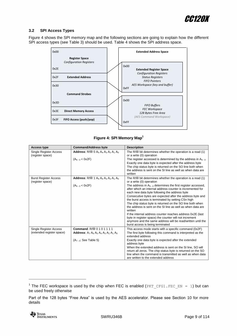
Figure 4 shows the SPI memory map and the following sections are going to explain how the different SPI access types (see Table 3) should be used. Table 4 shows the SPI address space.
0x00
Register SpaceConfiguration Registers
0x2E
Extended Address0x2F
0x30
0x3D
Command Strobes
Direct Memory Access0x3E
0x3F FIFO Access (push/pop)
0x00
0xFF
Extended Register SpaceConfiguration Registers
Status RegistersFIFO Pointers
AES Workspace (key and buffer)
0x00
0xFF
FIFO BuffersFEC Workspace
128 Bytes Free Area(AES Command Workspace)
Extended Address Space
Figure 4: SPI Memory Map1
Access type Command/Address byte Description
Single Register Access (register space)
Address: R/W̄ 0 A5 A4 A3 A2 A1 A0
(A5 - 0 < 0x2F)
The R/W̄ bit determines whether the operation is a read (1) or a write (0) operation
The register accessed is determined by the address in A5 - 0
Exactly one data byte is expected after the address byte
The chip status byte is returned on the SO line both when the address is sent on the SI line as well as when data are written
Burst Register Access (register space)
Address: R/W̄ 1 A5 A4 A3 A2 A1 A0
(A5 - 0 < 0x2F)
The R/W̄ bit determines whether the operation is a read (1) or a write (0) operation
The address in A5 - 0 determines the first register accessed, after which an internal address counter is incremented for each new data byte following the address byte
Consecutive bytes are expected after the address byte and the burst access is terminated by setting CSn high
The chip status byte is returned on the SO line both when the address is sent on the SI line as well as when data are written
If the internal address counter reaches address 0x2E (last byte in register space) the counter will not increment anymore and the same address will be read/written until the burst access is being terminated
Single Register Access (extended register space)
Command: R/W̄ 0 1 0 1 1 1 1
Address: A7 A6 A5 A4 A3 A2 A1 A0
(A7 - 0: See Table 5)
This access mode starts with a specific command (0x2F)
The first byte following this command is interpreted as the extended address
Exactly one data byte is expected after the extended address byte
When the extended address is sent on the SI line, SO will return all zeros. The chip status byte is returned on the SO line when the command is transmitted as well as when data are written to the extended address
1 The FEC workspace is used by the chip when FEC is enabled (PKT_CFG1.FEC_EN = 1) but can
be used freely otherwise
Part of the 128 bytes “Free Area” is used by the AES accelerator. Please see Section 10 for more details

CC120X
SWRU346B Page 10 of 114
Access type Command/Address byte Description
Burst Register Access (extended register space)
Command: R/W̄ 1 1 0 1 1 1 1
Address: A7 A6 A5 A4 A3 A2 A1 A0
(A7 - 0: See Table 5)
This access mode starts with a specific command (0x2F)
The first byte following this command is interpreted as the extended address
Consecutive bytes are expected after the extended address byte and the burst access is terminated by setting CSn high
When the extended address is sent on the SI line, SO will return all zeros. The chip status byte is returned on the SO line when the command is transmitted as well as when data are written to the extended address.
If the internal address counter reaches address 0xFF (last byte in extended register space) the counter will wrap around to 0x00
Registers not listed in Table 5 can be part of a burst access
Command Strobe Access Address: R/W̄ 0 A5 A4 A3 A2 A1 A0
(0x30 ≤ A5 - 0 ≤ 0x3D)
Accessing one of the command strobe registers triggers an event determined by the address in A5 - 0, e.g. resetting the device, enabling the crystal oscillator, entering TX, etc. No data byte is expected.
The chip status byte is returned on the SO line when a command strobe is sent on the SI line
Standard FIFO Access Address: R/W̄ B 1 1 1 1 1 1 The R/W̄ bit determines whether the operation is a read (1) operation from the RX FIFO or a write (0) operation to the TX FIFO. If the burst bit B is 1, all bytes following the address byte are treated as data bytes until CSn goes high. If the burst bit B is 0, the FIFOs are accessed byte-wise as a normal register.
Direct Access to FIFO Buffers
Command: R/W̄ B 1 1 1 1 1 0 Address: A7 A6 A5 A4 A3 A2 A1 A0
SPI_DIRECT_ACCESS_CFG in
SERIAL_STATUS must be 0
A7 - 0 < 0x80: TX FIFO 0x80 ≤ A7 - 0 ≤ 0xFF: RX FIFO
This access mode starts with a specific command (0x3E) which makes it possible to access the FIFOs directly through memory operations without affecting the FIFO pointers.
The first byte following this command is interpreted as the address. The next byte is read/written to this address. If burst is enabled, consecutive bytes will be read/written by incrementing the address.2
FIFO pointers are available in extended register space for debug purposes.
Direct Access to FEC Workspace
Command: R/W̄ B 1 1 1 1 1 0 Address: A7 A6 A5 A4 A3 A2 A1 A0
SPI_DIRECT_ACCESS_CFG in
SERIAL_STATUS must be 1
(A7 - 0 < 0x80)
This access mode starts with a specific command (0x3E) which makes it possible to access the FEC workspace.
The first byte following this command is interpreted as the address. The next byte is read/written to this address. If burst is enabled, consecutive bytes will be read/written by incrementing the address.
Direct Access to 128 Bytes Free Area (AES Command Workspace)
Command: R/W̄ B 1 1 1 1 1 0 Address: A7 A6 A5 A4 A3 A2 A1 A0
SPI_DIRECT_ACCESS_CFG in
SERIAL_STATUS must be 1
0x80 ≤ A7 - 0 ≤ 0xFF
This access mode starts with a specific command (0x3E) which makes it possible to access 128 bytes of free memory.
The first byte following this command is interpreted as the address. The next byte is read/written to this address. If burst is enabled, consecutive bytes will be read/written by incrementing the address.
Table 3: SPI Access Types
2 Note that the first byte received in an empty RX FIFO will not be possible to read using direct FIFO
access but can be read from extended register space (A7 – 0 = 0xDA). Please see Section 3.2.3 for more details.

CC120X
SWRU346B Page 11 of 114
Write Read
Single Byte Burst Single Byte Burst
+0x00 +0x40 +0x80 +0xC0
0x00 IOCFG3
R/W
config
ura
tio
n r
egis
ters
, burs
t access p
ossib
le
0x01 IOCFG2
0x02 IOCFG1
0x03 IOCFG0
0x04 SYNC3
0x05 SYNC2
0x06 SYNC1
0x07 SYNC0
0x08 SYNC_CFG1
0x09 SYNC_CFG0
0x0A DEVIATION_M
0x0B MODCFG_DEV_E
0x0C DCFILT_CFG
0x0D PREAMBLE_CFG1
0x0E PREAMBLE_CFG0
0x0F IQIC
0x10 CHAN_BW
0x11 MDMCFG1
0x12 MDMCFG0
0x13 SYMBOL_RATE2
0x14 SYMBOL_RATE1
0x15 SYMBOL_RATE0
0x16 AGC_REF
0x17 AGC_CS_THR
0x18 AGC_GAIN_ADJUST
0x19 AGC_CFG3
0x1A AGC_CFG2
0x1B AGC_CFG1
0x1C AGC_CFG0
0x1D FIFO_CFG
0x1E DEV_ADDR
0x1F SETTLING_CFG
0x20 FS_CFG
0x21 WOR_CFG1
0x22 WOR_CFG0
0x23 WOR_EVENT0_MSB
0x24 WOR_EVENT0_LSB
0x25 RXDCM_TIME
0x26 PKT_CFG2
0x27 PKT_CFG1
0x28 PKT_CFG0
0x29 RFEND_CFG1
0x2A RFEND_CFG0
0x2B PA_CFG1
0x2C PA_CFG0
0x2D ASK_CFG
0x2E PKT_LEN
0x2F EXTENDED ADDRESS
0x30 SRES SRES
Com
mand S
trobes
0x31 SFSTXON SFSTXON
0x32 SXOFF SXOFF
0x33 SCAL SCAL
0x34 SRX SRX
0x35 STX STX
0x36 SIDLE SIDLE
0x37 SAFC SAFC
0x38 SWOR SWOR
0x39 SPWD SPWD
0x3A SFRX SFRX
0x3B SFTX SFTX
0x3C SWORRST SWORRST
0x3D SNOP SNOP
0x3E DIRECT MEMORY ACCESS
0x3F TX FIFO TX FIFO RX FIFO RX FIFO
Table 4: SPI Address Space

CC120X
SWRU346B Page 12 of 114
3.2.1 Register Space Access and Extended Register Space Access
The configuration registers on the CC120X are located on SPI addresses from 0x00 to 0x2E (register space) with address extension command at address 0x2F to access the extended register space (see Figure 4). All configuration registers can be both written to and read and this is controlled by the R/W̄ bit in the header byte. All configuration registers can also be accessed with the burst bit (B) set to either 1 or 0. Note that all registers in register space (address 0x00 - 0x2E) have retention. In extended register space, the status registers, FIFO pointers, and the AES workspace do not have retention. Please see Table 5 for details.
Extended Register Space (0x00 - 0x2F) Retention
0x00 IF_MIX_CFG Yes
0x01 FREQOFF_CFG Yes
0x02 TOC_CFG Yes
0x03 MARC_SPARE Yes
0x04 ECG_CFG Yes
0x05 MDMCFG2 Yes
0x06 EXT_CTRL Yes
0x07 RCCAL_FINE Yes
0x08 RCCAL_COARSE Yes
0x09 RCCAL_OFFSET Yes
0x0A FREQOFF1 Yes
0x0B FREQOFF0 Yes
0x0C FREQ2 Yes
0x0D FREQ1 Yes
0x0E FREQ0 Yes
0x0F IF_ADC2 Yes
0x10 IF_ADC1 Yes
0x11 IF_ADC0 Yes
0x12 FS_DIG1 Yes
0x13 FS_DIG0 Yes
0x14 FS_CAL3 Yes
0x15 FS_CAL2 Yes
0x16 FS_CAL1 Yes
0x17 FS_CAL0 Yes
0x18 FS_CHP Yes
0x19 FS_DIVTWO Yes
0x1A FS_DSM1 Yes
0x1B FS_DSM0 Yes
0x1C FS_DVC1 Yes
0x1D FS_DVC0 Yes
0x1E FS_LBI Yes
0x1F FS_PFD Yes
0x20 FS_PRE Yes
0x21 FS_REG_DIV_CML Yes
0x22 FS_SPARE Yes
0x23 FS_VCO4 Yes
0x24 FS_VCO3 Yes
0x25 FS_VCO2 Yes
0x26 FS_VCO1 Yes
0x27 FS_VCO0 Yes
0x28 GBIAS6 Yes
0x29 GBIAS5 Yes
0x2A GBIAS4 Yes
0x2B GBIAS3 Yes
0x2C GBIAS2 Yes
0x2D GBIAS1 Yes
0x2E GBIAS0 Yes
0x2F IFAMP Yes
Extended Register Space (0x30 - 0x86) Retention
0x30 LNA Yes
0x31 RXMIX Yes
0x32 XOSC5 Yes
0x33 XOSC4 Yes
0x34 XOSC3 Yes
0x35 XOSC2 Yes
0x36 XOSC1 Yes
0x37 XOSC0 Yes
0x38 ANALOG_SPARE Yes
0x39 PA_CFG3 Yes
0x3A - 0x3E Not Used
0x3F - 0x40 Reserved
0x41 - 0x63 Not Used
0x64 WOR_TIME1 No
0x65 WOR_TIME0 No
0x66 WOR_CAPTURE1 No
0x67 WOR_CAPTURE0 No
0x68 BIST No
0x69 DCFILTOFFSET_I1 No
0x6A DCFILTOFFSET_I0 No
0x6B DCFILTOFFSET_Q1 No
0x6C DCFILTOFFSET_Q0 No
0x6D IQIE_I1 No
0x6E IQIE_I0 No
0x6F IQIE_Q1 No
0x70 IQIE_Q0 No
0x71 RSSI1 No
0x72 RSSI0 No
0x73 MARCSTATE No
0x74 LQI_VAL No
0x75 PQT_SYNC_ERR No
0x76 DEM_STATUS No
0x77 FREQOFF_EST1 No
0x78 FREQOFF_EST0 No
0x79 AGC_GAIN3 No
0x7A AGC_GAIN2 No
0x7B AGC_GAIN1 No
0x7C AGC_GAIN0 No
0x7D CFM_RX_DATA_OUT No
0x7E CFM_TX_DATA_IN No
0x7F ASK_SOFT_RX_DATA No
0x80 RNDGEN No
0x81 MAGN2 No
0x82 MAGN1 No
0x83 MAGN0 No
0x84 ANG1 No
0x85 ANG0 No
0x86 CHFILT_I2 No

CC120X
SWRU346B Page 13 of 114
Extended Register Space (0x87 - 0x9D) Retention
0x87 CHFILT_I1 No
0x88 CHFILT_I0 No
0x89 CHFILT_Q2 No
0x8A CHFILT_Q1 No
0x8B CHFILT_Q0 No
0x8C GPIO_STATUS No
0x8D FSCAL_CTRL No
0x8E PHASE_ADJUST No
0x8F PARTNUMBER No
0x90 PARTVERSION No
0x91 SERIAL_STATUS No
0x92 MODEM_STATUS1 No
0x93 MODEM_STATUS0 No
0x94 MARC_STATUS1 No
0x95 MARC_STATUS0 No
0x96 PA_IFAMP_TEST No
0x97 FSRF_TEST No
0x98 PRE_TEST No
0x99 PRE_OVR No
0x9A ADC_TEST No
0x9B DVC_TEST No
0x9C ATEST No
0x9D ATEST_LVDS No
Extended Register Space (0x9E - 0xFF) Retention
0x9E ATEST_MODE No
0x9F XOSC_TEST1 No
0xA0 XOSC_TEST0 No
0xA1 AES No
0xA2 MDM_TEST No
0xA3 - 0xD1 Not Used
0xD2 RXFIRST No
0xD3 TXFIRST No
0xD4 RXLAST No
0xD5 TXLAST No
0xD6 NUM_TXBYTES No
0xD7 NUM_RXBYTES No
0xD8 FIFO_NUM_TXBYTES No
0xD9 FIFO_NUM_RXBYTES No
0xDA RXFIFO_PRE_BUF No
0xDB - 0xDF Not Used No
0xE0 - 0xEF AES_KEY
0xE0 - 0xFF AES Workspace No
0xF0 – 0xFF AES_BUFFER
Table 5: Extended Register Space Mapping
3.2.2 Command Strobes
Command Strobes may be viewed as single byte instructions to CC120X. By addressing a command strobe register, internal sequences will be started. These commands are used to enable receive and transmit mode, enter SLEEP mode, disable the crystal oscillator, etc. The command strobes are listed in Table 6.The command strobe registers are accessed by transferring a single header byte (no data is being transferred). That is, only the R/W̄ bit, the burst access bit (set to 0), and the six address bits (in the range 0x30 through 0x3D) are written. When sending a strobe, the R/W̄ bit can be either one or zero. The status byte is available on the SO pin when a command strobe is being sent.
Address Strobe Name Description
0x30 SRES Reset chip
0x31 SFSTXON Enable and calibrate frequency synthesizer (if SETTLING_CFG.FS_AUTOCAL = 1).
If in RX and PKT_CFG2.CCA_MODE ≠ 0: Go to a wait state where only the synthesizer is
running (for quick RX/TX turnaround).
0x32 SXOFF Enter XOFF state when CSn is de-asserted
0x33 SCAL Calibrate frequency synthesizer and turn it off. SCAL can be strobed from IDLE mode without
setting manual calibration mode (SETTLING_CFG.FS_AUTOCAL = 0)
0x34 SRX Enable RX. Perform calibration first if coming from IDLE and SETTLING_CFG.FS_AUTOCAL = 1
0x35 STX In IDLE state: Enable TX. Perform calibration first if SETTLING_CFG.FS_AUTOCAL = 1.
If in RX state and PKT_CFG2.CCA_MODE ≠ 0: Only go to TX if channel is clear
0x36 SIDLE Exit RX/TX, turn off frequency synthesizer and exit eWOR mode if applicable
0x37 SAFC Automatic Frequency Compensation
0x38 SWOR Start automatic RX polling sequence (eWOR) as described in Section 9.6 if WOR_CFG0.RC_PD = 0
0x39 SPWD Enter SLEEP mode when CSn is de-asserted
0x3A SFRX Flush the RX FIFO. Only issue SFRX in IDLE or RX_FIFO_ERR states
0x3B SFTX Flush the TX FIFO. Only issue SFTX in IDLE or TX_FIFO_ERR states
0x3C SWORRST Reset the eWOR timer to the Event1 value
0x3D SNOP No operation. May be used to get access to the chip status byte
Table 6: Command Strobes

CC120X
SWRU346B Page 14 of 114
A command strobe may be followed by any other SPI access without pulling CSn high, and the
command strobes are executed immediately. This applies for all command strobes except SRES,
SPWD, SWOR, and the SXOFF strobe.
When a SRES strobe is issued the CSn pin must be kept low and wait for SO to go low again before
the next header byte can be issued, as shown in Figure 5.
SI HeaderSRES HeaderAddr Data
SO
CSn
x
Figure 5: SRES Command Strobe
The SPWD, SWOR, and the SXOFF command strobes are not executed before the CSn goes high.
3.2.3 Direct FIFO Access
The complete RX and TX FIFOs, with associated pointers, are mapped in the register space for FIFO manipulation and SW-debug purposes. The FIFOs are mapped as shown in Table 7 (the address must be preceded by the command 0x3E) while the FIFO pointers are located in extended register space (address 0xD2 - 0xD5, see Table 5).
Direct FIFO Access Mapping Retention
0x00 - 0x7F TXFIFO No
0x80 - 0xFF RXFIFO No
Table 7: Direct FIFO Access Mapping
Both FIFO data and pointers are readable and writeable to enable e.g. re-transmissions, partial flush, partial readouts, changing only the sequence number before re-transmission etc. Figure 6 shows how the TX FIFO pointer changes as the FIFO is written and as data are sent on the air (assume variable
packet length mode PKT_CFG0.LENGTH_CONFIG = 1.

CC120X
SWRU346B Page 15 of 114
0 1 2 3 4 5 6 7 8 9 10 126 127
1 D0 2 3 x xD1 D2 D3 D4 D5 x x
TXFIRST TXLAST
NUM_TXBYTES = 0x09
STX:
0 1 2 3 4 5 6 7 8 9 10 126 127
1 D0 2 3 x xD1 D2 D3 D4 D5 x x
TXFIRST TXLAST
NUM_TXBYTES = 0x07
1 D0 transmitted on the air
STX: transmitted on the air2 D1 D2
0 1 2 3 4 5 6 7 8 9 10 126 127
1 D0 2 3 x xD1 D2 D3 D4 D5 x x
TXFIRST TXLAST
NUM_TXBYTES = 0x04
STX: transmitted on the air3 D3 D4 D5
0 1 2 3 4 5 6 7 8 9 10 126 127
1 D0 2 3 x xD1 D2 D3 D4 D5 x x
TXFIRSTTXLAST
NUM_TXBYTES = 0x00
Figure 6: FIFO Pointers (TX FIFO)
To transmit packet number 3 over again one can simply write 0x05 to the TXFIRST register and then
strobe STX again.
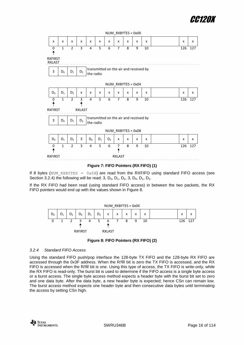
In RX mode, when the RX FIFO is empty (i.e. RXFIRST = RXLAST) the first byte received will not be
available to be read from the RXFIFO using direct FIFO access3. Please see Figure 7 (it is assumed
that the receiver uses variable packet length mode (PKT_CFG0.LENGTH_CFG = 01) and that
append status is disabled (PKT_CFG1.APPEND_STATUS = 0) for this example).
3 This byte can instead be read from extended register space (A7 – 0 = 0xDA).
CC120X
SWRU346B Page 16 of 114
0 1 2 3 4 5 6 7 8 9 10 126 127
x x
RXFIRSTRXLAST
NUM_RXBYTES = 0x00
x x x x x x xxxxx
transmitted on the air and received by the radio
3 D0 D1 D2
0 1 2 3 4 5 6 7 8 9 10 126 127
x x
RXFIRST RXLAST
NUM_RXBYTES = 0x04
x x x x x x xxD0 D1 D2
transmitted on the air and received by the radio
3 D0 D1 D2
0 1 2 3 4 5 6 7 8 9 10 126 127
x x
RXFIRST RXLAST
x x x xD0 D1 D2
NUM_RXBYTES = 0x08
3 D0 D1 D2
Figure 7: FIFO Pointers (RX FIFO) (1)
If 8 bytes (NUM_RXBYTES = 0x08) are read from the RXFIFO using standard FIFO access (see
Section 3.2.4) the following will be read: 3, D0, D1, D2, 3, D0, D1, D2.
If the RX FIFO had been read (using standard FIFO access) in between the two packets, the RX FIFO pointers would end up with the values shown in Figure 8.
0 1 2 3 4 5 6 7 8 9 10 126 127
x x
RXFIRST RXLAST
x x x xD0 D1 D2
NUM_RXBYTES = 0x04
D0 D1 D2 x
Figure 8: FIFO Pointers (RX FIFO) (2)
3.2.4 Standard FIFO Access
Using the standard FIFO push/pop interface the 128-byte TX FIFO and the 128-byte RX FIFO are accessed through the 0x3F address. When the R/W̄ bit is zero the TX FIFO is accessed, and the RX FIFO is accessed when the R/W̄ bit is one. Using this type of access, the TX FIFO is write-only, while the RX FIFO is read-only. The burst bit is used to determine if the FIFO access is a single byte access or a burst access. The single byte access method expects a header byte with the burst bit set to zero and one data byte. After the data byte, a new header byte is expected; hence CSn can remain low. The burst access method expects one header byte and then consecutive data bytes until terminating the access by setting CSn high.

CC120X
SWRU346B Page 17 of 114
If the radio tries to write to the RX FIFO after it is full or if the RX FIFO is tried read when it is empty,
the RXFIFO_OVERFLOW and RXFIFO_UNDERFLOW signals will be asserted and the radio will enter the
RX_FIFO_ERR state. Likewise, if the TX FIFO is tried written when it is full or if the TX FIFO runs
empty in the middle of a packet, the TXFIFO_OVERFLOW and TXFIFO_UNDERFLOW signals will be
asserted and the radio will enter the TX_FIFO_ERR state.
The TX FIFO may be flushed by issuing a SFTX command strobe. Similarly, a SFRX command strobe
will flush the RX FIFO. A SFTX or SFRX command strobe can only be issued in the IDLE,
TX_FIFO_ERR, or RX_FIFO_ERR states. Both FIFOs are flushed when going to the SLEEP state.
3.3 Optional PIN CTRL Radio Control Feature
The CC120X has an optional way of controlling the radio by reusing SI, SCLK, and CSn from the SPI interface. This feature allows for a simple three-pin control of the major states of the radio: SLEEP,
IDLE, RX, and TX. This optional functionality is enabled with the EXT_CTRL.PIN_CTRL_EN
configuration bit.
State changes are commanded as follows:
When CSn is high, the SI and SCLK are set to the desired state according to Table 8.
When CSn goes low, the state of SI and SCLK is latched and a command strobe is generated internally according to the pin configuration.
If the device is in the TX state and the TX command is issued, it will be ignored. For RX state, an RX command will restart RX. When CSn is low the SI and SCLK have normal SPI functionality.
All pin control command strobes are executed immediately, except the SPWD strobe. The SPWD strobe
is delayed until CSn goes high.
Pin control is useful to get precise timing on RX/TX strobes.
CSn SCLK SI Function
1 X X Chip unaffected by SCLK/SI
0 0 Generates SPWD strobe
0 1 Generates STX strobe
1 0 Generates SIDLE strobe
1 1 Generates SRX strobe
0 SPI mode
SPI mode
SPI mode (wakes up into IDLE if in SLEEP/XOFF)
Table 8: Optional Pin Control Coding
3.4 General Purpose Input/Output Control Pins
The four digital I/O pins GPIO0, GPIO1, GPIO2 and GPIO3 are general control pins configured with
IOCFGx.GPIOx_CFG (where x is 0, 1, 2, or 3). Table 10 shows the different signals that can be
monitored on the GPIO pins. The signal name field in the table should be interpreted as follows:
One signal name: The signal can be routed out to any of the four GPIO pins for full flexibility
Four signal names: The signal can only be routed out on the GPIO designated in the table.
GPIO1 is shared with the SO pin in the SPI interface. The default setting for GPIO1/SO is HIGHZ (tri-
state) output, which is useful when the SPI interface is shared with other devices. By selecting any
other of the programming options, the GPIO1/SO pin will become a generic pin when CSn is high
and function as SO when CSn is low.
When the IOCFGx.GPIOx_CFG setting is less than 0x30 and IOCFGx.GPIOx_INV is 0 (1) the
GPIO0 and GPIO2 pin will be hardwired to 0 (1), and GPIO1 and GPIO3 will be hardwired to 1 (0) in
the SLEEP state. These signals will be hardwired until the CHIP_RDYn signal goes low. If the
IOCFGx.GPIOx_CFG setting is 0x30 or higher, the GPIO pins will work as programmed also in
SLEEP state.
The GPIOs can also be used as inputs by setting IOCFGx.GPIOx_CFG = HIGHZ (48). Table 9
shows which signals can be input to the CC112X.

CC120X
SWRU346B Page 18 of 114
GPIO Pin Signal Name Signal Description
0 SERIAL_TX Serial data (TX mode). Used for both synchronous and transparent mode.
Synchronous serial mode: Data is captured on the rising edge of the serial clock
1 Reserved
2 SYNC_DETECT In blind mode (see Section 5.1.2.2) sync detection must be done by the MCU. When sync is found, the MCU should assert an output connected to this pin (GPIO2) to make the receiver switch modem parameters from sync search settings to packet receive settings similar as what is done in FIFO mode/normal mode (see for instance
AGC_CFG3.AGC_SYNC_BEHAVIOUR). SYNC_CFG0.EXT_SYNC_DETECT
must be 1
3 EXT_40K_CLOCK External 40 kHz clock signal
Table 9: GPIO Input Pin Mapping
When changing IOCFGx.GPIOx_CFG or IOCFGx.GPIOx_INV the output can be unstable and this
should be handled by the MCU by for instance disable interrupts on GPIO pins until re-configuration is done.
3.4.1 MCU Input/Interrupt
There are two main methods that can be used to generate an input/interrupt to the MCU
1. GPIO Signals
2. MCU WAKEUP
3.4.1.1 GPIO Signals
See Table 10 for the different signals that can be output from the CC120X. Note that all signals described as a pulse are two XOSC periods long.
GPIOx_CFG Signal Name Description
0 RXFIFO_THR Associated to the RX FIFO. Asserted when the RX FIFO is filled above
FIFO_CFG.FIFO_THR. De-asserted when the RX FIFO is drained below
(or is equal) to the same threshold. This signal is also available in the
MODEM_STATUS1 register
1 RXFIFO_THR_PKT Associated to the RX FIFO. Asserted when the RX FIFO is filled above
FIFO_CFG.FIFO_THR or the end of packet is reached. De-asserted
when the RX FIFO is empty
2 TXFIFO_THR Associated to the TX FIFO. Asserted when the TX FIFO is filled above
(or is equal to) (127 −FIFO_CFG.FIFO_THR). De-asserted when the TX
FIFO is drained below the same threshold. This signal is also available in
the MODEM_STATUS0 register
3 TXFIFO_THR_PKT Associated to the TX FIFO. Asserted when the TX FIFO is full. De-asserted when the TX FIFO is drained below
(127 − FIFO_CFG.FIFO_THR)
4 RXFIFO_OVERFLOW Asserted when the RX FIFO has overflowed. De-asserted when the RX FIFO is flushed (see Section 3.2.4). This signal is also available in the
MODEM_STATUS1 register
5 TXFIFO_UNDERFLOW Asserted when the TX FIFO has underflowed. De-asserted when the TX FIFO is flushed (see Section 3.2.4). This signal is also available in the
MODEM_STATUS0 register
6 PKT_SYNC_RXTX RX: Asserted when sync word has been received and de-asserted at the end of the packet. Will de-assert when the optional address and/or length check fails or the RX FIFO overflows/underflows.
TX: Asserted when sync word has been sent, and de-asserted at the end of the packet. Will de-assert if the TX FIFO underflows/overflows
7 CRC_OK Asserted simultaneously as PKT_CRC_OK. De-asserted when the first
byte is read from the RX FIFO
8 SERIAL_CLK Serial clock (RX and TX mode). Synchronous to the data in synchronous serial mode. Data is set up on the falling edge in RX and is captured on the rising edge of the serial clock in TX
9 SERIAL_RX Serial data (RX mode). Used for both synchronous and transparent mode.
Synchronous serial mode: Data is set up on the falling edge.
Transparent mode: No timing recovery (outputs just the hard limited baseband signal)

CC120X
SWRU346B Page 19 of 114
10 Reserved (used for test)
11 PQT_REACHED Preamble Quality Reached. Asserted when the quality of the preamble is above the programmed PQT value (see Section 6.8). This signal is also
available in the MODEM_STATUS1 register
12 PQT_VALID Preamble quality valid. Asserted when the PQT logic has received a sufficient number of symbols (see Section 6.8). This signal is also
available in the MODEM_STATUS1 register
13 RSSI_VALID RSSI calculation is valid
14 RSSI Signals
3 RSSI_UPDATE A pulse occurring each time the RSSI value is updated (see Figure 16)
2 RSSI_UPDATE A pulse occurring each time the RSSI value is updated (see Figure 16)
1 AGC_HOLD AGC waits for gain settling (see Figure 16)
0 AGC_UPDATE A pulse occurring each time the front end gain has been adjusted
(see Figure 16)
15 Clear channel assessment
3 CCA_STATUS Current CCA status
2 TXONCCA_DONE A pulse occurring when a decision has been made as to whether the channel is busy or not. This signal must be used as an interrupt to the
MCU. When this signal is asserted/de-asserted, TXONCCA_FAILED can
be checked
1 CCA_STATUS Current CCA status
0 TXONCCA_FAILED TX on CCA failed. This signal is also available in the MARC_STATUS0
register
16 CARRIER_SENSE_VALID CARRIER_SENSE is valid (see Figure 16)
17 CARRIER_SENSE Carrier sense. High if RSSI level is above threshold (see Section 6.9.1)
(see Figure 16)
18 DSSS signals for DSSS repeat mode (RX). MODCFG_DEV_E.MODEM_MODE = 1
3 DSSS_CLK DSSS clock (see Section 5.2.6 for more details)
2 DSSS_DATA0 DSSS data0 (see Section 5.2.6 for more details)
1 DSSS_CLK DSSS clock (see Section 5.2.6 for more details)
0 DSSS_DATA1 DSSS data1 (see Section 5.2.6 for more details)
19 PKT_CRC_OK Asserted in RX when PKT_CFG1.CRC_CFG = 1 or 10b and a good
packet is received. This signal is always on if the radio is in TX or if the
radio is in RX and PKT_CFG1.CRC_CFG = 0. The signal is de-asserted
when RX mode is entered and PKT_CFG1.CRC_CFG ≠ 0. This signal
is also available in the LQI_VAL register
20 MCU_WAKEUP MCU wake up signal. Read MARC_STATUS1.MARC_STATUS_OUT to find
the cause of the wake up event (see Section 3.4.1.2 for more details).
This signal is also available in the MARC_STATUS0 register. The signal is
a pulse
21 SYNC_LOW0_HIGH1 DualSync detect. Only valid when SYNC_CFG1.SYNC_MODE = 111b.
When SYNC_EVENT is asserted this bit can be checked to see which
sync word is found. This signal is also available in the DEM_STATUS
register
22 3 Reserved (used for test)
2 Reserved (used for test)
1 Reserved (used for test)
0 AES_COMMAND_ACTIVE Indicates that an AES command is being executed
23 LNA_PA_REG_PD Common regulator control for PA and LNA. Indicates RF operation
24 LNA_PD Control external LNA4
25 PA_PD Control external PA4
26 RX0TX1_CFG Indicates whether RF operation is in RX or TX (this signal is 0 in IDLE state)
27 Reserved (used for test)
28 IMAGE_FOUND Image detected by image rejection calibration algorithm
29 CLKEN_CFM Data clock for demodulator soft data (see Section 5.2.4 for more details)
4 This signal is active low. To control an external LNA, PA, or RX/TX switch in applications where the
SLEEP state is used it is therefore recommended to map this signal to GDO3 as this signal will be hardwired to 1(0) in the SLEEP state.

CC120X
SWRU346B Page 20 of 114
30 CFM_TX_DATA_CLK Data clock for modulator soft data (see Section 5.2.4 for more details)
31 - 32 Reserved (used for test)
33 RSSI_STEP_FOUND RSSI step found during packet reception (after the assertion of
SYNC_EVENT). The RSSI step is either 10 or 16 dB (configured through
AGC_CFG1.RSSI_STEP_THR). This signal is also available in the
DEM_STATUS register
34 3 AES_RUN AES enable. This signal is asserted as long as the AES module is
enabled given that AES.AES_ABORT = 0. This signal is also available
in the AES register
2 AES_RUN Same as 3
1 RSSI_STEP_EVENT RSSI step detected. This signal is asserted if there is an RSSI step of 3 or 6 dB during sync search or if there is an RSSI step of 10 or 16 dB during packet reception. The RSSI step is configured through
AGC_CFG1.RSSI_STEP_THR). The signal is a pulse
0 RSSI_STEP_EVENT Same as 1
35 3 Reserved (used for test)
2 Reserved (used for test)
1 LOCK Out of lock status signal. Indicates out of lock when the signal goes low.
This signal is also available in the FSCAL_CTR register
0 LOCK Same a 1
36 ANTENNA_SELECT Antenna diversity control. Can be used to control external antenna switch. If differential signal is needed, two GPIOs can be used with one
of them having IOCFGx.GPIOx_INV set to 1
37 MARC_2PIN_STATUS[1] Partial MARC state status. These signals are also available in the
MARCSTATE register
MARC_2PIN_STATUS[1] MARC_2PIN_STATUS[0] State
0 0 SETTLING
0 1 TX
1 0 IDLE
1 1 RX
38 MARC_2PIN_STATUS[0] See MARC_2PIN_STATUS[1]
39 3 Reserved (used for test)
2 TXFIFO_OVERFLOW Asserted when the TX FIFO has overflowed. De-asserted when the TX FIFO is flushed (see Section 3.2.4). This signal is also available in the
MODEM_STATUS0 register
1 Reserved (used for test)
0 RXFIFO_UNDERFLOW Asserted when the RX FIFO has underflowed. De-asserted when the RX FIFO is flushed (see Section 3.2.4). This signal is also available in the
MODEM_STATUS1 register
40 3 MAGN_VALID New CORDIC magnitude sample
2 CHFILT_VALID New channel filter sample
1 RCC_CAL_VALID RCOSC calibration has been performed at least once
0 CHFILT_STARTUP_VALID Channel filter has settled
41 3 COLLISION_FOUND Asserted if a new preamble is found and the RSSI has increased 10 or 16 dB during packet reception.
( MDMCFG1.COLLISION_DETECT_EN = 1)
This signal is also available in the DEM_STATUS register
2 SYNC_EVENT Sync word found (pulse)
1 COLLISION_FOUND Same as 3
0 COLLISION_EVENT Preamble found during receive with an RSSI step of 10 or 16 dB (pulse)
42 PA_RAMP_UP Asserted when ramping is started (for compliance testing)
43 3 CRC_FAILED Packet CRC error
2 LENGTH_FAILED Packet length error
1 ADDR_FAILED Packet address error
0 UART_FRAMING_ERROR Packet UART framing error
44 AGC_STABLE_GAIN AGC has settled to a gain. The AGC gain is reported stable whenever the current gain setting is equal to the previous gain setting. This condition is evaluated each time a new internal RSSI estimate is computed (see Figure 16)
45 AGC_UPDATE A pulse occurring each time the front end gain has been adjusted
(see Figure 16)

CC120X
SWRU346B Page 21 of 114
46 ADC data (test purposes only)
3 ADC_CLOCK ADC clock
2 ADC_Q_DATA_SAMPLE ADC sample (Q data)
1 ADC_CLOCK ADC clock
0 ADC_I_DATA_SAMPLE ADC sample (I data)
47 Reserved (used for test)
48 HIGHZ High impedance (tri-state)
49 EXT_CLOCK External clock (divided crystal clock). The division factor is controlled
through the ECG_CFG.EXT_CLOCK_FREQ register field
50 CHIP_RDYn Chip ready (XOSC is stable)
51 HW0 HW to 0 (HW to 1 achieved with IOCFGx.GPIOx_INV = 1)
52 - 53 (Reserved (used for test)
54 CLOCK_40K 40 kHz clock output from internal RC oscillator
55 WOR_EVENT0 WOR EVENT0
56 WOR_EVENT1 WOR EVENT1
57 WOR_EVENT2 WOR EVENT2
58 Reserved (used for test)
59 XOSC_STABLE XOSC is stable (has finished settling)
60 EXT_OSC_EN External oscillator enable (used to control e.g. a TCXO). Note that this signal is only asserted is a TCXO is present
61 - 63 Reserved (used for test)
Table 10: GPIO Output Pin Mapping
3.4.1.2 MCU Wake-Up
The main purpose of the MCU wake-up feature is to wake up the MCU from power down mode at the right time, i.e., when there is a need of intervention from the MCU side. To use the MCU wake-up feature one of the GPIO pins should be configured to output the
MCU_WAKEUP signal (IOCFGx.GPIOx_CFG = MCU_WAKEUP (20)). Every time this signal is asserted,
the MCU should read MARC_STATUS1.MARC_STATUS_OUT to find the cause of the wake up event
and take appropriate action.
Table 11 shows all the different cases that can initiate a MCU wake-up (assertion of MCU_WAKEUP).
Please note that MCU_WAKEUP will only be asserted when the radio enters IDLE state.

CC120X
SWRU346B Page 22 of 114
MARC_STATUS_OUT Description
00000000 No failure
00000001 RX timeout occurred. Only valid in RX mode and when not using eWOR
00000010 RX termination based on CS or PQT. Only valid in RX mode and when not using eWOR
00000011 eWOR sync lost (16 slots with no successful reception). Only valid in Feedback eWOR mode
(WOR_CFG1.WOR_MODE = 0)
00000100 Packet discarded due to maximum length filtering. Only valid in RX mode and when
RFEND_CFG0.TERM_ON_BAD_PKT is enabled.
Note: In eWOR Normal & Feedback modes the wake up pulse will not be asserted and the CC120X will go to SLEEP until the next time slot
00000101 Packet discarded due to address filtering. Only valid in RX mode and when
RFEND_CFG0.TERM_ON_BAD_PKT is enabled.
Note: In eWOR Normal & Feedback modes the wake up pulse will not be asserted and the CC120X will go to SLEEP until the next time slot
00000110 Packet discarded due to CRC filtering. Only valid in RX mode and when
RFEND_CFG0.TERM_ON_BAD_PKT is enabled.
Note: In eWOR Normal & Feedback modes the wake up pulse will not be asserted and the CC120X will go to SLEEP until the next time slot
00000111 TX FIFO overflow error occurred (the MCU should flush the TX FIFO)
00001000 TX FIFO underflow error occurred (the MCU should flush the TX FIFO)
00001001 RX FIFO overflow error occurred (the MCU should flush the RX FIFO)
00001010 RX FIFO underflow error occurred (the MCU should flush the RX FIFO)
00001011 TX ON CCA failed. A TX strobe was ignored due to a busy channel. In parallel the TXONCCA_DONE
signal is asserted together with the TXONCCA_FAILED signal. These signals can be output on GDO2
and GDO0 respectively by setting IOCFG2/0.GPIO2/0_CFG = 15. The TXONCCA_FAILED signal
is also available in the MARC_STATUS0 register together with TXONCCA_DONE
01000000 TX finished successfully (the CC120X is ready for the next operation)
10000000 RX finished successfully (a packet is in the RX FIFO ready to be read)
Table 11: MARC_STATUS_OUT
By setting RFEND_CFG0.CAL_END_WAKE_UP_EN = 1, the MCU will be given additional wake up
pulses at the end of calibration (MARC_STATUS_OUT will be 0).
4 On-Chip Temperature Sensor
The CC120X has a temperature sensor that can be activated by using the register settings shown in Table 12. The temperature sensor is based on a PTAT current from a band-gap cell fed to a resistor to generate a PTAT voltage.Please see DN403 [4] for more details.
Register Value
IOCFG1 0x80
ATEST 0x2A
ATEST_MODE 0x0C
GBIAS1 0x07
Table 12: Register Settings for Activating the Temp Sensor

CC120X
SWRU346B Page 23 of 114
5 Common Receive and Transmit Configurations
5.1 Data Communication Modes
The CC120X supports different ways of setting up data communication, each with a defined area of use. The following sections contain a description of the high level functionality of these different modes of operation.
5.1.1 FIFO Mode/Normal Mode
FIFO mode is the preferred mode of operation. In this mode data is read from the RX FIFO and written to the TX FIFO, making the data transfer to/from the MCU less time critical compared to what is the case in the other modes. Using the FIFOs to buffer data allows the MCU to be in sleep mode during RX/TX, reducing system power consumption.
In FIFO mode, sync and preamble insertion/detection are done automatically, and several other optional packet handling features are supported in this mode. FIFO mode/Normal mode is enabled by
setting PKT_CFG2.PKT_FORMAT = 0.
5.1.2 Synchronous Serial Mode
In synchronous serial mode, data is clocked in and out of the CC112X by a clock provided by the device. More details on this mode are found in Section 8.9.1. Synchronous serial mode is enabled by
setting PKT_CFG2.PKT_FORMAT = 1.
5.1.2.1 Sync Insertion/Detection Enabled
After the sync word is received/transmitted (SYNC_CFG1.SYNC_MODE ≠ 0), data is clocked in/out on
a GPIO pin with the associated clock on another GPIO pin. The serial clock is not output from the device before the sync word is sent/received, hence the MCU can be in sleep mode until sync is detected in RX mode.
Synchronous serial mode makes use of the WaveMatch detector, which means the performance will be similar to the performance in FIFO mode.
5.1.2.2 Sync Insertion/Detection Disabled (Blind Mode)
Blind mode is synchronous serial mode with SYNC_CFG1.SYNC_MODE = 0. In this mode, the CC120X
will demodulate data/noise and it is the MCU that needs to monitor the data stream to find the framing information. The serial clock will run continuously when the radio is in active mode.
If framing information is present in the signal, it is strongly advised to use either FIFO mode or synchronous serial mode with sync detection enabled to make use of the strong WaveMatch detector
in CC120X (see Section 6.6).
Blind mode can be used in applications with no framing information, e.g. streaming data applications.
5.1.3 Transparent Serial Mode
In transparent serial mode (PKT_CFG2.PKT_FORMAT = 11b) the CC120X is configured to resemble a
legacy analog RF front end device. In this mode data is only filtered through the channel filter and the hard limited baseband signal is output directly on a GPIO pin. No symbol rate recovery or bit timing is performed by the radio.
Transparent mode can be used for applications that have packet formats incompatible with the built-in demodulator. Examples are pulse width modulation and pulse position modulation. When using transparent mode, the demodulation must be performed by the MCU.
More details on this mode are found in Section 8.9.2.

CC120X
SWRU346B Page 24 of 114
5.2 Modulation Formats
CC120X supports amplitude and frequency shift modulation formats. The desired modulation format is
set in the MODCFG_DEV_E.MOD_FORMAT register.
Optionally, the data stream can be Manchester encoded by the modulator and decoded by the
demodulator. This option is enabled by setting MDMCFG1.MANCHESTER_EN = 1. Note that
Manchester encoding/decoding is only performed on the payload (including optional length and address field) and the CRC and that all packet handling features are still available. In applications where preamble and sync word also need to be Manchester encoded, this can be achieved by
selecting PREAMBLE_CFG1.PREAMBLE_WORD = 10b or 11b and manually encoding a two byte long
sync word and write it to SYNC3/2/1/0.
5.2.1 Frequency Shift Keying
CC120X supports both 2-FSK and 4-FSK modulation. Both can optionally be shaped by a Gaussian filter with BT = 0.5, producing a GFSK modulated signal. This spectrum-shaping feature improves adjacent channel power (ACP) and occupied bandwidth. When selecting 4-(G)FSK, the preamble and sync word is sent using 2-(G)FSK (see Figure 9).
+1
+1/3
-1/3
-11 0 1 0 1 0 1 0 1 1 0 1 0 0 1 1 00 01 01 11 10 00 11 01
Preamble0xAA
Sync0xD3
Data0x17 0x8D
1/Symbol Rate 1/Symbol Rate 1/Symbol Rate
Figure 9: Data Sent Over the Air (MDMCFG2.SYMBOL_MAP_CFG = 0)
In ‘true’ 2-FSK systems with abrupt frequency shifting, the spectrum is inherently broad. By making the frequency shift ‘softer’, the spectrum can be made significantly narrower. Thus, higher symbol rates can be transmitted in the same bandwidth using GFSK.
When 2-(G)FSK/4-(G)FSK modulation is used, the DEVIATION_M and MODCFG_DEV_E.DEV_E
register specifies the expected frequency deviation of incoming signals in RX and should be the same as the TX deviation for demodulation to be performed reliably and robustly.
The frequency deviation is programmed with the DEV_M and DEV_E values in the DEVIATION_M and
MODCFG_DEV_E.DEV_E register. The value has an exponent/mantissa form, and the resultant
deviation is given by Equation 1 and Equation 2.
[Hz]2)_256(2
_
22
EDEVxoscdev MDEV
ff
Equation 1: fdev (DEVIATION_E > 0)
[Hz] _221
MDEVf
f xoscdev
Equation 2: fdev (DEVIATION_E = 0)

CC120X
SWRU346B Page 25 of 114
The symbol encoding can be configured through the MDMCFG2.SYMBOL_MAP_CFG register field as
shown in Table 135 (SYMBOL_MAP_CFG = 0 by default).
Format Symbol Coding
SYMBOL_MAP_CFG
= 00b SYMBOL_MAP_CFG
= 01b SYMBOL_MAP_CFG
= 10b SYMBOL_MAP_CFG =
11b
2-(G)FSK
OOK/ASK
‘0’ −Deviation [AMin] +Deviation [AMax] +Deviation[AMax] +Deviation [AMax]
‘1’ +Deviation [AMax] −Deviation [AMin] −Deviation [AMin] −Deviation [AMin]
4-(G)FSK ‘00’ −Deviation /3 −Deviation +Deviation /3 +Deviation
‘01’ −Deviation −Deviation /3 +Deviation +Deviation /3
‘10’ +Deviation /3 +Deviation −Deviation /3 −Deviation
‘11’ +Deviation +Deviation /3 −Deviation −Deviation /3
Table 13: Symbol Encoding for 2-(G)FSK and 4-(G)FSK Modulation
5.2.2 Amplitude Modulation (ASK) and on-off keying (OOK)
CC120X supports two different forms of amplitude modulation: On-Off Keying (OOK) and Amplitude Shift Keying (ASK).
OOK modulation simply turns the PA on or off to modulate ones and zeros respectively.
When using OOK/ASK bit shaping can be enabled and the CC120X allows programming of both the shape length and of the modulation depth (the difference between 1 and 0). Pulse shaping produces a more bandwidth constrained output spectrum (see Figure 10).
The shape length is configured through PA_CFG0.RAMP_SHAPE and the modulation depth is
configured through ASK_CFG.ASK_DEPTH.
Figure 10: OOK with Shaping
5 AMin = Minimum Amplitude and AMax = Maximum Amplitude when OOK/ASK is used

CC120X
SWRU346B Page 26 of 114
5.2.3 Minimum Shift Keying
When using MSK6, the complete transmission (preamble, sync word, and payload) will be MSK
modulated.
MSK modulation is configured by MODCFG_DEV_E.MOD_FORMAT set to 2-(G)FSK modulation and
frequency deviation set to ¼ of symbol rate. Then phase shifts are performed with a constant transition time. Table 14 shows what the frequency deviation should be programmed to for different symbol rates to achieve a modulation index ~0.5.
Symbol Rate [ksps] Frequency Deviation [kHz] Actual Modulation Index
1.0 0.25 0.4940
1.2 0.3 0.5083
2.4 0.6 0.5083
4.8 1.2 0.5004
9.6 2.4 0.5006
19.6 4.8 0.5001
38.4 9.6 0.5007
50 12.5 0.5005
76.8 19.2 0.4997
100 25.0 0.5005
125 31.25 0.5005
250 62.5 0.5005
500 125 0.5005
Table 14: MSK Parameters
5.2.4 Custom Frequency Modulation(CFM)/Analog FM
CC120X supports a simple scheme to do custom frequency modulation/analog FM (e.g. communication with analog legacy voice devices, N-FSK systems). This feature utilizes the high resolution PLL and lets the user in a simple way directly control/read the instantaneous frequency without SPI overhead.
Custom frequency modulation is enabled by setting MDMCFG2.CFM_DATA_EN = 1.
One register (CFM_TX_DATA_IN) is used to set the carrier frequency offset and another register
(CFM_RX_DATA_OUT) is used to read the instantaneous frequency offset. The two registers have the
same format (two’s complement) to simplify SW control in both TX and RX. Accessing these registers
should be done using burst mode combined with setting EXT_CTRL.BURST_ADDR_INCR_EN = 0 to
continuously access the same address without any SPI address overhead.
The signal CFM_TX_DATA_CLK can be output on a GPIO by setting IOCFGx.GPIOx_CFG = 30. This
signal will be asserted every time the CFM_TX_DATA_IN register should be written and should be
used as an interrupt to the MCU to synchronize the SPI data to the internal modulation rate. The signal runs at 16x the programmed symbol rate.
The signal CLKEN_CFM should be output on a GPIO (IOCFGx.GPIOx_CFG = 29) and used as a
trigger to read the CFM_RX_DATA_OUT samples. This signal runs at the same rate as the
programmed symbol rate.
Note that in TX mode, 3 dummy symbols should be written to the CFM_TX_DATA_IN register before
strobing SIDLE in order for all symbols to be sent on the air before TX mode is ended.
6 Identical to offset QPSK with half-sine shaping (data coding may differ).

CC120X
SWRU346B Page 27 of 114
When using custom frequency modulation there are 129 values (referred to as fOFFSET) between −fdev and +fdev that can be used (see Equation 1 and Equation 2 in Section 5.2.1 for details on how to program the frequency deviation). fOFFSET is given by Equation 3.
[Hz] 64
___ INDATATXCFMff devOFFSET
Equation 3: fOFFSET7
The modulator writes values to the PLL at 16x the programmed symbol rate. Between the modulator
and the PLL there is an optional linear upsampler configured through the MDMCFG2.UPSAMPLER_P
register field.
5.2.5 DSSS PN Mode
CC120X supports DSSS PN mode for applications requiring high sensitivity. Preamble and sync word is unchanged, but the payload data bit is spread with a fixed PN gold sequence initialized at the beginning of each packet. The spreading factor is set to 4 hence the effective data rate is reduced by a factor 4. The PN gold sequence is generated from a combination of two 7-bits LFSR registers with generator polynomial given by Equation 4 and Equation 5. h1(p) is initialized to 0x04 and h2(p) is initialized to 0x0B.
1)(1 237 ppppph
Equation 4: h1(p)
1)(2 37 ppph
Equation 5: h2(p)
The resulting bit is then XOR’ed with the transmitted bits, where each of the input data bits is mapped into 4 consecutive symbols, as shown in the following Figure 11. The figure shows what is sent on the air when the input data is 101b.
+
+ + +
+ +
Input Data @ ¼ Symbol Rate
GoldSequence
TX Data @ Symbol Rate
Gold Sequence
Input Data @ ¼ Symbol Rate
TX Data @ Symbol Rate
Bit n Bit n + 2Bit n + 1
Figure 11: Gold Sequence Generation
The resulting sequence has good autocorrelation properties.
7 This equation is only valid when -64 ≤ CFM_TX_DATA_IN ≤ +64. CFM_TX_DATA_IN > 64
corresponds to +fdev while CFM_TX_DATA_IN < -64 gives a frequency of −fdev. CFM_TX_DATA_IN
= -128 is the same as setting CFM_TX_DATA_IN = 0.

CC120X
SWRU346B Page 28 of 114
At the receiver, the PN gold sequence is known and is initialized at the beginning of each packet. For every group of 4 incoming symbols, two accumulated distance computation are performed; one assuming that a ‘0’ was sent and the other assuming that a ‘1’ was sent, and the most likely transmitted bit is chosen.
DSSS PN mode is enabled by setting MODCFG_DEV_E.MODEM_MODE = 10b8.
When using this mode both FIFO mode and synchronous serial mode are supported
(PKT_CFG2.PKT_FORMAT = 0 or 1).
5.2.6 DSSS Repeat Mode
CC120X supports DSSS repeat mode for applications requiring high sensitivity. In DSSS repeat mode, preamble is unchanged. The payload data bits are spread using the sync word meaning that the complete sync word is sent for every 1 in the payload and the inverted sync word is sent for every 0 in
the payload. Only SYNC_CFG1.SYNC_MODE = 1 and 010b are supported (11 or 16 bits).
DSSS repeat mode is enabled by setting MODCFG_DEV_E.MODEM_MODE = 18.
In TX mode all packet handling features are supported, but the packet format must be set to FIFO
mode (PKT_CFG2.PKT_FORMAT = 0).
In RX mode, none of the packet handling features are supported and synchronous serial mode must
be selected (PKT_CFG2.PKT_FORMAT = 1, MDMCFG1.FIFO_EN = 0 and
MDMCFG0.TRANSPARENT_MODE_EN = 0). It is the MCU’s responsibility to extract the demodulated
data, which are available on GPIO by configuring IOCFGx.GPIOx_CFG = 18 (GPIO3/1 =
DSSS_CLK, GPIO2 = DSSS_DATA0 and GPIO0 = DSSS_DATA1). The clock (DSSS_CLK) will run at a
frequency twice the programmed symbol rate and will start as soon as the radio enters RX state.
The receiver uses two correlation filters (see Section 6.7 for more details) to search for sync word and
inverted sync word. Each output is connected directly to DSSS_DATA1 and DSSS_DATA0. After
strobing RX the sync search starts, and when a sync word or inverted sync word is detected the corresponding serial data line will be asserted high, otherwise the data line is low. The output from the correlation filter is high as long as the sync word/inverted sync word is detected, so the MCU needs to do edge detect on the data in order to not duplicate the demodulated data bit. Figure 12 shows how the DSSS signal will look like on the GPIO pins when the following packet is sent on the air using DSSS repeat mode: 0x03, 0x55, 0x55, 0x55. Symbol rate is 1.2 ksps.
Figure 12: DSSS Repeat Mode
8 DSSS PN mode and DSSS repeat mode are not supported for 4’ary modulation formats.
Note. Assertion of DSSS_DATA1 and DSSS_DATA0 within the first 5 DSSS_CLK edges after
entering RX should be ignored.

CC120X
SWRU346B Page 29 of 114
5.3 Forward Error Correction
FEC is enabled by settings PKT_CFG1.FEC_EN = 1. The FEC implemented in CC120X is compatible
with the 802.15.4g FEC (NRNSC coding) when PKT_CFG2.FS_MODE_EN = 1 and the FEC
implemented in the CC1101 when PKT_CFG2.FS_MODE_EN = 0.
The RXFIFO must not be accessed during packet reception when FEC is enabled, hence the complete packet, excluding preamble and sync, must not be larger than 128 bytes. When using FEC, the symbol rate must not exceed 250 ksps for 4’ary modulation formats or 500 ksps for 2’ary modulation formats.
5.4 Symbol Rate Programming
The symbol rate used in transmit and the symbol rate expected in receive is programmed by the
SYMBOL_RATE_M and the SYMBOL_RATE_E configuration settings. The symbol rate, RSYMBOL, is given
by Equation 6 and Equation 7 and is in ksps. Note that SYMBOL_RATE_M is 20 bits wide and consists
of the register fields SRATE_M_19_16, SRATE_M_15_8 and SRATE_M_7_0 found in SYMBOL_RATE2,
SYMBOL_RATE1, and SYMBOL_RATE0 respectively.
[ksps] 2
2)_2(39
_20
XOSC
ESRATE
Symbol fMSRATE
R
Equation 6: Symbol Rate (SRATE_E > 0)
[ksps] 2
_38 XOSCSymbol f
MSRATER
Equation 7: Symbol Rate (SRATE_E = 0)
Equation 8 and Equation 9 can be used to find suitable register values for a given symbol rate.
202
log_
39
2
XOSC
Symbol
f
RESRATE
Equation 8: SRATE_E
20
_
39
22
2_
ESRATE
XOSC
Symbol
f
RMSRATE
Equation 9: SRATE_M
If SYMBOL_RATE_M is rounded to the nearest integer and becomes 220
, one should increment
SYMBOL_RATE_E and use SYMBOL_RATE_M = 0 instead.
The symbol rate can be set up to 500 ksps with the minimum step size according to Table 15.

CC120X
SWRU346B Page 30 of 114
Min Symbol Rate [ksps] Typical Symbol Rate [ksps] Max Symbol Rate [ksps] Symbol Rate Step Size [ksps]
0 0.04 0.15 0.00000014
0.15 0.25 0.3 0.00000014
0.61 1.2 1.22 0.0000006
1.22 2.4 2.44 0.000001
2.44 4.8 4.88 0.000002
4.88 9.6 9.76 0.000005
19.5 25 39.0 0.000018
39.0 50 78.1 0.000037
78.1 100 125 0.000074
156 250 312 0.00015
312 500 500 0.00029
Table 15: Symbol Rate Step Size
Note that for 4-(G)FSK, DSSS mode, Manchester mode, and FEC, the data rate and symbol rate is not equal. Table 16 shows the relationship between data rate and symbol rate.
Modulation Format / Data Encoding Data Rate/Symbol Rate Ratio
2-(G)FSK/OOK/ASK 1
Symbol
Bit
R
R
Manchester Mode 2
1
Symbol
Bit
R
R
4-(G)FSK 2
Symbol
Bit
R
R
DSSS Mode
Factor Spreading
1
Symbol
Bit
R
R
FEC 2
1
Symbol
Bit
R
R
Table 16: Data Rate vs. Symbol Rate
6 Receive Configuration
6.1 RX Filter Bandwidth
In order to meet different channel width requirements, the RX filter BW is programmable. The
CHAN_BW.ADC_CIC_DECFACT and CHAN_BW.BB_CIC_DECFACT register fields control the RX filter
BW together with the crystal oscillator frequency. It is recommended to use SmartRF Studio [1] to generate settings for a given RX filter BW.
Equation 10 gives the relation between the register settings and the RX filter bandwidth.
BB_CIC_DECFACT is found in CHAN_BW.
[Hz] 2__Factor Decimation
BWFilter RXDECFACTCICBB
fxosc
Equation 10: RX Filter BW

CC120X
SWRU346B Page 31 of 114
The decimation factor is 12, 24, or 48 depending on the CHAN_BW.ADC_CIC_DECFACT setting.
Table 17 lists the RX filter bandwidth configurations supported by the CC120X. The RX filter BW should
never be set higher than 1666.7 kHz. Note that values marked ( ) are only available on CC1200.
As a rule of thumb, one should set the decimation factor as high as possible for a given RX filter BW,
meaning that the preferred setting for 208.3 kHz is ADC_CIC_DECFACT = 2 and
BB_CIC_DECFACT = 2.
BB_CIC_DECFACT Decimation Factor BB_CIC_DECFACT Decimation Factor
12 24 48 12 24 48
1 1666.7 833.3 416.7 23 72.5 36.2 18.1
2 833.3 416.7 208.3 24 69.4 34.7 17.4
3 555.6 277.8 138.9 25 66.7 33.3 16.7
4 416.7 208.3 104.2 26 64.1 32.1 16.0
5 333.3 166.7 83.3 27 61.7 30.9 15.4
6 277.8 138.9 69.4 28 59.5 29.8 14.9
7 238.1 119.0 59.5 29 57.5 28.7 14.4
8 208.3 104.2 52.1 30 55.6 27.8 13.9
9 185.2 92.6 46.3 31 53.8 26.9 13.4
10 166.7 83.3 41.7 32 52.1 26.0 13.0
11 151.5 75.8 37.9 33 50.5 25.3 12.6
12 138.9 69.4 34.7 34 49.0 24.5 12.3
13 128.2 64.1 32.1 35 47.6 23.8 11.9
14 119.0 59.5 29.8 36 46.3 23.1 11.6
15 111.1 55.6 27.8 37 45.0 22.5 11.3
16 104.2 52.1 26.0 38 43.9 21.9 11.0
17 98.0 49.0 24.5 39 42.7 21.4 10.7
18 92.6 46.3 23.1 40 41.7 20.8 10.4
19 87.7 43.9 21.9 41 40.7 20.3 10.2
20 83.3 41.7 20.8 42 39.7 19.8 9.9
21 79.4 39.7 19.8 43 38.8 19.4 9.7
22 75.8 37.9 18.9 44 37.9 18.9 9.5
Table 17: RX Filter BW in kHz
By compensating for a frequency offset between the transmitter and the receiver, the filter bandwidth can be reduced and the sensitivity can be improved.
The following rule should be used when programming the RX filter BW:
SYNC_CFG0.RX_CONFIG_LIMITATION = 0:
o The RX filter BW must be larger or equal to twice the symbol rate
SYNC_CFG0.RX_CONFIG_LIMITATION = 1:
o The RX filter BW must be larger or equal to the symbol rate
A narrow bandwidth gives better sensitivity and selectivity at the cost of more accurate RF crystals.
The CHAN_BW.ADC_CIC_DECFACT sets the bandwidth into the digital low-IF mixer.
If the selected RX filter bandwidth is large compared to the symbol rate (10 times of more), sensitivity
can be improved by setting MDMCFG0.DATA_FILTER_EN = 1.
6.2 DC Offset Removal
CC120X supports Low-IF and Zero-IF receiver architecture, which is set by the
IF_MIX_CFG.CMIX_CFG register field. For more information see section 9.12. For Zero-IF the DC
offset removal must be enabled by setting DCFILT_CFG.DCFILT_FREEZE_COEFF = 0. The
DCFILT_CFG configures the DC filter bandwidth, both during settling period and during tracking.
There is a tradeoff between bandwidth and settle time. Narrower DC filter bandwidth requires longer settling time, but improves performance.
For best performance, use Low-IF receiver architecture when possible.

CC120X
SWRU346B Page 32 of 114
6.3 Feedback to PLL
Register FREQOFF_CFG enables feedback to the PLL to "increase the RX filter BW". The noise
bandwidth, and hence sensitivity, will not increase when enabling this feature. Setting FREQOFF_CFG
to 0x30 and 0x34 enables feedback to the PLL and increases bandwidth from "programmed RX filter BW" to "programmed RX filter BW ± RX filter BW/4" and "programmed RX filter BW ± RX filter BW/8"
respectively. As an example, RX filter BW is programmed to 33.3 kHz and FREQOFF_CFG = 0x30,
the feedback to PLL increases this filter to 50 kHz (although 33.3 kHz is still the noise bandwidth).
Figure 13 shows two plots of PER vs. input power level vs. frequency offset. In the first plot the RX
filter BW is programmed to 50 kHz and FREQOFF_CFG = 0x22 (i.e. feedback to PLL disabled). In
the second plot the RX filter BW is programmed to 33.3 kHz and FREQOFF_CFG = 0x30 (i.e.
feedback to PLL enabled). It is evident from the plots that the noise bandwidth is lower in the second plot without the need to use a tighter tolerance crystal.
Figure 13: Feedback to PLL
50 kHz
No feedback
to PLL
33.3 kHz and feedback
to PLL

CC120X
SWRU346B Page 33 of 114
6.4 Automatic Gain Control
CC120X contains an Automatic Gain Control (AGC) for adjusting the input signal level to the demodulator.
The AGC behavior depends on the following register fields:
AGC_CFG2.FE_PERFORMANCE_MODE
o Sets the correct gain tables to be applied for a given operation mode (See Table 18). See the complete register description for what the different modes are.
~39 dB Index 0 ~27 dB Index 0 ~39 dB Index 0
~36 dB Index 1 ~24 dB Index 1 ~32 dB Index 1
~32 dB Index 2 ~21 dB Index 2 ~27 dB Index 2
~29 dB ~18 dB ~21 dB
~27 dB ~15 dB ~15 dB
~24 dB ~12 dB ~9 dB
~21 dB ~9 dB ~3 dB
~18 dB ~6 dB ~0 dB Index 7
~15 dB ~3 dB
~12 dB ~0 dB
~9 dB ~-6 dB
~6 dB ~-12 dB
~3 dB ~-18 dB
~0 dB ~-21 dB Index 13
~-6 dB
~-12 dB
~-18 dB
~-21 dB Index 17
FE_PERFORMANCE_MODE
= 0 or 1
FE_PERFORMANCE_MODE
= 10b
FE_PERFORMANCE_MODE
= 11b
Table 18: AGC Gain Tables
o The AGC_CFG2.AGC_MAX_GAIN and AGC_CFG3.AGC_MIN_GAIN register fields are used
to set the table indexes for maximum and minimum gain respectively. For example, setting
AGC_MAX_GAIN = 2 and AGC_MIN_GAIN = 15 limits the gain table to 14 entries, where
max gain is ~32 dB and min gain is ~-12 dB. A lower maximum gain will reduce power consumption in the receiver front end, since the highest gain settings are avoided. Limiting max gain also improves worst case linearity in the front-end, something that is very useful when using external LNA.
AGC_REF.AGC_REFERENCE
o Sets the reference value for the AGC. The reference value is a compromise between blocker tolerance/selectivity and sensitivity. The AGC reference level must be higher than the minimum SNR to the demodulator. The AGC reduces the analog front end gain when the magnitude output from the channel filter is greater than the AGC reference level. An optimum AGC reference level is given by several conditions, but a rule of thumb is given by Equation 11.
TRSSI_OFFSE92)BW FILTER RX(log10NCEAGC_REFERE 10
Equation 11: AGC Reference9
9 For Zero-IF configuration, AGC hysteresis > 3 dB, or modem format which needs SNR > 15 dB a
higher AGC reference value is needed

CC120X
SWRU346B Page 34 of 114
AGC_CFG3.AGC_SYNC_BEHAVIOR
o Sets the AGC behavior and RSSI update behavior after a sync word is found
AGC_CFG1.AGC_WIN_SIZE
o Sets the AGC integration window size for each value. Samples refer to the RX filter sampling frequency, which is 4 times the programmed RX filter BW
AGC_CFG1.AGC_SETTLE_WAIT
o Sets the wait time between AGC gain adjustments
AGC_CFG2.AGC_MAX_GAIN
o Sets the maximum gain
AGC_CFG3.AGC_MIN_GAIN
o Sets the minimum gain
See Figure 16 for detailed timing information on different AGC signals.
6.5 Image Compensation
CC120X has support for the ImageExtinct image compensation algorithm that digitally compensates for I/Q mismatch. ImageExtinct removes the image component, removing any issues at the system image frequency. ImageExtinct removes the need for time consuming image calibration steps in system production test, reducing both test time and test cost. This feature is enabled by setting
IQIC.IQIC_EN = 1. When this feature is enabled, fIF > RX filter BW. Figure 14 shows selectivity
versus frequency with IQ image compensation enabled and disabled.
Figure 14: IQIC Enabled/Disabled (image at −206 kHz offset)
0
10
20
30
40
50
60
70
86
7.8
86
7.9
86
8,0
00
0
86
8.0
5
86
8.0
94
86
8.1
86
8.1
5
86
8.1
97
86
8.2
86
8.2
25
86
8.2
5
86
8.2
75
86
8.2
88
86
8.3
Sele
ctiv
ity
Re
lati
ve [
dM
]
Frequency [MHz]
IQ Enabled
IQ Disabled

CC120X
SWRU346B Page 35 of 114
6.6 Bit Synchronization
The bit synchronization algorithm extracts the clock from the incoming symbols. The algorithm requires that the expected symbol rate is programmed as described in Section 5.3. Re-synchronization is performed continuously to adjust for any offset between the incoming and programmed symbol rate.
It is possible to select between two different bit synchronization algorithms.
TOC_CFG.TOC_LIMIT sets the bit synchronization algorithm and Table 19 below shows the
properties of the bit synchronization algorithms.
TOC_LIMIT Symbol Rate Offset Tolerance Required Preamble Length
0 < 0.2 % 0.5 byte (only for gain adjustment)
1 < 2 % 2 - 4 bytes
2 Reserved
3 < 12 % 2 - 4 bytes
Table 19: Bit Synchronization Property
Using the low tolerance setting (TOC_LIMIT = 0) greatly reduces system settling times and system
power consumption as no preamble bits are needed for bit synchronization or frequency offset compensation (4 bits preamble needed for AGC settling).
6.7 Byte Synchronization, Sync Word Detection
Byte synchronization is achieved by a continuous sync word search using the novel WaveMatch
capture logic (correlation filter). The sync word is configured through the SYNC3/2/1/0 registers and
can be programmed to be 11, 16, 18, 24 or 32 bits. This is done through the
SYNC_CFG1.SYNC_MODE register field. In TX mode, these bits are automatically inserted at the start
of the packet by the modulator. The MSB in the sync word is sent first. In RX mode, the demodulator uses the sync word to find the start of the incoming packet.
The CC120X will continuously calculate a sync word qualifier value to distinguish the sync word from
background noise. This value is available in the PQT_SYNC_ERR.SYNC_ERROR register field. If the
sync word qualifier value is less than the programmed sync threshold (SYNC_CFG1.SYNC_THR)
divided by 2 the demodulator starts to demodulate the packet.
The CC120X supports DualSync search which makes it possible to concurrently search for 2 different
16 bit sync words. DualSync search is enabled by settings SYNC_CFG1.SYNC_MODE = 111b. As
soon as one of the sync words is found, the RX FIFO starts to fill up.
In addition to continuously calculating a sync word qualifier value the CC120X has several other features that can be used to decrease the likelihood of detecting “false” packets.
Strict Sync Word Bit Check
This feature is enabled through SYNC_CFG0.STRICT_SYNC_CHECK and allows for additional
bit check on sync word. This feature is especially useful if the sync word used has weak correlation properties. There are three levels of the strict sync check, where level 3 is the setting that allows for the least amount of error in the sync word (the strictest setting). Setting
STRICT_SYNC_CHECK = 11b disables this feature and is the settings that will give the best
sensitivity.
Carrier Sense Gating
When MDMCFG1.CARRIER_SENSE_GATE = 1, the demodulator will not start to look for a sync
word before CARRIER_SENSE is asserted. See Section 6.9.1 for more details on CS.
PQT Gating
When SYNC_CFG0.PQT_GATING_EN = 1, the demodulator will not start to look for a sync
word before a preamble is detected. The preamble detector must be enabled for this feature to
work (PREAMBLE_CFG0.PQT_EN = 1). See Section 6.8 for more details on PQT.

CC120X
SWRU346B Page 36 of 114
6.8 Preamble Detection
CC120X has a high performance preamble detector which can be turned on by setting
PREAMBLE_CFG0.PQT_EN = 1.
The preamble quality estimator uses an 8 bits wide correlation filter to find a valid preamble. A
preamble qualifier value is available through the PQT_SYNC_ERR.PQT_ERROR register field while the
threshold is configured with the register field PREAMBLE_CFG0.PQT.
A preamble is detected if the preamble qualifier value is less than the programmed PQT threshold. A “Preamble Quality Reached” signal can be observed on one of the GPIO pins by setting
IOCFGx.GPIOx_CFG = PQT_REACHED (11). It is also possible to determine if preamble quality is
reached by checking the PQT_REACHED bit in the MODEM_STATUS1 register. The PQT_REACHED
signal will stay asserted as long as a preamble is present but will de-assert on sync found. If the preamble disappears, the signal will de-assert after a timeout defined by the sync word length + 10
symbols after preamble was lost. When SYNC_CFG0.PQT_GATING_EN = 1, sync word search is
only gated if a preamble is detected.
The PQT can also be used as a qualifier for the optional RX termination timer (see Section 9.5.1 for more details).
A PQT startup timer is available and programmable through the
PREAMBLE_CFG0.PQT_VALID_TIMEOUT register. The PQT response time is the time it takes from
entering RX mode until PQT_VALID is asserted. The PQT response time is given by Equation 12,
where T0 is given by Equation 18 and T1 is given by Equation 13 or Equation 14 depending on the
SYMBOL_RATE2.SRATE_E setting. BB_CIC_DECFACT is found in register CHAN_BW and the
decimation factor is 12, 24, or 48, given by the CHAN_BW.ADC_CIC_DECFACT register field. SRATE_E
and SRATE_M are found in the SYMBOL_RATEn registers (where n = 0, 1, 2) and
RX_CONFIG_LIMITATION is found in SYNC_CFG0. In Equation 13 or Equation 14, x = Decimation
Factor·BB_CIC_DECFACT.
10Time Response PQT TT
Equation 12: PQT Response Time
XOSCfLIMITATIONCONFIGRX
xMSRATE
LIMITATIONCONFIGRXFLOOR
T1
562__.2
1_
)2__2(Timer Startup PQT2x
1
38
Equation 13: T1 when SRATE_E = 0
XOSC
ESRATE
fLIMITATIONCONFIGRX
xMSRATE
LIMITATIONCONFIGRXFLOOR
T1
562__.2
)2_(
)2__2(Timer Startup PQT2x
1
_20
39
Equation 14: T1 when SRATE_E ≠ 0
The different PQT startup timer values enables a tradeoff between speed and accuracy as preamble
search will not be gated before PQT_VALID is asserted. PQT_VALID can be monitored on a GPIO pin
by setting IOCFGx.GPIOx_CFG = PQT_VALID (12).

CC120X
SWRU346B Page 37 of 114
6.9 RSSI
The AGC module returns an estimate on the signal strength received at the antenna called RSSI (Received Signal Strength Indicator). The RSSI is a 12 bits two's complement number with 0.0625 dB resolution hence ranging from –128 to 127 dBm. A value of –128 dBm indicates that the RSSI is
invalid. The RSSI can be found by reading RSSI1.RSSI_11_4 and RSSI0.RSSI_3_0. It should be
noted that for most applications using the 8 MSB bits of the RSSI, with 1 dB resolution, is good enough.
To get a correct RSSI value a calibrated RSSI offset value should be added to the value given by
RSSI[11:0] (the RSSI offset will be a negative number). The RSSI offset value can be found by
input a signal of known strength to the radio when AGC_GAIN_ADJUST.GAIN_ADJUSTMENT is
0x0010
.
The RSSI value is output from a configurable moving average filter in order to reduce uncertainty in the RSSI estimates. It is as such possible to trade RSSI computation speed/update rate against RSSI
accuracy. This trade-off is determined by configuring the AGC_CFG0.RSSI_VALID_CNT register. This
register field gives the number of new input samples to the moving average filter (internal RSSI
estimates) that are required before the next update of the RSSI value11
. The RSSI_VALID signal will
be asserted from the first RSSI update. RSSI_VALID is available on a GPIO by setting
IOCFGx.GPIOx_CFG = RSSI_VALID (13) or can be read from the RSSI0 register.
Carrier Sense (CS) indication will also be affected by the setting of AGC_CFG0.RSSI_VALID_CNT.
After the RSSI is valid it will be continuously compared to the CS threshold set in the AGC_CS_THR
register, but since the RSSI update rate is given by the RSSI_VALID_CNT register field, this will in
practice limit the CS update rate as well. The exception is when the CS threshold is changed while in
RX mode. The CARRIER_SENSE signal will then be updated immediately (if needed). For more info
on CS, see Section 6.9.1. Figure 15 shows when CS is updated with respect to the RSSI.
Signal Strength
Time
RSSI Update
CS Threshold
RSSI
CARRIER_SENSE
Figure 15: CS vs. RSSI_UPDATE
Figure 16 shows an example of the behavior of RSSI specific signals given two different values for the
AGC_CFG0.RSSI_VALID_CNT register value (1 and 10b).
10 The RSSI offset changes if MDMCFG1.DVGA_GAIN is changed
11 By setting the IOCFG3.GPIO3_CFG or IOCFG2.GPIO2_CFG = RSSI_UPDATE (14), a pulse
will occur on GPIO3 or GPIO2 each time the RSSI value is updated
Example:
Assume a -65 dBm signal into the antenna and RSSI[11:0] = 0x220 (34) when
AGC_GAIN_ADJUST.GAIN_ADJUSTMENT = 0x00.
This means that the offset is −99 dB as 34 dBm + (–99) dB = –65 dBm.
When the offset is known it can be written to the AGC_GAIN_ADJUST.GAIN_ADJUSTMENT
register field (GAIN_ADJUSTMENT = 0x9D (−99)). When the same signal is input to the antenna,
the RSSI[11:0] register will be 0xBF0 (–65).

CC120X
SWRU346B Page 38 of 114
IDLE
IDLE W M MW MMMMMMMMMMMMMM
#8#7#6#5#4#3 #14#13#12#11#10#9 #15#2#1#0
RX
G_MAX G_1 < G_MAX
-128
01b
-128
10b
Carrier Sense Response Time
T0-T3 T1 T1T2+T3 T2+T3 T2+T3 T2+T3 T2+T3
MARCSTATE
AGC State
Frontend Gain
AGC_UPDATE
Internal RSSI Estimate
AGC_STABLE_GAIN
AGC_HOLD
RSSI_VALID_CNT
RSSI[11:0]
RSSI_UPDATE
CARRIER_SENSE
CARRIER_SENSE_VALID
RSSI_VALID_CNT
RSSI[11:0]
RSSI_UPDATE
CARRIER_SENSE
CARRIER_SENSE_VALID
Time Intervals
Time
T2+T3
Figure 16: RSSI/CS Timing Diagram

CC120X
SWRU346B Page 39 of 114
T0: Start-up delay before RSSI measurements can begin. This delay is dependent on demodulator settings and can be found using Table 21, Table 22, and Equation 18.
T1: The time the AGC waits after adjusting the front end gain to allow signal transients to decay before the next signal strength measurement can take place. T1 can be calculated using Equation 15.
T2: The time the AGC uses to measure the signal strength and potentially adjust the gain. T2 can be calculated using Equation 16.
T3: Pipeline delay. T3 can be calculated using Equation 17.
The CS response time is the time it takes before CARRIER_SENSE_VALID is asserted. This is the
maximum time the radio will be in RX state when RX termination based on CS is enabled (see Section 9.5.2 for more details). The CS response time is given by Equation 19.
Figure 16 shows an example of how RSSI computation speed/update rate can be traded against
RSSI accuracy. In the case where AGC_CFG0.RSSI_VALID_CNT = 1 the number of new input
samples to the moving average filter is 2, making the CS response time short but might lead to a less
robust CS indication on the second RSSI update. In the case where AGC_CFG0.RSSI_VALID_CNT
= 10b (5 samples) there are no failing CS, but the response time is longer.
BB_CIC_DECFACT12
is found in register CHAN_BW while AGC_SETTLE_WAIT and AGC_WIN_SIZE
register fields are found in the AGC_CFG1 register. DCFILT_FREEZE_COEFF and
DCFILT_BW_SETTLE are found in DCFILT_CFG. The decimation factor is 12, 24, or 48, given by the
CHAN_BW.ADC_CIC_DECFACT register field and CMIX_CFG is found in the IF_MIX_CFG register.
RSSI_VALID_COUNT is found in AGC_CFG0 and IQIC_EN is found in IQIC.
The notation m(register field name) means the value in the description field that match the bit pattern.
For example, m(RSSI_VALID_COUNT) = 9 if RSSI_VALID_COUNT = 11b.
[s] Factor Scale Rate UpdateRSSI
Factor Decimation__)__(1
xoscf
DECFACTCICBBWAITSETTLEAGCmT
Equation 15: T1
[s] Factor Scale Rate UpdateRSSI
Factor Decimation__22
)__3(
xosc
SIZEWINAGC
f
DECFACTCICBBT
Equation 16: T2
[s] 48
3Period Sample
Period Sample xoscf
t
tCEILINGT , where
xoscf
DECFACTCICBB
Factor Scale Rate UpdateRSSI
Factor Decimation__t Period Sample
Equation 17: T3
12 If BB_CIC_DECFACT = 0, use a value of 1

CC120X
SWRU346B Page 40 of 114
In Equation 15, Equation 16, and Equation 17, the RSSI update rate scale factor is given by
SYNC_CFG0.RX_CONFIG_LIMITATION as shown in Table 20.
RX_CONFIG_LIMITATION RSSI Update Rate Scale Factor
0 2
1 4
Table 20: RSSI Update Rate Scale Factor
Configuration Register Fields/Conditions T0
CHAN_BW.BB_CIC_DECFACT > 0x01
0 D0 + D1 + D2 + D3
1 D0 + D1 + D2 + D3 + D4
Table 21: T0 Matrix
Delay Equation (all delays are given in seconds)
D0
XOSCf
20 Factor Decimation8
D113
XOSC
x
f
COEFFFREEZEDCFILT Factor Decimation)12()__1( )3(
D2
XOSCf
DECFACTCICBB 6Factor Decimation__12
D314
XOSCf
yENIQIC 4_2
D4
XOSCf
DECFACTCICBB 6Factor Decimation)2__15(
Table 22: D0 – D4
ionConfiguratCurrent |0 DelaysApplicableT
Equation 18: T0
The maximum carrier sense response time is given by Equation 19.
xosxfTCOUNTVALIDRSSImTTTT
103)__()(Time Response CS 3210
Equation 19: Max CS Response Time [s]
If number of AGC_UPDATE pulses before the first RSSI update is known, the CS response time is
given by Equation 20.
xosxfTCOUNTVALIDRSSImTTxTT
103)__()(Time Response CS 3210
Equation 20: CS Response Time [s] (# of gain reductions is known)
In cases where AGC_CFG1.AGC_SYNC_BEHAVIOR is set to freeze the RSSI value after a sync word
is detected, it is important that preamble and sync word is long enough so that the RSSI represent the RSSI of the packet and not of noise received prior to the preamble.
13 x = DCFILT_CFG.DCFILT_BW_SETTLE when DCFILT_CFG.DCFILT_BW_SETTLE < 5,
else it is 4
14 y = 0 when IF_MIX_CFG.CMIX_CFG = 0 or 100b, else it is 1

CC120X
SWRU346B Page 41 of 114
Assume a symbol rate of 2.4 ksps and the following register configurations:
CHAN_BW.ADC_CIC_DECFACT = 2
CHAN_BW.BB_CIC_DECFACT = 38
AGC_CFG1.AGC_WIN_SIZE = 2
AGC_CFG0.RSSI_VALID_CNT = 1
AGC_CFG1.SETTLE_WAIT = 1
SYNC_CFG0.RX_CONFIG_LIMITATION = 0
Equation 19 can be used to find the max RSSI update rate. For this example it is assumed that the radio has been in RX for some time before a packet is received so T0 can be ignored.
xosxfTCOUNTVALIDRSSImTTT
103)__()(Rate UpdateRSSI 321
μs 729.610402
483832
Factor Scale Rate UpdateRSSI
Factor Decimation__)__(1
6
xoscf
DECFACTCICBBWAITSETTLEAGCmT
μs 729.610402
48382
Factor Scale Rate UpdateRSSI
Factor Decimation__22
6
)23()__3(
xosc
SIZEWINAGC
f
DECFACTCICBBT
6
6Period Sample 108.2210402
4838
Factor Scale Rate UpdateRSSI
Factor Decimation__t
xoscf
DECFACTCICBB
μs 1.2 108.22
108.22
483
6
6
xoscfCEILINGT
ms 2.921040
10102.12)102.11072910729(
103)__()(Rate UpdateRSSI
6
6666
321
xosxfTCOUNTVALIDRSSImTTT
To guarantee that the RSSI measurement is done during the packet and not on noise, preamble + sync word should be greater than twice the RSSI update rate.
With a symbol rate of 2.4 ksps this means that a minimum of 14 bits preamble/sync must be received for the RSSI readout to be correct (assume that RBit/RSymbol = 1). For this example it is assumed that the radio has been in RX for a time longer than the max CS response time (see Equation 19) when the preamble and sync word is received.

CC120X
SWRU346B Page 42 of 114
6.9.1 Carrier Sense (CS)
Carrier Sense (CS) is asserted when the RSSI is above a programmable CS threshold, AGC_CS_THR,
and de-asserted when RSSI is below the same threshold. The CS threshold should be set high enough so that CS is de-asserted when only background noise is present and low enough so that CS is asserted when a wanted signal is present. Different usage of CS includes:
Sync word qualifier: When MDMCFG1.CARRIER_SENSE_GATE = 1, the demodulator will not
start to look for a sync word before CS is asserted
Clear Channel Assessment (CCA) and TX on CCA
Avoid interference from other RF sources in the ISM band
RX termination
The latter is described in Section 9.5. By setting the IOCFGX.GPIOX_CFG = CARRIER_SENSE (17),
GPIOx will indicate if a carrier is present. The CS signal is evaluated each time a new internal RSSI
estimate is computed. The CARRIER_SENSE signal must only be interpreted when it is valid, as
indicated by CARRIER_SENSE_VALID. This signal can be routed to GPIOX by setting
IOCFGX.GPIOX_CFG = CARRIER_SENSE_VALID (16) to help evaluate this in real-time. The two
signals can also be read from the RSSI0 register.
6.10 Collision Detector
If a packet is currently being received by the radio (data is put in the RX FIFO) when a preamble is
found with a RSSI 10 or 16 dB higher than the RSSI at the time when SYNC_EVENT was asserted, a
collision has found place (COLLISION_FOUND is asserted). A collision can be handled in several
different ways.
Not handled. The current packet received will have errors and can be discarded. This method will work well in most systems as RF protocols have capabilities for re-transmissions to solve these issues.
RX can be terminated and resumed later.
RX can be restarted to receive the new packet (this scenario is mainly for high throughput protocols where nodes communicate with several nodes at various distances). The SRX strobe can be used to immediately restart the demodulator to catch the incoming packet. Since an
SFRX strobe cannot be issued from RX state one should read the NUM_RXBYTES register to
find out how many bytes belong to the first packet. CC120X has several signals that can be used
to indicate a collision. These are RSSI_STEP_FOUND, RSSI_STEP_EVENT,
COLLISION_FOUND, and COLLISION_EVENT described in Table 10.
6.11 Clear Channel Assessment (CCA)
The Clear Channel Assessment (CCA) is used to indicate if the current channel is free or busy. The
current CCA state is viewable on GPIO1 or GPIO3 by setting IOCFG1/3.GPIO1/3_CFG =
CCA_STATUS (15). There are also two other flags related to the CCA feature available. These are
TXONCCA_DONE and TXONCCA_FAILED and are available on GPIO2 and GPIO0 respectively by
using the same IOCFG configuration as for CCA_STATUS. TXONCCA_DONE is a pulse occurring when
a decision has been made as to whether the channel is busy or not and TXONCCA_FAILED indicates
if the radio went to TX or not after TXONCCA_DONE was asserted.
PKT_CFG2.CCA_MODE selects the mode to use when determining CCA.
When an STX or SFSTXON command strobe is given while CC120X is in the RX state, the TX or
FSTXON state is only entered if the clear channel requirements are fulfilled (CCA_STATUS is
asserted). Otherwise, the chip will remain in RX. If the channel then becomes available, the radio will not enter TX or FSTXON state before a new strobe command is sent on the SPI interface
15. This
feature is called TX on CCA/LBT. Five CCA requirements can be programmed:
15 If PKT_CFG2.CCA_MODE = 100b (LBT) the radio will try to enter TX mode again automatically
until the channel is clear and TX mode is being entered

CC120X
SWRU346B Page 43 of 114
Always (CCA disabled, always goes to TX)
If RSSI is below threshold
Unless currently receiving a packet
Both the above (RSSI below threshold and not currently receiving a packet)
If RSSI is below threshold and ETSI LBT [2] requirements are met
6.12 Listen Before Talk (LBT)
ETSI EN 300 220-1 V2.3.1 [2] has specific requirements for LBT. To simplify compliance CC120X has built in HW support to automate the LBT algorithm, including random back-offs. The requirements are taken from the ETSI specifications, and a summary is shown below.
6.12.1 LBT Minimum Listening Time
“The minimum listening time is defined as the minimum time that the equipment listens for a received signal at or above the LBT threshold level (…..) immediately prior to transmission to determine whether the intended channel is available for use.
The listening time shall consist of the "minimum fixed listening time" and an additional pseudo random part. If during the listening mode another user is detected on the intended channel, the listening time shall commence from the instant that the intended channel is free again. Alternatively, the equipment may select another channel and again start the listen time before transmission.”
Changing channel is not supported in HW and must be performed by the MCU.
6.12.2 Limit for Minimum Listening Time
“The total listen time, tL, consists of a fixed part, tF, and a pseudo random part, tPS, as the following:
tL = tF + tPS
a) The fixed part of the minimum listening time, tF, shall be 5 ms.
b) The pseudo random listening time tPS shall be randomly varied between 0 ms and a value of 5 ms or more in equal steps of approximately 0,5 ms as the following:
If the channel is free from traffic at the beginning of the listen time, tL, and remains free throughout the fixed part of the listen time, tF, then the pseudo random part, tPS, is automatically set to zero by the equipment itself.
If the channel is occupied by traffic when the equipment either starts to listen or during the listen period, then the listen time commences from the instant that the intended channel is free. In this situation the total listen time tL shall comprise tF and the pseudo random part, tPS.
The limit for total listen time for the receiver consists of the sum of a) and b) together.”
If LBT is enabled (PKT_CFG2.CCA_MODE = 100b) the CC120X will run the algorithm until successful
transmission.
6.13 Link Quality Indicator (LQI)
The Link Quality Indicator is a metric of the current quality of the received signal. If
PKT_CFG1.APPEND_STATUS is enabled, the value is automatically added to the last byte appended
after the payload. The value can also be read from the LQI_VAL register. The LQI gives an estimate
of how easily a received signal can be demodulated. LQI is best used as a relative measurement of the link quality (a low value indicates a better link than what a high value does), since the value is dependent on the modulation format.

CC120X
SWRU346B Page 44 of 114
7 Transmit Configuration
7.1 PA Output Power Programming
PA power ramping is used to improve spectral efficiency of the system by reducing the out of band signal energy created by abrupt changes in the output power. PA output power ramping is used when
starting/ending a transmission and is enabled by setting PA_CFG1.PA_RAMP_SHAPE_EN = 1. The
power ramping is very flexible and can be controlled by a configurable, piecewise linear function.
The RF output power level from the device is programmed with the PA_CFG1.PA_POWER_RAMP
register field. The power level resolution is 0.5 dB.
[dBm] 182
1__PowerOutput
RAMPPOWERPA
Equation 21: Output Power16
Where 3 ≤ PA_POWER_RAMP ≤ 64
The shaped power ramping is controlled by the PA_CFG0 register. The shaped power ramp up curve
passes through two intermediate power levels from off-state to programmed output power level
(PA_CFG1.PA_POWER_RAMP). The intermediate power levels and total ramp time can be
configured. For the shaped ramp up the output power level is split into 16 sections (see Figure 17 where 1 equals the output power level). The two intermediate power levels are defined using these 16 sections. The first intermediate power level can be programmed within the power level range 0 - 7/16
through PA_CFG0.FIRST_IPL. The second intermediate power level can be programmed within
power range of 0.5 - 15/16 through PA_CFG0.SECOND_IPL. In Figure 17, FIRST_IPL = 011b and
SECOND_IPL = 110b.
●
●
●
●
●
0
8/16
1
●
●
0 1/3 2/3 1
Configurable ramping levels
Configurable: 3/8, 3/2, 3, 6 Ts
Figure 17: PA Power Ramping Control (configurable in the grey area)
The PA ramp up time (and ramp down time) is 3/8,
3/2, 3, or 6 symbols and is configured through
PA_CFG0.PA_RAMP_SHAPE.
16 This equation is an approximation. SmartRF Studio provides recommended values for different
output powers based on characterization.

CC120X
SWRU346B Page 45 of 114
7.2 OOK/ASK Bit Shaping
When using OOK/ASK bit shaping is enabled by setting PA_CFG1.PA_RAMP_SHAPE_EN = 1 and
the the OOK/ASK shape length is 1/32,
1/16,
1/8, or
1/4 symbols (configured through
PA_CFG0.PA_RAMP_SHAPE). The resolution of an ASK bit transition is given by
MDMCFG2.ASK_SHAPE. Figure 18 shown the shaping of an ASK bit when the shape length is 1/8 and
the resolution is 8.
AMin
AMax
AMin
AMax
1/8
PA_RAMP_SHAPE_EN = 0
PA_RAMP_SHAPE_EN = 1RAMP_SHAPE = 10b
ASK_SHAPE = 0
Amplitude
Time
Time
Figure 18: OOK/ASK Bit Shaping Configuration

CC120X
SWRU346B Page 46 of 114
8 Packet Handling Hardware Support
The CC120X has built-in hardware support for packet oriented radio protocols.
In transmit mode, the packet handler can be configured to add the following elements to the packet stored in the TX FIFO:
A programmable number of preamble bytes
An 11, 16, 18, 24 or 32 bit synchronization word
A 2 byte CRC checksum computed over the data field.
Whitening of the data with a PN9 sequence
In receive mode, the packet handling support will de-construct the data packet by implementing the following (if enabled):
Preamble detection
Sync word detection
CRC computation and CRC check
One byte address check
Packet length check (length byte checked against a programmable maximum length)
De-whitening
Optionally, two status bytes (see Table 23 and Table 24) with RSSI value, Link Quality Indication, and
CRC status can be appended in the RX FIFO by setting PKT_CFG1.APPEND_STATUS = 1.
Bit Field Name Description
7:0 RSSI RSSI value
Table 23: Received Packet Status Byte 1 (first byte appended after the data)
Bit Field Name Description
7 CRC_OK 1: CRC for received data OK (or CRC disabled or TX mode)
0: CRC error in received data
6:0 LQI Indicating the link quality
Table 24: Received Packet Status Byte 2 (second byte appended after the data)
8.1 Standard Packet Format
The format of the data packet can be configured and consists of the following items (see Figure 19):
Preamble
Synchronization word
Optional length byte
Optional address byte
Payload
Optional 2 byte CRC
Preamble bits
Syn
c w
ord
Le
ng
th fie
ld
Ad
dre
ss fie
ld
Data field
CR
C-1
6
Optional CRC-16 calculation
8 x n bitsmax 32
bits
8
bits
8
bits8 x n bits 16 bits
Optional data whiteningLegend:
Inserted automatically in TX,
processed and removed in RX.
Optional user-provided fields processed in TX,
processed but not removed in RX.
Unprocessed user data (apart from
whitening)
Figure 19: Packet Format

CC120X
SWRU346B Page 47 of 114
The preamble pattern is an alternating sequence of ones and zeros (1010∙∙/0101∙∙/
00110011∙∙/11001100∙∙) programmable through the PREAMBLE_CFG1.PREAMBLE_WORD register
field. The minimum length of the preamble is programmable through the
PREAMBLE_CFG1.NUM_PREAMBLE register field. When strobing TX, the modulator will start
transmitting a preamble. When the programmed number of preamble bytes has been transmitted, the modulator will send the sync word and then data from the TX FIFO. If the TX FIFO is empty, the modulator will continue to send preamble bytes until the first byte is written to the TX FIFO. The modulator will then send the sync word and then the data bytes.
The sync word is set in the SYNC3/2/1/0 registers. The sync word provides byte synchronization of
the incoming packet. Non-supported sync word lengths can be emulated by using parts of the
preamble pattern in the SYNC registers.
CC120X supports both fixed packet length protocols and variable packet length protocols. Variable or fixed packet length mode can be used for packets up to 255 bytes. For longer packets, infinite packet length mode must be used. The packet length is defined as the payload data and the optional address byte, excluding the optional length byte, the optional CRC, and the optional append status.
8.1.1 Fixed Packet Length
Fixed packet length mode is selected by setting PKT_CFG0.LENGTH_CONFIG = 00. The desired
packet length is set by the PKT_LEN register.
To support non-byte oriented protocols, fixed packet length mode supports packet lengths of n bytes
+ m bits, where n is programmed through the PKT_LEN register and m is programmed through
PKT_CFG0.PKT_BIT_LEN. If m ≠ 0, only m bits of the last byte written to the TX FIFO is transmitted
and RX mode is terminated when the last m bits of the packet is received. This is very useful in low power systems where it is important not to stay in TX/RX longer than necessary. CRC is not
supported when PKT_CFG0.PKT_BIT_LEN ≠ 0. In RX, you will read zero’s from the (8 − m) LSBs in
the last byte in the RX FIFO.
Note: If PKT_LEN = 0x00 and PKT_CFG0.PKT_BIT_LEN ≠ 000 the packet length is between 1
and 7 bits long (given by the PKT_BIT_LEN register field). If PKT_LEN = 0x00 and
PKT_CFG0.PKT_BIT_LEN = 000 the packet length is 256 bytes.
8.1.2 Variable Packet Length
In variable packet length mode, PKT_CFG0.LENGTH_CONFIG = 01, the packet length is configured
by the first byte after the sync word. The packet length is defined as the payload data and optional
address field, excluding the length byte and the optional CRC. The PKT_LEN register is used to set
the maximum packet length allowed in RX. Any packet received with a length byte with a value
greater than PKT_LEN will be discarded.
By setting PKT_CFG0.LENGTH_CONFIG = 11b only the 5 LSB of the length byte is used for length
configuration while the 3 MSB are treated as normal data. Maximum packet length is hence 32 bytes. The only difference from standard variable length mode is the masking of 3 MSB bits of the received
packet length byte, configured through LENGTH_CONFIG.
8.1.3 Infinite Packet Length
With PKT_CFG0.LENGTH_CONFIG = 10b, the packet length is set to infinite and transmission and
reception will continue until turned off manually. As described in the next section, this can be used to
support packet formats with different length configuration than natively supported by CC120X.
Note: The minimum packet length supported (excluding the optional length byte and CRC) is one byte of payload data.
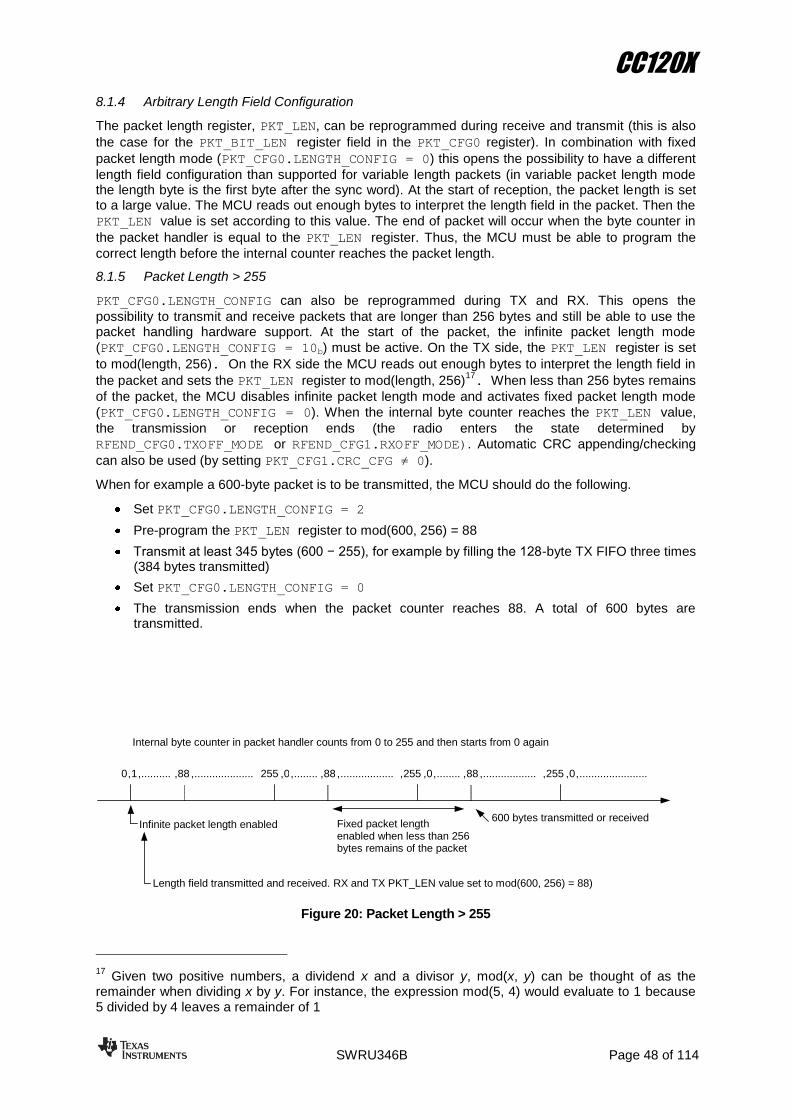
CC120X
SWRU346B Page 48 of 114
8.1.4 Arbitrary Length Field Configuration
The packet length register, PKT_LEN, can be reprogrammed during receive and transmit (this is also
the case for the PKT_BIT_LEN register field in the PKT_CFG0 register). In combination with fixed
packet length mode (PKT_CFG0.LENGTH_CONFIG = 0) this opens the possibility to have a different
length field configuration than supported for variable length packets (in variable packet length mode the length byte is the first byte after the sync word). At the start of reception, the packet length is set to a large value. The MCU reads out enough bytes to interpret the length field in the packet. Then the
PKT_LEN value is set according to this value. The end of packet will occur when the byte counter in
the packet handler is equal to the PKT_LEN register. Thus, the MCU must be able to program the
correct length before the internal counter reaches the packet length.
8.1.5 Packet Length > 255
PKT_CFG0.LENGTH_CONFIG can also be reprogrammed during TX and RX. This opens the
possibility to transmit and receive packets that are longer than 256 bytes and still be able to use the packet handling hardware support. At the start of the packet, the infinite packet length mode
(PKT_CFG0.LENGTH_CONFIG = 10b) must be active. On the TX side, the PKT_LEN register is set
to mod(length, 256). On the RX side the MCU reads out enough bytes to interpret the length field in
the packet and sets the PKT_LEN register to mod(length, 256)17. When less than 256 bytes remains
of the packet, the MCU disables infinite packet length mode and activates fixed packet length mode
(PKT_CFG0.LENGTH_CONFIG = 0). When the internal byte counter reaches the PKT_LEN value,
the transmission or reception ends (the radio enters the state determined by
RFEND_CFG0.TXOFF_MODE or RFEND_CFG1.RXOFF_MODE). Automatic CRC appending/checking
can also be used (by setting PKT_CFG1.CRC_CFG ≠ 0).
When for example a 600-byte packet is to be transmitted, the MCU should do the following.
Set PKT_CFG0.LENGTH_CONFIG = 2
Pre-program the PKT_LEN register to mod(600, 256) = 88
Transmit at least 345 bytes (600 − 255), for example by filling the 128-byte TX FIFO three times (384 bytes transmitted)
Set PKT_CFG0.LENGTH_CONFIG = 0
The transmission ends when the packet counter reaches 88. A total of 600 bytes are transmitted.
Figure 20: Packet Length > 255
17 Given two positive numbers, a dividend x and a divisor y, mod(x, y) can be thought of as the
remainder when dividing x by y. For instance, the expression mod(5, 4) would evaluate to 1 because 5 divided by 4 leaves a remainder of 1
0 , 1 , .......... , 88 , .................... 255 , 0 , ........ , 88 , .................. , 255 , 0 , ........ , 88 , .................. , 255 , 0 , .......................
Internal byte counter in packet handler counts from 0 to 255 and then starts from 0 again
Length field transmitted and received. RX and TX PKT_LEN value set to mod(600, 256) = 88)
Infinite packet length enabled Fixed packet length enabled when less than 256 bytes remains of the packet
600 bytes transmitted or received

CC120X
SWRU346B Page 49 of 114
8.1.6 Data Whitening
From a radio perspective, the ideal over the air data are random and DC free. This results in the smoothest power distribution over the occupied bandwidth. This also gives the regulation loops in the receiver uniform operation conditions (no data dependencies).
Real data often contain long sequences of zeros and ones making it difficult to track the data bits. In these cases, performance can be improved by whitening the data before transmitting, and de-whitening the data in the receiver.
With CC120X, this can be done automatically. By setting PKT_CFG1.WHITE_DATA = 1, all data,
except the preamble and the sync word will be XORed with a 9-bit pseudo-random (PN9) sequence before being transmitted. This is shown in Figure 21. At the receiver end, the data are XORed with the same pseudo-random sequence. In this way, the whitening is reversed, and the original data appear
in the receiver. The PN9 sequence is initialized to all 1’s. By setting PKT_CFG1.PN9_SWAP_EN = 1,
the PN9 sequence can be swapped before whitening/de-whitening. This can only be done when the
radio is using standard packet mode (PKT_CFG2.FG_MODE_EN = 0).
If CC120X is set up to transmit random data, the PN9 whitening sequence will be transmitted (see Table 25).
Figure 21: Data Whitening in TX Mode
Assume the following bytes should be transmitted: 0xAB, 0x80, 0xFF, 0x00
The first byte is XORed with 0xFF (initial value)
0xAB ⊕ 0xFF = 0x54
Table 25 shows how the bit shifting and XORing of bit 5 and bit 0 gives the bytes that the remaining bytes in the packet should be XORed with.
TX_OUT[7:0]
TX_DATA
8 7 6 5 4 3 2 1 0
7 6 5 4 3 2 1 0
The first TX_DATA byte is shifted in before doing the XOR-operation providing the first TX_OUT[7:0] byte. The
second TX_DATA byte is then shifted in before doing the XOR-operation providing the second TX_OUT[7:0] byte.

CC120X
SWRU346B Page 50 of 114
8 (5 ⊕ 0) 7 6 5 4 3 2 1 0
1 1 1 1 1 1 1 1 1
0 1 1 1 1 1 1 1 1
0 0 1 1 1 1 1 1 1
0 0 0 1 1 1 1 1 1
0 0 0 0 1 1 1 1 1
1 0 0 0 0 1 1 1 1
1 1 0 0 0 0 1 1 1
1 1 1 0 0 0 0 1 1
1 1 1 1 0 0 0 0 1
0 1 1 1 1 0 0 0 0
1 0 1 1 1 1 0 0 0
1 1 0 1 1 1 1 0 0
1 1 1 0 1 1 1 1 0
0 1 1 1 0 1 1 1 1
0 0 1 1 1 0 1 1 1
0 0 0 1 1 1 0 1 1
0 0 0 0 1 1 1 0 1
1 0 0 0 0 1 1 1 0
0 1 0 0 0 0 1 1 1
1 0 1 0 0 0 0 1 1
1 1 0 1 0 0 0 0 1
0 1 1 0 1 0 0 0 0
0 0 1 1 0 1 0 0 0
1 0 0 1 1 0 1 0 0
1 1 0 0 1 1 0 1 0
Table 25: PN9 Whitening Sequence
0x80 ⊕ 0xE1 = 0x61
0xFF ⊕ 0x1D = 0xE2
0x00 ⊕ 0x9A = 0x9A
.
.
.
The complete packet will look like this (assume default preamble, sync word, and CRC configuration):
0xAA, 0xAA, 0xAA, 0xAA, 0x93, 0x0B, 0x51, 0xDE, 0x54, 0x61, 0xE2, 0x9A, 0xF9, 0x9D
8.1.7 Data Byte Swap
If the PKT_CFG2.BYTE_SWAP_EN register field is set than the bits in each byte are swapped,
meaning that bit 0 becomes bit 7, bit 1 becomes bit 6 etc. until bit 7 becomes bit 0.
In TX mode all bytes in the TX FIFO are swapped before optional CRC calculation and whitening are performed.
In RX mode the data byte is swapped after all the processing is done, meaning that de-whitening and CRC calculation are done on the original received data, and the swapping is done right before the actual writing to the RX FIFO. This means that if using address filtering (see Section 8.2.1) is used
when PKT_CFG2.BYTE_SWAP_EN, the user should swap the address manually in the DEV_ADDR
register in order to match the received address due to the fact that the packet engine compares the address register to the received address before the swapping is done.
Figure 22 shows the data sent over the air vs. the data written to the TX FIFO when byte swap is enabled (assume that whitening and CRC calculation are disabled). If the receiver uses address filtering, the address should be programmed to be 0xEA.

CC120X
SWRU346B Page 51 of 114
0 0 0 0 0 0 1 1 0 1 0 1 0 1 1 1 0 0 1 0 0 1 1 0 1 0 1 1 0 0 1 0
0x03 0x57 0x26 0xB2
1 1 0 0 0 0 0 0 1 1 1 0 1 0 1 0 0 1 1 0 0 1 0 0 0 1 0 0 1 1 0 1
0xC0 0xEA 0x64 0x4D
Data written to TX FIFO
Data sent on the air
Figure 22: Data Byte Swap
8.1.8 UART Mode
If UART mode is enabled (PKT_CFG0.UART_MODE_EN = 1), the packet engine inserts and removes
start/stop bits automatically. In this mode the packet engine will emulate UART back-to-back transmissions typically done over an asynchronous RF interface, to enable communication with simple RF devices without packet support.
The start and stop bits are not handled as data, only inserted/removed in the data stream to/from the modem, hence all packet features are available in this mode. The value of the start/stop bits is
configurable through the PKT_CFG0.UART_SWAP_EN register field.
If whitening is enabled, only the data bits are affected, not the start/stop bits.
A "framing error" occurs in RX mode when the designated "start" and "stop" bits are not received as expected. As the "start" bit is used to identify the beginning of an incoming byte it acts as a reference for the remaining bits. If the "start" and "stop" bits are not in their expected value, it means that the
data is not in line and a framing error will occur (the UART_FRAMING_ERROR signal will be asserted).
Framing errors will not stop the on-going reception.

CC120X
SWRU346B Page 52 of 114
8.2 Packet Filtering in Receive Mode
CC120X supports three different types of packet-filtering; address filtering, maximum length filtering, and CRC filtering.
8.2.1 Address Filtering
Setting PKT_CFG1.ADDR_CHECK_CFG to any other value than zero enables the address filtering
where the packet handler engine will compare the address field in the packet (see Figure 19) with the
programmed node address in the DEV_ADDR register. If PKT_CFG1.ADDR_CHECK_CFG = 10b it will
in addition check against the 0x00 broadcast address, or both the 0x00 and 0xFF broadcast
addresses when PKT_CFG1.ADDR_CHECK_CFG = 11b. If the received address matches a valid
address, the packet is received and written into the RX FIFO. If the address match fails, the packet is discarded and the radio controller will either restart RX or go to IDLE dependent on the
RFEND_CFG0.TERM_ON_BAD_PACKET_EN setting (the RFEND_CFG1.RXOFF_MODE setting is
ignored18
).
8.2.2 Maximum Length Filtering
In variable packet length mode, PKT_CFG0.LENGTH_CONFIG = 01, the PKT_LEN register value is
used to set the maximum allowed packet length. If the received length byte has a larger value than this, the packet is discarded and the radio controller will either restart RX or go to IDLE dependent on
the RFEND_CFG0.TERM_ON_BAD_PACKET_EN setting (the RFEND_CFG1.RXOFF_MODE setting is
ignored).
8.2.3 CRC Filtering
The filtering of a packet when CRC check fails is enabled by setting
FIFO_CFG.CRC_AUTOFLUSH = 1. The CRC auto flush function will only flush the packet received
with bad CRC, other packets will remain unchanged in the RX FIFO. After auto flushing the faulty packet, the radio controller will either restart RX or go to IDLE dependent on the
RFEND_CFG0.TERM_ON_BAD_PACKET_EN setting (the RFEND_CFG1.RXOFF_MODE setting is
ignored).
When using the auto flush function, the maximum packet length is 127 bytes in variable packet length
mode and 128 bytes in fixed packet length mode. Note that when PKT_CFG1.APPEND_STATUS is
enabled, the maximum allowed packet length is reduced by two bytes in order to make room in the RX FIFO for the two status bytes appended at the end of the packet. The MCU must not read from the current packet until the CRC has been checked as OK.
0123456789
1011121314151617
.
.
.
124125126127
0123456789
1011121314151617
.
.
.
124125126127
0123456789
1011121314151617
.
.
.
124125126127
0123456789
1011121314151617
.
.
.
124125126127
0123456789
1011121314151617
.
.
.
124125126127
RXLAST
RXLAST
RXLAST RXLAST
RXLAST
CRC Error
1st packet CRC OK
2nd packet CRC OK
3rd packet CRC Error
4th packet CRC OK
RXLAST
RX FIFO is empty
Figure 23: CRC Autoflush of Faulty Packet
18 RFEND_CFG1.RXOFF_MODE can be changed while in active mode

CC120X
SWRU346B Page 53 of 114
8.2.4 Auto Acknowledge
By configuring the radio to enter TX after a packet has been received (RFEND_CFG1.RXOFF_MODE =
TX) and enabling termination on bad packets (RFEND_CFG0.TERM_ON_BAD_PACKET_EN = 1)
automatic acknowledgement of packets can be achieved. The Ack. packet should be written to the TX FIFO before RX mode is being entered. With the settings described above, receiving a bad packet (error in address, length, or CRC) will have the radio enter IDLE state while receiving a good packet will cause the radio to enter TX state and transmit the packet residing in the TX FIFO.
8.3 Packet Handling in Transmit Mode
The payload that is to be transmitted must be written into the TX FIFO. The first byte written must be
the length byte when variable packet length is enabled (PKT_CFG0.LENGTH_CONFIG = 1). The
length byte has a value equal to the payload of the packet (including the optional address byte). If
address recognition is enabled in the receiver (PKT_CFG1.ADDR_CHECK_CFG ≠ 0) the second byte
written to the TX FIFO must be the address byte (as the address in not automatically inserted).
If fixed packet length is enabled (PKT_CFG0.LENGTH_CONFIG = 0), the first byte written to the TX
FIFO should be the address (assuming the receiver uses address recognition).
The modulator will first send the programmed number of preamble bytes configured through the
PREAMBLE_CFG1.NUM_PREAMBLE register field. If data is available in the
TX FIFO, the modulator will send the sync word (programmed through SYNC_CFG1.SYNC_MODE and
SYNC3/2/1/0) followed by the payload in the TX FIFO. If CRC is enabled
(PKT_CFG1.CRC_CFG ≠ 0), the checksum is calculated over all the data pulled from the TX FIFO,
and the result is sent as two extra bytes following the payload data. If the TX FIFO runs empty before the complete packet has been transmitted, the radio will enter TX_FIFO_ERR state. The only way to
exit this state is by issuing an SFTX strobe. Writing to the TX FIFO after it has underflowed will not
restart TX mode.
If whitening is enabled, everything following the sync words will be whitened. Whitening is enabled by
setting PKT_CFG1.WHITE_DATA = 1. For more details on whitening, please see Section 8.1.6.
8.4 Packet Handling in Receive Mode
In receive mode, the radio will search for a valid sync word (if SYNC_CFG1.SYNC_MODE ≠ 0) and
when found, the demodulator has obtained both bit and byte synchronization and will receive the first payload byte. For more details on byte synchronization/sync word detection, please see Section 6.7
If whitening is enabled (PKT_CFG1.WHITE_DATA = 1), the data will be de-whitened at this stage.
When variable packet length mode is enabled (PKT_CFG0.LENGTH_CONFIG = 1), the first byte is
the length byte. The packet handler stores this value as the packet length and receives the number of bytes indicated by the length byte. If fixed packet length mode is used
(PKT_CFG0.LENGTH_CONFIG = 0), the packet handler will accept the number of bytes programmed
through the PKT_LEN.PACKET_LENGHT register field.
Next, the packet handler optionally checks the address (if PKT_CFG1.ADDR_CHECK_CFG ≠ 0) and
only continues the reception if the address matches. If automatic CRC check is enabled
(PKT_CFG1.CRC_CFG ≠ 0), the packet handler computes CRC and matches it with the appended
CRC checksum.
At the end of the payload, the packet handler will optionally write two extra packet status bytes (see Table 23 and Table 24) that contain CRC status, LQI, and RSSI value if
PKT_CFG1.APPEND_STATUS = 1.
8.5 Packet Handling in Firmware
When implementing a packet oriented radio protocol in firmware, the MCU needs to know when a packet has been received/transmitted. Additionally, for packets longer than 128 bytes, the RX FIFO needs to be read while in RX and the TX FIFO needs to be refilled while in TX. This means that the MCU needs to know the number of bytes that can be read from or written to the RX FIFO and TX FIFO respectively. There are two possible solutions to get the necessary status information:

CC120X
SWRU346B Page 54 of 114
a) Interrupt Driven Solution
The GPIO pins can be used in both RX and TX to give an interrupt when a sync word has been received/transmitted or when a complete packet has been received/transmitted by setting
IOCFGx.GPIOx_CFG = PKT_SYNC_RXTX (6). In addition, there are four configurations for the
IOCFGx.GPIOx_CFG register that can be used as an interrupt source to provide information on how
many bytes are in the RX FIFO and TX FIFO respectively (see 8.6 for more details).
b) SPI Polling
The GPIO_STATUS register can be polled at a given rate to get information about the current GPIO
values. The NUM_RXBYTES and NUM_TXBYTES registers can be polled at a given rate to get
information about the number of bytes in the RX FIFO and TX FIFO respectively. It is also possible to
use FIFO_NUM_RXBYTES.FIFO_RXBYTES and FIFO_NUM_TXBYTES.FIFO_TXBYTES. These
register fields give the number of bytes available in the RX FIFO and free bytes in the TX FIFO, and both register values saturates at 15.
8.6 TX FIFO and RX FIFO
The CC120X contains two 128 byte FIFOs, one for received data and one for transmit data. The SPI interface is used to read from the RX FIFO and write to the TX FIFO. Section 3.2.4 contains details on the SPI FIFO access. The FIFO controller will detect under/overflow in both the RX FIFO and the TX FIFO.
A signal will assert when the number of bytes in the FIFO is equal to or higher than a programmable threshold. This signal can be viewed on the GPIO pins and can be used for interrupt driven FIFO
routines to avoid polling the NUM_RXBYTES and NUM_TXBYTES registers. The IOCFGx.GPIOx_CFG
= RXFIFO_THR (0) and the IOCFGx.GPIOx_CFG = RXFIFO_THR_PKT (1) configurations are
associated with the RX FIFO while the IOCFGx.GPIOx_CFG = TXFIFO_THR (2) and the
IOCFGx.GPIOx_CFG = TXFIFO_THR_PKT (3) configurations are associated with the TX FIFO.
The 7-bit FIFO_CFG.FIFO_THR setting is used to program threshold points. Table 26 lists the
FIFO_THR settings and the corresponding thresholds for the RX and TX FIFO. The threshold value is
coded in opposite directions for the two FIFOs to give equal margin to the overflow and underflow conditions when the threshold is reached.
FIFO_THR Bytes in TX FIFO Bytes in RX FIFO
0 127 1
1 126 2
2 125 3
... ... ...
126 1 127
127 0 128
Table 26: FIFO_THR Settings and the Corresponding FIFO Thresholds
To simplify debug and advanced FIFO features, the full FIFO buffer is memory mapped and can be accessed directly(see Section 3.2.3). Both FIFO content and FIFO data pointers are accessible. This can be used to significantly reduce the SPI traffic, see examples below
1. In a hostile RF environment packets are lost and re-transmissions are often required. Normally the packet data must then be written again over the SPI interface. By using the direct FIFO
access feature and changing the TXFIRST register to point to the head of the previous
message, a re-transmission can be done without writing the packet over the SPI.
2. In many protocols only parts of the message is changed between each transmission (e.g. changing a read value from a sensor, incrementing a transmission counter). Direct FIFO access can then be used to change only the new data (the FIFOs are reached through the 0x3E command, see Table 4), leaving the rest of the data unchanged. FIFO data pointers
(TXFIRST and TXLAST) can then be manipulated to re-transmit the packet with changed data.

CC120X
SWRU346B Page 55 of 114
8.7 IEEE 802.15.4g Support
802.15.4g hardware support is enabled by setting PKT_CFG2.FG_MODE_EN = 1. This will override
all other packet configurations. The only register fields that will be recognized are
PKT_CFG1.CRC_CFG, PKT_CFG1.APPEND_STATUS and PKT_CFG2.BYTE_SWAP_EN. To be
compliant to the 802.15.4g standard PKT_CFG2.BYTE_SWAP_EN must be set to 0.
8.7.1 802.15.4g Packet Format
The format of the 802.15.4g packet format supported by the radio can be seen in Figure 24.
Preamble bits
(Programmable)
Sta
rt F
ram
e
De
limite
r
PH
RA
fie
ld
PH
RB
fie
ld
Data field
CR
C-3
2
or
CR
C1
6
CRC calculation
8 x 4 bits 2 x 16 bits8
bits
8
bits8 x n bits
32 or 16
bits
Optional data whitening
Legend:
Inserted automatically in TX,
processed and removed in RX.
Unprocessed user data (Except for
whitening)
Figure 24: 802.15.4g Packet Format
PHRA and PHRB in Figure 24 corresponds to PHR[15:8] and PHR[7:0] in the 802.15.4g standard [3] (see Figure 25 and Figure 26). The radio supports normal 802.15.4g packets (i.e. packets without MS (Mode Switch)). MS packets must be handled by software.
PHRA[7] PHRA[6:5] PHRA[4] PHRA[3] PHRA[2:0]: PHRB[7:0]
PHR[15] PHR[14:13] PHR[12] PHR[11] PHR[10:0]
Bit String Index 0 1 - 2 3 4 5 - 15
Bit Mapping MS R1 - R0 FCS DW L10 - L0
Field Name Mode switch Reserved FCS type Data whitening Frame length
Figure 25: Format of PHR without Mode Switch
PHRA[7] PHRA[6:5] PHRA[4] PHRA[3:0]: PHRB[7:5] PHRB[4:1] PHRB[0]
PHR[15] PHR[14:13] PHR[12] PHR[11:5] PHR[4:1] PHR[0]
Bit String Index 0 1 - 2 3 4 - 10 11 - 14 15
Bit Mapping MS M1 - M0 FEC - B3 - B0 PC
Field Name Mode switch
Mode switch parameter entry
New mode FEC
New mode Checksum Parity check
Figure 26: Format of PHR with Mode Switch

CC120X
SWRU346B Page 56 of 114
8.7.2 802.15.4g Packet Control
The radio will support TX and RX with normal 802.15.4g packets (i.e. non Mode Switch packets). All handling of Mode Switch packets must be entirely done in SW.
8.7.2.1 802.15.4g TX Packets
When transmitting an 802.15.4g packet the format must comply with the format shown in Figure 24. It is up to the application to write a correct PHR bytes and payload to the TXFIFO. The radio will check for Mode Switch (MS) and that the frame length is within the specifications before transmitting the packet. If MS is not set and the frame length complies with the standard the radio will check the Data Whitening (DW) bit field and the Frame Check Sequence (FCS) bit field and apply whitening and FCS according to the bit fields. The transmission flow is outlined in Figure 27.
ModeSwitch(MS)?
Send packet without
CRC16/CRC32
Yes
Send packet with CRC16/CRC32
Framelength valid ?
Yes
No
Abort transmissionNo error code
Assert done
802.15.4g mode and STX
No
Figure 27: Transmission Flow in 802.15.4g Mode

CC120X
SWRU346B Page 57 of 114
8.7.2.2 802.15.4g RX Packets
The radio supports reception of normal (non Mode Switch) 802.15.4g packets. If the MS bit is not set and the frame length is valid, the radio will receive the rest of the payload according to the PHR configuration. If a Mode Switch packet is received or the frame length field is not valid, the radio will abort RX and the Mode Switch frame (PHR bytes) will be available in the RXFIFO. RSSI for Mode Switch packets is not available. Figure 28 outlines the reception flow for an 802.15.4g packet.
Successful 15.4g packet
802.15.4g mode and SRX
ModeSwitch(MS)or
Illegal framelength?
Receive PHR
Abort reception assert pkt_length_failed
Yes
Continue PHR-configured reception
No
MS part of system?
Assert done with appropiate status
15.4g packet has failed
Marc_status=0x80
SW: Run BCH(15,11) and parity check on
PHR to check for MS-packet
Yes No
Yes
No
HW
SW(abstraction routine)Successful reception
(MS should be performed in parallell)
MS packet
Return to MAC layer
NoSuccessful 15.4g MS
packetYes
Figure 28: 802.15.4g Packet Reception

CC120X
SWRU346B Page 58 of 114
8.7.3 802.15.4g Append Status
If the PKT_CFG1.APPEND_STATUS bit is set, two status bytes containing information on CRC, LQI
and RSSI will be written to the RXFIFO.
Bit Field Name Description
7:0 RSSI RSSI value
Table 27. Received Packet Status Byte 1 (first byte appended after the data)
Bit Field Name Description
7 CRC_OK 1: CRC32 OK if FCS type = 0 and CRC32 is OK 1: CRC16 OK if FCS type = 1 and CRC16 is OK 0: CRC error in received data
6:0 LQI Indicating the link quality
Table 28: Received Packet Status Byte 2 (second byte appended after the data)
8.7.4 802.15.4g Data Byte - Bit Swapping
If the PKT_CFG1.BYTE_SWAP_EN register field is set than the bits in each byte are swapped,
meaning that bit 0 become 7, bit 1 become bit 6 etc. until bit 7 becomes bit 0.
In TX mode all bytes in the TX FIFO are swapped before optional CRC calculation and whitening are performed.
In RX mode the data byte is swapped after all the processing is done, meaning that de-whitening and CRC calculation are done on the original received data, and the swapping is done right before the actual writing to the RX FIFO.
Bit swapping should be turned off to be compliant with the 802.15.4g standard.
8.7.5 802.15.4g Data Whitening
Data whitening of the payload is defined by the Data Whitening field (DW) in the PHR. If this bit is set all data except the preamble, SFD and PHR field will be XOR-ed with a 9-bit pseudo-random (PN9) sequence before being transmitted. At the receiver the DV bit of the PHR is read and the data is XOR-ed with the same pseudo-random sequence to de-white the data back to its original form.
The PN9 generator is defined as seen in Figure 29. The seed in the PN9 generator is set to all 1’s and is reinitialized after each packet.
D D D D D D D D D
PN9
Figure 29: PN9 Generator

CC120X
SWRU346B Page 59 of 114
8.8 802.15.4g Frame Check Sequence (FCS)
The radio supports both a 16-bit CRC and a 32-bit CRC for the Frame Check Sequence (FCS). The type to be used is defined by the FCS field in the PHR bytes. The length of the FCS must be added to Frame Length of the PHR in order to have a valid 802.15.4g packet. It is the applications responsibility that PHR fields are correct. Table 29 shows the relationship between the FCS Type field and the transmitted CRC bytes.
FCS Type Field Value Transmitted FCS Length
0 4 byte
1 2 byte
Table 29: Transmitted FCS Length
8.8.1 802.15.4g Forward Error Correction (FEC)
A Non Recursive and Non Systematic Code (NRNSC) encoder is implemented to support FEC for 802.15.4g. FEC is optional for 802.15.4g and is indicated by the synchronization word used for the packet.
In addition to set PKT_CFG2.FG_MODE_EN = 1, the following register fields must be set to enable
802.15.4g FEC support:
PKT_CFG1.FEC_EN = 1
SYNC_CFG1.SYNC_MODE = 7 (DualSync Search)
When receiving an 802.15.4g packet the receiver will check the sync word received and if it matches
the sync word contained in the two high bytes fields in the sync word registers (SYNC3 and SYNC2) it
will assume that the packet is FEC encoded.
When transmitting a FEC encoded 802.15.4g packet it is important to have the FEC defined sync
word written to the SYNC1 and SYNC0 register field as the CC120X will always send the sync word
contained in the lower end of the sync word registers when SYNC_CFG1.SYNC_MODE = 7.
8.9 Transparent and Synchronous Serial Operation
Several features and modes of operation have been included in the CC120X to provide backward compatibility with legacy systems that cannot be supported by the built in packet handling functionality. For new systems, it is recommended to use the built-in packet handling features, as they give more robust communication, significantly offload the microcontroller, and simplify software development. There are two serial modes and they are described in the two following sections.
Serial mode is only supported for 2’ary modulations. The exception in synchronous serial mode (RX)
which also supports 4’ary modulation formats. Figure 30 shows SERIAL_CLK and SERIAL_RX for the
data 0xAA for both 2-FSK and 4-FSK. The symbol rate is the same in both cases.
1 0 1 0 1 0 1 0
01010101
t
2t
Time
2-FSK
4-FSK
SERIAL_RX
SERIAL_CLK
SERIAL_RX
SERIAL_CLK
Figure 30: 2’ary vs. 4’ary Modulation Format in Serial Mode

CC120X
SWRU346B Page 60 of 114
8.9.1 Synchronous Serial Mode
In the synchronous serial mode, data is transferred on a two-wire serial interface. The CC120X
provides a clock (IOCFGx.GPIOx_CFG = SERIAL_CLK (8)) that is used to set up new data on the
data input line or sample data on the data output line. Data timing recovery is done automatically. The data pin is updated on the falling edge of the clock pin at the programmed symbol rate. Sync word insertion/detection may or may not be active, depending on the sync mode. If sync word detection is
enabled (SYNC_CFG1.SYNC_MODE ≠ 0) the serial clock (SERIAL_CLK) will not be output on the
GPIO before a sync word is transmitted/received. When SYNC_MODE = 0 (blind mode) it is
recommended to transmit a minimum of 4 bytes preamble.
Define a GPIO pin to be serial data clock for both TX and RX operation. For RX operation, another
GPIO pin has to be defined as serial data output (IOCFGx.GPIOx_CFG = SERIAL_RX (9)).
For TX operation, the GPIO0 pin is explicitly used as serial data input. This is automatically done when in TX. In order to avoid internal I/O conflict, GPIO0 should be defined as tri-state. GPIO0 will be automatically tri-stated in TX if the GPIO0 is defined as serial clock or serial data output
(IOCFG0.GPIO0_CFG = 8 or 9). If this is not the case, GPIO0 must be manually tri-stated by
setting IOCFG0.GPIO0_CFG = HIGHZ (48).
In synchronous serial mode the TX data must be set up on the falling edge of the data clock output
from CC120X.
In addition to set PKT_CFG2.PKT_FORMAT = 1, the following register fields must be set:
MDMCFG1.FIFO_EN = 0
MDMCFG0.TRANSPARENT_MODE_EN = 0
IOCFGx.GPIOx_CFG = 001001b (SERIAL_RX. Only necessary for RX mode)
IOCFGx.GPIOx_CFG = 001000b (SERIAL_CLK)
SERIAL_STATUS.IOC_SYNC_PINS_EN = 1 (Only necessary for TX mode19
)
PREAMBLE_CFG1.NUM_PREAMBLE = 0
Synchronous serial mode is often used in applications needing to be backward compatible, and sync
detection is disabled (SYNC_CFG1.SYNC_MODE = 0) since the format of the sync word often do not
match the supported sync word format. Best radio performance is however achieved when
SYNC_MODE ≠ 0. In cases where the packet has a preamble but not a sync word that matches the
sync format supported by the CC120X, the radio can simply use the preamble as a sync word. Consider the case where a receiver wants to receive packets with 3 different addresses but no common sync word:
Packet 1: 0xAA, 0xAA, 0xAA, 0xAA, Address1, Data0, Data 1, Data 2, …
Packet 1: 0xAA, 0xAA, 0xAA, 0xAA, Address2, Data0, Data 1, Data 2, …
Packet 1: 0xAA, 0xAA, 0xAA, 0xAA, Address3, Data0, Data 1, Data 2, …
By setting SYNC_CFG1.SYNC_MODE = 010b and SYNC1 = SYNC0 = 0xAA a sync word is detected
somewhere within the preamble and the serial clock will be output on a GPIO when SYNC_EVENT is
asserted. Now the MCU can manually start searching for the 3 different addresses. When this method
is used TOC_CFG.TOC_LIMIT should be 0. In blind mode, TOC_LIMIT must be 1 or 11b.
19 If this bit is set in RX mode, GPIO2 must be hardwired to 0 (IOCFG2.GPIO2_CFG = HW0 (51))

CC120X
SWRU346B Page 61 of 114
8.9.2 Transparent Serial Mode
CC120X does not do any timing recovery and just outputs the hard limited baseband signal. In transparent serial mode the symbol rate programming does not affect operation. When transparent mode is enabled, the device is set up to resemble a legacy purely analog front end device with baseband output to support legacy pulse position modulation, PWM modulated signals etc. In transparent mode the signal is digitally demodulated and output on GPIO pins through a
programmable interpolation filter (MDMCFG0.TRANSPARENT_INTFACT). The interpolation filter is used
to eliminate jitter on the baseband signal. This is useful when using external DSP demodulators as jitter introduce noise in the demodulation process. The rate on the GPIO is ((4 x receiver bandwidth) x interpolation factor).
When using transparent serial mode make sure the interfacing MCU/DSP does proper oversampling. In transparent serial mode, several of the support mechanisms for the MCU that are included in
CC120X will be disabled, such as packet handling hardware, buffering in the FIFO, and so on.
Preamble and sync word insertion/detection is not supported in transparent serial mode.
For TX operation, the GPIO0 pin is explicitly used as serial data input. This is automatically done when in TX. In order to avoid internal I/O conflict, GPIO0 should be defined as tri-state. GPIO0 will be automatically tri-stated in TX if the GPIO0 is defined as serial clock or serial data output
(IOCFG0.GPIO0_CFG = 8 or 9). If this is not the case, GPIO0 must be manually tri-stated by
setting IOCFG0.GPIO0_CFG = HIGHZ (48).
Data output can be observed on GPIO0/1/2/3. This is set by the IOCFGx.GPIOx_CFG fields.
In addition to set PKT_CFG2.PKT_FORMAT = 11b, the following register fields must be set:
MDMCFG1.FIFO_EN = 0
MDMCFG0.TRANSPARENT_MODE_EN = 1
IOCFGx.GPIOx_CFG = 001001b (SERIAL_RX. Only necessary for RX mode)
SERIAL_STATUS.IOC_SYNC_PINS_EN = 1 (Only necessary for TX mode)
In transparent mode, the frequency offset correction is calculated based on the incoming samples clocked with a rate equal to 2·RX filter BW. If the data stream contains a row of equal symbols the correction factor will move too far to one side with reduced sensitivity as a result. For systems where it is not possible to have a white data stream the following may be done to improve sensitivity:
Set FREQOFF_CFG.FOC_KI_FACTOR = 3 to select the slowest loop
For a system where the frequency error is less than the deviation the frequency offset
correction may be turned off by setting FREQOFF_CFG.FOC_EN = 0

CC120X
SWRU346B Page 62 of 114
9 Radio Control
CC120X has a built-in state machine that is used to switch between different operational states (modes). The change of state is done either by using command strobes or by internal events such as TX FIFO underflow. A simplified state diagram is shown in Figure 2. The numbers refer to the state
numbers readable from the MARCSTATE.MARC_STATE register field.
9.1 Power-On Start-Up Sequence
When the power supply is turned on, the system must be reset. This is achieved by one of the two sequences described below, i.e. automatic power-on reset (POR) or manual reset.
9.1.1 Automatic POR
A power-on reset circuit is included in the CC120X. The internal power-up sequence is completed when
CHIP_RDYn goes low. CHIP_RDYn is observed on the SO pin after CSn is pulled low (See Section
3.1.2 for more details).
When the CC120X reset is completed, the chip will be in the IDLE state and the crystal oscillator will be running. If the chip has had sufficient time for the crystal oscillator to stabilize after the power-on-reset, the SO pin will go low immediately after taking CSn low. If CSn is taken low before reset is completed, the SO pin will first go high, indicating that the crystal oscillator is not stabilized, before going low as shown in Figure 31.
XOSC Stable
CSn
SO
Figure 31: Power-On Reset
9.1.2 Manual Reset
The other reset possibilities on the CC120X are issuing using the SRES command strobe or using the
RESET_N pin. By issuing a manual reset, all internal registers are set to their default values and the radio will enter IDLE state.
9.2 Crystal Control
The crystal oscillator (XOSC) is either automatically controlled or always on, if
XOSC2.XOSC_CORE_PD_OVERRIDE = 1. If the XOSC is forced on, the crystal will always stay on
even if an SXOFF, SPWD, or SWOR command strobe has been issued. This can be used to enable fast
start-up from SLEEP/XOFF at the expense of a higher current consumption. If
XOSC2.XOSC_CORE_PD_OVERRIDE = 0, the XOSC will be turned off if the SXOFF, SPWD, or SWOR
command strobes are issued; the state machine then goes to XOFF or SLEEP state. This can only be done from the IDLE state. The XOSC will be automatically turned on again when CSn goes low, and the radio will enter IDLE state. The SO pin on the SPI interface must be pulled low before the SPI interface is ready to be used, as described in Section 3.1.2.
Crystal oscillator start-up time depends on crystal ESR and load capacitances.
9.3 Voltage Regulator Control
The voltage regulator to the digital core is controlled by the radio controller. When the chip enters the SLEEP state which is the state with the lowest current consumption, the voltage regulator is disabled.
This occurs after CSn is released when a SPWD or SWOR command strobe has been sent on the SPI
interface. The chip is then in the SLEEP state. Setting CSn low again will turn on the regulator and crystal oscillator and make the chip enter the IDLE state.

CC120X
SWRU346B Page 63 of 114
9.4 Active Modes
CC120X has two active modes: receive (RX) and transmit (TX). These modes are activated directly by
the MCU by using the SRX and STX command strobes, or automatically by eWOR (RX mode).
The MCU can manually change the state from RX to TX and vice versa by using the command
strobes. If the radio controller is currently in transmit and the SRX strobe is used, the current
transmission will be ended and the transition to RX will be done. If the radio controller is in RX when
the STX or SFSTXON command strobes are used, the TX-on-CCA function will be used. If the channel
is clear, TX (or FSTXON state) is entered. The PKT_CFG2.CCA_MODE setting controls the conditions
for clear channel assessment (see Section 6.11 for more details).
The SIDLE command strobe can always be used to force the radio controller to go to the IDLE state.
9.4.1 RX
When RX is activated, the chip will remain in receive mode until:
A packet is received
An SIDLE, SRX20
, STX, or SFSTXON command strobe is being issued
The RX FIFO overflows/underflows
The RX termination timer expires
A CS or PQT based termination takes place
When a packet is successfully received, the radio controller goes to the state indicated by the
RFEND_CFG1.RXOFF_MODE setting, i.e. IDLE, FSTXON, TX or RX. When a bad packet is received
(packet length/address/CRC error) the radio controller will either restart RX or go to IDLE depending
on the RFEND_CFG0.TERM_ON_BAD_PACKET_EN setting.
When an RX FIFO overflow or underflow occurs, the radio will enter RX_FIFO_ERR state. When RX terminates due to the RX termination timer or lack of CS/PQT, the radio will enter IDLE mode (via
CALIBRATE depending on the SETTLING_CFG.FS_AUTOCAL setting).
Please see Section 9.6 for details on which states the radio enters after RX when eWOR is used.
9.4.2 TX
Similarly, when TX is active the chip will remain in the TX state until:
The current packet has been transmitted
An SIDLE or SRX command strobe is being issued
The TX FIFO overflows/underflows
When a packet is successfully transmitted, the radio controller goes to the state indicated by the
RFEND_CFG0.TXOFF_MODE setting. The possible destinations are the same as for RX.
20 When an SRX strobe is issued in RX state, RX is restarted (the modulator starts searching for a
sync word). If the radio was in the middle of a packet reception, part of the “old” packet will remain in
the RX FIFO so NUM_RXBYTES or RX_LAST should be read before strobing SRX to keep track of
where the old and new packets are located in the RX FIFO.

CC120X
SWRU346B Page 64 of 114
9.5 RX Termination
RX can be terminated by the use of an RX termination timer or based on the assertion of
CARRIER_SENSE and/or PQT_REACHED. When RX terminates, the chip will always go back to IDLE if
eWOR is disabled and back to SLEEP (via IDLE) if eWOR is enabled.
9.5.1 RX Termination Timer
CC120X has functionality to allow for automatic termination of RX after a programmable timeout. The main use for this functionality is in eWOR mode, but it is also useful for other applications as it reduces the need for a dedicated MCU timer. The termination timer starts when the chip has entered
RX state, and the timeout is programmable with the RFEND_CFG1.RX_TIME setting. When the timer
expires, the radio controller will check the condition for staying in RX.
The programmable conditions are:
RFEND_CFG1.RX_TIME_QUAL = 0: Continue receive if sync word has been found
RFEND_CFG1.RX_TIME_QUAL = 1: Continue receive if sync word has been found, or if PQT
is reached or CS is asserted
Equation 22 can be used to calculate the RX timeout.
[s] 1250
22
0,1Timeout RX _4
3_
XOSC
RESWOR
TIMERX f
EVENTFLOORMAX
Equation 22: RX Timeout
EVENT0 is programmed through WOR_EVENT0_MSB and WOR_EVENT0_LSB, RX_TIME is found in
RFEND_CFG1 and WOR_RES in WOR_CFG1.
Figure 32 shows how the radio stays in RX until a packet has been received since a sync word was found before the RX termination timer expired (after 10 ms).
RX
Time [ms]
1 2 3 4 5
Preamble Sync Payload CRC
IDLE IDLE
14 15 16
RX_TIME_QUAL = 0
No sync found after 10 ms
RX
1 2 3 4 5
IDLE IDLE
14 15 16
RX_TIME_QUAL = 0
Sync found within 10 ms
17 18 19 20Time [ms]
Figure 32: RX Termination when RX_TIME_QUAL = 0 (RX Timeout = 10 ms)

CC120X
SWRU346B Page 65 of 114
Figure 33 shows how the radio behaves when RX_TIME_QUAL = 1 (assume that
RFEND_CFG0.ANT_DIV_RX_TERM_CFG = 0). When the RX termination timer expires, the radio will
check if a sync word is found or if CARRIER_SENSE or PQT_REACHED has been asserted (to check on
PQT_REACHED, PREAMBLE_CFG0.PQT_EN should be set). If this is the case the radio will remain in
RX until a packet has been received. This is the case even if the condition for staying in RX is no longer true. As shown in the figure, the radio remains in RX after the 10 ms timeout even if a
preamble is no longer present (PQT_REACHED will be de-asserted) as it only checks the condition for
staying in RX once when the termination timer expires. The radio will not exit RX mode until a packet has been received.
RX
Time [ms]
1 2 3 4 5
Preamble Sync Payload CRC
IDLE IDLE
14 15 16
RX_TIME_QUAL = 1
No sync found after 10 ms
RX
1 2 3 4 5
IDLE IDLE
21 22
RX_TIME_QUAL = 1
Preamble found within 10 ms
23 24 2520Time [ms]
Preamble
RX
1 2 3 4 5
IDLE IDLE
31 32
RX_TIME_QUAL = 1Preamble found within 10 ms
33Time [ms]
Preamble Sync Payload CRC
Figure 33: RX Termination when RX_TIME_QUAL = 1 (RX Timeout = 10 ms)

CC120X
SWRU346B Page 66 of 114
9.5.2 RX Termination Based on CS
If RFEND_CFG0.ANT_DIV_RX_TERM_CFG = 1 the device will use the first RSSI sample to
determine if a carrier is present in the channel. If no carrier is present (CARRIER_SENSE not
asserted), RX will terminate. The RSSI samples are continually evaluated, and if the RSSI level falls
below the threshold (programmed through the AGC_CS_THR register) RX will terminate if not sync is
found. This can be used to achieve very low power by reducing the time in RX mode to a minimum.
Figure 34 shows how RX mode will be terminated based on CS for different scenarios. Note that sync detection will keep the radio in RX until the packet is received regardless of the state of the
CARRIER_SENSE signal.
RX
1 2 3 4 5
IDLE
14
RX_TIME_QUAL = 0
RFEND_CFG0.ANT_DIV_RX_TERM_CFG = 001b
AGC_CARRIER_SENSE
IDLE
15 16
RX
1 2 3 4 5
IDLE
14
RX_TIME_QUAL = 0
RFEND_CFG0.ANT_DIV_RX_TERM_CFG = 001b
AGC_CARRIER_SENSE
IDLE
15 16
Time [ms]
Time [ms]
RX
1 2 3 4 5
IDLE
14
RX_TIME_QUAL = 0
RFEND_CFG0.ANT_DIV_RX_TERM_CFG = 001b
CARRIER_SENSE
IDLE
15 16
Time [ms]
RX
1 2 3 4 5
IDLE
14
RX_TIME_QUAL = 1
RFEND_CFG0.ANT_DIV_RX_TERM_CFG = 001b
CARRIER_SENSE
IDLE
15 16
Time [ms]
RX terminated due to lack of carrier
RX terminated when carrier is no longer present
RX terminated at RX timeout due to no sync word found (RX_TIME_QUAL = 0)
RX terminated when carrier is no longer present (not terminated at RX timeout since carrier is present at that time and RX_TIME_QUAL = 1)
Figure 34: RX Termination Based on CS (RX Timeout = 10 ms)
RX termination based on CS can be used even if the RX termination timer is not used
(RFEND_CFG1.RX_TIME = 111b).
9.5.3 RX Termination Based on PQT
If RFEND_CFG0.ANT_DIV_RX_TERM_CFG = 100b the device will use the PQT indication to
determine if RX mode should be terminated or not. If no preamble is detected, RX will be terminated. The PQT indication is continually evaluated, and if the PQT level falls below the threshold RX will terminate if no sync is found. This can be used to achieve very low power by reducing the time in RX mode to a minimum.
RX termination based on PQT can be used even if the RX termination timer is not used
(RFEND_CFG1.RX_TIME = 111b).

CC120X
SWRU346B Page 67 of 114
9.6 Enhanced Wake on Radio (eWOR)
The optional enhanced Wake on Radio (eWOR) functionality enables CC120X to periodically wake up from SLEEP and listen for incoming packets without MCU interaction.
When the SWOR strobe command is sent on the SPI interface, the CC120X will go to the SLEEP state
when CSn is released. Unless an external crystal is used (EXT_CTRL.EXT_40K_CLOCK_EN = 1)
the RC oscillator must be enabled by setting WOR_CFG0.RC_PD = 0 before the SWOR strobe is
issued, as it is the clock source for the eWOR timer (see Section 9.9 for more info on the RC
oscillator). The on-chip eWOR timer will set CC120X into IDLE state and then RX state. After a programmable time in RX (see Section 9.5.1), the chip will go back to the SLEEP state, unless a packet is received.
To exit eWOR mode, CSn must be pulled low.
The on-chip eWOR timer will be clocked, independently of eWOR mode, whenever the RC oscillator is running. This preserves the timing when exiting eWOR mode. The on-chip eWOR timer can be
reset to the Event 1 value by issuing the SWORRST strobe command. The value of the eWOR timer is
available through WOR_TIME1 and WOR_TIME0.
Every time a sync word is found, the current value of the eWOR timer will be captured and it can be
read through the WOR_CAPTURE1 and WOR_CAPTURE0 registers. This feature is useful in applications
where re-synchronization of the eWOR timer is required.
CC120X can be configured to signal the MCU that a packet has been received by using a GPIO pin.
When the MCU has read the packet, it can put the chip back into SLEEP with the SWOR strobe from
the IDLE state.
9.6.1 WOR EVENT 0, 1, and 2
The eWOR timer has three events, Event 0, Event 1, and Event 2. In the SLEEP state with eWOR activated, reaching Event 0 will turn on the digital regulator and start the crystal oscillator (unless
WOR_CFG1.WOR_MODE = 100b). Event 1 follows Event 0 after a programmed timeout (tEvent1).
Figure 35 shows the timing relationship between Event 0 timeout and Event 1 timeout.
tEvent0
tEvent1
Event1Event0 Event1 Event0
tEvent1
tEvent0
t
State: IDLESLEEP RX SLEEP IDLE RX
Rx Timeout
tSLEEP
Figure 35: Event 0 and Event 1 Relationship
The time between two consecutive Event 0’s is programmed with a mantissa value given by
WOR_EVENT0_MSB and WOR_EVENT0_LSB and an exponent value set by WOR_CFG1.WOR_RES. tEvent0
is given by Equation 23.
[s] 201 _5
0
RESWOR
RCOSC
Event EVENTf
t
Equation 23: tEvent0
The Event 1 timeout is programmed with a mantissa value decoded by the WOR_CFG1.EVENT1
setting.

CC120X
SWRU346B Page 68 of 114
WOR_CFG1.EVENT1 WOR_EVENT1 tEvent1 [µs] (fRCOSC = 40 kHz)
000 4 100
001 6 150
010 8 200
011 12 300
100 16 400
101 24 600
110 32 800
111 48 1200
Table 30: Event 1
Equation 24 gives the Event 1 timeout.
[s] 1_1
1 EVENTWORf
tRCOSC
Event
Equation 24: tEvent1
An SRX strobe is issued on Event 1 if tEvent1 is larger than the crystal start-up time. If tEvent1 is shorter
than the crystal start-up time (CHIP_RDYn not asserted when Event 1 occurs), the SRX strobe will be
issued as soon as CHIP_RDYn is asserted.
Event 2 can used to autonomously take the system out of SLEEP at regular intervals to perform RC oscillator calibration. This will improve the accuracy of the timer.
The Event 2 timing is programmed with an exponent value decoded by the WOR_CFG0.EVENT2_CFG
setting.
WOR_CFG0.EVENT2_CFG WOR_EVENT2 tEvent2 [s] (fRCOSC = 40 kHz)
00 Disabled
01 15 ~0.82
10 18 ~6.55
11 21 ~52.4
Table 31: WOR_EVENT2
tEvent2 is given by Equation 25.
[s] 2 2_
2
RCOSC
EVENTWOR
Eventf
t
Equation 25: tEvent2
When setting EVENT2_CFG ≠ 0, tEvent0 must be greater than tEvent2 and RC oscillator calibration must
be enabled (WOR_CFG0.RC_MODE = 10b).
All three events21
can be monitored on the GPIO pins by setting IOCFGx.GPIOx_CFG =
WOR_EVENT0/1/2 (54/55/56).
21 If IOCFGx.GPIOx_CFG = WOR_EVENT2 (56), WOR_CFG0.EVENT2_CFG must be ≠ 0

CC120X
SWRU346B Page 69 of 114
9.6.2 eWOR Modes
The different eWOR modes are programmed through the WOR_CFG1.WOR_MODE register field. The
three most common eWOR modes are Feedback Mode, Normal Mode, and Legacy Mode.
Feedback Mode
The radio wakes up on Event 0 and strobes SRX on Event 1. If a good packet is being received
the radio enters the state indicated by the RFEND_CFG1.RXOFF_MODE setting. When a bad
packet is received (packet length/address/CRC error) the radio will either restart RX or enter
SLEEP mode, depending on RFEND_CFG0.TERM_ON_BAD_PACKET_EN. If
TERM_ON_BAD_PACKET_EN = 1, the radio will go to IDLE instead of SLEEP after receiving 16
bad packets in a row22
. When this occurs, a GPIO pin can be used to wake up the MCU by
setting IOCFGx.GPIOx_CFG = MCU_WAKEUP (20). Please see Section 3.4.1.2 for more
details on MCU Wake-Up.
Normal Mode
This mode is equivalent to Feedback Mode without the bad packet counter feature. This means that the radio can go back to SLEEP when a bad packet is received as long as
TERM_ON_BAD_PACKET_EN = 1, but it does not give any feedback to the MCU regarding this.
Legacy Mode
As long as a sync word has been received, the radio will not go back to SLEEP automatically. If a good packet is being received the radio enters the state indicated by the
RFEND_CFG1.RXOFF_MODE setting and when a bad packet is received it will either restart RX
or enter IDLE mode, depending on RFEND_CFG0.TERM_ON_BAD_PACKET_EN.
There are also two other modes using the eWOR timer as a general sleep timer or to generate timing signals for the MCU.
Event 1 Mask Mode enables the radio to wake up from SLEEP on Event 0 without going to RX mode while Event 0 Mask Mode keeps the radio in SLEEP mode ignoring all the events. In both cases the
WOR_EVENT0/1 signals can still be made available on the GPIO pins to be used by the MCU or other
peripherals in the system by setting IOCFGx.GPIOx_CFG = WOR_EVENT0/1 (55/56).
9.6.3 eWOR Usage
eWOR can be used in systems where a transmitter sends a packet at a given interval (see Figure 36).
TX
Time
Time
TXTX
1 s 1 s
1 s 1 s
1 s
TX
1 s
Preamble + syncPayload
RX RX RX RXXOSC Start-UpRX TimeoutExtra time in RXto receive the packet
Figure 36: eWOR Mode (RX and TX in sync.)
Under ideal circumstances, the receiver and transmitter is in sync as shown in Figure 36, but in most cases this is not the case. Assume the transmitter is sending packets at a slower rate than the receiver wakes up to look for packet as shown in Figure 37.
22 To not receive a packet at all is in this content equivalent to receiving a bad packet

CC120X
SWRU346B Page 70 of 114
TX
Time
Time
TXTX
1.x s 1.x s
1 s 1 s
1.x s
TX
1 s
RX RX RX
Preamble + syncPayload
XOSC Start-UpRX TimeoutExtra time in RXto receive the packet
Figure 37: eWOR Mode (RX and TX out of sync.)
In this case, the WOR_CAPTURE1 and WOR_CAPTURE0 registers on the receivers would show a higher
and higher value for every packet received, indicating that the transmitter is sending at a slower rate than tEVENT0. The receiver should therefore increase tEVENT0 to stay in sync with the transmitter (see Figure 38).
TX
Time
TXTX
1.x s 1.x s
1 s
TX
1.x s
1.x s 1.x s
RX RX RX RX
Preamble + syncPayload
XOSC Start-UpRX TimeoutExtra time in RXto receive the packet
Figure 38: eWOR Mode (RX and TX re-synchronized)
9.7 RX Sniff Mode
For battery operated systems the RX current is an important parameter and to increase battery
lifetime a novel RX Sniff Mode feature has been designed for the CC120X family to autonomously sniff for RF activity using an ultra-low-power algorithm. RX Sniff Mode can either be enabled by using eWOR together with RX termination based on CS (see 9.5.2) or PQT (see 9.5.3) or by using the RX duty cycle timer (see Section 9.8 for more details).
The CC120X platform is designed for extremely fast settling time hence the receiver can be turned on and off quickly. Together with the ability to quickly and reliably detect if there is RF activity or not this is a key parameter to reduce the power consumption.
The CC120X family use strong DSP logic to detect a sync word and the preamble is only needed for AGC settling, i.e. settling the gain of the front end. A 4 bits preamble is enough for settling including frequency offset compensation (AFC).

CC120X
SWRU346B Page 71 of 114
9.7.1 RX Sniff Mode Usage
RX Sniff Mode is extremely useful in cases where you do not know when the transmitter is going to send a packet. Figure 39 shows ordinary RX mode, where the radio must stay continuously in RX to make sure that it will receive the transmitted packet.
Time
TX
PayloadSync
RX
4 bits preamble
Figure 39: Ordinary RX Mode
By increasing the preamble of the transmitted packet, the receiver can implement RX Sniff Mode and wake up at an interval that ensures that at least 4 bits of preamble is received. RX termination based on CS greatly reduces the time in RX and forces the radio back in SLEEP if there is no signal on the air.
Time
TX
PayloadSync
RX
Preamble(4 bytes)
RXRX
RX
Figure 40: RX Sniff Mode
The wake-up interval (tEvent0) can be increased further by letting the receiver look for an 11 bits sync word (16 bits are sent on the air). This way, the 5 MSBs can be used for AGC settling and no preamble is needed (see Figure 41).
Time
TX
PayloadSync
RX
Preamble(4 bytes)
RXRX
RX
Figure 41: RX Sniff Mode (no preamble)

CC120X
SWRU346B Page 72 of 114
9.8 RX Duty Cycle Mode
In systems with high symbol rate and/or very short preamble one should use the RX duty cycle timer instead of the eWOR timer to implement RX Sniff Mode, as the RX duty cycle timer provides smaller timeouts/gives finer resolution on the time not spent in RX. The radio should still be configured to use RX termination based on CS or PQT.
When the RX duty cycle timer is used (WOR_CFG0.RX_DUTY_CYCLE_MODE ≠ 0), the radio will enter
RXDCM state instead of SLEEP state when the radio is not in RX. Table 32 lists the different RX duty cycle modes and the RX modules enabled when the radio is in RXDCM state. Figure 42 shows the different states the radio will enter when RX duty cycle mode is used.
RX_DUTY_CYCLE_MODE Mode RX Modules Enabled while in RXDCM State
0 RXDCM Off RXDCM state not reachable
1 RXDCM0 Digital RX modules turned off. Analog RX modules enabled. Next state is RX. This is the mode that provides lowest current reduction
2 RXDCM1 All modules in the FS_LOCK state. Next state is IFADCON. This is the mode that provides medium current reduction
3 RXDCM2 All modules in IDLE state. Next state is BIAS_SETTLE. This is the state the provides the highest current reduction
Table 32: RX Duty Cycle Mode
The time spent in RXDCM (tRXDCM) state is controlled via the RXDCM_TIME.RX_DUTY_CYCLE_TIME
and WOR_CFG1.WOR_RES register fields and can be calculated using Equation 2623
.
s][ 2___ _ RESWOR
RXDCM TIMECYCLEDUTYRXt
Equation 26: tRXDCM
RX duty cycle mode must not be used together with eWOR mode or antenna diversity. To enter
RXDCM, an SRX strobe should be issued when WOR_CFG0.RX_DUTY_CYCLE_MODE ≠ 0.
RX
IDLE
STARTCAL
RX_END
RX_FIFO_ERROR
SRX
SRX
Done | RXFIFO_
OVERFLOW |
packet failed |
RX timeout
RXOFF_MODE = 11b
| packet failed
FS_AUTOCAL = 01b
& SRX
RXFIFO_
UNDER/OVERFLOW
RXOFF_MODE = 0
| RX timeout
CAL_COMPLETE
SFRX
BIAS_SETTLE
REG_SETTLE
BWBOOST
FS_LOCK
IFADCON
RXDCM
rx_duty_cycle &
(CS/PQT termination
| RX timeout)
RX_DUTY_CYCLE_MODE = 01b
& duty_cycle done
RX_DUTY_CYCLE_MODE = 10b
& duty_cycle done
RX_DUTY_CYCLE_MODE = 11b
& duty_cycle done
Figure 42: RXDCM State Diagram
23 For RX_DUTY_CYCLE_MODE = 0, [µs]2 _ RESWOR
RXDCMt

CC120X
SWRU346B Page 73 of 114
9.9 RC Oscillator Calibration
The frequency of the low-power RC oscillator used for the eWOR functionality varies with temperature and supply voltage. In order to keep the frequency as accurate as possible, the RC oscillator should be calibrated whenever possible. Two automatic RC calibration options are available that are
controlled by the WOR_CFG0.RC_MODE setting:
RC calibration is enabled when the XOSC is running
RC calibration is enabled on every 4th time the device is powered up and goes from IDLE to RX (should only be used together with eWOR).
During calibration the eWOR timer will be clocked on a down-divided version of the XOSC clock. When the chip goes to the SLEEP state, the RC oscillator will use the last valid calibration result. The frequency of the RC oscillator is calibrated to the main crystal frequency divided by 1000 (40 kHz).
In applications where the radio wakes up very often, typically several times every second, it is possible to do the RC oscillator calibration once and then turn off calibration to reduce the current consumption. If the RC oscillator calibration is turned off, it will have to be manually turned on again to resume calibration. This will be necessary if temperature and supply voltage changes to maintain accuracy.
When the WOR_CFG0.RC_MODE setting is altered from 0 or 1 to 10b or 11b (enabled), an SIDLE
command strobe must be issued before the new configuration is taken into account. If it is altered
from 10b or 11b to 0 or 1 (disabled), an SPWD, SWOR, or SXOFF strobe must be issued.
When not using eWOR and RC calibration is enabled, staying in TX or RX mode over a long period of time will cause internal heating of the chip, which again might cause the RC OSC period to increase. It is therefore recommended to turn off RCOSC calibration during active mode.
9.10 Antenna Diversity and Multiple Path Transmission
CC120X has two different antenna diversity modes: Single-switch mode and continuous-switch mode.
Single switch mode is useful for very low power schemes where the device only checks each antenna once for a signal and directly returns to power down if a signal is not detected (automated using the eWOR feature). If a signal is found on the first antenna checked, it does not check the second antenna.
Continuous mode is useful when staying in RX for longer intervals.
The antenna diversity algorithm can operate based on PQT or CS. The user can configure how the device will act in regards to antenna diversity and RX termination as described in Table 33.
Table 33: RFEND_CFG0.ANT_DIV_RX_TERM_CFG Setting
RFEND_CFG0.
ANT_DIV_RX_TERM_CFG Description
000 Antenna diversity and termination based on CS/PQT are disabled
001 RX termination base on CS is enabled (Antenna diversity OFF). See 9.5.2 for details.
010 Single-switch antenna diversity on CS enabled. One or both antenna is CS evaluated once and RX will terminate if CS failed on both antennas.
011 Continuous-switch antenna diversity on CS enabled. Antennas are switched until CS is asserted or RX timeout occurs (if RX timeout is enabled)
100 RX termination base on PQT is enabled (Antenna diversity OFF). See 9.5.3 for details.
101 Single-switch antenna diversity on PQT enabled. One or both antenna is PQT evaluated once and RX will terminate if PQT is not reached on any of the antennas.
110 Continuous-switch antenna diversity on PQT enabled. Antennas are switched until PQT is reached or RX timeout occurs (if RX timeout is enabled)
111 Reserved

CC120X
SWRU346B Page 74 of 114
9.10.1 Antenna Diversity Features
The device supports antenna diversity by controlling an external RF switch using the
ANTENNA_SELECT control signal available on GPIO (IOCFGx.GPIOx_CFG = ANTENNA_SELECT
(36)).
The device will remember the last antenna used (when not entering SLEEP mode24
) and use the last antenna for the next RX or TX transition. Staying with the same antenna will make sure:
In RX, that the last antenna used for good reception will be the first one to be checked (minimize time for the next reception)
In TX, the device will transmit acknowledge with the same antenna that received the packet.
9.11 Random Number Generator
A random number generator is available and can be enabled by setting RNDGEN.RNDGEN_EN = 1. A
random number can be read from RNDGEN.RNDGEN_VALUE in any state, but the number will be
further randomized when in RX by XORing the feedback with receiver noise.
9.12 RF Programming
RF programming in CC120X is given by two factors; the VCO frequency programming and the LO divider programming (RF band selection). The relation is given in Equation 27 below.
[Hz] Divider LO
VCORF
ff
Equation 27: Radio Frequency
The VCO frequency is given by the 24 bit (unsigned) frequency word FREQ located in the FREQ2,
FREQ1, and FREQ0 registers. There is also a possibility to perform VCO frequency offset
programming, given by the 16 bit (signed) frequency offset word FREQOFF located in the FREQOFF1
and FREQOFF0 registers. This is intended to adjust for crystal intolerance or fine adjustments of the
RF programming.
[Hz]22
1816 XOSCXOSCVCO fFREQOFF
fFREQ
f
Equation 28: VCO Frequency
Note that the FREQOFF programming and FREQOFF_EST (found in FREQOFF_EST1 and
FREQOFF_EST0) have identical formats hence the frequency estimate can be accumulated directly to
the FREQOFF programming. This can be done either manually or automatically through the SAFC
command strobe. A SAFC command strobe can be issued in any state but does not take effect until
the next time the radio enters active mode (TX or RX).
24 In SLEEP mode the GDIOx pin will be hardwired to 0 or 1 depending on which GDIO pin is used
and what the value of IOCFGx_GPIOx_INV is. Please see Section 3.4 for more details.

CC120X
SWRU346B Page 75 of 114
The LO divider/band select decoding is shown in Table 34.
FS_CFG.FSD_BANDSELECT LO Divider RF Band [MHz]
0000 - 0001 - Not in use
0010 4 820 - 960
0011 - Not in use
0100 8 410 - 480
0101 - Not in use
0110 12 273.3 - 320
0111 - Not in use
1000 16 205 - 240
1001 - Not in use
1010 20 164 - 192
1011 24 136.7 - 160
1100 - 1111 - Not in use
Table 34: RF Band Selection Decoding
Since the RF band is determined by the LO divider setting, the different RF bands will also have different frequency resolution. Note that the frequency offset word is related to the VCO frequency programming, and hence any crystal inaccuracy compensation is therefore independent of the selected RF band.
See Table 35 for an overview of the RF resolution.
RF Band [MHz] RF Programming Resolution [Hz]
820 - 960 38.1
410 - 480 19.1
273.3 - 320 12.7
205 - 240 9.5
164 - 192 7.6
136.7 - 160 6.4
Table 35: RF Programming Resolution
9.13 Frequency Synthesizer Configuration
If any frequency programming registers are altered when the frequency synthesizer is running, the synthesizer may give an undesired response. Hence, the frequency programming should only be updated when the radio is in the IDLE state.
9.14 IF Programming
The IF frequency is programmed through the IF_MIX_CFG.CMIX_CFG register field. The supported
IF frequencies (fIF) are listed in Table 36. The decimation factor is given by
CHAN_BW.ADC_CIC_DECFACT.
CMIX_CFG Decimation Factor Comment
12 24 48
0 0 0 0 Zero-IF
1 -833.33 -416.67 -208.33 4Factor Decimation
fIFxoscf
2 -555.56 -277.78 -138.89 6Factor Decimation
fIFxoscf
3 -416.67 -208.33 -104.17 8Factor Decimation
fIFxoscf
4 0 0 0 Zero-IF
5 833.33 416.67 208.33 4Factor Decimation
fIFxoscf
6 555.56 277.78 138.89 6Factor Decimation
fIFxoscf
7 416.67 208.33 104.17 8Factor Decimation
fIFxoscf
Table 36: IF Frequency [kHz]

CC120X
SWRU346B Page 76 of 114
9.15 FS Calibration
The internal on-chip FS characteristics will vary with temperature and supply voltage changes as well
as the desired operating frequency. In order to ensure reliable operation, CC120X includes frequency synthesizer self-calibration circuitry. This calibration should be done regularly, and must be performed after turning on power and before using a new radio frequency.
CC120X has one manual calibration option (using the SCAL strobe), and three automatic calibration
options that are controlled by the SETTLING_CFG.FS_AUTOCAL setting:
Calibrate when going from IDLE to either RX or TX (or FSTXON)
Calibrate when going from either RX or TX to IDLE automatically
Calibrate every fourth time when going from either RX or TX to IDLE automatically
If the radio goes from TX or RX to IDLE by issuing an SIDLE strobe, calibration will not be performed.
9.16 FS Out of Lock Detection
To check whether the PLL is out of lock, the user can enable the lock detector through the
FS_LOCK_EN bit in the FS_CFG register. The lock indication can either be read through
FSCAL_CTRL.LOCK or set available on GDO0 or GDO1 (IOCFG0/1.GPIO0/1_CFG = LOCK (35))
as an interrupt to the MCU. A negative transition on the lock indication indicates that the FS is out of
lock. The state of the LOCK signal is only valid in RX, TX, and FSTXON state.
Note that the lock detector average time is configurable and can be set through the
FS_CAL0.LOCK_CFG register field.
Note: The calibration values are maintained in SLEEP mode, so the calibration is still valid after waking up from SLEEP mode unless supply voltage or temperature has changed significantly.

CC120X
SWRU346B Page 77 of 114
10 AES
The CC120X contains an AES accelerator that can be used as a stand-alone AES module for AES block operations. In this mode the MCU write and read back data over SPI to perform security operations for maximum flexibility.
In addition there are built in commands to do automatic in-line security operations on the FIFO content for minimum impact on MCU / SPI traffic.
10.1 AES Block Operation
To encrypt a 128 bit data block with the AES module using cipher block chaining (CBC), the following procedure must be followed:
Write the 128 bit long AES key to the key location in the AES workspace (AES_KEY15 is the 7
MSB and starts at address 0x2FE0)
Write the 128 bit data block to the buffer location in the AES workspace (AES_BUFFER15 is the
7 MSB and starts at address 0x2FF0)
Execute encryption by setting AES.AES_RUN = 1. The bit will be set low by HW when
operation is finished.
Read encrypted data block from the buffer location in the AES workspace (address 0x2FF0)
10.2 AES Commands
The CC120x has built-in high level AES commands that can be called when the radio is in IDLE state (these commands must not be called from any other states). These high level commands can
accelerate AES operations on the FIFO content and are triggered by issuing an SIDLE strobe while
the radio is in IDLE state. The AES commands are controlled by the MARC_SPARE.AES_COMMANDS
register field.
Table 37 shows the different AES commands.
MARC_SPARE.AES_COMMANDS Command Description
0x09 AES_TXFIFO AES CTR on the TX FIFO content
0x0A AES_RXFIFO AES CTR on the RX FIFO content
Table 37: AES Commands
GPIO0 will be asserted when an AES command is activated, and de-asserted when the AES
command is completed if IOCFG0.GPIO0_CFG = AES_COMMAND_ACTIVE (22).
10.3 AES Parameters
Several parameters are needed for each AES command. These parameters must be written to given locations in the AES command workspace (part of the free area) using direct memory access
25. The
following sections show where to write which parameters for each of the two AES commands available.
10.3.1 AES TXFIFO
The AES_TXFIFO command is used to perform CTR on the TX FIFO content. Parameters needed to be initialized are shown in Table 38. The nonce is located at memory location 0x80 in the AES
command workspace (free area, SERIAL_STATUS.SPI_DIRECT_ACCESS_CFG = 1) and are
reached using direct memory access (0x3E is the command preceding the address).
Address Parameter
0xF0 Pointer to first entry in the TXFIFO to encrypt (the packet must always be written to a flushed TXFIFO meaning that the first byte in the packet is at location 0x00)
0xF2 Number of bytes in the TXFIFO that shall be encrypted
Table 38: AES TXFIFO Parameters
25 Direct memory access starts with the command 0x3E (see Table 3 for more details)

CC120X
SWRU346B Page 78 of 114
10.3.2 AES RXFIFO
The AES_TXFIFO command is used to perform CTR on the RX FIFO content. Parameters needed to be initialized are shown in Table 39. The nonce is located at memory location 0x80 in the AES
command workspace (free area, SERIAL_STATUS.SPI_DIRECT_ACCESS_CFG = 1) and are
reached using direct memory access (0x3E is the command preceding the address).
Address Parameter
0xF0 Pointer to first entry in the RXFIFO to decrypt (the RXFIFO must be flushed before the packet is received meaning that the first byte in the packet is at location 0x00)
0xF2 Number of bytes in the RXFIFO that shall be decrypted
Table 39: RXFIFO Parameters
10.4 AES TX/RXFIFO Operation
The following section will show the steps necessary to encrypt the TXFIFO content and decrypt the RXFIFO content using counter mode (CTR).
10.4.1 TXFIFO Encryption
Make sure the radio is in IDLE state
Flush the TXFIFO using the SFTX command strobe
Write the packet to the TXFIFO
Set MARC_SPARE.AES_COMMAND = 0x09 (AES_TXFIFO)
Write the 128 bit long AES key to the key location in the AES workspace (AES_KEY15 is the 7
MSB and starts at address 0x2FE0)
Set SERIAL_STATUS.SPI_DIRECT_ACCESS_CFG = 1
Write the AES TXFIFO parameters (see Table 38) to the AES command workspace using direct memory access
Write the nonce to address 0x80 in the AES command workspace using direct memory access
Strobe SIDLE to execute the AES_TXFIFO command
A falling edge on GPIO0 indicates that the operation is done (if IOCFG0.GPIO0_CFG =
AES_COMMAND_ACTIVE (22)) and an STX strobe can be issued.
10.4.2 RXFIFO Decryption
Make sure the radio is in IDLE state
Flush the RXFIFO using the SFRX command strobe
Issue an SRX strobe and wait for a packet to be received
Set MARC_SPARE.AES_COMMAND = 0x0A (AES_RXFIFO)
Write the 128 bit long AES key to the key location in the AES workspace (AES_KEY15 is the 7
MSB and starts at address 0x2FE0)
Set SERIAL_STATUS.SPI_DIRECT_ACCESS_CFG = 1
Write the AES RXFIFO parameters (see Table 39) to the AES command workspace using direct memory access
Write the nonce to address 0x80 in the AES command workspace using direct memory access
Strobe SIDLE to execute the AES_RXFIFO command
A falling edge on GPIO0 indicates that the operation is done (if IOCFG0.GPIO0_CFG =
AES_COMMAND_ACTIVE (22)) and the RXFIFO can be read.

CC120X
SWRU346B Page 79 of 114
11 System Considerations and Guidelines
11.1 Voltage Regulators
CC120X contains several on-chip linear voltage regulators that generate the supply voltages needed by the low-voltage modules. These voltage regulators are invisible to the user, and can be viewed as integral parts of the various modules. The user must however make sure that the absolute maximum ratings and required pin voltages are not exceeded.
By setting the CSn pin low, the voltage regulator to the digital core turns on and the crystal oscillator starts. The SO pin on the SPI interface must go low before the first positive edge of SCLK (setup time
is given in Table 1.If the chip is programmed to enter power-down mode (SPWD or SWOR strobe
issued), the power will be turned off after CSn goes high. The power and crystal oscillator will be turned on again when CSn goes low.
The voltage regulator for the digital core requires one external decoupling capacitor.
The voltage regulator output should only be used for driving the CC120X.
11.2 SRD Regulations
International regulations and national laws regulate the use of radio receivers and transmitters. Short Range Devices (SRDs) for license free operation below 1 GHz are usually operated in the 169 MHz,
433 MHz, 868 MHz, 915 MHz, or 950 MHz frequency bands. The CC120X is specifically designed for operation in these bands.
Please note that compliance with regulations is dependent on the complete system performance. It is the customer’s responsibility to ensure that the system complies with regulations.
11.3 Frequency Hopping and Multi-Channel Systems
The 433 MHz, 868 MHz, or 915 MHz bands are shared by many systems both in industrial, office, and home environments. It is therefore recommended to use frequency hopping spread spectrum (FHSS) or a multi-channel protocol because frequency diversity makes the system more robust with respect to interference from other systems operating in the same frequency band. FHSS also combats multipath fading.
CC120X is highly suited for FHSS or multi-channel systems due to its agile frequency synthesizer and effective communication interface. Using the packet handling support and data buffering is also beneficial in such systems as these features will significantly offload the host controller.
Charge pump current, VCO current, and VCO capacitance array calibration data is required for each
frequency when implementing frequency hopping for CC120X. There are 2 ways of obtaining the calibration data from the chip:
1) Frequency hopping with calibration for each hop.
2) Fast frequency hopping without calibration for each hop can be done by performing the necessary
calibration at start-up and saving the resulting FS_CHP, FS_VCO4, and FS_VCO2 register values in
MCU memory. Between each frequency hop, the calibration process can then be replaced by writing the calibration values that corresponds to the next RF frequency.
The recommended settings change with frequency. This means that one should always use SmartRF Studio to get the correct settings for a specific frequency before doing a calibration, regardless of which calibration method is being used.
11.4 Continuous Transmissions
In data streaming applications, the CC120X opens up for continuous transmissions at an effective data rate of up to 1 Mbps. As the modulation is done with a closed loop PLL, there is no limitation in the length of a transmission (open loop modulation used in some transceivers often prevents this kind of continuous data streaming and reduces the effective data rate).
11.5 Battery Operated Systems
In low power applications, the SLEEP state with the crystal oscillator core switched off should be used
when the CC120X is not active. It is possible to leave the crystal oscillator core running in the SLEEP state if start-up time is critical. The eWOR functionality should be used in low power applications.

CC120X
SWRU346B Page 80 of 114
12 Register Description
For a detailed description of the register fields, please see SmartRF Studio [1]
IOCFG3 - GPIO3 Pin Configuration
Bit # Name Reset R/W Description
7 GPIO3_ATRAN 0x00 R/W Analog transfer enable
0 Standard digital pad
1 Pad in analog mode (digital GPIO input and output disabled)
6 GPIO3_INV 0x00 R/W Invert output enable
0 Invert output disabled
1 Invert output enable
5:0 GPIO3_CFG 0x06 R/W Output selection
Default: PKT_SYNC_RXTX
IOCFG2 - GPIO2 Pin Configuration
Bit # Name Reset R/W Description
7 GPIO2_ATRAN 0x00 R/W Analog transfer enable. Refer to IOCFG3
6 GPIO2_INV 0x00 R/W Invert output enable. Refer to IOCFG3
5:0 GPIO2_CFG 0x07 R/W Output selection
Default: PKT_CRC_OK
IOCFG1 - GPIO1 Pin Configuration
Bit # Name Reset R/W Description
7 GPIO1_ATRAN 0x00 R/W Analog transfer enable. Refer to IOCFG3
6 GPIO1_INV 0x00 R/W Invert output enable. Refer to IOCFG3
5:0 GPIO1_CFG 0x30 R/W Output selection
Default: HIGHZ
Note that GPIO1 is shared with the SPI and act as SO when CSn is asserted (active low). The system must ensure pull up/down on this pin
IOCFG0 - GPIO0 Pin Configuration
Bit # Name Reset R/W Description
7 GPIO0_ATRAN 0x00 R/W Analog transfer enable. Refer to IOCFG3
6 GPIO0_INV 0x00 R/W Invert output enable. Refer to IOCFG3
5:0 GPIO0_CFG 0x3C R/W Output selection
Default: EXT_OSC_EN
SYNC3 - Sync Word Configuration [31:24]
Bit # Name Reset R/W Description
7:0 SYNC31_24 0x93 R/W Sync word [31:24]
SYNC2 - Sync Word Configuration [23:16]
Bit # Name Reset R/W Description
7:0 SYNC23_16 0x0B R/W Sync word [23:16]
SYNC1 - Sync Word Configuration [15:8]
Bit # Name Reset R/W Description
7:0 SYNC15_8 0x51 R/W Sync word [15:8]
SYNC0 - Sync Word Configuration [7:0]
Bit # Name Reset R/W Description
7:0 SYNC7_0 0xDE R/W Sync word [7:0]

CC120X
SWRU346B Page 81 of 114
SYNC_CFG1 - Sync Word Configuration Reg. 1
Bit # Name Reset R/W Description
7:5 SYNC_MODE 0x05 R/W Sync word configuration. When SYNC_MODE = 0, all samples (noise or data)
received after RX mode is entered will either be put in the RX FIFO or output on a
GPIO configured as SERIAL_RX. Note that when 4'ary modulation is used the
sync word uses 2'ary modulation (the symbol rate is kept the same)
000 No sync word
001 11 bits [SYNC15_8[2:0]:SYNC7_0]
010 16 bits [SYNC15_8: SYNC7_0]
011 18 bits [SYNC23_16[1:0]: SYNC15_8: SYNC7_0]
100 24 bits [SYNC23_16: SYNC15_8: SYNC7_0]
101 32 bits [SYNC31_24: SYNC23_16: SYNC15_8: SYNC7_0]
110 16H bits [SYNC31_24: SYNC23_16]
111 16D bits (DualSync search). When this setting is used in TX mode
[SYNC15_8:SYNC7_0] is transmitted
4:0 SYNC_THR 0x0A R/W Soft decision sync word threshold. A sync word is accepted when the calculated
sync word qualifier value (PQT_SYNC_ERR.SYNC_ERROR) is less than
SYNC_THR/2). A low threshold value means a strict sync word qualifier (sync word
must be of high quality to be accepted) while a high threshold value will accept sync word of a poorer quality (increased probability of detecting ‘false’ sync words)
SYNC_CFG0 - Sync Word Configuration Reg. 0
Bit # Name Reset R/W Description
7:6 SYNC_CFG0_NOT_USED 0x00 R
5 AUTO_CLEAR 0x00 R/W Auto clear enable
Auto clear of symbol rate offset estimate when TOC_CFG.TOC_LIMIT ≠ 0 and
MDMCFG1.CARRIER_SENSE_GATE = 1. The symbol rate offset estimate will be
cleared when CARRIER_SENSE is de-asserted.
Auto clear of IQIC coefficient when IQIC.IQIC_EN = 1. The receiver image
compensation coefficient is cleared when the image signal dissappears
0 Auto clear disabled
1 Auto clear enabled
4 RX_CONFIG_LIMITATION 0x00 R/W Receiver configuration limitation. The decimation factor is given by
CHAN_BW.ADC_CIC_DECFACT.
When this bit is set, RX filter BW must be less than 1500 kHz.
When RX_CONFIG_LIMITATION = 1 the AGC_CFG1.AGC_WIN_SIZE should
be incremented by 1 and the wait time between AGC gain adjustment
programmed through AGC_CFG1.AGC_SETTLE_WAIT should be doubled
0 [Hz]
4CT_CIC_DECFACHAN_BW.BBFactor Decimation2
BWFilter RXRate Symbol xoscf
1 [Hz]
2CT_CIC_DECFACHAN_BW.BBFactor DecimationBWFilter RXRate Symbol xoscf
3 PQT_GATING_EN 0x00 R/W PQT gating enable
0 PQT gating disabled
1 PQT gating enabled. The demodulator will not start to look for a sync
word before a preamble is detected (i.e. PQT_REACHED is asserted). The
preamble detector must be enabled for this feature to work
(PREAMBLE_CFG0.PQT_EN = 1)
2 EXT_SYNC_DETECT 0x00 R/W External sync detect can be used in blind mode to make the receiver change modem parameters after a sync word has been detected by the MCU. GPIO2
needs to be configured as SYNC_DETECT (IOCFG2.GPIO2_CFG = HIGHZ (48))
and the MCU should set this input when a sync word is detected. This will make the receiver switch modem parameters from sync search settings to packet receive settings similar to what is done in FIFO mode/normal mode
0 External sync detect disabled
1 External sync detect enabled
1:0 STRICT_SYNC_CHECK 0x03 R/W Strict sync word bit check. This feature is useful in cases where the sync word has weak correlation properties (level 3 is the strictest sync check)
00 Strict sync word check level 1
01 Strict sync word check level 2
10 Strict sync word check level 3
11 Strict sync word check disabled
DEVIATION_M - Frequency Deviation Configuration
Bit # Name Reset R/W Description
7:0 DEV_M 0x06 R/W Frequency deviation (mantissa part)
Maximum fdev = ~1.2 MHz
DEV_E > 0: [Hz] 2)_256(
2
_
22
EDEVxosc
dev MDEVf
f
DEV_E = 0: [Hz] _
221MDEV
ff xosc
dev

CC120X
SWRU346B Page 82 of 114
MODCFG_DEV_E - Modulation Format and Frequency Deviation Configuration
Bit # Name Reset R/W Description
7:6 MODEM_MODE 0x00 R/W Modem mode configuration
00 Normal mode
01 DSSS repeat mode. Requires that SYNC_CFG1.SYNC_MODE = 1 or
010b.
TX mode: PKT_CFG2.PKT_FORMAT = 0
RX mode: PKT_CFG2.PKT_FORMAT = 1
MDMCFG1.FIFO_EN = 0
MDMCFG0.TRANSPARENT_MODE_EN = 0
In RX mode, data is only available on GPIO by configuring
IOCFGx.GPIOx_CFG = 18
10 DSSS PN mode. Both FIFO mode and synchronous serial mode are
supported (PKT_CFG2.PKT_FORMAT = 0 or 1)
11 Carrier sense mode. This mode can be used to measure the channel
power (sync search is disabled in this mode)
5:3 MOD_FORMAT 0x00 R/W Modulation format
000 2-FSK
001 2-GFSK
010 Reserved
011 ASK/OOK
100 4-FSK
101 4-GFSK
110 Reserved
111 Reserved
2:0 DEV_E 0x03 R/W Frequency deviation (exponent part). See DEVIATION_M
DCFILT_CFG - Digital DC Removal Configuration
Bit # Name Reset R/W Description
7 DCFILT_CFG_NOT_USED 0x00 R
6 DCFILT_FREEZE_COEFF 0x01 R/W DC filter override
0 DC filter algorithm estimates and compensates for DC error
1 Manual DC compensation through registers DCFILTOFFSET_I1,
DCFILTOFFSET_I0, DCFILTOFFSET_Q1, and DCFILTOFFSET_Q0
5:3 DCFILT_BW_SETTLE 0x01 R/W Settling period of high pass DC filter after AGC adjustment
[Hz] Factor Decimation
Rate Sample XOSCf
The decimation factor is 12, 24, or 48, depending on the
CHAN_BW.ADC_CIC_DECFACT setting
000 8 samples
001 16 samples
010 32 samples
011 64 samples
100 128 samples
101 128 samples
110 128 samples
111 128 samples
2:0 DCFILT_BW 0x04 R/W Cut-off frequency (fCut-Off ) of high pass DC filter
DCFILT_BW = 0 - 011b:
[Hz] 2Factor Decimation
~Filter DC f)3_(Off-Cutt BWDCFILT
XOSCf
DCFILT_BW = 110b - 111b:
[Hz] 2Factor Decimation
~Filter DC f)_2(Off-Cutt BWDCFILT
XOSCf
The decimation factor is 12, 24, or 48, depending on the
CHAN_BW.ADC_CIC_DECFACT setting

CC120X
SWRU346B Page 83 of 114
PREAMBLE_CFG1 - Preamble Configuration Reg. 1
Bit # Name Reset R/W Description
7:6 PREAMBLE_CFG1_NOT_USED 0x00 R
5:2 NUM_PREAMBLE 0x05 R/W Sets the minimum number of preamble bits to be transmitted
0000 No preamble
0001 0.5 byte
0010 1 byte
0011 1.5 bytes
0100 2 bytes
0101 3 bytes
0110 4 bytes
0111 5 bytes
1000 6 bytes
1001 7 bytes
1010 8 bytes
1011 12 bytes
1100 24 bytes
1101 30 bytes
1110 Reserved
1111 Reserved
1:0 PREAMBLE_WORD 0x00 R/W Preamble byte configuration. PREAMBLE_WORD determines how a preamble
byte looks like. Note that when 4'ary modulation is used the preamble uses 2'are modulation (the symbol rate is kept the same)
00 10101010 (0xAA)
01 01010101 (0x55)
10 00110011 (0x33)
11 11001100 (0xCC)
PREAMBLE_CFG0 - Preamble Configuration Reg. 0
Bit # Name Reset R/W Description
7 PQT_EN 0x01 R/W Preamble detection enable
0 Preamble detection disabled
1 Preamble detection enabled
6:4 PQT_VALID_TIMEOUT 0x05 R/W PQT start-up timer. PQT_VALID_TIMEOUT sets the number of symbols that
must be received before PQT_VALID is asserted
000 11 symbols
001 12 symbols
010 13 symbols
011 15 symbols
100 16 symbols
101 17 symbols
110 24 symbols
111 32 symbols
3:0 PQT 0x0A R/W Soft decision PQT. A preamble is detected when the calculated preamble
qualifier value (PQT_SYNC_ERR.PQT_ERROR) is less than PQT. A low
threshold value means a strict preamble qualifier (preamble must be of high quality to be accepted) while a high threshold value will accept preamble of a poorer quality (increased probability of detecting ‘false’ preamble)

CC120X
SWRU346B Page 84 of 114
IQIC - Digital Image Channel Compensation Configuration
Bit # Name Reset R/W Description
7 IQIC_EN 0x01 R/W IQ image compensation enable. When this bit is set the following must be true:
fIF > RX filter BW
(see IF_MIX_CFGCMIX_CFG for how to program fIF)
0 IQ image compensation disabled
1 IQ image compensation enabled
6 IQIC_UPDATE_COEFF_EN 0x01 R/W IQIC update coefficients enable
0 IQIC update coefficient disabled (IQIE_I1, IQIE_I0, IQIE_Q1,
and IQIE_Q0 registers are not updated)
1 IQIC update coefficients enabled (IQIE_I1, IQIE_I0, IQIE_Q1,
and IQIE_Q0 registers are updated)
5:4 IQIC_BLEN_SETTLE 0x00 R/W IQIC block length when settling. The IQIC module will do a coarse estimation of IQ imbalance coefficients during settling mode. Long block length increases settling time and improves image rejection
00 8 samples
01 32 samples
10 128 samples
11 256 samples
3:2 IQIC_BLEN 0x01 R/W IQIC block length. Long block length increases settling time and improves image rejection
00 8 samples
01 32 samples
10 128 samples
11 256 samples
1:0 IQIC_IMGCH_LEVEL_THR 0x00 R/W IQIC image channel level threshold. Image rejection will be activated when image carrier is present. The IQIC image channel level threshold is an image carrier detector. High threshold imply that image carrier must be high to enable IQIC compensation module
00 > 256
01 > 512
10 > 1024
11 > 2048
CHAN_BW - Channel Filter Configuration
Bit # Name Reset R/W Description
7:6 ADC_CIC_DECFACT 0x02 R/W ADC_CIC_DECFACT is a table index which programs the first decimation filter and
program the RX filter bandwidth. ADC_CIC_DECFACT table index:
00 Decimation factor 12
01 Decimation factor 24
10 Decimation factor 48
11 Reserved
5:0 BB_CIC_DECFACT 0x14 R/W BB_CIC_DECFACT configures the RX filter BW by changing decimation factor in
the second decimation filter
Device ADC_CIC_DECFACT BB_CIC_DECFACT RX Filter BW Range [kHz]
CC1200 12 1 - 44 37.9 - 1666.7
CC1200 24 1 - 44 18.9 - 833.3
CC1200 48 1 - 44 9.5 - 416.7
CC1201 12 1 - 33 50.5 - 1666.7
CC1201 24 1 - 16 52.1 - 833.3
CC1201 48 1 - 8 52.1 - 416.7

CC120X
SWRU346B Page 85 of 114
MDMCFG2 - General Modem Parameter Configuration Reg. 2
Bit # Name Reset R/W Description
7:6 ASK_SHAPE 0x00 R/W Sets the resolution of an ASK bit transition (# of points). The following rule must be satisfied:
ASK_SHAPE < 3:
MDMCFG2.UPSAMPLER_P ≥ 4 - PA_CFG0.RAMP_SHAPE + ASK_SHAPE
ASK_SHAPE = 3:
MDMCFG2.UPSAMPLER_P ≥ 5 - PA_CFG0.RAMP_SHAPE + ASK_SHAPE
00 8
01 16
10 32
11 128
5:4 SYMBOL_MAP_CFG 0x00 R/W Symbol map configuration. Configures the modulated symbol mapping definition from data bit to modulated symbols.
For 2'ary modulation schemes the symbol mapping definition is as follows:
SYMBOL_MAP_CFG
Data bit 00 01 10 11
0 −Dev [AMIN] Dev [AMAX] Dev [AMAX] Dev [AMAX]
1 Dev [AMAX] −Dev [AMIN] −Dev [AMIN] −Dev [AMIN]
OOK/ASK: AMAX = Maximum amplitude, AMIN = Minimum amplitude
For 4'ary modulation schemes the symbol mapping definition is as follows:
SYMBOL_MAP_CFG
Data bit 00 01 10 11
00 −Dev/3 −Dev Dev/3 Dev
01 −Dev −Dev/3 Dev Dev/3
10 Dev/3 Dev −Dev/3 −Dev
11 Dev Dev/3 −Dev −Dev/3
3:1 UPSAMPLER_P 0x04 R/W UPSAMPLER_P configures the variable upsampling factor P for the TX
upsampler. The total upsampling factor = 16∙P. The upsampler factor P must satisfy the following:
4
fP16Rate Symbol XOSC , where P should be as large as possible
The upsampler reduces repetitive spectrum at 16·symbol rate
000 TX upsampler factor P = 1 (bypassed)
001 TX upsampler factor P = 2
010 TX upsampler factor P = 4
011 TX upsample factor P = 8
100 TX upsampler Factor P = 16
101 TX upsampler Factor P = 32
110 TX upsampler Factor P = 64
111 Not used
0 CFM_DATA_EN 0x00 R/W Custom frequency modulation enable
0 CFM mode disabled
1 CFM mode enabled (write frequency word directly)

CC120X
SWRU346B Page 86 of 114
MDMCFG1 - General Modem Parameter Configuration Reg. 1
Bit # Name Reset R/W Description
7 CARRIER_SENSE_GATE 0x00 R/W When CARRIER_SENSE_GATE is 1, the demodulator will not start to look for a
sync word before CARRIER_SENSE is asserted
0 Search for sync word regardless of CS
1 Do not start sync search before CARRIER_SENSE is asserted
6 FIFO_EN 0x01 R/W FIFO enable. Specifies if data to/from modem will be passed through the FIFOs or directly to the serial pin
0 Data in/out through the serial pin(s) (the FIFOs are bypassed)
1 Data in/out through the FIFOs
5 MANCHESTER_EN 0x00 R/W Manchester mode enable. Manchester encoding/decoding is only applicable to payload data including optional CRC. Manchester encoding/decoding is not supported for 4-(G)FSK
0 NRZ
1 Manchester encoding/decoding
4 INVERT_DATA_EN 0x00 R/W Invert data enable. Invert payload data stream in RX and TX (only applicable to payload data including optional CRC)
0 Invert data disabled
1 Invert data enabled
3 COLLISION_DETECT_EN 0x00 R/W Collision detect enable. After a sync word is detected (SYNC_EVENT asserted),
the receiver will always receive a packet. If collision detection is enabled, the receiver will continue to search for preamble. If a new preamble is found
(PQT_REACHED asserted) and the RSSI has increased 10 or 16 dB during packet
reception (depending on AGC_CFG1.RSSI_STEP_THR) a collision is detected and
the COLLISION_FOUND flag will be asserted
0 Collision detect disabled
1 Collision detect enabled
2:1 DVGA_GAIN 0x03 R/W Fixed DVGA gain configuration. The DVGA configuration has impact on the RSSI offset
00 0 dB DVGA (preferred setting for RX filter bandwidth < 100 kHz)
01 -18 dB DVGA (preferred setting for RX filter bandwidth ≥ 100 kHz)
10 Reserved
11 Reserved
0 SINGLE_ADC_EN 0x00 R/W Configure the number of active receive channels. If this bit is set the power consumption will be reduced but the sensitivity level will be reduced by ~3 dB. Image rejection will not work
0 IQ-channels
1 Only I-channel

CC120X
SWRU346B Page 87 of 114
MDMCFG0 - General Modem Parameter Configuration Reg. 0
Bit # Name Reset R/W Description
7 MDMCFG0_RESERVED7 0x00 R/W For test purposes only, use values from SmartRF Studio
6 TRANSPARENT_MODE_EN 0x00 R/W Transparent mode enable
0 Transparent mode disabled
1 Transparent mode enabled
5:4 TRANSPARENT_INTFACT 0x00 R/W Transparent signal interpolation factor. The sample rate gives the jitter of the samples and the sample rate is given by
[Hz] CT_CIC_DECFACHAN_BW.BBFactor Decimation
Factorion InterpolatRate Sample XOSCf
The decimation factor is given by CHAN_BW.ADC_CIC_DECFACT while the
interpolation factor is given below
00 1x transparent signal interpolated one time before output (reset)
01 2x transparent signal interpolated two times before output
10 4x transparent signal interpolated four times before output
11 Reserved
3 DATA_FILTER_EN 0x01 R/W Transparent data filter and extended data filter enable. Enabling transparent data filter and/or extended data filter might improve sensitivity.
When TRANSPARENT_MODE_EN = 0 this bit should only be set when RX
filter bandwidth/symbol rate > 10 and TOC_CFG.TOC_LIMIT = 0.
The table below shows the status of the transparent data filter and the
extended data filter for all combinations of TRANSPARENT_MODE_EN (MSB)
and DATA_FILTER_EN (LSB)
00 Transparent data filter disabled and extended data filter disabled
01 Transparent data filter disabled and extended data filter enabled
10 Transparent data filter disabled and extended data filter disabled
11 Transparent data filter enabled and extended data filter disabled
2 VITERBI_EN 0x01 R/W Viterbi detection enable. Enabling Viterbi detection improves the sensitivity. The latency from the antenna to the signal is available in the RXFIFO or on the GPIO is increased by 5 bits for 2-ary modulation formats and 10 bits for 4-ary modulation formats. Minimum packet length = 2 bytes when Viterbi detection and 4-(G)FSK is enabled
0 Viterbi detection disabled
1 Viterbi detection enabled
1:0 MDMCFG0_RESERVED1_0 0x01 R/W For test purposes only, use values from SmartRF Studio

CC120X
SWRU346B Page 88 of 114
SYMBOL_RATE2 - Symbol Rate Configuration Exponent and Mantissa [19:16]
Bit # Name Reset R/W Description
7:4 SRATE_E 0x04 R/W Symbol rate (exponent part)
SRATE_E > 0: [ksps] 2
2)_2(39
_20
XOSC
ESRATE
Symbol fMSRATE
R
SRATE_E = 0: [ksps] 2
_38 XOSCSymbol f
MSRATER
Modulation format / data encoding
Data rate/symbol rate ratio
2-(G)FSK 1
4-(G)FSK 2
Manchester mode 0.5
DSSS mode 1/spreading factor
FEC 0.5
3:0 SRATE_M_19_16 0x03 R/W Symbol rate (mantissa part [19:16]). See SRATE_E
SYMBOL_RATE1- Symbol Rate Configuration Exponent and Mantissa [15:8]
Bit # Name Reset R/W Description
7:0 SRATE_M_15_8 0xA9 R/W Symbol rate (mantissa part [15:8]). See SYMBOL_RATE2
SYMBOL_RATE0 - Symbol Rate Configuration Exponent and Mantissa [7:0]
Bit # Name Reset R/W Description
7:0 SRATE_M_7_0 0x2A R/W Symbol rate (mantissa part [7:0]). See SYMBOL_RATE2
AGC_REF - AGC Reference Level Configuration
Bit # Name Reset R/W Description
7:0 AGC_REFERENCE 0x36 R/W AGC reference level. The AGC reference level must be higher than the minimum SNR to the demodulator. The AGC reduces the analog front end gain when the magnitude output from channel filter > AGC reference level. An optimum AGC reference level is given by several conditions, but a rule of thumb is to use the formula:
Offset RSSI92)BWFilter RX(log10_ 10REFERENCEAGC
RX filter BW AGC_REFERENCE
10 kHz 0x2F (MDMCFG1.DVGA_GAIN = 0, RSSI offset ≈ −99 dB)
100 kHz 0x27 (MDMCFG1.DVGA_GAIN = 1, RSSI offset ≈ −81 dB)
200 kHz 0x2D (MDMCFG1.DVGA_GAIN = 1, RSSI offset ≈ −81 dB)
500 kHz 0x2F (MDMCFG1.DVGA_GAIN = 1, RSSI offset ≈ −81 dB)
1600 kHz 0x33 (MDMCFG1.DVGA_GAIN = 1, RSSI offset ≈ −81 dB)
For zero-IF configuration, AGC hysteresis > 3 dB, or modem format which needs SNR > 15 dB a higher AGC reference value is needed.
AGC_CS_THR - Carrier Sense Threshold Configuration
Bit # Name Reset R/W Description
7:0 AGC_CS_TH 0x00 R/W AGC carrier sense threshold. Two's complement number with 1 dB resolution
AGC_GAIN_ADJUST - RSSI Offset Configuration
Bit # Name Reset R/W Description
7:0 GAIN_ADJUSTMENT 0x00 R/W AGC gain adjustment. This register is used to adjust RSSI[11:0] to the actual carrier
input signal level to compensate for interpolation gains (two's complement with 1 dB resolution)

CC120X
SWRU346B Page 89 of 114
AGC_CFG3 - Automatic Gain Control Configuration Reg. 3
Bit # Name Reset R/W Description
7:5 AGC_SYNC_BEHAVIOUR 0x05 R/W AGC behavior after sync word detection
000 No AGC gain freeze. Keep computing/updating RSSI
001 AGC gain freeze. Keep computing/updating RSSI
010 No AGC gain freeze. Keep computing/updating RSSI (AGC slow mode enabled)
011 Freeze both AGC gain and RSSI
100 No AGC gain freeze. Keep computing/updating RSSI
101 Freeze both AGC gain and RSSI
110 No AGC gain freeze. Keep computing/updating RSSI (AGC slow mode enabled)
111 Freeze both AGC gain and RSSI
4:0 AGC_MIN_GAIN 0x11 R/W AGC minimum gain. Limits the AGC minimum gain compared to the preset
gain table range. AGC_MIN_GAIN can have a value in the range
0 to 17 when AGC_CFG2.FE_PERFORMANCE_MODE = 0 or 1,
0 to 13 when AGC_CFG2.FE_PERFORMANCE_MODE = 10b and
0 to 7 when AGC_CFG2.FE_PERFORMANCE_MODE = 11b
AGC_CFG2 - Automatic Gain Control Configuration Reg. 2
Bit # Name Reset R/W Description
7 START_PREVIOUS_GAIN_EN 0x00 R/W 0 Receiver starts with maximum gain value
1 Receiver starts from previous gain value
6:5 FE_PERFORMANCE_MODE 0x01 R/W Controls which gain tables to be applied
00 Optimized linearity mode
01 Normal operation mode
10 Low power mode with reduced gain range
11 Zero-IF mode
4:0 AGC_MAX_GAIN 0x00 R/W AGC maximum gain. Limits the AGC maximum gain compared to the preset
gain table range. AGC_MAX_GAIN can have a value in the range
0 to 17 when AGC_CFG2.FE_PERFORMANCE_MODE = 0 or 1,
0 to 13 when AGC_CFG2.FE_PERFORMANCE_MODE = 10b and
0 to 7 when AGC_CFG2.FE_PERFORMANCE_MODE = 11b
AGC_CFG1 - Automatic Gain Control Configuration Reg. 1
Bit # Name Reset R/W Description
7 AGC_CFG1_NOT_USED 0x00 R/W
6 RSSI_STEP_THR 0x01 R/W AGC has a built in function to signal if there has been a step in the RSSI value. During sync search the difference between the current and the previous RSSI value is compared against the RSSI step (3 or 6 dB), while during packet reception, the difference between the current value and the value at sync found is compared against 10 or 16 dB
0 RSSI step is 3 dB during sync search
RSSI step is 10 dB during packet reception
1 RSSI step is 6 dB during sync search
RSSI step is 16 dB during packet reception
5:3 AGC_WIN_SIZE 0x02 R/W AGC integration window size for each value. Samples refer to the RX filter sampling frequency, which is programmed to be 4 times the desired RX filter BW
000 8 samples
001 16 samples
010 32 samples
011 64 samples
100 128 samples
101 256 samples
110 Reserved
111 Reserved
2:0 AGC_SETTLE_WAIT 0x02 R/W Sets the wait time between AGC gain adjustments
000 24 samples
001 32 samples
010 40 samples
011 48 samples
100 64 samples
101 80 samples
110 96 samples
111 127 samples

CC120X
SWRU346B Page 90 of 114
AGC_CFG0 - Automatic Gain Control Configuration Reg. 0
Bit # Name Reset R/W Description
7:6 AGC_HYST_LEVEL 0x03 R/W AGC hysteresis level. The difference between the desired signal level and the actual signal level must be larger than AGC hysteresis level before the AGC changes the front end gain
00 2 dB
01 4 dB
10 7 dB
11 10 dB
5:4 AGC_SLEWRATE_LIMIT 0x00 R/W AGC slew rate limit. Limits the maximum front end gain adjustment
00 60 dB
01 30 dB
10 18 dB
11 9 dB
3:2 RSSI_VALID_CNT 0x00 R/W Gives the number of new input samples to the moving average filter (internal RSSI estimates) that are required before the next update of the RSSI value.
The RSSI_VALID signal will be asserted from the first RSSI update.
RSSI_VALIDis available on a GPIO or can be read from the RSSI0 register
00 1
01 2
10 5
11 9
1:0 AGC_ASK_DECAY 0x03 R/W The OOK/ASK receiver uses a max peak magnitude (logic 1) tracker and low peak magnitude (logic 0) tracker to estimate ASK_THRESHOLD (decision level) as the average of the max and min value. The max peak magnitude value is also used by the AGC to set the gain. AGC_ASK_DECAY controls the max peak magnitude decay steps in OOK/ASK mode and defines the number of samples required for the max peak level to be reduced to 10% when receiving logic 0’s after receiving a logic 1.
[Hz] __._Factor Decimation
Factorion Interpolat
DECFACTCICBBBWCHAN
fSampleRate XOSC
The decimation factor is given by CHAN_BW.ADC_CIC_DECFACT and the
interpolation factor is given by SYNC_CFG0.RX_CONFIG_LIMITATION as
follows:
RX_CONFIG_LIMITATION = 0: Int. factor = 2
RX_CONFIG_LIMITATION = 1: Int. factor = 4
00 1200 samples
01 2400 samples
10 4700 samples
11 9500 samples
FIFO_CFG - FIFO Configuration
Bit # Name Reset R/W Description
7 CRC_AUTOFLUSH 0x01 R/W Automatically flushes the last packet received in the RX FIFO if a CRC error
occurred. If this bit has been turned off and should be turned on again, an SFRX
strobe must first be issued
6:0 FIFO_THR 0x00 R/W Threshold value for the RX and TX FIFO. The threshold value is coded in opposite directions for the two FIFOs to give equal margin to the overflow and
underflow conditions when the threshold is reached. I.e.; FIFO_THR = 0
means that there are 127 bytes in the TX FIFO and 1 byte in the RX FIFO,
while FIFO_THR = 127 means that there are 0 bytes in the TX FIFO and 128
bytes in the RX FIFO when the thresholds are reached
DEV_ADDR - Device Address Configuration
Bit # Name Reset R/W Description
7:0 DEVICE_ADDR 0x00 R/W Address used for packet filtering in RX

CC120X
SWRU346B Page 91 of 114
SETTLING_CFG - Frequency Synthesizer Calibration and Settling Configuration
Bit # Name Reset R/W Description
7:5 SETTLING_CFG_NOT_USED 0x00 R
4:3 FS_AUTOCAL 0x01 R/W Auto calibration is performed:
00 Never (manually calibrate using SCAL strobe)
01 When going from IDLE to RX or TX (or FSTXON)
10 When going from RX or TX back to IDLE automatically
11 Every 4th time when going from RX or TX to IDLE automatically
2:1 LOCK_TIME 0x01 R/W Sets the time for the frequency synthesizer to settle to lock state. The table shows settling after calibration and settling when switching between TX and RX. Use values from SmartRF Studio
00 50/20 µs
01 75/30 µs
10 100/40 µs
11 150/60 µs
0 FSREG_TIME 0x01 R/W Frequency synthesizer regulator settling time. Use values from SmartRF Studio
0 30 µs
1 60 µs
FS_CFG - Frequency Synthesizer Configuration
Bit # Name Reset R/W Description
7:5 FS_CFG_NOT_USED 0x00 R
4 FS_LOCK_EN 0x00 R/W Out of lock detector enable
0 Out of lock detector disabled
1 Out of lock detector enabled
3:0 FSD_BANDSELECT 0x02 R/W Band select setting for LO divider
0000 Not in use
0001 Not in use
0010 820.0 - 960.0 MHz band (LO divider = 4)
0011 Not in use
0100 410.0 - 480.0 MHz band (LO divider = 8)
0101 Not in use
0110 273.3 - 320.0 MHz band (LO divider = 12)
0111 Not in use
1000 205.0 - 240.0 MHz band (LO divider = 16)
1001 Not in use
1010 164.0 - 192.0 MHz band (LO divider = 20)
1011 136.7 - 160.0 MHz band (LO divider = 24)
1100 - 1111
Not in use

CC120X
SWRU346B Page 92 of 114
WOR_CFG1 - eWOR Configuration Reg. 1
Bit # Name Reset R/W Description
7:6 WOR_RES 0x00 R/W eWOR timer resolution. Controls the tEvent0 and RX timeout resolution
[s] 201 _*5
0
RESWOR
RCOSC
Event EVENTf
t
and
[s] 1250
22
0,1Timeout RX _4
3.RX_TIMERFEND_CFG1
XOSC
RESWOR
f
EVENTFLOORMAX
00 High resolution
01 Medium high resolution
10 Medium low resolution
11 Low resolution
5:3 WOR_MODE 0x01 R/W eWOR mode
000 Feedback mode
001 Normal mode
010 Legacy mode
011 Event1 mask mode
100 Event0 mask mode
101 - 111 Reserved
2:0 EVENT1 0x00 R/W Event 1 timeout
[s] 1_1
1 EVENTWORf
tRCOSC
Event
EVENT1 WOR_EVENT1
000 4
001 6
010 8
011 12
100 16
101 24
110 32
111 48
WOR_CFG0 - eWOR Configuration Reg. 0
Bit # Name Reset R/W Description
7:6 RX_DUTY_CYCLE_MODE 0x00 R RX duty cycle mode configuration. eWOR mode and RXDCM cannot be enabled at the same time. Both modes can be used in RX Sniff mode implementation
00 RXDCM disabled
01 RXDCM 0
10 RXDCM 1
11 RXDCM 2
5 DIV_256HZ_EN 0x01 R/W Clock division enable. Enables clock division in SLEEP mode
0 Clock division disabled
1 Clock division enabled
Setting DIV_256HZ_EN = 1 will lower the current consumption in SLEEP mode.
Note that when this bit is set the radio should not be woken from SLEEP by pulling CSn low.
4:3 EVENT2_CFG 0x00 R/W Event 2 timeout
[s] 2 2_
2
RCOSC
EVENTWOR
Eventf
t
EVENT2_CFG WOR_EVENT2
00 Disabled
01 15
10 18
11 21
2:1 RC_MODE 0x00 R/W RCOSC calibration mode. Configures when the RCOSC calibration sequence is
performed. If calibration is enabled, WOR_CFG0.RC_PD must be 0
00 RCOSC calibration disabled
01 RCOSC calibration disabled
10 RCOSC calibration enabled
11 RCOSC calibration is enabled on every 4th time the device is
powered up and goes from IDLE to RX. This setting should only be used together with eWOR
0 RC_PD 0x01 R/W RCOSC power down signal
0 RCOSC is running
1 RCOSC is in power down

CC120X
SWRU346B Page 93 of 114
WOR_EVENT0_MSB - Event 0 Configuration MSB
Bit # Name Reset R/W Description
7:0 EVENT0_15_8 0x00 R/W Event 0 timeout (MSB)
[s] 201 OR_RESWOR_CFG1.W*5
0 EVENTf
tRCOSC
Event
WOR_EVENT0_LSB - Event 0 Configuration LSB
Bit # Name Reset R/W Description
7:0 EVENT0_7_0 0x00 R/W Event 0 timeout (LSB). See WOR_EVENT0_MSB
RXDCM_TIME - RX Duty Cycle Mode Configuration
Bit # Name Reset R/W Description
7:0 RX_DUTY_CYCLE_TIME 0x00 R/W Configures the time spent in RXDCM state
RX_DUTY_CYCLE_TIME = 0:
[µs]2 OR_RESWOR_CFG1.W
RXDCMt
RX_DUTY_CYCLE_TIME ≠ 0:
[µs] 2___OR_RESWOR_CFG1.W
TIMECYCLEDUTYRXtRXDCM
PKT_CFG2 - Packet Configuration Reg. 2
Bit # Name Reset R/W Description
7 PKT_CFG2_NOT_USED 0x00 R
6 BYTE_SWAP_EN 0x00 R/W TX/RX data byte swap enable. In RX, all bits in the received data byte are swapped before written to the RX FIFO. In TX, all bits in the TX FIFO data byte are swapped before being transmitted
0 Data byte swap disabled
1 Data byte swap enabled
5 FG_MODE_EN 0x00 R/W Select between standard packet mode or 802.15.4g packet mode
0 Standard packet mode enabled
1 802.15.4g packet mode enabled (will override other packet engine configuration settings)
4:2 CCA_MODE 0x01 R/W CCA mode. Selects the definition of a clear channel (when to assert the CCA signal)
000 Always give a clear channel indication
001 Indicates clear channel when RSSI is below threshold
010 Indicates clear channel unless currently receiving a packet
011 Indicates clear channel when RSSI is below threshold and currently
not receiving a packet
100 Indicates clear channel when RSSI is below threshold and ETSI LBT requirements are met
101 - 111 Reserved
1:0 PKT_FORMAT 0x00 R/W Packet format configuration
00 Normal mode/FIFO mode (MDMCFG1.FIFO_EN must be set to 1
and MDMCFG0.TRANSPARENT_MODE_EN must be set to 0)
01 Synchronous serial mode (MDMCFG1.FIFO_EN must be set to 0 and
MDMCFG0.TRANSPARENT_MODE_EN must be set to 0). This mode
is only supported for 2’ary modulations formats in TX. In RX, both 2’ary and 4’ary modulation formats are supported
10 Random mode. Send random data using PN9 generator (Set
TXLAST != TXFIRST before strobing STX)
11 Transparent serial mode (MDMCFG1.FIFO_EN must be set to 0 and
MDMCFG0.TRANSPARENT_MODE_EN must be set to 1). This mode is
only supported for 2’ary modulations formats.

CC120X
SWRU346B Page 94 of 114
PKT_CFG1 - Packet Configuration Reg. 1
Bit # Name Reset R/W Description
7 FEC_EN 0x00 R/W Forward error correction enable
0 FEC disabled
1 FEC enabled
6 WHITE_DATA 0x00 R/W Whitening enable
0 Data whitening disabled
1 Data whitening enabled
5 PN9_SWAP_EN 0x00 R/W PN9 sequence swap enable Determines if the PN9 sequence is swapped prior to
whitening/de-whitening. This settings is only used when WHITE_DATA = 1 and PKT_CFG2.FG_MODE_EN = 0
0 PN9 sequence swap disabled
1 PN9 sequence swap enabled
4:3 ADDR_CHECK_CFG 0x00 R/W Address check configuration. Controls how address check is performed in RX mode
00 No address check
01 Address check, no broadcast
10 Address check, 0x00 broadcast
11 Address check, 0x00 and 0xFF broadcast
2:1 CRC_CFG 0x01 R/W CRC configuration
00 CRC disabled for TX and RX
01 CRC calculation in TX mode and CRC check in RX mode enabled. CRC16(X
16+X
15+X
2+1). Initialized to 0xFFFF
10 CRC calculation in TX mode and CRC check in RX mode enabled. CRC16(X
16+X
12+X
5+1). Initialized to 0x0000
11 CRC calculation in TX mode and CRC check in RX mode enabled. 1's complement of CRC16(X
16+X
12+X
5+1). Initialized to 0x1D0F
0 APPEND_STATUS 0x01 R/W Append status bytes to RX FIFO. The status bytes contain info about CRC, RSSI,
and LQI. When CRC_CFG = 0, the CRC_OK field in the status byte will be 0
0 Status byte not appended
1 Status byte appended
PKT_CFG0 - Packet Configuration Reg. 0
Bit # Name Reset R/W Description
7 PKT_CFG0_RESERVED7 0x00 R/W
6:5 LENGTH_CONFIG 0x00 R/W Packet length configuration
00 Fixed packet length mode. Packet length configured through the PKT_LEN
register
01 Variable packet length mode. Packet length configured by the first byte received after sync word
10 Infinite packet length mode
11 Variable packet length mode. Length configured by the 5 LSB of the first byte received after sync word
4:2 PKT_BIT_LEN 0x00 R/W In fixed packet length mode this field (when not zero) indicates the number of bits
to send/receive after PKT_LEN number of bytes are sent/received. CRC is not
supported when PKT_LEN_BIT ≠ 0
1 UART_MODE_EN 0x00 R/W UART mode enable. When enabled, the packet engine will insert/remove a start and stop bit to/from the transmitted/received bytes
0 UART mode disabled
1 UART mode enabled
0 UART_SWAP_EN 0x00 R/W Swap start and stop bits values
0 Swap disabled. Start/stop bits values are '1'/'0'
1 Swap enabled. Start/stop bits values are '0'/'1'

CC120X
SWRU346B Page 95 of 114
RFEND_CFG1 - RFEND Configuration Reg. 1
Bit # Name Reset R/W Description
7:6 RFEND_CFG1_NOT_USED 0x00 R
5:4 RXOFF_MODE 0x00 R/W RXOFF mode. Determines the state the radio will enter after receiving a good packet
00 IDLE
01 FSTXON
10 TX
11 RX
3:1 RX_TIME 0x07 R/W RX timeout for sync word search in RX
[s] 1250
22
0,1Timeout RX OR_RESWOR_CFG1.W4
3_
XOSC
TIMERX f
EVENTFLOORMAX
The RX timeout is disabled when RX_TIME = 111b
EVENT0 is found in the WOR_EVENT0_MSB and WOR_EVENT0_LSB registers
0 RX_TIME_QUAL 0x01 R/W RX timeout qualifier
0 Continue RX mode on RX timeout if sync word is found
1 Continue RX mode on RX timeout if sync word has been found, or if PQT is reached or CS is asserted
RFEND_ CFG0 - RFEND Configuration Reg. 0
Bit # Name Reset R/W Description
7 RFEND_CFG0_NOT_USED 0x00 R
6 CAL_END_WAKE_UP_EN 0x00 R/W Enable additional wake-up pulses on the end of calibration. To be used
together with the MCU_WAKEUP signal (MARC_STATUS_OUT will be 0)
0 Disable additional wake-up pulse
1 Enable additional wake-up pulse
5:4 TXOFF_MODE 0x00 R/W TXOFF mode. Determines the state the radio will enter after transmitting a packet
00 IDLE
01 FSTXON
10 TX
11 RX
3 TERM_ON_BAD_PACKET_EN 0x00 R/W Terminate on bad packet enable
0 Terminate on bad packet disabled. When a bad packet is received (address, length, or CRC error) the radio stays in RX regardless of
the RFEND_CFG1.RXOFF_MODE
1 Terminate on bad packet enabled. RFEND_CFG1.RXOFF_MODE is
ignored and the radio enters IDLE mode (or SLEEP mode if eWOR is used) when a bad packet has been received
2:0 ANT_DIV_RX_TERM_CFG 0x00 R/W Direct RX termination and antenna diversity configuration
000 Antenna diversity and termination based on CS/PQT are disabled
001 RX termination based on CS is enabled (Antenna diversity OFF)
010 Single-switch antenna diversity on CS enabled. One or both antenna is CS evaluated once and RX will terminate if CS failed on both antennas
011 Continuous-switch antenna diversity on CS enabled. Antennas are switched until CS is asserted or RX timeout occurs (if RX timeout is enabled)
100 RX termination based on PQT is enabled (Antenna diversity OFF).
MDMCFG1.CARRIER_SENSE_GATE must be 0 when this feature is
used
101 Single-switch antenna diversity on PQT enabled. One or both antennas are PQT evaluated once and RX will terminate if PQT is not reached on any of the antennas.
MDMCFG1.CARRIER_SENSE_GATE must be 0 when this feature is
used
110 Continuous-switch antenna diversity on PQT enabled. Antennas are switched until PQT is reached or RX timeout occurs (if RX timeout is
enabled). MDMCFG1.CARRIER_SENSE_GATE must be 0 when this
feature is used
111 Reserved

CC120X
SWRU346B Page 96 of 114
PA_CFG1 - Power Amplifier Configuration Reg. 1
Bit # Name Reset R/W Description
7 PA_CFG1_NOT_USED 0x00 R/W
6 PA_RAMP_SHAPE_EN 0x01 R/W PA ramping and ASK/OOK shaping enable
0 PA ramping and ASK/OOK shaping disabled
1 PA ramping and ASK/OOK shaping enabled
5:0 PA_POWER_RAMP 0x3F R/W PA power ramp target level
[dBm] 182
1__PowerOutput
RAMPPOWERPA
PA_POWER_RAMP >= 0x03 for the equation to be valid. {0x00, 0x01, 0x02} are
special power levels
PA_CFG0 - Power Amplifier Configuration Reg. 0
Bit # Name Reset R/W Description
7:5 FIRST_IPL 0x02 R/W First intermediate power level. The first intermediate power level can be programmed within the power level range 0 - 7/16 in steps of 1/16
4:2 SECOND_IPL 0x05 R/W Second intermediate power level. The second intermediate power level can be programmed within the power level range 8/16 - 15/16 in steps of 1/16
1:0 RAMP_SHAPE 0x02 R/W PA ramp time and ASK/OOK shape length. Note that only certain values of
MDMCFG2.UPSAMPLER_P complies with the different ASK/OOK shape lengths
00 3/8 symbol ramp time and 1/32 symbol ASK/OOK shape length
(legal UPSAMPLER_P values: 100b, 101b, and 110b)
01 3/2 symbol ramp time and 1/16 symbol ASK/OOK shape length
(legal UPSAMPLER_P values: 011b, 100b, 101b, and 110b)
10 3 symbol ramp time and 1/8 symbol ASK/OOK shape length
(legal UPSAMPLER_P values: 010b, 011b, 100b, 101b, and 110b)
11 6 symbol ramp time and 1/4 symbol ASK/OOK shape length
(legal UPSAMPLER_P values: 010b , 010b, 011b, 100b, 101b,
and 110b )
ASK_CFG - ASK Configuration
Bit # Name Reset R/W Description
7:6 AGC_ASK_BW 0x00 R/W Controls the bandwidth of the data filter in ASK/OOK mode. The -3 dB cut-off
frequency (fCut-Off) is given below
RX_CONFIG_LIMITATION = 0:
[Hz]BW Filter RXFactor ScaleBW ASK 4OffCutf
RX_CONFIG_LIMITATION = 1:
[Hz]BW Filter RXFactor ScaleBW ASK 8OffCutf
RX_CONFIG_LIMITATION is found in SYNC_CFG0
A rule of thumb is to set fCut-Off ≥ 5∙symbol rate
00 ASK BW scale factor = 0.28
01 ASK BW scale factor = 0.18
10 ASK BW scale factor = 0.15
11 ASK BW scale factor = 0.14
5:0 ASK_DEPTH 0x0F R/W ASK/OOK depth
[dBm] 182
)1__.1_( RAMPPOWERPACFGPAAMAX
[dBm] 182
)_1__.1_( DEPTHASKRAMPPOWERPACFGPAAMIN
Minimum PA power level is -16 dBm. PA_POWER_RAMP - ASK_DEPTH = 0x00 is
OOK off state (< −50 dBm)
PKT_LEN - Packet Length Configuration
Bit # Name Reset R/W Description
7:0 PACKET_LENGTH 0x00 R/W In fixed length mode this field indicates the packet length, and a value of 0 indicates the length to be 256 bytes. In variable length packet mode, this value indicates the maximum allowed length packets

CC120X
SWRU346B Page 97 of 114
IF_MIX_CFG - IF Mix Configuration
Bit # Name Reset R/W Description
7:5 IF_MIX_CFG_NOT_USED 0x00 R
4:2 CMIX_CFG 0x00 R/W Intermediate frequency configuration. The decimation factor is given by CHAN_BW.ADC_CIC_DECFACT
000 Zero-IF
001 [kHz]
4Factor DecimationfIF
xoscf
010 [kHz]
6Factor DecimationfIF
xoscf
011 [kHz]
8Factor DecimationfIF
xoscf
100 Zero-IF
101 [kHz]
4Factor DecimationfIF
xoscf
110 [kHz]
6Factor DecimationfIF
xoscf
111 [kHz]
8Factor DecimationfIF
xoscf
1:0 IF_MIX_CFG_RESERVED1_0 0x00 R/W For test purposes only, use values from SmartRF Studio
FREQOFF_CFG - Frequency Offset Correction Configuration
Bit # Name Reset R/W Description
7:6 FREQOFF_CFG_NOT_USED 0x00 R
5 FOC_EN 0x01 R/W Frequency offset correction enable
0 Frequency offset correction disabled
1 Frequency offset correction enabled
4:3 FOC_CFG 0x00 R/W Frequency offset correction configuration. FOC_CFG ≠ 0 enables a narrower
RX filter BW than FOC_CFG = 0 but needs longer settle time. When FOC in FS
is enabled, the device automatically switch to 'FOC after channel filter' when a sync word is detected
00 FOC after channel filter (typical 0 - 1 preamble bytes for settling)
01 FOC in FS enabled. Loop gain factor is 1/128 (typical 2 - 4 preamble bytes for settling)
10 FOC in FS enabled. Loop gain factor is 1/256 (typical 2 - 4 preamble bytes for settling)
11 FOC in FS enabled. Loop gain factor is 1/512 (typical 2 - 4 preamble bytes for settling)
2 FOC_LIMIT 0x00 R/W FOC limit. This is the maximum frequency offset correction in the frequency
synthesizer. Only valid when FOC_CFG ≠ 0
0 RX filter bandwidth/4
1 RX filter bandwidth/8
1:0 FOC_KI_FACTOR 0x00 R/W Frequency offset correction.
MDMCFG0.TRANSPARENT_MODE_EN | FOC_KI_FACTOR
000 Frequency offset compensation disabled after sync detected (typical setting for short packets)
001 Frequency offset compensation during packet reception with loop gain factor = 1/32 (fast loop)
010 Frequency offset compensation during packet reception with loop gain factor = 1/64
011 Frequency offset compensation during packet reception with loop gain factor = 1/128 (slow loop)
100 Frequency offset compensation with loop gain factor 1/128 (fast loop)
101 Frequency offset compensation with loop gain factor 1/256
110 Frequency offset compensation with loop gain factor 1/512
111 Frequency offset compensation with loop gain factor 1/1024 (slow loop)

CC120X
SWRU346B Page 98 of 114
TOC_CFG - Timing Offset Correction Configuration
Bit # Name Reset R/W Description
7:6 TOC_LIMIT 0x00 R/W Timing offset correction limit. TOC_LIMIT specifies maximum symbol rate
offset the receiver is able to handle. TOC_LIMIT ≠ 0 requires 2 - 4 bytes
preamble for symbol rate offset compensation
00 < 0.2 %
01 < 2 % ppm
10 Reserved
11 < 12 % ppm (MDMCFG1.CARRIER_SENSE_GATE
must be set)
5:3 TOC_PRE_SYNC_BLOCKLEN 0x01 R/W When TOC_LIMIT = 0 the receiver uses a block based time offset error
calculation algorithm where the block length is configurable through register
TOC_CFG. Before a sync word is found (SYNC_EVENT is asserted) the
TOC_PRE_SYNC_BLOCKLEN sets the actual block length used for the time
offset algorithm
000 8 symbols integration window
001 16 symbols integration window
010 32 symbols integration window
011 64 symbols integration window
100 128 symbols integration window
101 256 symbols integration window
110 Reserved
111 Reserved
If TOC_LIMIT ≠ 0: Symbol by symbol timing error proportional scale factor
000 Proportional scale factor = 8/16
001 Proportional scale factor = 6/16
010 Proportional scale factor = 2/16
011 Proportional scale factor = 1/16
1xx Proportional scale factor = 1/16 after sync found
2:0 TOC_POST_SYNC_BLOCKLEN 0x03 R/W When TOC_LIMIT = 0 the receiver uses a block based time offset error
calculation algorithm where the block length is configurable through register
TOC_CFG. After a sync word is found (SYNC_EVENT is asserted) the
TOC_POST_SYNC_BLOCKLEN sets the actual block length used for the time
offset algorithm
000 8 symbols integration window
001 16 symbols integration window
010 32 symbols integration window
011 64 symbols integration window
100 128 symbols integration window
101 256 symbols integration window
110 Reserved
111 Reserved
If TOC_LIMIT ≠ 0: Symbol by symbol timing error proportional scale factor
000 Freeze integral value
001 Integral scale factor = 6/32
010 Integral scale factor = 2/32
011 Integral scale factor = 1/32
1xx Integral scale factor = 1/32 after sync found
MARC_SPARE - MARC Spare
Bit # Name Reset R/W Description
7:4 MARC_SPARE_NOT_USED 0x00 R
3:0 AES_COMMANDS 0x00 R/W High level commands used to accelerate AES operations on the FIFO content
0000 - 1000 Reserved
1001 AES_TXFIFO
1010 AES_RXFIFO
1011 - 1111 Reserved

CC120X
SWRU346B Page 99 of 114
ECG_CFG - External Clock Frequency Configuration
Bit # Name Reset R/W Description
7:5 ECG_CFG_NOT_USED 0x00 R
4:0 EXT_CLOCK_FREQ 0x00 R/W External clock frequency. Controls the division factor
00000 64
00001 62
00010 60
00011 58
00100 56
00101 54
00110 52
00111 50
01000 48
01001 46
01010 44
01011 42
01100 40
01101 38
01110 36
01111 34
10000 32
10001 30
10010 28
10011 26
10100 24
10101 22
10110 20
10111 18
11000 16
11001 14
11010 12
11011 10
11100 8
11101 6
11110 4
11111 3
EXT_CTRL - External Control Configuration
Bit # Name Reset R/W Description
7:3 EXT_CTRL_NOT_USED 0x00 R
2 PIN_CTRL_EN 0x00 R/W Pin control enable. Pin control reuses the SPI interface pins to execute SRX,
STX, SPWD, and IDLE strobes
0 Pin control disabled
1 Pin control enabled
1 EXT_40K_CLOCK_EN 0x00 R/W External 40k clock enable
0 External 40k clock disabled
1 External 40k clock enabled. IOCFG3.GPIO3_CFG must be set to
HIGHZ (EXT_40K_CLOCK)
0 BURST_ADDR_INCR_EN 0x01 R/W Burst address increment enable
0 Burst address increment disabled (i.e. consecutive writes to the same address location in burst mode)
1 Burst address increment enabled (i.e. the address is incremented during burst access)
RCCAL_FINE - RC Oscillator Calibration Fine
Bit # Name Reset R/W Description
7 RCCAL_FINE_NOT_USED 0x00 R
6:0 RCC_FINE 0x00 R/W 40 kHz RCOSC calibrated fine value
RCCAL_COURSE - RC Oscillator Calibration Course
Bit # Name Reset R/W Description
7 RCCAL_COURSE_NOT_USED 0x00 R
6:0 RCC_ COURSE 0x00 R/W 40 kHz RCOSC calibrated course value

CC120X
SWRU346B Page 100 of 114
RCCAL_OFFSET - RC Oscillator Calibration Clock Offset
Bit # Name Reset R/W Description
7:5 RCCAL_OFFSET_NOT_USED 0x00 R
4:0 RCCAL_OFFSET_RESERVED4_0 0x00 R/W For test purposes only, use values from SmartRF Studio
FREQOFF1 - Frequency Offset MSB
Bit # Name Reset R/W Description
7:0 FREQ_OFF_15_8 0x00 R/W Frequency offset [15:8]. Updated by user or SAFC strobe. The value is in
two's complement format
FREQOFF0 - Frequency Offset LSB
Bit # Name Reset R/W Description
7:0 FREQ_OFF_7_0 0x00 R/W Frequency offset [7:0]. Updated by user or SAFC strobe. The value is in
two's complement format
FREQ2 - Frequency Configuration [23:16]
Bit # Name Reset R/W Description
7:0 FREQ_23_16 0x00 R/W Frequency [23:16]
[Hz] Divider LO
VCORF
ff
where
[Hz] 22 1816 XOSCXOSCVCO f
FREQOFFf
FREQf
and the LO Divider is given by FS_CFG.FSD_BANDSELECT
FREQ1 - Frequency Configuration [15:8]
Bit # Name Reset R/W Description
7:0 FREQ_15_8 0x00 R/W Frequency [15:8]. See FREQ2
FREQ0 - Frequency Configuration [7:0]
Bit # Name Reset R/W Description
7:0 FREQ_7_0 0x00 R/W Frequency [7:0]. See FREQ2
IF_ADC2 - Analog to Digital Converter Configuration Reg. 2
Bit # Name Reset R/W Description
7:4 IF_ADC2_NOT_USED 0x00 R
3:0 IF_ADC2_RESERVED3_0 0x02 R/W For test purposes only, use values from SmartRF Studio
IF_ADC1 - Analog to Digital Converter Configuration Reg. 1
Bit # Name Reset R/W Description
7:0 IF_ADC1_RESERVED7_0 0x5A R/W For test purposes only, use values from SmartRF Studio
IF_ADC0 - Analog to Digital Converter Configuration Reg. 0
Bit # Name Reset R/W Description
7:6 IF_ADC0_NOT_USED 0x00 R
5:0 IF_ADC0_RESERVED5_0 0x1A R/W For test purposes only, use values from SmartRF Studio
FS_DIG1 - Frequency Synthesizer Digital Reg. 1
Bit # Name Reset R/W Description
7:6 FS_DIG1_NOT_USED 0x00 R
5:0 FS_DIG1_RESERVED5_0 0x08 R/W For test purposes only, use values from SmartRF Studio

CC120X
SWRU346B Page 101 of 114
FS_DIG0 - Frequency Synthesizer Digital Reg. 0
Bit # Name Reset R/W Description
7:4 FS_DIG0_RESERVED7_4 0x05 R/W For test purposes only, use values from SmartRF Studio
3:2 RX_LPF_BW 0x02 R/W FS loop bandwidth in RX
00 200 kHz
01 300 kHz
10 400 kHz
11 500 kHz
1:0 TX_LPF_BW 0x02 R/W FS loop bandwidth in TX
00 200 kHz
01 300 kHz
10 400 kHz
11 500 kHz
FS_CAL3 - Frequency Synthesizer Calibration Reg. 3
Bit # Name Reset R/W Description
7 FS_CAL3_ RESERVED7 0x00 R For test purposes only, use values from SmartRF Studio
6 KVCO_HIGH_RES_CFG 0x00 R/W KVCO high resolution enable
0 High resolution disabled (normal resolution mode)
1 High resolution enabled (increased charge pump calibration, but will extend the calibration time)
5:0 FS_CAL3_RESERVED5_0 0x00 R/W For test purposes only, use values from SmartRF Studio
FS_CAL2 - Frequency Synthesizer Calibration Reg. 2
Bit # Name Reset R/W Description
7:6 FS_CAL2_NOT_USED 0x00 R
5:0 FS_CAL2_RESERVED5_0 0x20 R/W For test purposes only, use values from SmartRF Studio
FS_CAL1 - Frequency Synthesizer Calibration Reg. 1
Bit # Name Reset R/W Description
7:0 FS_CAL1_RESERVED7_0 0x00 R/W For test purposes only, use values from SmartRF Studio
FS_CAL0 - Frequency Synthesizer Calibration Reg. 0
Bit # Name Reset R/W Description
7:4 FS_CAL0_NOT_USED 0x00 R
3:2 LOCK_CFG 0x00 R/W Out of lock detector average time
00 Average the measurement over 512 cycles
01 Average the measurement over 1024 cycles
10 Average the measurement over 256 cycles
11 Infinite average
1:0 FS_CAL0_RESERVED1_0 0x00 R/W For test purposes only, use values from SmartRF Studio
FS_CHP - Frequency Synthesizer Charge Pump Configuration
Bit # Name Reset R/W Description
7:6 FS_CHP_NOT_USED 0x00 R
5:0 FS_CHP_RESERVED5_0 0x28 R/W For test purposes only, use values from SmartRF Studio
FS_DIVTWO - Frequency Synthesizer Divide by 2
Bit # Name Reset R/W Description
7:2 FS_DIVTWO_NOT_USED 0x00 R
1:0 FS_DIVTWO_RESERVED1_0 0x01 R/W For test purposes only, use values from SmartRF Studio
FS_DSM1 - FS Digital Synthesizer Module Configuration Reg. 1
Bit # Name Reset R/W Description
7:3 FS_DSM1_NOT_USED 0x00 R
2:0 FS_DSM1_RESERVED2_0 0x00 R/W For test purposes only, use values from SmartRF Studio
FS_DSM0 - FS Digital Synthesizer Module Configuration Reg. 0
Bit # Name Reset R/W Description
7:0 FS_DSM0_RESERVED7_0 0x03 R/W For test purposes only, use values from SmartRF Studio
FS_DVC1 - Frequency Synthesizer Divider Chain Configuration Reg. 1
Bit # Name Reset R/W Description
7:0 FS_DVC1_RESERVED7_0 0xFF R/W For test purposes only, use values from SmartRF Studio

CC120X
SWRU346B Page 102 of 114
FS_DVC0 - Frequency Synthesizer Divider Chain Configuration Reg. 0
Bit # Name Reset R/W Description
7:5 FS_DVC0_NOT_USED 0x00 R
4:0 FS_DVC0_RESERVED4_0 0x1F R/W For test purposes only, use values from SmartRF Studio
FS_LBI - Frequency Synthesizer Local Bias Configuration
Bit # Name Reset R/W Description
7:0 FS_LBI_NOT_USED 0x00 R
FS_PFD - Frequency Synthesizer Phase Frequency Detector Configuration
Bit # Name Reset R/W Description
7 FSD_PFD_NOT_USED 0x00 R
6:0 FS_PFD_RESERVED6_0 0x51 R/W For test purposes only, use values from SmartRF Studio
FS_PRE - Frequency Synthesizer Prescaler Configuration
Bit # Name Reset R/W Description
7 FS_PRE_NOT_USED 0x00 R
6:0 FS_PRE_RESERVED6_0 0x2C R/W For test purposes only, use values from SmartRF Studio
FS_REG_DIV_CML - Frequency Synthesizer Divider Regulator Configuration
Bit # Name Reset R/W Description
7:5 FS_REG_DIV_CML_NOT_USED 0x00 R
4:0 FS_REG_DIV_CML_RESERVED4_0 0x11 R/W For test purposes only, use values from SmartRF Studio
FS_SPARE - Frequency Synthesizer Spare
Bit # Name Reset R/W Description
7:0 FS_SPARE_RESERVED7_0 0x00 R/W For test purposes only, use values from SmartRF Studio
FS_VCO4 - FS Voltage Controlled Oscillator Configuration Reg. 4
Bit # Name Reset R/W Description
7:5 FS_VCO4_NOT_USED 0x00 R
4:0 FS_VCO4_RESERVED4_0 0x14 R/W For test purposes only, use values from SmartRF Studio
FS_VCO3 - FS Voltage Controlled Oscillator Configuration Reg. 3
Bit # Name Reset R/W Description
7:1 FS_VCO3_NOT_USED 0x00 R
0 FS_VCO3_RESERVED0 0x00 R/W For test purposes only, use values from SmartRF Studio
FS_VCO2 - FS Voltage Controlled Oscillator Configuration Reg. 2
Bit # Name Reset R/W Description
7 FS_VCO2_NOT_USED 0x00 R
6:0 FS_VCO2_RESERVED6_0 0x00 R/W For test purposes only, use values from SmartRF Studio
FS_VCO1 - FS Voltage Controlled Oscillator Configuration Reg. 1
Bit # Name Reset R/W Description
7:2 FSD_VCDAC 0x00 R/W
1:0 FS_VCO1_RESERVED1_0 0x00 R/W For test purposes only, use values from SmartRF Studio
FS_VCO0 - FS Voltage Controlled Oscillator Configuration Reg. 0
Bit # Name Reset R/W Description
7:0 FS_VCO0_RESERVED7_0 0x81 R/W For test purposes only, use values from SmartRF Studio
GBIAS6 - Global Bias Configuration Reg. 6
Bit # Name Reset R/W Description
7:6 GBIAS6_NOT_USED 0x00 R
5:0 GBIAS6_RESERVED5_0 0x00 R/W For test purposes only, use values from SmartRF Studio
GBIAS5 - Global Bias Configuration Reg. 5
Bit # Name Reset R/W Description
7:4 GBIAS5_NOT_USED 0x00 R
3:0 GBIAS5_RESERVED3_0 0x02 R/W For test purposes only, use values from SmartRF Studio
GBIAS4 - Global Bias Configuration Reg. 4
Bit # Name Reset R/W Description
7:6 GBIAS4_NOT_USED 0x00 R
5:0 GBIAS4_RESERVED5_0 0x00 R/W For test purposes only, use values from SmartRF Studio

CC120X
SWRU346B Page 103 of 114
GBIAS3 - Global Bias Configuration Reg. 3
Bit # Name Reset R/W Description
7:6 GBIAS3_NOT_USED 0x00 R
5:0 GBIAS3_RESERVED5_0 0x00 R/W For test purposes only, use values from SmartRF Studio
GBIAS2 - Global Bias Configuration Reg. 2
Bit # Name Reset R/W Description
7 GBIAS2_NOT_USED 0x00 R
6:0 GBIAS2_RESERVED6_0 0x10 R/W For test purposes only, use values from SmartRF Studio
GBIAS1 - Global Bias Configuration Reg. 1
Bit # Name Reset R/W Description
7:5 GBIAS1_NOT_USED 0x00 R
4:0 GBIAS1_RESERVED4_0 0x00 R/W For test purposes only, use values from SmartRF Studio
GBIAS0 - Global Bias Configuration Reg. 0
Bit # Name Reset R/W Description
7:2 GBIAS0_NOT_USED 0x00 R
1:0 GBIAS0_RESERVED1_0 0x00 R/W For test purposes only, use values from SmartRF Studio
IFAMP - Intermediate Frequency Amplifier Configuration
Bit # Name Reset R/W Description
7:4 IFAMP_NOT_USED 0x00 R
3:2 IFAMP_BW 0x00 R/W Single side bandwidth control bits covering frequency range from 300 kHz to 1500 kHz.
2
BWFilter RXBW Side Single IFf
00 300 kHz
01 600 kHz
10 1000 kHz
11 1500 kHz
1:0 IFAMP_RESERVED1_0 0x01 R/W For test purposes only, use values from SmartRF Studio
LNA - Low Noise Amplifier Configuration
Bit # Name Reset R/W Description
7:2 LNA_NOT_USED 0x00 R
1:0 LNA_RESERVED1_0 0x01 R/W For test purposes only, use values from SmartRF Studio
RXMIX - RX Mixer Configuration
Bit # Name Reset R/W Description
7:2 RXMIX_NOT_USED 0x00 R
1:0 RXMIX_RESERVED1_0 0x01 R/W For test purposes only, use values from SmartRF Studio
XOSC5 - Crystal Oscillator Configuration Reg. 5
Bit # Name Reset R/W Description
7:4 XOSC5_NOT_USED 0x00 R
3:0 XOSC5_RESERVED3_0 0x0C R/W For test purposes only, use values from SmartRF Studio
XOSC4 - Crystal Oscillator Configuration Reg. 4
Bit # Name Reset R/W Description
7:0 XOSC4_RESERVED7_0 0xA0 R/W For test purposes only, use values from SmartRF Studio
XOSC3 - Crystal Oscillator Configuration Reg. 3
Bit # Name Reset R/W Description
7:0 XOSC3_RESERVED7_0 0x03 R/W For test purposes only, use values from SmartRF Studio
XOSC2 - Crystal Oscillator Configuration Reg. 2
Bit # Name Reset R/W Description
7:4 XOSC2_NOT_USED 0x00 R
3:1 XOSC2_RESERVED3_1 0x02 R/W For test purposes only, use values from SmartRF Studio
0 XOSC_CORE_PD_OVERRIDE 0x00 R/W XOSC core power down override
0 The XOSC will be turned off if the SXOFF, SPWD, or SWOR command
strobes are issued
1 The XOSC is forced on even if an SXOFF, SPWD, or SWOR command
strobe has been issued. This can be used to enable fast start-up from SLEEP/XOFF on the expense of a higher current consumption

CC120X
SWRU346B Page 104 of 114
XOSC1 - Crystal Oscillator Configuration Reg. 1
Bit # Name Reset R/W Description
7:3 XOSC1_NOT_USED 0x00 R
2 XOSC1_RESERVED2 0x00 R/W For test purposes only, use values from SmartRF Studio
1 XOSC_BUF_SEL 0x00 R/W XOSC buffer select. Selects internal XOSC buffer for RF PLL
0 Low power, single ended buffer (differential buffer is shut down)
1 Low phase noise, differential buffer (low power buffer still used for digital clock)
0 XOSC_STABLE 0x01 R XOSC is stable (has finished settling)
XOSC0 - Crystal Oscillator Configuration Reg. 0
Bit # Name Reset R/W Description
7:2 XOSC0_NOT_USED 0x00 R
1:0 XOSC0_RESERVED1_0 0x00 R For test purposes only, use values from SmartRF Studio
ANALOG_SPARE - Analog Spare
Bit # Name Reset R/W Description
7:0 ANALOG_SPARE_RESERVED7_0 0x00 R/W For test purposes only, use values from SmartRF Studio
PA_CFG3 - Power Amplifier Configuration Reg. 3
Bit # Name Reset R/W Description
7:3 PA_CFG3_NOT_USED 0x00 R
2:0 PA_CFG3_RESERVED2_0 0x00 R/W For test purposes only, use values from SmartRF Studio
WOR_TIME1 - eWOR Timer Counter Value MSB
Bit # Name Reset R/W Description
7:0 WOR_STATUS_15_8 0x00 R eWOR timer counter value [15:8]
WOR_TIME0 - eWOR Timer Counter Value LSB
Bit # Name Reset R/W Description
7:0 WOR_STATUS_7_0 0x00 R eWOR timer counter value [7:0]
WOR_CAPTURE1 - eWOR Timer Capture Value MSB
Bit # Name Reset R/W Description
7:0 WOR_CAPTURE_15_8 0x00 R eWOR timer capture value [15:8]. Capture timer value on sync detect to simplify timer re-synchronization
WOR_CAPTURE0 - eWOR Timer Capture Value LSB
Bit # Name Reset R/W Description
7:0 WOR_CAPTURE_7_0 0x00 R eWOR timer capture value [7:0]. Capture timer value on sync detect to simplify timer re-synchronization
BIST - MARC Built-In Self-Test
Bit # Name Reset R/W Description
7:4 BIST_NOT_USED 0x00 R
3:0 BIST_RESERVED3_0 0x00 R/W For test purposes only, use values from SmartRF Studio
DCFILTOFFSET_I1 - DC Filter Offset I MSB
Bit # Name Reset R/W Description
7:0 DCFILT_OFFSET_I_15_8 0x00 R/W DC compensation, real value [15:8]
DCFILTOFFSET_I0 - DC Filter Offset I LSB
Bit # Name Reset R/W Description
7:0 DCFILT_OFFSET_I_7_0 0x00 R/W DC compensation, real value [7:0]
DCFILTOFFSET_Q1 - DC Filter Offset Q MSB
Bit # Name Reset R/W Description
7:0 DCFILT_OFFSET_Q_15_8 0x00 R/W DC compensation, imaginary value [15:8]
DCFILTOFFSET_Q0 - DC Filter Offset Q LSB
Bit # Name Reset R/W Description
7:0 DCFILT_OFFSET_Q_7_0 0x00 R/W DC compensation, imaginary value [7:0]
IQIE_I1 - IQ Imbalance Value I MSB
Bit # Name Reset R/W Description
7:0 IQIE_I_15_8 0x00 R/W IQ imbalance value, imaginary part [15:8]

CC120X
SWRU346B Page 105 of 114
IQIE_I0 - IQ Imbalance Value I LSB
Bit # Name Reset R/W Description
7:0 IQIE_I_7_0 0x00 R/W IQ imbalance value, imaginary part [7:0]
IQIE_Q1 - IQ Imbalance Value Q MSB
Bit # Name Reset R/W Description
7:0 IQIE_Q_15_8 0x00 R/W IQ imbalance value, imaginary part [15:8]
IQIE_Q0 - IQ Imbalance Value Q LSB
Bit # Name Reset R/W Description
7:0 IQIE_Q_7_0 0x00 R/W IQ imbalance value, imaginary part [7:0]
RSSI1 - Received Signal Strength Indicator Reg. 1
Bit # Name Reset R/W Description
7:0 RSSI_11_4 0x80 R Received signal strength indicator. 8 MSB of RSSI[11:0]. RSSI[11:0]
is a two's complement number with 0.0625 dB resolution hence ranging from -128 to 127 dBm. A value of -128 dBm indicates that the RSSI is invalid. To get a correct RSSI value a calibrated RSSI offset value should
be subtracted from the value given by RSSI[11:0]. This RSSI offset
value can either be subtracted from RSSI[11:0] manually or the offset
can be written to AGC_GAIN_ADJUST.GAIN_ADJUSTMENT meaning that
RSSI[11:0] will give a correct value directly
RSSI0 - Received Signal Strength Indicator Reg. 0
Bit # Name Reset R/W Description
7 RSSI0_NOT_USED 0x00 R
6:3 RSSI_3_0 0x00 R Received signal strength indicator. 4 LSB of RSSI[11:0]. See RSSI1
2 CARRIER_SENSE 0x00 R Carrier sense
0 No carrier detected
1 Carrier detected
1 CARRIER_SENSE_VALID 0x00 R Carrier sense valid
0 Carrier sense not valid
1 Carrier sense valid
0 RSSI_VALID 0x00 R RSSI valid
0 RSSI not valid
1 RSSI valid

CC120X
SWRU346B Page 106 of 114
MARCSTATE - MARC State
Bit # Name Reset R/W Description
7 MARCSTATE_NOT_USED 0x00 R
6:5 MARC_2PIN_STATE 0x02 R MARC 2 pin state value
00 SETTLING
01 TX
10 IDLE
11 RX
4:0 MARC_STATE 0x01 R MARC state MARC 2 pin state value
00000 SLEEP26
Depends on the GPIO pins used (see Section 3.4)
00001 IDLE IDLE
00010 XOFF26
SETTLING
00011 BIAS_SETTLE_MC SETTLING
00100 REG_SETTLE_MC SETTLING
00101 MANCAL SETTLING
00110 BIAS_SETTLE SETTLING
00111 REG_SETTLE SETTLING
01000 STARTCAL SETTLING
01001 BWBOOST SETTLING
01010 FS_LOCK SETTLING
01011 IFADCON SETTLING
01100 ENDCAL SETTLING
01101 RX RX
01110 RX_END RX
01111 RXDCM RX
10000 TXRX_SWITCH SETTLING
10001 RX_FIFO_ERR SETTLING
10010 FSTXON SETTLING
10011 TX TX
10100 TX_END TX
10101 RXTX_SWITCH SETTLING
10110 TX_FIFO_ERR SETTLING
10111 IFADCON_TXRX SETTLING
11000 - 11111
Reserved
LQI_VAL - Link Quality Indicator Value
Bit # Name Reset R/W Description
7 PKT_CRC_OK 0x00 R CRC OK. Asserted in RX when PKT_CFG1.CRC_CFG = 1 or 10b and a good
packet is received. This signal is always on if the radio is in TX or if the radio is in
RX and PKT_CFG1.CRC_CFG = 0. The signal is de-asserted when RX mode is
entered and PKT_CFG1.CRC_CFG ≠ 0
0 CRC check not ok (bit error)
1 CRC check ok (no bit error)
6:0 LQI 0x00 R Link quality indicator. 0 when not valid. A low value indicates a better link than what a high value does
PQT_SYNC_ERR - Preamble and Sync Word Error
Bit # Name Reset R/W Description
7:4 PQT_ERROR 0x0F R Preamble qualifier value. The actual preamble qualifier value can be greater than
15 but since PQT_ERROR is only 4 bits wide PQT_ERROR = MIN[actual PQT
qualifier value] modulo 16. This means that if PQT _ERROR = 1 the actual
preamble qualifier value is either 1 or 17. When a sync word is detected
(SYNC_EVENT is asserted) the PQT_ERROR register field is not updated again
before RX mode is re-entered. As long as the radio is in RX searching for a sync word the register field will be updated continuously
3:0 SYNC_ERROR 0x0F R Sync word qualifier value. The actual sync word qualifier value can be greater
than 15 but since SYNC_ERROR is only 4 bits wide SYNC_ERROR = FLOOR[actual
sync word qualifier value/2] modulo 16. This means that if SYNC_ERROR = 1 the
actual sync word qualifier value is either 2, 3, 34, or 35. When a sync word is
received (SYNC_EVENT is asserted) the SYNC_ERROR register field is not updated
again before RX mode is re-entered. As long as the radio is in RX searching for a sync word the register field will be updated continuously
26 Note that it is not possible to read 0 or 00010b from MARC_STATE as pulling CSn low will take the
radio to IDLE state.

CC120X
SWRU346B Page 107 of 114
DEM_STATUS - Demodulator Status
Bit # Name Reset R/W Description
7 RSSI_STEP_FOUND 0x00 R RSSI step found during packet reception (after the assertion of SYNC_EVENT).
The RSSI step is 10 or 16 dB and is configured through AGC_CFG1.RSSI_STEP_THR
0 No RSSI step found during packet reception
1 RSSI step found during packet reception
6 COLLISION_FOUND 0x00 R Collision found. Asserted if a new preamble is found and the RSSI has increased 10 or 16 dB during packet reception (depending on
AGC_CFG1.RSSI_STEP_THR).
MDMCFG1.COLLISION_DETECT_EN must be 1
0 No collision found
1 Collision found
7 SYNC_LOW0_HIGH1 0x00 R DualSync detect. Only valid when SYNC_CFG1.SYNC_MODE = 111b. When
SYNC_EVENT is asserted this bit can be checked to see which sync word is
found
0 Sync word found = [SYNC15_8:SYNC7_0]
1 Sync word found = [SYNC31_24:SYNC23_16]
4:1 SRO_INDICATOR 0x00 R Symbol rate offset indicator (two’s complement).
TOC_CFG.TOC_LIMIT = 027:
[ppm] 10 WordSyncafter Symbols4
_Offset Rate Symbol 6INDICATORSRO
TOC_CFG.TOC_LIMIT = 1:
[%] 27
_Offset Rate Symbol
INDICATORSRO
TOC_CFG.TOC_LIMIT = 3:
[%] 127
_Offset Rate Symbol
INDICATORSRO
0 IMAGE_FOUND 0x00 R Image found detector
0 No image found
1 Image found
FREQOFF_EST1 - Frequency Offset Estimate MSB
Bit # Name Reset R/W Description
7:0 FREQOFF_EST_15_8 0x00 R Frequency offset estimate [15:8] MSB
[Hz] 2Divider LO
_EstimateOffset Frequency
18
XOSCfESTFREQOFF
The value is in two's complement format. The LO divider value can be found in
FS_CFG.FSD_BANDSELECT register field
FREQOFF_EST0 - Frequency Offset Estimate LSB
Bit # Name Reset R/W Description
7:0 FREQOFF_EST_7_0 0x00 R See FREOFF_EST1
AGC_GAIN3 - Automatic Gain Control Reg. 3
Bit # Name Reset R/W Description
7 AGC_GAIN3_NOT_USED 0x00 R
6:0 AGC_FRONT_END_GAIN 0x00 R AGC front end gain. Actual applied gain with 1 dB resolution
AGC_GAIN2 - Automatic Gain Control Reg. 2
Bit # Name Reset R/W Description
7 AGC_DRIVES_FE_GAIN 0x01 R/W Override AGC gain control
1 AGC controls front end gain
0 Front end gain controlled by registers AGC_GAIN2, AGC_GAIN1, and AGC_GAIN0
6:0 AGC_GAIN2_RESERVED6_0 0x51 R/W For test purposes only, use values from SmartRF Studio
AGC_GAIN1 - Automatic Gain Control Reg. 1
Bit # Name Reset R/W Description
7:5 AGC_GAIN1_NOT_USED 0x00 R
4:0 AGC_GAIN1_RESERVED4_0 0x00 R/W For test purposes only, use values from SmartRF Studio
27 The symbol rate offset might wrap around

CC120X
SWRU346B Page 108 of 114
AGC_GAIN0 - Automatic Gain Control Reg. 0
Bit # Name Reset R/W Description
7 AGC_GAIN0_NOT_USED 0x00 R
6:0 AGC_GAIN0_RESERVED6_0 0x3F R/W For test purposes only, use values from SmartRF Studio
CFM_RX_DATA_OUT - Custom Frequency Modulation RX Data
Bit # Name Reset R/W Description
7:0 CFM_RX_DATA 0x00 R 8-bit signed soft-decision symbol data, either from normal receiver or transparent receiver. Can be read using burst mode to do custom demodulation
[Hz] 64
__ DATARXCFMff devOFFSET
(two's complement format). fdev is the programmed frequency deviation
CFM_TX_DATA_IN - Custom Frequency Modulation TX Data
Bit # Name Reset R/W Description
7:0 CFM_TX_DATA 0x00 R/W 8-bit signed soft TX data input register for custom SW controlled modulation. Can be accessed using burst mode to get arbitrary modulation
[Hz] 64
__ DATATXCFMff devOFFSET
(two's complement format). fdev is the programmed frequency deviation
ASK_SOFT_RX_DATA - ASK Soft Decision Output
Bit # Name Reset R/W Description
7:6 ASK_SOFT_RX_DATA_NOT_USED 0x00 R
5:0 ASK_SOFT 0x30 R The OOK/ASK receiver use a max peak magnitude tracker and low peak
magnitude tracker to estimate ASK_THRESHOLD. The ASK_THRESHOLD
is used to do hard decision of OOK/ASK symbols.
ASK_SOFT = +16 when magnitude is ≥ ASK_THRESHOLD
ASK_SOFT = -16 when magnitude is ≥ ASK_THRESHOLD
RNDGEN - Random Number Generator Value
Bit # Name Reset R/W Description
7 RNDGEN_EN 0x00 R/W Random number generator enable
0 Random number generator disabled
1 Random number generator enabled
6:0 RNDGEN_VALUE 0x7F R Random number value. Number generated by 7 bit LFSR register (X
7+X
6+1). Number will be further randomized when in RX by XORing
the feedback with receiver noise.
MAGN2 - Signal Magnitude after CORDIC [16]
Bit # Name Reset R/W Description
7:1 MAGN_NOT_USED 0x00 R
0 MAGN_16 0x00 R Instantaneous signal magnitude after CORDIC, 17-bit [16]
MAGN1 - Signal Magnitude after CORDIC [15:8]
Bit # Name Reset R/W Description
7:0 MAGN_15_8 0x00 R Instantaneous signal magnitude after CORDIC, 17-bit [15:8]
MAGN0 - Signal Magnitude after CORDIC [7:0]
Bit # Name Reset R/W Description
7:0 MAGN_7_0 0x00 R Instantaneous signal magnitude after CORDIC, 17-bit [7:0]
ANG1 - Signal Angular after CORDIC [9:8]
Bit # Name Reset R/W Description
7:2 ANG1_NOT_USED 0x00 R
1:0 ANGULAR_9_8 0x00 R Instantaneous signal angular after CORDIC, 10-bit [9:8]
ANG0 - Signal Angular after CORDIC [7:0]
Bit # Name Reset R/W Description
7:0 ANGULAR_7_0 0x00 R Instantaneous signal angular after CORDIC, 10-bit [7:0]

CC120X
SWRU346B Page 109 of 114
CHFILT_I2 - Channel Filter Data Real Part [16]
Bit # Name Reset R/W Description
7:2 CHFILT_I2_NOT_USED 0x00 R
1 CHFILT_STARTUP_VALID 0x01 R Channel filter data valid
0 Channel filter data not valid
1 Channel filter data valid (asserted after 16 channel filter samples)
0 CHFILT_I_16 0x00 R Channel filter data, real part, 17-bit [16]
CHFILT_I1 - Channel Filter Data Real Part [15:8]
Bit # Name Reset R/W Description
7:0 CHFILT_I_15_8 0x00 R Channel filter data, real part, 17-bit [15:8]
CHFILT_I0 - Channel Filter Data Real Part [7:0]
Bit # Name Reset R/W Description
7:0 CHFILT_I_7_0 0x00 R Channel filter data, real part, 17-bit [7:0]
CHFILT_Q2 - Channel Filter Data Imaginary Part [16]
Bit # Name Reset R/W Description
7:1 CHFILT_Q2_NOT_USED 0x00 R
0 CHFILT_Q_16 0x00 R Channel filter data, imaginary part, 17-bit [16]
CHFILT_Q1 - Channel Filter Data Imaginary Part [15:8]
Bit # Name Reset R/W Description
7:0 CHFILT_Q_15_8 0x00 R Channel filter data, imaginary part, 17-bit [15:8]
CHFILT_Q0 - Channel Filter Data Imaginary Part [7:0]
Bit # Name Reset R/W Description
7:0 CHFILT_Q_7_0 0x00 R Channel filter data, imaginary part, 17-bit [7:0]
GPIO_STATUS - General Purpose Input/Output Status
Bit # Name Reset R/W Description
7:4 MARC_GDO_STATE 0x00 R For test purposes only
3:0 GPIO_STATE 0x00 R State of GPIO pins. SERIAL_STATUS.IOC_SYNC_PINS_EN must be 1
FSCAL_CTRL - Frequency Synthesizer Calibration Control
Bit # Name Reset R/W Description
7 FSCAL_CTRL_NOT_USED 0x00 R
6:1 FSCAL_CTRL_RESERVED6_1 0x00 R/W For test purposes only, use values from SmartRF Studio
0 LOCK 0x01 R Out of lock indicator (FS_CFG.FS_LOCK_EN must be 1). The state of this
signal is only valid in RX, TX, and FSTXON state
0 FS is out of lock
1 FS out of lock not detected
PHASE_ADJUST - Frequency Synthesizer Phase Adjust
Bit # Name Reset R/W Description
7:0 PHASE_ADJUST_RESERVED7_0 0x00 R For test purposes only, use values from SmartRF Studio
PARTNUMBER - Part Number
Bit # Name Reset R/W Description
7:0 PARTNUM 0x00 7:0 Chip ID
0x20 CC1200
0x21 CC1201
PARTVERSION - Part Revision
Bit # Name Reset R/W Description
7:0 PARTVER 0x00 R Chip revision

CC120X
SWRU346B Page 110 of 114
SERIAL_STATUS - Serial Status
Bit # Name Reset R/W Description
7:6 SERIAL_STATUS_NOT_USED 0x00 R
5 SPI_DIRECT_ACCESS_CFG 0x00 R/W Configures which memory to access when using direct memory access
0 FIFO buffers
1 FEC workspace or 128 bytes free area
4 CLK40K 0x00 R Internal 40 kHz RC oscillator clock
3 IOC_SYNC_PINS_EN 0x00 R/W Enable synchronizer for IO pins. Required for transparent TX and for
reading GPIO_STATUS.GPIO_STATE
2 CFM_TX_DATA_CLK 0x00 R Modulator soft data clock (16 times higher than the programmed symbol rate)
1 SERIAL_RX 0x00 R Serial RX data
0 SERIAL_RX_CLK 0x00 R Serial RX data clock
MODEM_STATUS1 - Modem Status Reg. 1
Bit # Name Reset R/W Description
7 SYNC_FOUND 0x00 R Asserted simultaneously as SYNC_EVENT. De-asserted when an SRX
strobe has been issued
6 RXFIFO_FULL 0x00 R Asserted when number of bytes is greater than the RX FIFO threshold. De-asserted when the RX FIFO is empty
5 RXFIFO_THR 0x00 R Asserted when number of bytes is greater than the RX FIFO threshold. De-asserted when the RX FIFO is drained below (or is equal) to the same threshold
4 RXFIFO_EMPTY 0x00 R High when no bytes reside in the RX FIFO
3 RXFIFO_OVERFLOW 0x00 R Asserted when the RX FIFO has overflowed (the radio has received more bytes after the RXFIFO is full). De-asserted when the RX FIFO is flushed
2 RXFIFO_UNDERFLOW 0x00 R Asserted if the user try to read from an empty RX FIFO. De-asserted when the RX FIFO is flushed
1 PQT_REACHED 0x00 R Asserted when a preamble is detected (the preamble qualifier value is less than the programmed PQT threshold). The signal will stay asserted as long
as a preamble is present but will de-assert on sync found (SYNC_EVENT
asserted). If the preamble disappears, the signal will de-assert after a timeout defined by the sync word length + 10 symbols after preamble was lost
0 PQT_VALID 0x01 R Asserted after 11, 12, 13, 14,1 5, 17, 24, or 32 bits are received
(depending on the PREAMBLE_CFG0.PQT_VALID_TIMEOUT setting) or
after a preamble is detected
MODEM_STATUS0 - Modem Status Reg. 0
Bit # Name Reset R/W Description
7 MODEM_STATUS0_NOT_USED 0x00 R
6 FEC_RX_OVERFLOW 0x00 R Internal FEC overflow has occurred
5 MODEM_STATUS0_RESERVED5 0x00 R For test purposes only
4 SYNC_SENT 0x00 R Last bit of sync word has been sent
3 TXFIFO_FULL 0x00 R Asserted when the TX FIFO is full. De-asserted when the number of bytes is below threshold
2 TXFIFO_THR 0x00 R Asserted when number of bytes is greater than or equal to the TX FIFO threshold. De-asserted when the TX FIFO is drained below the same threshold
1 TXFIFO_OVERFLOW 0x00 R Asserted when the TX FIFO has overflowed (The user have tried to write to a full TX FIFO). De-asserted when the TX FIFO is flushed
0 TXFIFO_UNDERFLOW 0x00 R Asserted when the TX FIFO has underflowed (TX FIFO is empty before the complete packet is sent). De-asserted when the TX FIFO is flushed

CC120X
SWRU346B Page 111 of 114
MARC_STATUS1 - MARC Status Reg. 1
Bit # Name Reset R/W Description
7:0 MARC_STATUS_OUT 0x00 R This register should be read to find what caused the MCU_WAKEUP signal
to be asserted
00000000 No failure
00000001 RX timeout occurred
00000010 RX termination based on CS or PQT
00000011 eWOR sync lost (16 slots with no successful reception)
00000100 Packet discarded due to maximum length filtering
00000101 Packet discarded due to address filtering
00000110 Packet discarded due to CRC filtering
00000111 TX FIFO overflow error occurred
00001000 TX FIFO underflow error occurred
00001001 RX FIFO overflow error occurred
00001010 RX FIFO underflow error occurred
00001011 TX ON CCA failed
01000000 TX finished successfully
10000000 RX finished successfully (a packet is in the RX FIFO ready to be read)
MARC_STATUS0 - MARC Status Reg. 0
Bit # Name Reset R/W Description
7:4 MARC_STATUS0_NOT_USED 0x00 R
3 MARC_STATUS0_RESERVED3 0x00 R For test purposes only
2 TXONCCA_FAILED 0x00 R This bit can be read after the TXONCCA_DONE signal has been asserted
0 The channel was clear. The radio will enter TX state
1 The channel was busy. The radio will remain in RX state
1 MARC_STATUS0_RESERVED1 0x00 R For test purposes only
0 RCC_CAL_VALID 0x00 R RCOSC has been calibrated at least once
PA_IFAMP_TEST - Power Amplifier Intermediate Frequency Amplifier Test
Bit # Name Reset R/W Description
7:5 PA_IFAMP_TEST_NOT_USED 0x00 R
4:0 PA_IFAMP_TEST_RESERVED4_0 0x00 R/W For test purposes only, use values from SmartRF Studio
FSRF_TEST - Frequency Synthesizer Test
Bit # Name Reset R/W Description
7 FSRF_TEST_NOT_USED 0x00 R
6:0 FSRF_TEST_RESERVED6_0 0x00 R/W For test purposes only, use values from SmartRF Studio
PRE_TEST - Frequency Synthesizer Prescaler Test
Bit # Name Reset R/W Description
7:5 PRE_TEST_NOT_USED 0x00 R
4:0 PRE_TEST_RESERVED4_0 0x00 R/W For test purposes only, use values from SmartRF Studio
PRE_OVR - Frequency Synthesizer Prescaler Override
Bit # Name Reset R/W Description
7:0 PRE_OVR_RESERVED7_0 0x00 R/W For test purposes only, use values from SmartRF Studio
ADC_TEST - Analog to Digital Converter Test
Bit # Name Reset R/W Description
7:6 ADC_TEST_NOT_USED 0x00 R
5:0 ADC_TEST_RESERVED5_0 0x00 R/W For test purposes only, use values from SmartRF Studio
DVC_TEST - Digital Divider Chain Test
Bit # Name Reset R/W Description
7:5 DVC_TEST_NOT_USED 0x00 R
4:0 DVC_TEST_RESERVED4_0 0x0B R/W For test purposes only, use values from SmartRF Studio
ATEST - Analog Test
Bit # Name Reset R/W Description
7 ATEST_NOT_USED 0x00 R
6:0 ATEST_RESERVED6_0 0x40 R/W For test purposes only, use values from SmartRF Studio
ATEST_LVDS - Analog Test LVDS
Bit # Name Reset R/W Description
7:6 ATEST_LVDS_NOT_USED 0x00 R
5:0 ATEST_LVDS_RESERVED5_0 0x00 R/W For test purposes only, use values from SmartRF Studio

CC120X
SWRU346B Page 112 of 114
ATEST_MODE - Analog Test Mode
Bit # Name Reset R/W Description
7:0 ATEST_MODE_RESERVED7_0 0x00 R/W For test purposes only, use values from SmartRF Studio
XOSC_TEST1 - Crystal Oscillator Test Reg. 1
Bit # Name Reset R/W Description
7:0 XOSC_TEST1_RESERVED7_0 0x3C R/W For test purposes only, use values from SmartRF Studio
XOSC_TEST0 - Crystal Oscillator Test Reg. 0
Bit # Name Reset R/W Description
7:0 XOSC_TEST0_RESERVED7_0 0x00 R/W For test purposes only, use values from SmartRF Studio
AES - Advanced Encryption Standard Status
Bit # Name Reset R/W Description
7:2 AES_NOT_USED 0x00 R
1 AES_ABORT 0x00 R/W Setting this bit to 1 will abort the AES encryption cycle.
The bit will be cleared by HW when the abortion sequence is completed
0 AES_RUN 0x00 R/W AES enable. The bit will be cleared by HW when an encryption cycle has finished
0 Halt the current AES encryption
1 AES module is enabled and the AES encryption cycle will
start/continue given that AES_ABORT is low
MDM_TEST - Modem Test
Bit # Name Reset R/W Description
7:4 MDM_TEST_NOT_USED 0x00 R
3:0 MDM_TEST_RESERVED3_0 0x00 R/W For test purposes only, use values from SmartRF Studio
RXFIRST - RX FIFO Pointer First Entry
Bit # Name Reset R/W Description
7:0 RX_FIRST 0x00 R Pointer to the first entry in the RX FIFO
TXFIRST - TX FIFO Pointer First Entry
Bit # Name Reset R/W Description
7:0 TX_FIRST 0x00 R Pointer to the first entry in the TX FIFO
RXLAST - RX FIFO Pointer Last Entry
Bit # Name Reset R/W Description
7:0 RX_LAST 0x00 R Pointer to the last entry in the RX FIFO
TXLAST - TX FIFO Pointer Last Entry
Bit # Name Reset R/W Description
7:0 TX_LAST 0x00 R Pointer to the last entry in the TX FIFO
NUM_TXBYTES - TX FIFO Status
Bit # Name Reset R/W Description
7:0 TXBYTES 0x00 R Number of bytes in the TX FIFO
NUM_RXBYTES - RX FIFO Status
Bit # Name Reset R/W Description
7:0 RXBYTES 0x00 R Number of bytes in the RX FIFO
FIFO_NUM_TXBYTES - TX FIFO Status
Bit # Name Reset R/W Description
7:4 FIFO_NUM_TXBYTES_NOT_USED 0x00 R
3:0 FIFO_TXBYTES 0x0F R Number of free entries in the TX FIF0. 1111b means that there are 15 or more free entries
FIFO_NUM_RXBYTES - RX FIFO Status
Bit # Name Reset R/W Description
7:4 FIFO_NUM_RXBYTES_NOT_USED 0x00 R
3:0 FIFO_RXBYTES 0x00 R Number of available bytes in the RX FIFO. 1111b means that there are 15 or more bytes available to read
RXFIFO_PRE_BUF - RX FIFO First Byte
Bit # Name Reset R/W Description
7:0 PRE_BUF 0x00 R Contains the first byte received in the RX FIFO when the RX FIFO is
empty (i.e. RXFIRST = RXLAST)

CC120X
SWRU346B Page 113 of 114
AES_KEY15 - Advanced Encryption Standard Key [127:120]
Bit # Name Reset R/W Description
7:0 AES_KEY_127_120 0x00 R/W 16 bytes AES key, [127:120]
AES_KEY14 - Advanced Encryption Standard Key [119:112]
Bit # Name Reset R/W Description
7:0 AES_KEY_119_112 0x00 R/W 16 bytes AES key, [119:112]
AES_KEY13 - Advanced Encryption Standard Key [111:104]
Bit # Name Reset R/W Description
7:0 AES_KEY_111_104 0x00 R/W 16 bytes AES key, [111:104]
.
.
AES_KEY0 - Advanced Encryption Standard Key [7:0]
Bit # Name Reset R/W Description
7:0 AES_KEY_7_0 0x00 R/W 16 bytes AES key, [7:0]
AES_BUFFER15 - Advanced Encryption Standard Buffer [127:120]
Bit # Name Reset R/W Description
7:0 AES_BUFFER_127_120 0x00 R/W AES data buffer [127:120]. The content serves as input to the AES encryption module, and the content will be overwritten with the encrypted data when the AES encryption is completed
AES_BUFFER14 - Advanced Encryption Standard Buffer [119:112]
Bit # Name Reset R/W Description
7:0 AES_BUFFER_119_112 0x00 R/W AES data buffer [119:112]. See AES_BUFFER15 for details
AES_BUFFER13 - Advanced Encryption Standard Buffer [111:104]
Bit # Name Reset R/W Description
7:0 AES_BUFFER_111_104 0x00 R/W AES data buffer [111:104]. See AES_BUFFER15for details
.
.
AES_BUFFER0 - Advanced Encryption Standard Buffer [7:0]
Bit # Name Reset R/W Description
7:0 AES_BUFFER_7_0 0x00 R/W AES data buffer [7:0]. See AES_BUFFER15 for details

CC120X
SWRU346B Page 114 of 114
13 Soldering Information
The recommendations for lead-free reflow in IPC/JEDEC J-STD-020 should be followed.
14 Development Kit Ordering Information
Orderable Evaluation Module Description
CC1200DK CC1200 Development Kit, 868-930 MHz
CC1200EMK-868-930 CC1200 Evaluation Module Kit, 868-930 MHz (add-on kit for CC1200DK)
CC1200EMK-420-470 CC1200 Evaluation Module Kit, 420-470 MHz (add-on kit for CC1200DK)
Table 40: Development Kit Ordering Information
15 References
[1] SmartRF Studio (SWRC176.zip)
[2] EN 300 220 V2.3.1: “Electromagnetic compatibility and Radio spectrum Matters (ERM); Short Range Devices (SRD); Radio equipment to be used in the 25 MHz to 1000 MHz frequency range with power levels rang up to 500 mW” (www.etsi.org)
[3] IEEE Std 802.15.4g-2012 (Amendment to IEEE Std 802.15.4-2011)
[4] DN403 CC112X/CC120X On-Chip Temperature Sensor (SWRA415.pdf)
16 General Information
16.1 Document History
Revision Date Description/Changes
Rev. 1.0 28.09.2011 Advance Information
SWRU346 30.04.2013 First Release
SWRU346A 01.07.2013 Added info to Section 3.4 saying that interrupts on GPIO signals must be disabled when changing the GPIO configuration.
In Section 9.6.1, info added on how to use Event 2 for RC oscillator calibration.
Changed description of FS_DIG0.
Added info to Section 6.1 regarding the relationship between RX Filter BW and symbol rate
for different settings of SYNC_CFG0.RX_CONFIG_LIMITATION = 0
Added info regarding recommended AGC settings in the
SYNC_CFG0.RX_CONFIG_LIMITATION register field
Removed all references to MDMCFG0.CHFILT_BYPASS as this feature does not work
Added info in register field RFEND_CFG0.ANT_DIV_RX_TERM_CFG saying that
MDMCFG1.CARRIER_SENSE_GATE must be 0 when PQT termination is enabled.
SWRU346B 27.09.2013 AGC_CARRIER_SENSE changed name to CARRIER_SENSE
Added information about no RSSI available for Mode Switch packets in 802.15.4g mode (Section 8.7.2.2 on page 57)
Changed PREAMBLE_CFG0.PQT_VALID_TIMEOUT
Section 6.8: Added equations for PQT response time
Table 41: Document History

IMPORTANT NOTICE
Texas Instruments Incorporated and its subsidiaries (TI) reserve the right to make corrections, enhancements, improvements and otherchanges to its semiconductor products and services per JESD46, latest issue, and to discontinue any product or service per JESD48, latestissue. Buyers should obtain the latest relevant information before placing orders and should verify that such information is current andcomplete. All semiconductor products (also referred to herein as “components”) are sold subject to TI’s terms and conditions of salesupplied at the time of order acknowledgment.
TI warrants performance of its components to the specifications applicable at the time of sale, in accordance with the warranty in TI’s termsand conditions of sale of semiconductor products. Testing and other quality control techniques are used to the extent TI deems necessaryto support this warranty. Except where mandated by applicable law, testing of all parameters of each component is not necessarilyperformed.
TI assumes no liability for applications assistance or the design of Buyers’ products. Buyers are responsible for their products andapplications using TI components. To minimize the risks associated with Buyers’ products and applications, Buyers should provideadequate design and operating safeguards.
TI does not warrant or represent that any license, either express or implied, is granted under any patent right, copyright, mask work right, orother intellectual property right relating to any combination, machine, or process in which TI components or services are used. Informationpublished by TI regarding third-party products or services does not constitute a license to use such products or services or a warranty orendorsement thereof. Use of such information may require a license from a third party under the patents or other intellectual property of thethird party, or a license from TI under the patents or other intellectual property of TI.
Reproduction of significant portions of TI information in TI data books or data sheets is permissible only if reproduction is without alterationand is accompanied by all associated warranties, conditions, limitations, and notices. TI is not responsible or liable for such altereddocumentation. Information of third parties may be subject to additional restrictions.
Resale of TI components or services with statements different from or beyond the parameters stated by TI for that component or servicevoids all express and any implied warranties for the associated TI component or service and is an unfair and deceptive business practice.TI is not responsible or liable for any such statements.
Buyer acknowledges and agrees that it is solely responsible for compliance with all legal, regulatory and safety-related requirementsconcerning its products, and any use of TI components in its applications, notwithstanding any applications-related information or supportthat may be provided by TI. Buyer represents and agrees that it has all the necessary expertise to create and implement safeguards whichanticipate dangerous consequences of failures, monitor failures and their consequences, lessen the likelihood of failures that might causeharm and take appropriate remedial actions. Buyer will fully indemnify TI and its representatives against any damages arising out of the useof any TI components in safety-critical applications.
In some cases, TI components may be promoted specifically to facilitate safety-related applications. With such components, TI’s goal is tohelp enable customers to design and create their own end-product solutions that meet applicable functional safety standards andrequirements. Nonetheless, such components are subject to these terms.
No TI components are authorized for use in FDA Class III (or similar life-critical medical equipment) unless authorized officers of the partieshave executed a special agreement specifically governing such use.
Only those TI components which TI has specifically designated as military grade or “enhanced plastic” are designed and intended for use inmilitary/aerospace applications or environments. Buyer acknowledges and agrees that any military or aerospace use of TI componentswhich have not been so designated is solely at the Buyer's risk, and that Buyer is solely responsible for compliance with all legal andregulatory requirements in connection with such use.
TI has specifically designated certain components as meeting ISO/TS16949 requirements, mainly for automotive use. In any case of use ofnon-designated products, TI will not be responsible for any failure to meet ISO/TS16949.
Products Applications
Audio www.ti.com/audio Automotive and Transportation www.ti.com/automotive
Amplifiers amplifier.ti.com Communications and Telecom www.ti.com/communications
Data Converters dataconverter.ti.com Computers and Peripherals www.ti.com/computers
DLP® Products www.dlp.com Consumer Electronics www.ti.com/consumer-apps
DSP dsp.ti.com Energy and Lighting www.ti.com/energy
Clocks and Timers www.ti.com/clocks Industrial www.ti.com/industrial
Interface interface.ti.com Medical www.ti.com/medical
Logic logic.ti.com Security www.ti.com/security
Power Mgmt power.ti.com Space, Avionics and Defense www.ti.com/space-avionics-defense
Microcontrollers microcontroller.ti.com Video and Imaging www.ti.com/video
RFID www.ti-rfid.com
OMAP Applications Processors www.ti.com/omap TI E2E Community e2e.ti.com
Wireless Connectivity www.ti.com/wirelessconnectivity
Mailing Address: Texas Instruments, Post Office Box 655303, Dallas, Texas 75265Copyright © 2013, Texas Instruments Incorporated