Cathodoluminescence measurement of grain boundary
5
Journal of Physics: Conference Series OPEN ACCESS Cathodoluminescence measurement of grain boundary recombination velocity in vapour grown p-CdTe To cite this article: B G Mendis and L Bowen 2011 J. Phys.: Conf. Ser. 326 012017 View the article online for updates and enhancements. You may also like Microelectrochemical Investigation of Pit Initiation Site on Austenitic Cast Stainless Steel Asako Otake, Izumi Muto, Aya Chiba et al. - Electrochemical Scanning Tunnelling Microscopy Study of Early Stages of Intergranular Corrosion of Copper Philippe Marcus, Mohamed Bettayeb, Lorena Klein et al. - The development of bi-epitaxial texture and high grain boundary J c values in Tl- 2212 films on MgO substrates C J Dark, S C Speller and C R M Grovenor - Recent citations Low temperature micro- photoluminescence spectroscopy of microstructures with InAsP/InP strained quantum wells J P Landesman et al - Understanding the role of selenium in defect passivation for highly efficient selenium-alloyed cadmium telluride solar cells Thomas A. M. Fiducia et al - Self-Catalyzed CdTe Wires Tom Baines et al - This content was downloaded from IP address 91.227.65.134 on 18/01/2022 at 12:33
Transcript of Cathodoluminescence measurement of grain boundary

Journal of Physics Conference Series
OPEN ACCESS
Cathodoluminescence measurement of grainboundary recombination velocity in vapour grownp-CdTeTo cite this article B G Mendis and L Bowen 2011 J Phys Conf Ser 326 012017
View the article online for updates and enhancements
You may also likeMicroelectrochemical Investigation of PitInitiation Site on Austenitic Cast StainlessSteelAsako Otake Izumi Muto Aya Chiba et al
-
Electrochemical Scanning TunnellingMicroscopy Study of Early Stages ofIntergranular Corrosion of CopperPhilippe Marcus Mohamed BettayebLorena Klein et al
-
The development of bi-epitaxial textureand high grain boundary Jc values in Tl-2212 films on MgO substratesC J Dark S C Speller and C R M Grovenor
-
Recent citationsLow temperature micro-photoluminescence spectroscopy ofmicrostructures with InAsPInP strainedquantum wellsJ P Landesman et al
-
Understanding the role of selenium indefect passivation for highly efficientselenium-alloyed cadmium telluride solarcellsThomas A M Fiducia et al
-
Self-Catalyzed CdTe WiresTom Baines et al
-
This content was downloaded from IP address 9122765134 on 18012022 at 1233
Cathodoluminescence measurement of grain boundary
recombination velocity in vapour grown p-CdTe
B G Mendis and L Bowen
Department of Physics Durham University South Road Durham DH1 3LE UK
E-mail bgmendisdurhamacuk
Abstract A cathodoluminescence (CL) based method for measuring the minority carrier
diffusion length (L) and reduced recombination velocity (Sred) of an individual grain boundary
is presented The technique is based on the van Roosbroeck model for the steady-state carrier
distribution near a free surface in a semi-infinite solid Values of L = 055plusmn003 microm and
Sred = 023plusmn002 are obtained for vapour grown p-type CdTe The effect of the electron beam
generation volume on the accuracy of measurement is also discussed Intermediate beam
voltages (eg 15 kV for CdTe) are likely to produce the most reliable results The method can
be used to characterise the electrical activity of grain boundaries in thin-film solar cells
1 Introduction Grain boundaries have an important effect on the electrical properties of thin-film solar cells such as
CdTe and Cu(InGa)Se2 Charge is accumulated at the grain boundary due to the energy difference
between the quasi-neutrality level of the boundary and Fermi level in the bulk semiconductor The
built-in potential leads to band bending (upward bending for n-type semiconductors and downward
bending for p-type) such that majority carriers are repelled and minority carriers attracted towards the
boundary at a rate given by the recombination velocity where they undergo recombination Grain
boundaries with a high recombination velocity are sinks for minority carriers as well as strong barriers
for majority carrier flow and therefore reduce solar cell efficiency The electrical activity depends on
the nature of the grain boundary (eg coincident site lattice or random grain boundary)
Electron beam induced current (EBIC) has previously been used to measure the reduced
recombination velocity (ie the recombination velocity divided by the bulk diffusion velocity for
minority carriers) of individual grain boundaries in silicon [1-3] The reduced recombination velocity
is extracted from curve fitting of the raw data to non-analytic functions involving several material and
experimental parameters The electron beam generation volume is modeled using a simplified analytic
function (eg a spherically symmetric Gaussian [3]) The present authors however have developed a
cathodoluminescence (CL) method for measuring the reduced recombination velocity [4] based on the
van Roosbroeck [7] model for steady-state carrier distribution near a free surface The advantages of
this method are that it does not need any electrical contacts (cf EBIC) and the parameters of interest
are extracted directly from the experimental data without the need for curve fitting However the
electron beam generation volume is assumed to be a uniform plane parallel to the boundary which is
unrealistic In this paper the effect of the electron beam energy (and hence generation volume) on
accuracy of the CL measurement is discussed For completeness the theory behind the CL technique
and experimental data on p-type CdTe are also presented although a more detailed report on these
aspects can be found in [5]
17th International Conference on Microscopy of Semiconducting Materials 2011 IOP PublishingJournal of Physics Conference Series 326 (2011) 012017 doi1010881742-65963261012017
Published under licence by IOP Publishing Ltd 1
2 Background theory The van Roosbroeck model [5] describes the steady-state carrier distribution in a semi-infinite solid
containing a free surface Time independent uniform carrier generation in a plane parallel to and at a
distance xb from the free surface is assumed If a grain boundary is substituted for the free surface the
CL intensity I(xb) for an electron beam incident at position xb is
( )dx
L
xx
S
S
L
xxxkxI bb
b intinfin
+minus
+
minusminus
minusminus=
0red
red exp1
1exp)()( η (1)
where L is the minority carrier diffusion length Sred the reduced recombination velocity η the CL
emission efficiency and k a constant relating to CL detection efficiency The term within the square
brackets is the van Roosbroeck steady-state carrier distribution [5] ie it is assumed that the CL
intensity is directly proportional to the carrier density This assumption may be invalid for strongly
excitonic materials or at high injection levels but was experimentally verified for CdTe by
demonstrating a linear relationship between the CL intensity and electron beam current
If η is assumed to be independent of position x equation (1) simplifies as
( )[ ] ( )( )infin=
minus=∆minus
+=∆
b
bb
bb
xI
xIxI
L
x
S
SxI
)(1
1lnln
red
red (2)
A plot of ln[∆I(xb)] vs xb should therefore be a straight line The gradient of the straight line gives the
diffusion length L and the intercept gives the reduced recombination velocity Sred
3 Experimental procedure Panchromatic CL images were obtained from a ~70 microm thick p-type CdTe thin-film vapour grown on
a Ge substrate A Hitachi SU-70 scanning electron microscope (SEM) operating at 15 keV and 16 nA
beam current was used together with a Gatan MonoCL system for CL detection The pixel dwell time
for the panchromatic CL image was 300 micros ie significantly longer than the electron minority carrier
lifetime (τ) of 20 ns [6] thus ensuring steady-state conditions
2D Monte-Carlo simulations of the electron beam generation lsquovolumersquo were carried out using
screened Rutherford cross-sections and from this the steady-state minority carrier distribution in bulk
p-type CdTe was determined by solving the continuity equation using finite difference methods In
this paper we refer to this carrier distribution as the lsquosteady-state source distributionrsquo The simulation
parameters are L = 500 nm (section 41) τ = 20 ns [6] and 16 nA electron beam current A free
surface recombination velocity of 5x10⁵ cms [7] was applied as the boundary condition
4 Results and Discussion
41 Experimental data
Figure 1(a) shows a panchromatic CL image of a near end-on grain boundary in p-CdTe The intensity
normal to the grain boundary is extracted from the box region in figure 1(a) and is shown in figure
1(b) The intensity profile is used to plot a ln[∆I(xb)] vs xb graph (figure 1(c)) which shows overall
linear behavior except for data points closer to the grain boundary The deviation from linearity could
be due to variations in the CL emission parameter η at the grain boundary compared to the bulk (see
[6] for a more detailed discussion on the effects of η) A straight line was least squares fitted to figure
1(c) ignoring the first four data points closest to the grain boundary and values of L = 055 plusmn 003 microm
Sred = 023 plusmn 002 extracted from the gradient and intercept respectively The diffusion length L is
similar to values reported in the literature [9] Using τ = 20 ns [6] the measured values of L and Sred
give a recombination velocity of ~630 cms This is small compared to a 5x10⁵ cms recombination
velocity for a free surface in p-CdTe [7] or a value of ~104 cms for grain boundaries in Si [1-2]
However our observations as well as previous reports [8] indicate that vapour grown CdTe contains
low misorientation sub-grain boundaries which could explain the small recombination velocity
17th International Conference on Microscopy of Semiconducting Materials 2011 IOP PublishingJournal of Physics Conference Series 326 (2011) 012017 doi1010881742-65963261012017
2
Figure 1 (a) panchromatic CL image of a p-CdTe grain boundary (b) the intensity profile normal to
the grain boundary extracted from the box region in figure 1(a) and (c) the ln[∆I(xb)] vs xb plot
42 Numerical simulations
Although a near-linear relationship was observed between ln[∆I(xb)] and xb (figure 1(c)) carrier
generation by the electron beam needs to be analysed in more detail In the time independent van
Roosbroeck model uniform carrier generation in an infinite plane parallel to the grain boundary is
assumed Since the CL data are acquired under steady-state conditions the steady-state source
distribution (section 3) effectively provides the excess carriers Simulated steady-state source
distributions for 5 15 and 25 keV beam energies in p-CdTe are shown in figure 2 The spatial extent
of the steady-state source distribution increases with beam energy
Figure 2 steady-state source distribution for (a) 5 (b) 15 and (c) 25 keV electron beams in CdTe
Excess carriers are plotted on a logarithmic scale (note intensity scale for different figures)
The van Roosbroeck criterion of an infinite carrier generation plane clearly cannot be satisfied A
more reasonable criterion is that the dimensions of the steady-state source distribution must be at least
2L The full width at half maximum (FWHM) of the steady-state source distribution along a given
direction is arbitrarily defined as being the characteristic dimension along that direction Hence the
plots in figure 2 must have a FWHM of at least 2L along the vertical and horizontal axes For the 15
keV beam the FWHM is 820 and 1070 nm along the vertical and horizontal axes respectively (the
FWHM was calculated through the most intense region of the steady-state source distribution using a
linear scale for the excess carriers) Since L~500 nm (section 41) the steady-state source distribution
size is satisfactory for the 15 keV beam Beam energies below 15 keV (eg 5 keV) have steady-state
source distributions that are more point-like and are therefore unsuitable and vice-versa for beam
energies above 15 keV (eg 25 keV)
The symmetry of the plots in figure 2 about the vertical beam direction means that if the steady-
state source distribution is uniformly broadened by 2δ (δ geL) along the horizontal axis then the plane
of excess carriers in the van Roosbroeck model must be replaced by a uniform slab of thickness 2δ If
the slab is centred at the incident beam position xb the steady-state carrier distribution cprime(x) at distance
x from the boundary is obtained from superposition of the van Roosbroeck result over the entire slab
thickness ie
( ) ( )( )int
+
minus
=prime
+minus
+
minusminus
minusminus=prime
δ
δδ
δ
δ
b
b
x
x
bbb
L
Lxcxcdx
L
xx
S
S
L
xxxc
sinh)()(or exp
1
1exp
2
1)(
red
red (3)
(b) (c)
(a)
(a) (b) (c)
17th International Conference on Microscopy of Semiconducting Materials 2011 IOP PublishingJournal of Physics Conference Series 326 (2011) 012017 doi1010881742-65963261012017
3
where c(x) is the van Roosbroeck distribution for an excess carrier plane at position xb (ie c(x) is
equal to the integrand in equation (3)) The 1(2δ) pre-integral factor is a normalisation constant
Equation (3) indicates that a uniform slab of excess carriers does not change the shape of the steady-
state carrier distribution from the van Roosbroeck model but simply increases its magnitude by a
constant factor This has no effect on the extracted values of L and Sred or the linear relationship
between ln[∆I(xb)] and xb It must be noted however that this is only an approximation since the true
steady-state source distribution is more complicated than a uniform slab of constant thickness
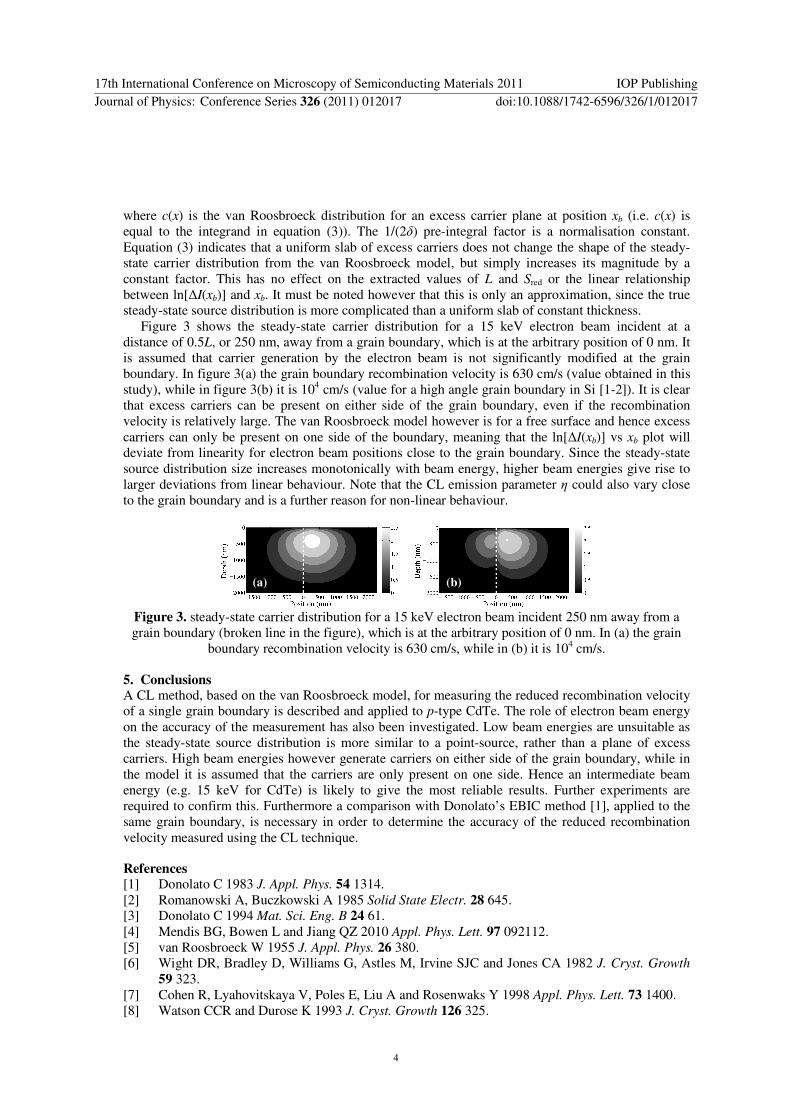
Figure 3 shows the steady-state carrier distribution for a 15 keV electron beam incident at a
distance of 05L or 250 nm away from a grain boundary which is at the arbitrary position of 0 nm It
is assumed that carrier generation by the electron beam is not significantly modified at the grain
boundary In figure 3(a) the grain boundary recombination velocity is 630 cms (value obtained in this
study) while in figure 3(b) it is 104 cms (value for a high angle grain boundary in Si [1-2]) It is clear
that excess carriers can be present on either side of the grain boundary even if the recombination
velocity is relatively large The van Roosbroeck model however is for a free surface and hence excess
carriers can only be present on one side of the boundary meaning that the ln[∆I(xb)] vs xb plot will
deviate from linearity for electron beam positions close to the grain boundary Since the steady-state
source distribution size increases monotonically with beam energy higher beam energies give rise to
larger deviations from linear behaviour Note that the CL emission parameter η could also vary close
to the grain boundary and is a further reason for non-linear behaviour
Figure 3 steady-state carrier distribution for a 15 keV electron beam incident 250 nm away from a
grain boundary (broken line in the figure) which is at the arbitrary position of 0 nm In (a) the grain
boundary recombination velocity is 630 cms while in (b) it is 104 cms
5 Conclusions A CL method based on the van Roosbroeck model for measuring the reduced recombination velocity
of a single grain boundary is described and applied to p-type CdTe The role of electron beam energy
on the accuracy of the measurement has also been investigated Low beam energies are unsuitable as
the steady-state source distribution is more similar to a point-source rather than a plane of excess
carriers High beam energies however generate carriers on either side of the grain boundary while in
the model it is assumed that the carriers are only present on one side Hence an intermediate beam
energy (eg 15 keV for CdTe) is likely to give the most reliable results Further experiments are
required to confirm this Furthermore a comparison with Donolatorsquos EBIC method [1] applied to the
same grain boundary is necessary in order to determine the accuracy of the reduced recombination
velocity measured using the CL technique
References [1] Donolato C 1983 J Appl Phys 54 1314
[2] Romanowski A Buczkowski A 1985 Solid State Electr 28 645
[3] Donolato C 1994 Mat Sci Eng B 24 61
[4] Mendis BG Bowen L and Jiang QZ 2010 Appl Phys Lett 97 092112
[5] van Roosbroeck W 1955 J Appl Phys 26 380
[6] Wight DR Bradley D Williams G Astles M Irvine SJC and Jones CA 1982 J Cryst Growth
59 323
[7] Cohen R Lyahovitskaya V Poles E Liu A and Rosenwaks Y 1998 Appl Phys Lett 73 1400
[8] Watson CCR and Durose K 1993 J Cryst Growth 126 325
(a) (b)
17th International Conference on Microscopy of Semiconducting Materials 2011 IOP PublishingJournal of Physics Conference Series 326 (2011) 012017 doi1010881742-65963261012017
4

Cathodoluminescence measurement of grain boundary
recombination velocity in vapour grown p-CdTe
B G Mendis and L Bowen
Department of Physics Durham University South Road Durham DH1 3LE UK
E-mail bgmendisdurhamacuk
Abstract A cathodoluminescence (CL) based method for measuring the minority carrier
diffusion length (L) and reduced recombination velocity (Sred) of an individual grain boundary
is presented The technique is based on the van Roosbroeck model for the steady-state carrier
distribution near a free surface in a semi-infinite solid Values of L = 055plusmn003 microm and
Sred = 023plusmn002 are obtained for vapour grown p-type CdTe The effect of the electron beam
generation volume on the accuracy of measurement is also discussed Intermediate beam
voltages (eg 15 kV for CdTe) are likely to produce the most reliable results The method can
be used to characterise the electrical activity of grain boundaries in thin-film solar cells
1 Introduction Grain boundaries have an important effect on the electrical properties of thin-film solar cells such as
CdTe and Cu(InGa)Se2 Charge is accumulated at the grain boundary due to the energy difference
between the quasi-neutrality level of the boundary and Fermi level in the bulk semiconductor The
built-in potential leads to band bending (upward bending for n-type semiconductors and downward
bending for p-type) such that majority carriers are repelled and minority carriers attracted towards the
boundary at a rate given by the recombination velocity where they undergo recombination Grain
boundaries with a high recombination velocity are sinks for minority carriers as well as strong barriers
for majority carrier flow and therefore reduce solar cell efficiency The electrical activity depends on
the nature of the grain boundary (eg coincident site lattice or random grain boundary)
Electron beam induced current (EBIC) has previously been used to measure the reduced
recombination velocity (ie the recombination velocity divided by the bulk diffusion velocity for
minority carriers) of individual grain boundaries in silicon [1-3] The reduced recombination velocity
is extracted from curve fitting of the raw data to non-analytic functions involving several material and
experimental parameters The electron beam generation volume is modeled using a simplified analytic
function (eg a spherically symmetric Gaussian [3]) The present authors however have developed a
cathodoluminescence (CL) method for measuring the reduced recombination velocity [4] based on the
van Roosbroeck [7] model for steady-state carrier distribution near a free surface The advantages of
this method are that it does not need any electrical contacts (cf EBIC) and the parameters of interest
are extracted directly from the experimental data without the need for curve fitting However the
electron beam generation volume is assumed to be a uniform plane parallel to the boundary which is
unrealistic In this paper the effect of the electron beam energy (and hence generation volume) on
accuracy of the CL measurement is discussed For completeness the theory behind the CL technique
and experimental data on p-type CdTe are also presented although a more detailed report on these
aspects can be found in [5]
17th International Conference on Microscopy of Semiconducting Materials 2011 IOP PublishingJournal of Physics Conference Series 326 (2011) 012017 doi1010881742-65963261012017
Published under licence by IOP Publishing Ltd 1
2 Background theory The van Roosbroeck model [5] describes the steady-state carrier distribution in a semi-infinite solid
containing a free surface Time independent uniform carrier generation in a plane parallel to and at a
distance xb from the free surface is assumed If a grain boundary is substituted for the free surface the
CL intensity I(xb) for an electron beam incident at position xb is
( )dx
L
xx
S
S
L
xxxkxI bb
b intinfin
+minus
+
minusminus
minusminus=
0red
red exp1
1exp)()( η (1)
where L is the minority carrier diffusion length Sred the reduced recombination velocity η the CL
emission efficiency and k a constant relating to CL detection efficiency The term within the square
brackets is the van Roosbroeck steady-state carrier distribution [5] ie it is assumed that the CL
intensity is directly proportional to the carrier density This assumption may be invalid for strongly
excitonic materials or at high injection levels but was experimentally verified for CdTe by
demonstrating a linear relationship between the CL intensity and electron beam current
If η is assumed to be independent of position x equation (1) simplifies as
( )[ ] ( )( )infin=
minus=∆minus
+=∆
b
bb
bb
xI
xIxI
L
x
S
SxI
)(1
1lnln
red
red (2)
A plot of ln[∆I(xb)] vs xb should therefore be a straight line The gradient of the straight line gives the
diffusion length L and the intercept gives the reduced recombination velocity Sred
3 Experimental procedure Panchromatic CL images were obtained from a ~70 microm thick p-type CdTe thin-film vapour grown on
a Ge substrate A Hitachi SU-70 scanning electron microscope (SEM) operating at 15 keV and 16 nA
beam current was used together with a Gatan MonoCL system for CL detection The pixel dwell time
for the panchromatic CL image was 300 micros ie significantly longer than the electron minority carrier
lifetime (τ) of 20 ns [6] thus ensuring steady-state conditions
2D Monte-Carlo simulations of the electron beam generation lsquovolumersquo were carried out using
screened Rutherford cross-sections and from this the steady-state minority carrier distribution in bulk
p-type CdTe was determined by solving the continuity equation using finite difference methods In
this paper we refer to this carrier distribution as the lsquosteady-state source distributionrsquo The simulation
parameters are L = 500 nm (section 41) τ = 20 ns [6] and 16 nA electron beam current A free
surface recombination velocity of 5x10⁵ cms [7] was applied as the boundary condition
4 Results and Discussion
41 Experimental data
Figure 1(a) shows a panchromatic CL image of a near end-on grain boundary in p-CdTe The intensity
normal to the grain boundary is extracted from the box region in figure 1(a) and is shown in figure
1(b) The intensity profile is used to plot a ln[∆I(xb)] vs xb graph (figure 1(c)) which shows overall
linear behavior except for data points closer to the grain boundary The deviation from linearity could
be due to variations in the CL emission parameter η at the grain boundary compared to the bulk (see
[6] for a more detailed discussion on the effects of η) A straight line was least squares fitted to figure
1(c) ignoring the first four data points closest to the grain boundary and values of L = 055 plusmn 003 microm
Sred = 023 plusmn 002 extracted from the gradient and intercept respectively The diffusion length L is
similar to values reported in the literature [9] Using τ = 20 ns [6] the measured values of L and Sred
give a recombination velocity of ~630 cms This is small compared to a 5x10⁵ cms recombination
velocity for a free surface in p-CdTe [7] or a value of ~104 cms for grain boundaries in Si [1-2]
However our observations as well as previous reports [8] indicate that vapour grown CdTe contains
low misorientation sub-grain boundaries which could explain the small recombination velocity
17th International Conference on Microscopy of Semiconducting Materials 2011 IOP PublishingJournal of Physics Conference Series 326 (2011) 012017 doi1010881742-65963261012017
2
Figure 1 (a) panchromatic CL image of a p-CdTe grain boundary (b) the intensity profile normal to
the grain boundary extracted from the box region in figure 1(a) and (c) the ln[∆I(xb)] vs xb plot
42 Numerical simulations
Although a near-linear relationship was observed between ln[∆I(xb)] and xb (figure 1(c)) carrier
generation by the electron beam needs to be analysed in more detail In the time independent van
Roosbroeck model uniform carrier generation in an infinite plane parallel to the grain boundary is
assumed Since the CL data are acquired under steady-state conditions the steady-state source
distribution (section 3) effectively provides the excess carriers Simulated steady-state source
distributions for 5 15 and 25 keV beam energies in p-CdTe are shown in figure 2 The spatial extent
of the steady-state source distribution increases with beam energy
Figure 2 steady-state source distribution for (a) 5 (b) 15 and (c) 25 keV electron beams in CdTe
Excess carriers are plotted on a logarithmic scale (note intensity scale for different figures)
The van Roosbroeck criterion of an infinite carrier generation plane clearly cannot be satisfied A
more reasonable criterion is that the dimensions of the steady-state source distribution must be at least
2L The full width at half maximum (FWHM) of the steady-state source distribution along a given
direction is arbitrarily defined as being the characteristic dimension along that direction Hence the
plots in figure 2 must have a FWHM of at least 2L along the vertical and horizontal axes For the 15
keV beam the FWHM is 820 and 1070 nm along the vertical and horizontal axes respectively (the
FWHM was calculated through the most intense region of the steady-state source distribution using a
linear scale for the excess carriers) Since L~500 nm (section 41) the steady-state source distribution
size is satisfactory for the 15 keV beam Beam energies below 15 keV (eg 5 keV) have steady-state
source distributions that are more point-like and are therefore unsuitable and vice-versa for beam
energies above 15 keV (eg 25 keV)
The symmetry of the plots in figure 2 about the vertical beam direction means that if the steady-
state source distribution is uniformly broadened by 2δ (δ geL) along the horizontal axis then the plane
of excess carriers in the van Roosbroeck model must be replaced by a uniform slab of thickness 2δ If
the slab is centred at the incident beam position xb the steady-state carrier distribution cprime(x) at distance
x from the boundary is obtained from superposition of the van Roosbroeck result over the entire slab
thickness ie
( ) ( )( )int
+
minus
=prime
+minus
+
minusminus
minusminus=prime
δ
δδ
δ
δ
b
b
x
x
bbb
L
Lxcxcdx
L
xx
S
S
L
xxxc
sinh)()(or exp
1
1exp
2
1)(
red
red (3)
(b) (c)
(a)
(a) (b) (c)
17th International Conference on Microscopy of Semiconducting Materials 2011 IOP PublishingJournal of Physics Conference Series 326 (2011) 012017 doi1010881742-65963261012017
3
where c(x) is the van Roosbroeck distribution for an excess carrier plane at position xb (ie c(x) is
equal to the integrand in equation (3)) The 1(2δ) pre-integral factor is a normalisation constant
Equation (3) indicates that a uniform slab of excess carriers does not change the shape of the steady-
state carrier distribution from the van Roosbroeck model but simply increases its magnitude by a
constant factor This has no effect on the extracted values of L and Sred or the linear relationship
between ln[∆I(xb)] and xb It must be noted however that this is only an approximation since the true
steady-state source distribution is more complicated than a uniform slab of constant thickness
Figure 3 shows the steady-state carrier distribution for a 15 keV electron beam incident at a
distance of 05L or 250 nm away from a grain boundary which is at the arbitrary position of 0 nm It
is assumed that carrier generation by the electron beam is not significantly modified at the grain
boundary In figure 3(a) the grain boundary recombination velocity is 630 cms (value obtained in this
study) while in figure 3(b) it is 104 cms (value for a high angle grain boundary in Si [1-2]) It is clear
that excess carriers can be present on either side of the grain boundary even if the recombination
velocity is relatively large The van Roosbroeck model however is for a free surface and hence excess
carriers can only be present on one side of the boundary meaning that the ln[∆I(xb)] vs xb plot will
deviate from linearity for electron beam positions close to the grain boundary Since the steady-state
source distribution size increases monotonically with beam energy higher beam energies give rise to
larger deviations from linear behaviour Note that the CL emission parameter η could also vary close
to the grain boundary and is a further reason for non-linear behaviour
Figure 3 steady-state carrier distribution for a 15 keV electron beam incident 250 nm away from a
grain boundary (broken line in the figure) which is at the arbitrary position of 0 nm In (a) the grain
boundary recombination velocity is 630 cms while in (b) it is 104 cms
5 Conclusions A CL method based on the van Roosbroeck model for measuring the reduced recombination velocity
of a single grain boundary is described and applied to p-type CdTe The role of electron beam energy
on the accuracy of the measurement has also been investigated Low beam energies are unsuitable as
the steady-state source distribution is more similar to a point-source rather than a plane of excess
carriers High beam energies however generate carriers on either side of the grain boundary while in
the model it is assumed that the carriers are only present on one side Hence an intermediate beam
energy (eg 15 keV for CdTe) is likely to give the most reliable results Further experiments are
required to confirm this Furthermore a comparison with Donolatorsquos EBIC method [1] applied to the
same grain boundary is necessary in order to determine the accuracy of the reduced recombination
velocity measured using the CL technique
References [1] Donolato C 1983 J Appl Phys 54 1314
[2] Romanowski A Buczkowski A 1985 Solid State Electr 28 645
[3] Donolato C 1994 Mat Sci Eng B 24 61
[4] Mendis BG Bowen L and Jiang QZ 2010 Appl Phys Lett 97 092112
[5] van Roosbroeck W 1955 J Appl Phys 26 380
[6] Wight DR Bradley D Williams G Astles M Irvine SJC and Jones CA 1982 J Cryst Growth
59 323
[7] Cohen R Lyahovitskaya V Poles E Liu A and Rosenwaks Y 1998 Appl Phys Lett 73 1400
[8] Watson CCR and Durose K 1993 J Cryst Growth 126 325
(a) (b)
17th International Conference on Microscopy of Semiconducting Materials 2011 IOP PublishingJournal of Physics Conference Series 326 (2011) 012017 doi1010881742-65963261012017
4