
Carrier Transport in PbS and PbSe QD Films Measured by ...
8
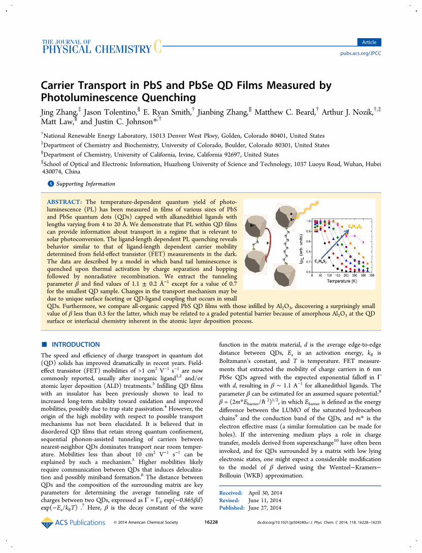
Carrier Transport in PbS and PbSe QD Films Measured by Photoluminescence Quenching Jing Zhang, ‡ Jason Tolentino, § E. Ryan Smith, † Jianbing Zhang, ∥ Matthew C. Beard, † Arthur J. Nozik, †,‡ Matt Law, § and Justin C. Johnson* ,† † National Renewable Energy Laboratory, 15013 Denver West Pkwy, Golden, Colorado 80401, United States ‡ Department of Chemistry and Biochemistry, University of Colorado, Boulder, Colorado 80301, United States § Department of Chemistry, University of California, Irvine, California 92697, United States ∥ School of Optical and Electronic Information, Huazhong University of Science and Technology, 1037 Luoyu Road, Wuhan, Hubei 430074, China * S Supporting Information ABSTRACT: The temperature-dependent quantum yield of photo- luminescence (PL) has been measured in films of various sizes of PbS and PbSe quantum dots (QDs) capped with alkanedithiol ligands with lengths varying from 4 to 20 Å. We demonstrate that PL within QD films can provide information about transport in a regime that is relevant to solar photoconversion. The ligand-length dependent PL quenching reveals behavior similar to that of ligand-length dependent carrier mobility determined from field-effect transistor (FET) measurements in the dark. The data are described by a model in which band tail luminescence is quenched upon thermal activation by charge separation and hopping followed by nonradiative recombination. We extract the tunneling parameter β and find values of 1.1 ± 0.2 Å −1 except for a value of 0.7 for the smallest QD sample. Changes in the transport mechanism may be due to unique surface faceting or QD-ligand coupling that occurs in small QDs. Furthermore, we compare all-organic capped PbS QD films with those infilled by Al 2 O 3 , discovering a surprisingly small value of β less than 0.3 for the latter, which may be related to a graded potential barrier because of amorphous Al 2 O 3 at the QD surface or interfacial chemistry inherent in the atomic layer deposition process. ■ INTRODUCTION The speed and efficiency of charge transport in quantum dot (QD) solids has improved dramatically in recent years. Field- effect transistor (FET) mobilities of >1 cm 2 V −1 s −1 are now commonly reported, usually after inorganic ligand 1,2 and/or atomic layer deposition (ALD) treatments. 3 Infilling QD films with an insulator has been previously shown to lead to increased long-term stability toward oxidation and improved mobilities, possibly due to trap state passivation. 4 However, the origin of the high mobility with respect to possible transport mechanisms has not been elucidated. It is believed that in disordered QD films that retain strong quantum confinement, sequential phonon-assisted tunneling of carriers between nearest-neighbor QDs dominates transport near room temper- ature. Mobilities less than about 10 cm 2 V −1 s −1 can be explained by such a mechanism. 5 Higher mobilities likely require communication between QDs that induces delocaliza- tion and possibly miniband formation. 6 The distance between QDs and the composition of the surrounding matrix are key parameters for determining the average tunneling rate of charges between two QDs, expressed as Γ = Γ 0 exp(−0.865βd) exp(−E a /k B T). 7 Here, β is the decay constant of the wave function in the matrix material, d is the average edge-to-edge distance between QDs, E a is an activation energy, k B is Boltzmann’s constant, and T is temperature. FET measure- ments that extracted the mobility of charge carriers in 6 nm PbSe QDs agreed with the expected exponential falloff in Γ with d, resulting in β ∼ 1.1 A −1 for alkanedithiol ligands. The parameter β can be estimated for an assumed square potential: 8 β = (2m*E barrier /ℏ 2 ) 1/2 , in which E barrier is defined as the energy difference between the LUMO of the saturated hydrocarbon chains 9 and the conduction band of the QDs, and m* is the electron effective mass (a similar formulation can be made for holes). If the intervening medium plays a role in charge transfer, models derived from superexchange 10 have often been invoked, and for QDs surrounded by a matrix with low lying electronic states, one might expect a considerable modification to the model of β derived using the Wentzel−Kramers− Brillouin (WKB) approximation. Received: April 30, 2014 Revised: June 11, 2014 Published: June 27, 2014 Article pubs.acs.org/JPCC © 2014 American Chemical Society 16228 dx.doi.org/10.1021/jp504240u | J. Phys. Chem. C 2014, 118, 16228−16235
Transcript of Carrier Transport in PbS and PbSe QD Films Measured by ...
Carrier Transport in PbS and PbSe QD Films Measured byPhotoluminescence QuenchingJing Zhang,‡ Jason Tolentino,§ E. Ryan Smith,† Jianbing Zhang,∥ Matthew C. Beard,† Arthur J. Nozik,†,‡
Matt Law,§ and Justin C. Johnson*,†
†National Renewable Energy Laboratory, 15013 Denver West Pkwy, Golden, Colorado 80401, United States‡Department of Chemistry and Biochemistry, University of Colorado, Boulder, Colorado 80301, United States§Department of Chemistry, University of California, Irvine, California 92697, United States∥School of Optical and Electronic Information, Huazhong University of Science and Technology, 1037 Luoyu Road, Wuhan, Hubei430074, China
*S Supporting Information
ABSTRACT: The temperature-dependent quantum yield of photo-luminescence (PL) has been measured in films of various sizes of PbSand PbSe quantum dots (QDs) capped with alkanedithiol ligands withlengths varying from 4 to 20 Å. We demonstrate that PL within QD filmscan provide information about transport in a regime that is relevant tosolar photoconversion. The ligand-length dependent PL quenching revealsbehavior similar to that of ligand-length dependent carrier mobilitydetermined from field-effect transistor (FET) measurements in the dark.The data are described by a model in which band tail luminescence isquenched upon thermal activation by charge separation and hoppingfollowed by nonradiative recombination. We extract the tunnelingparameter β and find values of 1.1 ± 0.2 Å−1 except for a value of 0.7for the smallest QD sample. Changes in the transport mechanism may bedue to unique surface faceting or QD-ligand coupling that occurs in smallQDs. Furthermore, we compare all-organic capped PbS QD films with those infilled by Al2O3, discovering a surprisingly smallvalue of β less than 0.3 for the latter, which may be related to a graded potential barrier because of amorphous Al2O3 at the QDsurface or interfacial chemistry inherent in the atomic layer deposition process.
■ INTRODUCTION
The speed and efficiency of charge transport in quantum dot(QD) solids has improved dramatically in recent years. Field-effect transistor (FET) mobilities of >1 cm2 V−1 s−1 are nowcommonly reported, usually after inorganic ligand1,2 and/oratomic layer deposition (ALD) treatments.3 Infilling QD filmswith an insulator has been previously shown to lead toincreased long-term stability toward oxidation and improvedmobilities, possibly due to trap state passivation.4 However, theorigin of the high mobility with respect to possible transportmechanisms has not been elucidated. It is believed that indisordered QD films that retain strong quantum confinement,sequential phonon-assisted tunneling of carriers betweennearest-neighbor QDs dominates transport near room temper-ature. Mobilities less than about 10 cm2 V−1 s−1 can beexplained by such a mechanism.5 Higher mobilities likelyrequire communication between QDs that induces delocaliza-tion and possibly miniband formation.6 The distance betweenQDs and the composition of the surrounding matrix are keyparameters for determining the average tunneling rate ofcharges between two QDs, expressed as Γ = Γ0 exp(−0.865βd)exp(−Ea/kBT) .7 Here, β is the decay constant of the wave
function in the matrix material, d is the average edge-to-edgedistance between QDs, Ea is an activation energy, kB isBoltzmann’s constant, and T is temperature. FET measure-ments that extracted the mobility of charge carriers in 6 nmPbSe QDs agreed with the expected exponential falloff in Γwith d, resulting in β ∼ 1.1 A−1 for alkanedithiol ligands. Theparameter β can be estimated for an assumed square potential:8
β = (2m*Ebarrier/ℏ2)1/2, in which Ebarrier is defined as the energy
difference between the LUMO of the saturated hydrocarbonchains9 and the conduction band of the QDs, and m* is theelectron effective mass (a similar formulation can be made forholes). If the intervening medium plays a role in chargetransfer, models derived from superexchange10 have often beeninvoked, and for QDs surrounded by a matrix with low lyingelectronic states, one might expect a considerable modificationto the model of β derived using the Wentzel−Kramers−Brillouin (WKB) approximation.
Received: April 30, 2014Revised: June 11, 2014Published: June 27, 2014
Article
pubs.acs.org/JPCC
© 2014 American Chemical Society 16228 dx.doi.org/10.1021/jp504240u | J. Phys. Chem. C 2014, 118, 16228−16235

While providing a measure of carrier mobility, FETmeasurements generally probe only 1−2 monolayers of QDsnear the gate electrode and may be insensitive to trap statesthat become occupied upon gate biasing. Thus, complementarymeasurements of β that can be made under weak lightexcitation and little or no bias to ensure that occupation ofelectronic states throughout the bulk of the film is similar tothat in a photovoltaic device would provide valuable newinformation. Photoluminescence (PL) of colloidal QDs is oftenused as an indicator of sample quality, and can usually beinterpreted as radiative electron−hole (quantum-confinedexciton) recombination when QDs are electronically isolatedfrom each other.11 Charge traps and resulting trapping/detrapping dynamics can play a significant role in carriertransport, especially for samples with surface states.12,13 Surfacestates resulting from nonstoichiometry due to lattice termi-nation have been characterized by their temperature-dependentPL, and their influence can be modulated by changing thecomposition of the QD surface via ligand exchange.14 Defectstates that result in nonradiative recombination centers can alsobe inferred via the temperature-dependent PL quenching thatoccurs as carriers overcome barriers to reach “dark”recombination centers through thermal activation. In QDfilms with relatively short organic or inorganic ligands, thedominant form of PL quenching is electron−hole separationand charge diffusion followed by nonradiative recombination.15
In previous work, we interpreted size- and temperature-dependent PL quenching in terms of an exponential band tailmodel,16 which faithfully reproduced both PL intensities andspectral profiles for films of PbS QDs capped with short ligands.In this model, photoexcited charges quickly relax to the bandtail, where the charges are localized. They remain localized atlow temperatures and recombine radiatively from the bottom ofthe density of states. At higher temperatures, the carriers can beactivated in an Arrhenius fashion to states higher in the bandtail that are delocalized, such that multiple trapping/detrappingevents proceed, resulting in hopping transport. The energydemarcation between localization and delocalization, some-times referred to as the mobility edge,17,18 can be changed byQD size, ligands, and temperature, which redistributeselectrons/holes within these states. Here we extend ourprevious work to make a direct connection between PL andcharge transport by employing a series of ligands that increasesthe interdot distance but retains a consistent QD/ligandchemistry (i.e., thiolates) and matrix identity (i.e., alkanes). Weshow that the Arrhenius prefactor can be related in a simpleway to the distance-dependent carrier tunneling rate.Although demonstrations of high mobility and investigations
of the transport mechanism in lead chalcogenide QD films havebeen carried out mostly on QDs with diameter greater than 5nm, the most efficient QD solar cells have been fabricated fromQDs with band gaps greater than 1 eV and confinementenergies in excess of 0.5 eV,19 corresponding to QD diameters< 4 nm. With a greater HOMO−LUMO splitting, the lowestexciton levels for small QDs are closer to electronic resonancewith the surrounding matrix (e.g., the tunneling barrier issmaller). A close comparison with first-principles calculations isalso possible with smaller QDs due to the lower computationalcost of treating the necessary number of atoms.
■ EXPERIMENTAL METHODSSample Preparation. PbS and PbSe QDs were synthesized
according to Hines et al.20 and Yu et al.,21 respectively, and kept
air-free throughout synthesis, washing, and experiments. Thefilms were either spin-cast in the case of untreated films (oleate-capped) or dip-coated from 1 mM solutions of the particularalkanedithiol in acetonitrile. The number of dipping cyclesvaried with the ligand from about 15 to about 30. The QDdipping solution was hexane and contained roughly 20 mg/mLof QDs. The optical density at the lowest exciton peak wastypically 0.1. Sapphire was used as a substrate due to itssuperior infrared transmission and high thermal conductivity,although experiments performed with films cast on glassproduced similar results. Absorption spectra were collected on aShimadzu UV−vis−NIR spectrometer. The half-width at half-maximum OD was recorded for the lowest exciton absorptionsince for the smallest QD samples the full width was notresolved.
Photoluminescence Measurements. PL quantum yieldmeasurements were performed on drop-cast films in anintegrating sphere with either a 750 or 840 nm light-emittingdiode as the excitation source and a cooled InGaAs photodiodeas the detector. The films were air exposed for a few minutesduring the experiment, but the ΦPL for untreated PbS QDs wasfound to be stable during that period.For temperature-dependent PL experiments, the 2 mm thick
substrates were sealed in a 1 in diameter Cu holder with a Vitono-ring sandwiched between the substrate with the QD film anda blank sapphire substrate. The holder was sealed in the Heglovebox and placed in a closed loop He flow cryostat (18−325K) fitted with sapphire windows that was evacuated to 1 × 10⁻⁴
Torr. The sample was cooled to 18 K and then heated slowly in20 K steps, with an equilibration time of 10 min at eachtemperature. Collecting PL spectra during cooling instead ofheating produced the same results. The 514 nm line of an Ar-ion laser was used to excite the sample, with a beam size ofapproximately 2.5 mm and power roughly 30 mW. Eachspectrum required roughly 1 min of exposure time. Experi-ments on some samples were performed at several powers (upto 100 mW) with no clear change in PL quenching behavior.The excitation beam was modulated at 500 Hz, and the sampleemission was routed through a monochromator with a 300groove/mm grating blazed at 1250 nm. A dual, balanced Gephotodiode was used in concert with a lock-in amplifier todetect the signal. The spectral sensitivity of the entire systemwas determined with a calibrated tungsten lamp, and PL spectrawere corrected accordingly.
Atomic Layer Deposition. For atomic layer depositioninfilling and overcoating, amorphous Al2O3 was deposited in ahomemade continuous wave ALD system inside a gloveboxusing trimethylaluminum (TMA) and water (H2O) at asubstrate temperature of 27 °C and an operating pressure of84−87 mTorr. Pulse and purge times for TMA were 20 ms and60 s, respectively. Pulse and purge times for H2O were 40 msand 120 s, respectively.
Fabrication of QD Films for Field-Effect Measure-ments and Atomic Layer Deposition Infilling. PbS NCfilms were dip coated in a layer-by-layer fashion with amechanical dip coater mounted inside an air-free glovebox. Thesubstrates (prepatterned FET substrates or sapphire), cleanedby sonication in acetone and isopropanol, were dipped into a 2mg mL−1 solution of QDs in dry hexane and then a 1 mMsolution of the appropriate alkanedithiols in dry acetonitrile.We fabricated films with thicknesses in the range of 30−100 nm(thin for FETs and thicker for PL).
The Journal of Physical Chemistry C Article
dx.doi.org/10.1021/jp504240u | J. Phys. Chem. C 2014, 118, 16228−1623516229

■ RESULTS AND DISCUSSIONIn Figure 1 we show PL spectra versus temperature (18−325K) for films of 3.8 nm PbS QDs treated with 1,2-ethanedithiol
(EDT, Figure 1a), 1,4-butanedithiol (BuDT, Figure 1b), or 1,8-octanedithiol (ODT, Figure 1c). For EDT-treated films, aninitial red shift is observed as the temperature is raised,consistent with activation of carriers into states closer to themobility edge such that PL only arises from carriers that residedeeper in the band tails. The blue shift seen at highertemperatures is assigned to band gap widening for PbS22
accounting for ∼20 meV of the shift15 and redistribution ofcarriers to higher energy states responsible for the remainder.The blue shift occurs throughout the temperature range but isonly evident at high temperatures when the deeper band tail
emission is strongly quenched. The PL from ligand-exchangedsamples was often too low to be quantified at roomtemperature, where absolute ΦPL measurements were per-formed. Thus, ΦPL of an oleate-capped QD film of each sizewas determined in an integrating sphere at 295 K, followed by ameasurement of a reference spectrum collected in thetemperature-dependent PL apparatus. The reference spectrumat room temperature was compared with spectra obtained fromligand-exchanged films at lower temperatures where emissionwas measurable in order to estimate ΦPL at low temperature.For PbSe QDs, the measured variation in ΦPL was
considerably larger than for PbS QDs, likely due to theparticular sensitivity of PbSe to surface oxidation,12,23 which canoccur in the few minutes necessary to perform the integratingsphere measurements. We therefore could not reliably quantifyintegrated PL versus temperature for PbSe on an absolute scale.For PbS QDs at 18 K, ΦPL is similar to that of uncoupled QDsin solution: 2−40% depending on QD size and ligand length(Table 1), which is calculated assuming length of 1.25 Å per sp3
C−C bond (1.54 Å bond length and tetrahedral angle of109.5°). ΦPL increases for smaller oleate-capped QDs,consistent with previous results that were explained by theenergy dependence of likely nonradiative transitions, includingboth trapping in deep levels and energy transfer to ligands.24,25
Figure 2 displays the integrated PL intensity and peak energyversus ligand treatment and temperature for films of 2.9 nmPbS QDs (Figure 2a,b) and 2.5 nm PbSe QDs (Figure 2c,d).The behavior of PbS and PbSe QDs is qualitatively similar.There is an initial red shift with increasing temperature with amagnitude depending on ligand length−shorter ligands have alarger shift. The red shift is also QD size-dependent: ∼50 meVfor 2.9 nm (Figure 2a) and ∼10 meV for 3.8 nm PbS QDsexchanged with EDT (Figure 1a). Concomitant with thereduction in red shift with increased QD size is a lowering ofthe temperature at which 50% PL quenching occurs, from 150K for 2.3 nm PbS QDs capped with EDT (data not shown) to50 K for the corresponding 3.8 nm QD film (Figure 1a). As theemission becomes strongly quenched at higher temperatures,the PL peak blueshifts by up to ∼80 meV from its minimumvalue to the position at room temperature.In order to analyze the data in more detail, we derive a
kinetic model that accounts for the expected routes of decay ofthe photoexcited carriers, including (1) radiative recombination
Figure 1. PL spectra for 3.8 nm PbS QD films treated with (a) EDT,(b) BuDT, or (c) ODT.
Table 1. ΦPL for Various PbS QD Films at 18 K
treatment
nominal ligandlength/
angstroms2.3 nmΦPL
2.9nmΦPL
3.8 nmΦPL
3.8 nm +ALD ΦPL
none (oleic acidcapped)
19.70 0.36 0.30 0.18 --
1,2-ethanedithiol(EDT)
4.25 0.039 0.11 0.021 0.016
1,3-propanedithiol(PrDT)
5.50 0.080 0.04 0.022 0.0031
1,4-butanedithiol(BuDT)
6.75 0.13 0.22 0.019 --
1,5-pentanedithiol(PeDT)
8.00 0.28 0.36 0.054 --
1,6-hexanedithiol(HDT)
9.25 0.29 0.37 0.074 0.03
1,8-octanedithiol(ODT)
11.75 0.32 0.36 0.13 --
The Journal of Physical Chemistry C Article
dx.doi.org/10.1021/jp504240u | J. Phys. Chem. C 2014, 118, 16228−1623516230

from the bottom of the band; (2) nonradiative decay associatedwith carriers localized in individual QDs; and (3) carrierseparation and diffusion leading to nonradiative decay atrecombination sites. If we assume for simplicity that each of therates is linear in light intensity, then ΦPL can be described interms of competing radiative and nonradiative processes:26
Φ =+ ∑
Tk
k k( )PL
RR
RR NR (1)
where kRR is the radiative recombination rate constant(corresponding to process (1)) and ΣkNR is the sum of variousnonradiative recombination rate constants that in the followingdiscussion we separate into temperature-independent (kNR,process 2), and temperature-dependent (kCT, process 3). Asdiscussed above, when d is reduced, the PL quenching occurs ata lower temperature, which is consistent with diffusion-limitedrecombination. The most general form of the temperature-dependent hopping rate constant is
α= − ∗⎜ ⎟⎛⎝⎜
⎛⎝
⎞⎠
⎞⎠⎟k T
TT
( ) expv
CT(2)
which includes an attempt frequency α, an exponent v, and acharacteristic temperature T*. When v = 1, the nearest-neighbor hopping (NNH) transport regime is active, and T* isexpressed as an activation energy Ea. When v = 0.5, the Efros−Shklovskii variable range hopping (ES VRH) transportmechanism is dominant, while for v = 0.25 the Mott VRHregime applies.7 The PL data sets do not afford adequate signal-to-noise ratios to determine the transport regime unequivocally.We assume that NNH is primarily responsible for the PLquenching, and further discussion of transport regimes can befound in the Supporting Information. We also assume that PLquenching is dominated by minority carriers (electrons) since
previous studies have revealed p-type behavior for thiolate-capped PbS and PbSe QD films.27
With the additional assumption that kRR is not stronglytemperature dependent,28 ΦPL becomes
Φ =+ +
=+ +α −
Tk
k k T k
e k k
( )( )
1
1 /k
PLRR
RR CT NR
( )NR RR
Ek T
RR
aB
(3)
An example of a fit of eq 3 to the ΦPL(T) data is shown inFigure 3 for 2.9 nm PbS QDs in various films.In order to reduce the number of free parameters in fits with
eq 3, we explored making some variables global in data sets ofthe same QD size but different length ligand. Fits in which Eawas made global among all ΦPL(T) curves were superior to fitsin which α was a global variable (Figure S1). This is mostclearly seen for large d in which the curvature of IPL(T) near the
Figure 2. PL peak position and integrated PL intensity for (a,b) 2.9 nm PbS QDs and (c,d) 2.5 nm PbSe QDs.
Figure 3. Simultaneous fit of eq 3 of temperature-dependent PL forfilms of 2.9 nm PbS QDs following alkanedithiol treatments.
The Journal of Physical Chemistry C Article
dx.doi.org/10.1021/jp504240u | J. Phys. Chem. C 2014, 118, 16228−1623516231

quenching temperature is noticeably reduced, which can onlybe fitted properly if α changes with d. When Ea and α were bothallowed to vary, the dependence of α on ligand length wasretained while there was no trend for Ea. If the Coulombcharging energy EC were to dictate the dependence of Ea on d,then Ea ∝ d‑1, but the lack of a clear dependence implies that ECis not the primary source of the potential barrier to hopping inthese samples. Table 2 displays various fitted and calculatedparameters for three sets of PbS QD samples. Here we haveassumed a kRR value of 3 × 10⁵ s−1.29 The value of kNR is shownonly for EDT capping but scales according to ΦPL (18K) forother ligands (Figure S3). Similar data for the PbSe QDsamples are found in Table S1 and Figure S2.We connect the prefactor α in ΦPL(T) to the first term in the
Miller−Abrahams equation30 also used for determination of βfrom FET measurements:9
α ∝ β−e d0.865 (4)
Plots of α versus d on a semilog scale for the two larger PbSQD sizes (Figure 4a,b) reveal approximately linear trends withextracted β values ∼1 Å−1, similar to FET results.9 There aresmall deviations from linearity through the alkanedithiol series,which likely arise from the assumption that the interparticlespacing d is equal to the calculated ligand length. Ligandconformations that allow for bidentate binding31 or varyingdegrees of interdigitation could give rise to the nonlinearity,which has been observed in other determinations of β fortreated QD films9,15 and in molecular conductance studies thatemployed alkanedithiol ligands.32 The maximum pre-exponen-tial factor α0 (α extrapolated to d = 0) is ∼1× 10¹² s−1, 1× 10¹³
s−1, and 3× 10¹² s−1 for 3.8, 2.9, and 2.3 nm PbS QDs,respectively. Using α values for EDT-exchanged films in theEinstein−Smoluchowski relation (μ = (e/2kT)d2α) results inmobilities ranging from 5 × 10⁻⁴ to 4 × 10⁻² cm2 V−1 s−1 atroom temperature, consistent with the magnitude of electronmobilities determined by FET measurements performed onsimilar films (Figure S4).For 2.2 nm PbS QD films (Figure 4c), full PL quenching
does not occur until at or above room temperature for ligandslonger than BuDT, and heating above 325 K was notperformed since film rearrangement or sintering may produce
uncontrolled effects on the PL signal. Further uncertainty arisesfrom the fact that the IPL(T) curves have a peak at intermediatetemperatures for smaller QDs, especially for longer ligands.Thus, we restricted our analysis to EDT, PrDT, and BuDT forthis QD size, which gives β ∼ 0.7 Å−1. For QDs with diameterslarger than 4 nm, the PL was too weak for a proper analysis,thus it was not possible to determine a value of β.In Figure 5 are shown normalized ΦPL(T) curves for 3.8 nm
PbS QD films infilled with Al2O3.33 The quenching behavior
remains essentially the same for each of the three differentlength ligand treatments. The ΦPL values at 18 K (Table 1) aresignificantly smaller than those observed for non-ALD infilledfilms, suggesting surface chemistry that enhances kNR or morefacile charge separation at low temperature. The data werefitted with eq 3 and the resulting α versus d trend is shown inthe inset.Unlike in high-quality bulk semiconductors,34 the room
temperature PL for high-mobility QD films at open circuit islow due to the dominance of nonradiative over radiativerecombination. Thus, the most informative aspect of thesteady-state PL from coupled QD films is its temperaturedependence, rather than the absolute value of ΦPL at roomtemperature. However, relatively high values of ΦPL at lowtemperature and the trend with ligand length prove that the PL
Table 2. Lowest Exciton Peak Room Temperature Absorption Width (fwhmabs), PL Peak Width (fwhmPL) at 18K, Site EnergyDisorder (ED), Coulomb Charging Energy (EC), and Best-Fit Values of β, kNR, and Ea for Three PbS QD Filmsa
peak abs/eV fwhmabs/eV fwhmPL/eV ED/meV EC/meV Ea/meV (v = 1) kNR (sec−1) β/Å−1
1.69 266 185 112 63 96 3.5 × 10⁶ 0.7 ± 0.061.39 154 145 66 45 127 6.1 × 10⁶ 1.1 ± 0.181.12 132 90 56 27 34 1.5 × 10⁷ 0.9 ± 0.08
aEC, FWHMPL, and kNR are determined for EDT capping.
Figure 4. Frequency factor α versus QD separation for 3.8 and 2.9, and 2.3 nm PbS QDs films.
Figure 5. PL of Al2O3-infilled 3.8 nm PbS QD film previously treatedwith alkanedithiols. ΦPL is normalized to unity at 18 K for each sample.Inset: α vs ligand length.
The Journal of Physical Chemistry C Article
dx.doi.org/10.1021/jp504240u | J. Phys. Chem. C 2014, 118, 16228−1623516232

is not emitted from a small subset of QDs disconnected fromthe relevant events of charge separation and diffusion. Thetrend of larger ΦPL with smaller QD size has been previouslyobserved in solution and discussed in terms of the energy gaplaw that dictates nonradiative decay rates, which should also berelevant here.24 Surface faceting and stoichiometry areadditional size-dependent effects that could influence ΦPL.
35,14
The amount of surface chalcogen increases for larger QDs36
and has been previously implicated in poor emission yields ofCdSe and PbSe.37,38 The trend of lower ΦPL with decreasedligand length at low temperature (Table 1) likely results fromtwo factors: (1) a different ligand packing geometry leading toincreased density of QD-ligand bonds and a higher surfaceanion content, or (2) an increase in interdot coupling thatfacilitates exciton dissociation with minimal thermal activation.The trend of ΦPL versus d at 18 K matches that of the PL peakshift with d (Figure S3), which suggests that interdot couplinginferred from PL red-shifting is a dominant factor.Although the barrier height Ebarrier to carrier tunneling is
primarily determined by the electronic structure of the matrix,the activation energy Ea is affected by other factors. Intemperature-dependent dark conductivity measurements, Eahas been asserted to depend on the distribution of lowestexciton energies in the QD ensemble and/or the Coulombcharging energy EC for charge transfer between QDs.39 Thefwhmabs, of the lowest exciton absorption, which is one measureof energy disorder, varies significantly through our sampleseries (Table 2). The site energy disorder, ED in Table 2 andTable S1, is calculated using ED = fwhmabs/2(2 ln 2)
1/2, which isthe standard deviation of the Gaussian distribution of lowestexciton energies. We find at best a weak correlation betweenthe size-dependent trends of ED and Ea. The Coulomb chargingenergy EC should be proportional to 1/diameter, and we showin Table 2 calculated values using the formalism as in ref 9. Themagnitude of EC is smaller than that of ED but coincidentallyfollows a similar trend. The lack of a clear dependence of Ea ond in the fits suggests that the contribution from EC is minor.Other QD size-dependent contributions to Ea could includeincreasing bond length disorder due to changing surface tovolume ratio and a higher degree of “charging” (i.e., long-livedtrapped carriers) due to the presence of higher energy facets,both of which could deepen the band tail and increase Ea.
40
Ligand phase transitions were also previously asserted to play arole in temperature-dependent quenching behavior, whichwould potentially modulate Ea.
41
β measured by PL quenching is 1.1 ± 0.2 Å−1 for the twolarger PbS and PbSe QD samples, in agreement with measuredFET mobility vs ligand length for PbSe QDs for both theelectron and the hole. The lower β value of ∼0.7 Å−1 for thesmallest PbS QD sample implies a size-dependent barrier forcarrier tunneling. The very large confinement energy (>1 eV)for the smallest QDs could have consequences for both Ebarrierand the probability of mixing between QD and ligand states.The additional 0.3 eV in confinement energy for the 2.3 nmQDs will result mostly in a rise in the conduction bandedge,42,43 although unless the barrier for the larger QDs issignificantly less than the 1.6 eV previously estimated, the effectcannot account for such a large decrease in β.The possibility of increased interaction between band edge
states and ligand orbitals is intriguing but difficult to test. Theeffect of mixing may be to smooth the abrupt square potentialbarrier that is assumed in the WKB model of β.44 Relatively fastcharge transfer from PbS and PbSe QDs to ligands is well-
established;45−47 however, in most cases the acceptor isdesigned to capture charge rather than serve as a conduitbetween QDs. It was suggested that the reason for theanomalously low 1.6 eV barrier for carrier tunneling in PbSeQDs capped with alkanethiols was QD-ligand mixing.9 For thatsize, the confinement energy was only 0.4 eV, ∼1 eV smallerthan that of the PbS QDs studied here. Thus, if mixing occursfor larger QDs, it is likely to be much stronger for smaller QDswhose lowest exciton levels are closer to resonance with ligandlevels. Measurements of transient photoconductivity performedon films composed of PbSe QDs treated with different lengthalkyldiamines revealed β of 0.57 A−1.48 Mixing with ligandstates was suggested as a reason for the lower than expected βvalue, but no definitive conclusions were drawn. Through time-resolved PL measurements Choi et al. also reported a relativelylow value of β = 0.26 A−1 for PbS QDs capped with dithiols,although the linker chains consisted of benzene units ratherthan saturated chains.49 More recently, Scheele et al. claimed aresonant alignment between the valence band of 9.8 nm PbSQDs and a tetrathifulvalenetetracarboxylate ligand.50 Anom-alously high FET mobilites for the measured interdot spacing aswell as XPS data and atomistic calculations supported thenotion that transport was ligand-assisted. Tailored inorganicligands were not employed here, but are even more likely toserve as active participants in charge transport.1,51
Since surface faceting changes with QD size, it is possiblethat interactions between specific facets are more stronglyengendered for small QDs. For example, it has been shownthrough DFT calculations52 that when coupling occurs via the(111) facet, which becomes more dominant in small PbS orPbSe QDs, the coupling energy is attenuated more weakly withinterdot spacing than similar coupling via the (100) facet. LocalQD alignment along the (111) facets, or even some degree ofnecking, may facilitate the lower barrier to charge transfer.PbS QD films infilled with alumina exhibit increased electron
FET mobility (from ∼10−3 to ∼10−2 cm2 V−1 s−1 for EDTtreated QDs, Figure S4) compared with noninfilled films, but aβ of less than 0.3. The similar IPL(T) profiles after ALD suggestthat PL quenching occurs by the same mechanism as innoninfilled films. If the expression β = (2m*Ebarrier/ℏ
2)1/2 holds,the much smaller value of β for alumina-infilled films wouldsuggest an order of magnitude decrease in the product of thetunneling barrier height and the carrier effective mass.However, the large band gap of crystalline Al2O3 (∼6 eV)should result in Ebarrier greater than 2 eV and thus not muchsmaller than that of the alkanedithiols, which also exhibitedEbarrier ∼ 2 eV. Moreover, studies of ALD coating of Al2O3 onTiO2 or SnO2 revealed a β of about 1 Å−1 for electrontunneling, with a barrier height similar to that expected for PbSQDs.53 One possibility is that amorphous Al2O3 material, with aband gap of 2.6−2.9 eV,54 is formed at the surface of the QDsand may serve to smooth the potential barrier. Possible surfacechemistry modifications including surface doping after ALDmay also influence β but have not been studied systematically.
■ CONCLUSIONSWe have shown a clear correlation between PL quenching andpreviously reported field-effect mobility measurements for QDfilms with varying inter-QD spacing. For relatively large PbSQDs (diameter >2.5 nm), the data can be fitted with a model inwhich charge carriers tunnel between states on weakly coupledQDs with β ∼ 1. For smaller QDs, the value of β is reduced,possibly due to effects related to the interaction between
The Journal of Physical Chemistry C Article
dx.doi.org/10.1021/jp504240u | J. Phys. Chem. C 2014, 118, 16228−1623516233

particular surface facets or mixing with ligand states due to thelarge confinement energy. Alumina-infilled 3.8 nm PbS QDfilms exhibit an unusually small β, which cannot be explainedsolely by the expected change in barrier height for crystallineAl2O3 compared with alkanedithiols. Our results show thatutilizing steady-state PL to determine barriers to chargetransport on QD films intended for solar photoconversioncan reveal important trends that may complement informationfrom electrical measurements.
■ ASSOCIATED CONTENT*S Supporting InformationDiscussion of transport regime, additional global fittinginformation, PL data and analysis for PbSe QDs, PL quantumyield and peak shift correlation, and FET measurements. Thismaterial is available free of charge via the Internet at http://pubs.acs.org.
■ AUTHOR INFORMATIONCorresponding Author*Mailing address: NREL, 15013 Denver West Pkwy, Golden,CO 80401. Phone: 303-384-6190; e-mail: [email protected].
NotesThe authors declare no competing financial interest.
■ ACKNOWLEDGMENTSThe authors gratefully acknowledge the Center for AdvancedSolar Photophysics (CASP), an Energy Frontier ResearchCenter sponsored by Basic Energy Sciences, U.S. Departmentof Energy. J.T. acknowledges support from an NSF GraduateResearch Fellowship.
■ REFERENCES(1) Lee, J. S.; Kovalenko, M. V.; Huang, J.; Chung, D. S.; Talapin, D.V. Band-Like Transport, High Electron Mobility and High Photo-conductivity in All-Inorganic Nanocrystal Arrays. Nat. Nanotechnol.2011, 6, 348−352.(2) Choi, J. H.; Fafarman, A. T.; Oh, S. J.; Ko, D. K.; Kim, D. K.;Diroll, B. T.; Muramoto, S.; Gillen, J. G.; Murray, C. B.; Kagan, C. R.Bandlike Transport in Strongly Coupled and Doped Quantum DotSolids: A Route to High-Performance Thin-Film Electronics. NanoLett. 2012, 12, 2631−2638.(3) Liu, Y.; Tolentino, J.; Gibbs, M.; Ihly, R.; Perkins, C. L.; Liu, Y.;Crawford, N.; Hemminger, J. C.; Law, M. PbSe Quantum Dot Field-Effect Transistors with Air-Stable Electron Mobilities above 7 cm2 V−1
s−1. Nano Lett. 2013, 13, 1578−1587.(4) Liu, Y.; Gibbs, M.; Perkins, C. L.; Tolentino, J.; Zarghami, M. H.;Bustamante, J.; Law, M. Robust, Functional Nanocrystal Solids byInfilling with Atomic Layer Deposition. Nano Lett. 2011, 11, 5349−5355.(5) Shabaev, A.; Efros, A. L.; Efros, A. L. Dark and Photo-Conductivity in Ordered Array of Nanocrystals. Nano Lett. 2013, 13,5454−5461.(6) Nozik, A. J. Spectroscopy and Hot Electron Relaxation Dynamicsin Semiconductor Quantum Wells and Quantum Dots. Annu. Rev.Phys. Chem. 2001, 52, 193−231.(7) Shklovskiĭ, B. I.; Efros, A. L. Electronic Properties of DopedSemiconductors; Springer-Verlag: Berlin/New York, 1984.(8) Gurney, R. W.; Condon, E. U. Phys. Rev. 1929, 33, 127−140.(9) Liu, Y.; Gibbs, M.; Puthussery, J.; Gaik, S.; Ihly, R.; Hillhouse, H.W.; Law, M. Dependence of Carrier Mobility on Nanocrystal Size andLigand Length in PbSe Nanocrystal Solids. Nano Lett. 2010, 10,1960−1969.
(10) Gray, H. B.; Winkler, J. R. Long-Range Electron Transfer. Proc.Natl. Acad. Sci. U.S.A. 2005, 102, 3534−3539.(11) Dabbousi, B. O.; RodriguezViejo, J.; Mikulec, F. V.; Heine, J. R.;Mattoussi, H.; Ober, R.; Jensen, K. F.; Bawendi, M. G. (CdSe)ZnSCore-Shell Quantum Dots: Synthesis and Characterization of a SizeSeries of Highly Luminescent Nanocrystallites. J. Phys. Chem. B 1997,101, 9463−9475.(12) Chappell, H. E.; Hughes, B. K.; Beard, M. C.; Nozik, A. J.;Johnson, J. C. Emission Quenching in PbSe Quantum Dot Arrays byShort-Term Air Exposure. J. Phys. Chem. Lett. 2011, 2, 889−893.(13) Nagpal, P.; Klimov, V. I. Role of Mid-Gap States in ChargeTransport and Photoconductivity in Semiconductor NanocrystalFilms. Nat. Commun. 2011, 2, 486.(14) Hughes, B. K.; Ruddy, D. A.; Blackburn, J. L.; Smith, D. K.;Bergren, M. R.; Nozik, A. J.; Johnson, J. C.; Beard, M. C. Control ofPbSe Quantum Dot Surface Chemistry and Photophysics Using anAlkylselenide Ligand. ACS Nano 2012, 6, 5498−5506.(15) Gao, J. B.; Johnson, J. C. Charge Trapping in Bright and DarkStates of Coupled PbS Quantum Dot Films. ACS Nano 2012, 6,3292−3303.(16) Tsang, C.; Street, R. A. Recombination in Plasma-DepositedAmorphous Si−H - Luminescence Decay. Phys. Rev. B 1979, 19,3027−3040.(17) Werner, J.; Peisl, M. Exponential Band Tails in PolycrystallineSemiconductor Films. Phys. Rev. B 1985, 31, 6881−6883.(18) Mott, N. The Mobility Edge since 1967. J. Phys. C 1987, 20,3075−3102.(19) Maraghechi, P.; et al. The Donor-Supply Electrode EnhancesPerformance in Colloidal Quantum Dot Solar Cells. ACS Nano 2013,7, 6111−6116.(20) Hines, M. A.; Scholes, G. D. Colloidal PbS Nanocrystals withSize-Tunable Near-Infrared Emission: Observation of Post-SynthesisSelf-Narrowing of the Particle Size Distribution. Adv. Mater. 2003, 15,1844−1849.(21) Yu, W. W.; Falkner, J. C.; Shih, B. S.; Colvin, V. L. Preparationand Characterization of Monodisperse PbSe Semiconductor Nano-crystals in a Noncoordinating Solvent. Chem. Mater. 2004, 16, 3318−3322.(22) Olkhovets, A.; Hsu, R. C.; Lipovskii, A.; Wise, F. W. Size-Dependent Temperature Variation of the Energy Gap in Lead-SaltQuantum Dots. Phys. Rev. Lett. 1998, 81, 3539−3542.(23) Sykora, M.; Koposov, A. Y.; McGuire, J. A.; Schulze, R. K.;Tretiak, O.; Pietryga, J. M.; Klimov, V. I. Effect of Air Exposure onSurface Properties, Electronic Structure, and Carrier Relaxation inPbSe Nanocrystals. ACS Nano 2010, 4, 2021−2034.(24) Semonin, O. E.; Johnson, J. C.; Luther, J. M.; Midgett, A. G.;Nozik, A. J.; Beard, M. C. Absolute Photoluminescence QuantumYields of IR-26 Dye, PbS, and PbSe Quantum Dots. J. Phys. Chem. Lett.2010, 1, 2445−2450.(25) Moreels, I.; Justo, Y.; De Geyter, B.; Haustraete, K.; Martins, J.C.; Hens, Z. Size-Tunable, Bright, and Stable PbS Quantum Dots: ASurface Chemistry Study. ACS Nano 2011, 5, 2004−2012.(26) Lakowicz, J. R. Principles of Fluorescence Spectroscopy, 2nd ed.;Kluwer Academic Publishers: New York, 1999.(27) Luther, J. M.; Law, M.; Song, Q.; Perkins, C. L.; Beard, M. C.;Nozik, A. J. Structural, Optical and Electrical Properties of Self-Assembled Films of PbSe Nanocrystals Treated with 1,2-Ethanedithiol.ACS Nano 2008, 2, 271−280.(28) Kigel, A.; Brumer, M.; Maikov, G.; Sashchiuk, A.; Lifshitz, E.The Ground-State Exciton Lifetime of PbSe Nanocrystal QuantumDots. Superlattice Microstruct. 2009, 46, 272−276.(29) Clark, S. W.; Harbold, J. M.; Wise, F. W. Resonant EnergyTransfer in PbS Quantum Dots. J. Phys. Chem. C 2007, 111, 7302−7305.(30) Miller, A.; Abrahams, E. Phys. Rev. B 1960, 120, 745−755.(31) Joo, S. W.; Han, S. W.; Kim, K. Adsorption Characteristics of1,3-Propanedithiol on Gold: Surface-Enhanced Raman Scattering andEllipsometry Study. J. Phys. Chem. B 2000, 104, 6218−6224.
The Journal of Physical Chemistry C Article
dx.doi.org/10.1021/jp504240u | J. Phys. Chem. C 2014, 118, 16228−1623516234

(32) Pires, E.; Macdonald, J. E.; Elliott, M. Chain Length andTemperature Dependence of Alkanedithiol Molecular Conductanceunder Ultra High Vacuum. Nanoscale. 2013, 5, 9397−9403.(33) Ihly, R.; Tolentino, J.; Liu, Y.; Gibbs, M.; Law, M. ThePhotothermal Stability of Pbs Quantum Dot Solids. ACS Nano 2011,5, 8175−8186.(34) Miller, O. D.; Yablonovitch, E.; Kurtz, S. R. Strong Internal andExternal Luminescence as Solar Cells Approach the Shockley−Queisser Limit. IEEE J. Photovolt. 2012, 2, 303−311.(35) Moreels, I.; Lambert, K.; De Muynck, D.; Vanhaecke, F.;Poelman, D.; Martins, J. C.; Allan, G.; Hens, Z. Composition and Size-Dependent Extinction Coefficient of Colloidal PbSe Quantum Dots.Chem. Mater. 2007, 19, 6101−6106.(36) Petkov, V.; Moreels, I.; Hens, Z.; Ren, Y. PbSe Quantum Dots:Finite, Off-Stoichiometric, and Structurally Distorted. Phys. Rev. B2010, 81, 241304.(37) Bae, W. K.; Joo, J.; Padilha, L. A.; Won, J.; Lee, D. C.; Lin, Q. L.;Koh, W. K.; Luo, H. M.; Klimov, V. I.; Pietryga, J. M. Highly EffectiveSurface Passivation of PbSe Quantum Dots through Reaction withMolecular Chlorine. J. Am. Chem. Soc. 2012, 134, 20160−20168.(38) Jasieniak, J.; Mulvaney, P. From Cd-Rich to Se-Rich - TheManipulation of CdSe Nanocrystal Surface Stoichiometry. J. Am.Chem. Soc. 2007, 129, 2841−2848.(39) Kang, M. S.; Sahu, A.; Norris, D. J.; Frisbie, C. D. Size- andTemperature-Dependent Charge Transport in PbSe Nanocrystal ThinFilms. Nano Lett. 2011, 11, 3887−3892.(40) Erslev, P. T.; Chen, H. Y.; Gao, J. B.; Beard, M. C.; Frank, A. J.;van de Lagemaat, J.; Johnson, J. C.; Luther, J. M. Sharp ExponentialBand Tails in Highly Disordered Lead Sulfide Quantum Dot Arrays.Phys. Rev. B 2012, 86, 155313.(41) Nelson, G. A.; Zhu, X. Y. Reversible Surface Electronic Traps inPbS Quantum Dot Solids Induced by an Order−Disorder PhaseTransition in Capping Molecules. J. Am. Chem. Soc. 2012, 134, 7592−7595.(42) Jasieniak, J.; Califano, M.; Watkins, S. E. Size-DependentValence and Conduction Band-Edge Energies of SemiconductorNanocrystals. ACS Nano 2011, 5, 5888−5902.(43) Hyun, B. R.; Zhong, Y. W.; Bartnik, A. C.; Sun, L. F.; Abruna, H.D.; Wise, F. W.; Goodreau, J. D.; Matthews, J. R.; Leslie, T. M.;Borrelli, N. F. Electron Injection from Colloidal PbS Quantum Dotsinto Titanium Dioxide Nanoparticles. ACS Nano 2008, 2, 2206−2212.(44) Wuelfing, W. P.; Green, S. J.; Pietron, J. J.; Cliffel, D. E.; Murray,R. W. Electronic Conductivity of Solid-State, Mixed-Valent, Mono-layer-Protected Au Clusters. J. Am. Chem. Soc. 2000, 122, 11465−11472.(45) Hyun, B. R.; Bartnik, A. C.; Lee, J. K.; Imoto, H.; Sun, L. F.;Choi, J. J.; Chujo, Y.; Hanrath, T.; Ober, C. K.; Wise, F. W. Role ofSolvent Dielectric Properties on Charge Transfer from PbS Nano-crystals Molecules. Nano Lett. 2010, 10, 318−323.(46) Knowles, K. E.; Peterson, M. D.; McPhail, M. R.; Weiss, E. A.Exciton Dissociation within Quantum Dot−Organic Complexes:Mechanisms, Use as a Probe of Interfacial Structure, and Applications.J. Phys. Chem. C 2013, 117, 10229−10243.(47) Zhu, H. M.; Yang, Y.; Lian, T. Q. Multiexciton Annihilation andDissociation in Quantum Confined Semiconductor Nanocrystals. Acc.Chem. Res. 2013, 46, 1270−1279.(48) Gao, Y. N.; Aerts, M.; Sandeep, C. S. S.; Talgorn, E.; Savenije, T.J.; Kinge, S.; Siebbeles, L. D. A.; Houtepen, A. J. Photoconductivity ofPbSe Quantum-Dot Solids: Dependence on Ligand Anchor Groupand Length. ACS Nano 2012, 6, 9606−9614.(49) Choi, J. J.; Luria, J.; Hyun, B. R.; Bartnik, A. C.; Sun, L. F.; Lim,Y. F.; Marohn, J. A.; Wise, F. W.; Hanrath, T. Photogenerated ExcitonDissociation in Highly Coupled Lead Salt Nanocrystal Assemblies.Nano Lett. 2010, 10, 1805−1811.(50) Scheele, M.; Hanifi, D.; Zherebetskyy, D.; Chourou, S. T.;Axnanda, S.; Rancatore, B. J.; Thorkelsson, K.; Xu, T.; Liu, Z.; Wang,L.-W.; Liu, Y.; Alivisatos, A. P. PbS Nanoparticles Capped withTetrathiafulvalenetetracarboxylate: Utlizing Energy Level Alignmentfor Efficient Carrier Transport. ACS Nano 2014, 8, 2532−2540.
(51) Crisp, R. W.; Schrauben, J. N.; Beard, M. C.; Luther, J. M.;Johnson, J. C. Coherent Exciton Delocalization in Strongly CoupledQuantum Dot Arrays. Nano Lett. 2013, 13, 4862−4869.(52) Kaushik, A. P.; Lukose, B.; Clancy, P. The Role of Shape onElectronic Structure and Charge Transport in Faceted PbSeNanocrystals. ACS Nano 2014, 8, 2302−2317.(53) Prasittichai, C.; Avila, J. R.; Farha, O. K.; Hupp, J. T. SystematicModulation of Quantum (Electron) Tunneling Behavior by AtomicLayer Deposition on Nanoparticulate SnO2 and TiO2 Photoanodes. J.Am. Chem. Soc. 2013, 135, 16328−16331.(54) Rose, V.; Franchy, R. The Band Gap of Ultrathin Amorphousand Well-Ordered Al2O3 Films on CoAl(100) Measured by ScanningTunneling Spectroscopy. J. Appl. Phys. 2009, 105, 07C902.
The Journal of Physical Chemistry C Article
dx.doi.org/10.1021/jp504240u | J. Phys. Chem. C 2014, 118, 16228−1623516235


