CarbonNanotubeActive ...nano.eecs.berkeley.edu/publications/NanoLett_2011_CNT_Backplane.pdf ·...
12
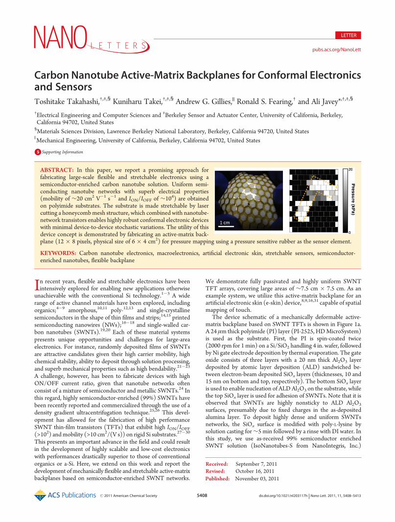
Published: November 03, 2011 r2011 American Chemical Society 5408 dx.doi.org/10.1021/nl203117h | Nano Lett. 2011, 11, 5408–5413 LETTER pubs.acs.org/NanoLett Carbon Nanotube Active-Matrix Backplanes for Conformal Electronics and Sensors Toshitake Takahashi, †,‡,§ Kuniharu Takei, †,‡,§ Andrew G. Gillies, || Ronald S. Fearing, † and Ali Javey* ,†,‡,§ † Electrical Engineering and Computer Sciences and ‡ Berkeley Sensor and Actuator Center, University of California, Berkeley, California 94702, United States § Materials Sciences Division, Lawrence Berkeley National Laboratory, Berkeley, California 94720, United States ) Mechanical Engineering, University of California, Berkeley, California 94702, United States b S Supporting Information I n recent years, flexible and stretchable electronics have been intensively explored for enabling new applications otherwise unachievable with the conventional Si technology. 13 A wide range of active channel materials have been explored, including organics; 49 amorphous, 10,11 poly- 12,13 and single-crystalline semiconductors in the shape of thin films and strips; 14,15 printed semiconducting nanowires (NWs); 1618 and single-walled car- bon nanotubes (SWNTs). 19,20 Each of these material systems presents unique opportunities and challenges for large-area electronics. For instance, randomly deposited films of SWNTs are attractive candidates given their high carrier mobility, high chemical stability, ability to deposit through solution processing, and superb mechanical properties such as high bendability. 2123 A challenge, however, has been to fabricate devices with high ON/OFF current ratio, given that nanotube networks often consist of a mixture of semiconductor and metallic SWNTs. 24 In this regard, highly semiconductor-enriched (99%) SWNTs have been recently reported and commercialized through the use of a density gradient ultracentrifugation technique. 25,26 This devel- opment has allowed for the fabrication of high performance SWNT thin-film transistors (TFTs) that exhibit high I ON /I OFF (>10 2 ) and mobility (>10 cm 2 /(V s)) on rigid Si substrates. 2730 This presents an important advance in the field and could result in the development of highly scalable and low-cost electronics with performances drastically superior to those of conventional organics or a-Si. Here, we extend on this work and report the development of mechanically flexible and stretchable active-matrix backplanes based on semiconductor-enriched SWNT networks. We demonstrate fully passivated and highly uniform SWNT TFT arrays, covering large areas of ∼7.5 cm 7.5 cm. As an example system, we utilize this active-matrix backplane for an artificial electronic skin (e-skin) device, 8,9,16,31 capable of spatial mapping of touch. The device schematic of a mechanically deformable active- matrix backplane based on SWNT TFTs is shown in Figure 1a. A 24 μm thick polyimide (PI) layer (PI-2525, HD MicroSystem) is used as the substrate. First, the PI is spin-coated twice (2000 rpm for 1 min) on a Si/SiO 2 handling 4 in. wafer, followed by Ni gate electrode deposition by thermal evaporation. The gate oxide consists of three layers with a 20 nm thick Al 2 O 3 layer deposited by atomic layer deposition (ALD) sandwiched be- tween electron-beam deposited SiO x layers (thicknesses, 10 and 15 nm on bottom and top, respectively). The bottom SiO x layer is used to enable nucleation of ALD Al 2 O 3 on the substrate, while the top SiO x layer is used for adhesion of SWNTs. Note that it is observed that SWNTs are highly nonsticky to ALD Al 2 O 3 surfaces, presumably due to fixed charges in the as-deposited alumina layer. To deposit highly dense and uniform SWNTs networks, the SiO x surface is modified with poly-L-lysine by solution casting for ∼5 min followed by a rinse with DI water. In this study, we use as-received 99% semiconductor enriched SWNT solution (IsoNanotubes-S from NanoIntegris, Inc.) Received: September 7, 2011 Revised: October 16, 2011 ABSTRACT: In this paper, we report a promising approach for fabricating large-scale flexible and stretchable electronics using a semiconductor-enriched carbon nanotube solution. Uniform semi- conducting nanotube networks with superb electrical properties (mobility of ∼20 cm 2 V 1 s 1 and I ON /I OFF of ∼10 4 ) are obtained on polyimide substrates. The substrate is made stretchable by laser cutting a honeycomb mesh structure, which combined with nanotube- network transistors enables highly robust conformal electronic devices with minimal device-to-device stochastic variations. The utility of this device concept is demonstrated by fabricating an active-matrix back- plane (12 8 pixels, physical size of 6 4 cm 2 ) for pressure mapping using a pressure sensitive rubber as the sensor element. KEYWORDS: Carbon nanotube electronics, macroelectronics, artificial electronic skin, stretchable sensors, semiconductor- enriched nanotubes, flexible backplane
Transcript of CarbonNanotubeActive ...nano.eecs.berkeley.edu/publications/NanoLett_2011_CNT_Backplane.pdf ·...
Published: November 03, 2011
r 2011 American Chemical Society 5408 dx.doi.org/10.1021/nl203117h |Nano Lett. 2011, 11, 5408–5413
LETTER
pubs.acs.org/NanoLett
Carbon Nanotube Active-Matrix Backplanes for Conformal Electronicsand SensorsToshitake Takahashi,†,‡,§ Kuniharu Takei,†,‡,§ Andrew G. Gillies,|| Ronald S. Fearing,† and Ali Javey*,†,‡,§
†Electrical Engineering and Computer Sciences and ‡Berkeley Sensor and Actuator Center, University of California, Berkeley,California 94702, United States§Materials Sciences Division, Lawrence Berkeley National Laboratory, Berkeley, California 94720, United States
)Mechanical Engineering, University of California, Berkeley, California 94702, United States
bS Supporting Information
In recent years, flexible and stretchable electronics have beenintensively explored for enabling new applications otherwise
unachievable with the conventional Si technology.1�3 A widerange of active channel materials have been explored, includingorganics;4�9 amorphous,10,11 poly-12,13 and single-crystallinesemiconductors in the shape of thin films and strips;14,15 printedsemiconducting nanowires (NWs);16�18 and single-walled car-bon nanotubes (SWNTs).19,20 Each of these material systemspresents unique opportunities and challenges for large-areaelectronics. For instance, randomly deposited films of SWNTsare attractive candidates given their high carrier mobility, highchemical stability, ability to deposit through solution processing,and superb mechanical properties such as high bendability.21�23
A challenge, however, has been to fabricate devices with highON/OFF current ratio, given that nanotube networks oftenconsist of a mixture of semiconductor and metallic SWNTs.24 Inthis regard, highly semiconductor-enriched (99%) SWNTs havebeen recently reported and commercialized through the use of adensity gradient ultracentrifugation technique.25,26 This devel-opment has allowed for the fabrication of high performanceSWNT thin-film transistors (TFTs) that exhibit high ION/IOFF(>102) andmobility (>10 cm2/(V s)) on rigid Si substrates.27�30
This presents an important advance in the field and could resultin the development of highly scalable and low-cost electronicswith performances drastically superior to those of conventionalorganics or a-Si. Here, we extend on this work and report thedevelopment of mechanically flexible and stretchable active-matrixbackplanes based on semiconductor-enriched SWNT networks.
We demonstrate fully passivated and highly uniform SWNTTFT arrays, covering large areas of ∼7.5 cm � 7.5 cm. As anexample system, we utilize this active-matrix backplane for anartificial electronic skin (e-skin) device,8,9,16,31 capable of spatialmapping of touch.
The device schematic of a mechanically deformable active-matrix backplane based on SWNT TFTs is shown in Figure 1a.A 24 μm thick polyimide (PI) layer (PI-2525, HDMicroSystem)is used as the substrate. First, the PI is spin-coated twice(2000 rpm for 1 min) on a Si/SiO2 handling 4 in. wafer, followedby Ni gate electrode deposition by thermal evaporation. The gateoxide consists of three layers with a 20 nm thick Al2O3 layerdeposited by atomic layer deposition (ALD) sandwiched be-tween electron-beam deposited SiOx layers (thicknesses, 10 and15 nm on bottom and top, respectively). The bottom SiOx layeris used to enable nucleation of ALDAl2O3 on the substrate, whilethe top SiOx layer is used for adhesion of SWNTs. Note that it isobserved that SWNTs are highly nonsticky to ALD Al2O3
surfaces, presumably due to fixed charges in the as-depositedalumina layer. To deposit highly dense and uniform SWNTsnetworks, the SiOx surface is modified with poly-L-lysine bysolution casting for∼5 min followed by a rinse with DI water. Inthis study, we use as-received 99% semiconductor enrichedSWNT solution (IsoNanotubes-S from NanoIntegris, Inc.)
Received: September 7, 2011Revised: October 16, 2011
ABSTRACT: In this paper, we report a promising approach forfabricating large-scale flexible and stretchable electronics using asemiconductor-enriched carbon nanotube solution. Uniform semi-conducting nanotube networks with superb electrical properties(mobility of ∼20 cm2 V�1 s�1 and ION/IOFF of ∼104) are obtainedon polyimide substrates. The substrate is made stretchable by lasercutting a honeycombmesh structure, which combined with nanotube-network transistors enables highly robust conformal electronic deviceswith minimal device-to-device stochastic variations. The utility of thisdevice concept is demonstrated by fabricating an active-matrix back-plane (12 � 8 pixels, physical size of 6 � 4 cm2) for pressure mapping using a pressure sensitive rubber as the sensor element.
KEYWORDS: Carbon nanotube electronics, macroelectronics, artificial electronic skin, stretchable sensors, semiconductor-enriched nanotubes, flexible backplane
5409 dx.doi.org/10.1021/nl203117h |Nano Lett. 2011, 11, 5408–5413
Nano Letters LETTER
without any densification. SWNTs were then deposited bysolution casting followed by rinse with DI water.
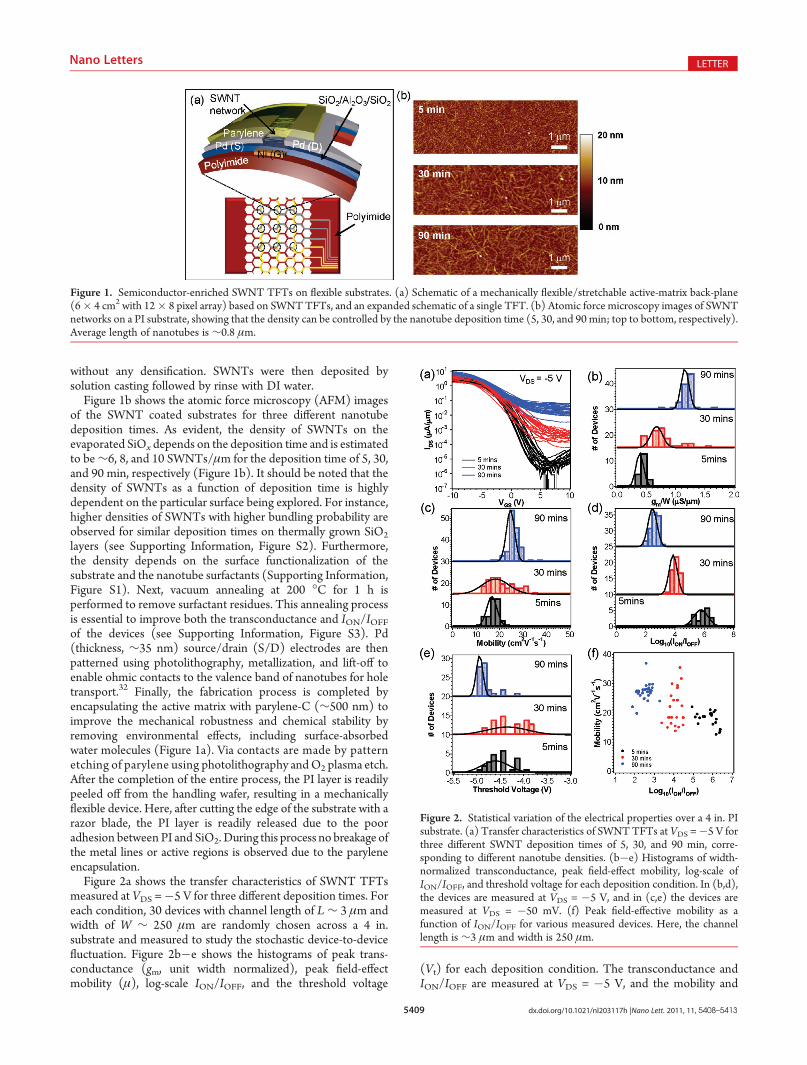
Figure 1b shows the atomic force microscopy (AFM) imagesof the SWNT coated substrates for three different nanotubedeposition times. As evident, the density of SWNTs on theevaporated SiOx depends on the deposition time and is estimatedto be∼6, 8, and 10 SWNTs/μm for the deposition time of 5, 30,and 90 min, respectively (Figure 1b). It should be noted that thedensity of SWNTs as a function of deposition time is highlydependent on the particular surface being explored. For instance,higher densities of SWNTs with higher bundling probability areobserved for similar deposition times on thermally grown SiO2
layers (see Supporting Information, Figure S2). Furthermore,the density depends on the surface functionalization of thesubstrate and the nanotube surfactants (Supporting Information,Figure S1). Next, vacuum annealing at 200 �C for 1 h isperformed to remove surfactant residues. This annealing processis essential to improve both the transconductance and ION/IOFFof the devices (see Supporting Information, Figure S3). Pd(thickness, ∼35 nm) source/drain (S/D) electrodes are thenpatterned using photolithography, metallization, and lift-off toenable ohmic contacts to the valence band of nanotubes for holetransport.32 Finally, the fabrication process is completed byencapsulating the active matrix with parylene-C (∼500 nm) toimprove the mechanical robustness and chemical stability byremoving environmental effects, including surface-absorbedwater molecules (Figure 1a). Via contacts are made by patternetching of parylene using photolithography andO2 plasma etch.After the completion of the entire process, the PI layer is readilypeeled off from the handling wafer, resulting in a mechanicallyflexible device. Here, after cutting the edge of the substrate with arazor blade, the PI layer is readily released due to the pooradhesion between PI and SiO2. During this process no breakage ofthe metal lines or active regions is observed due to the paryleneencapsulation.
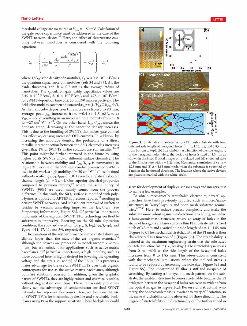
Figure 2a shows the transfer characteristics of SWNT TFTsmeasured at VDS =�5 V for three different deposition times. Foreach condition, 30 devices with channel length of L∼ 3 μm andwidth of W ∼ 250 μm are randomly chosen across a 4 in.substrate and measured to study the stochastic device-to-devicefluctuation. Figure 2b�e shows the histograms of peak trans-conductance (gm, unit width normalized), peak field-effectmobility (μ), log-scale ION/IOFF, and the threshold voltage
(Vt) for each deposition condition. The transconductance andION/IOFF are measured at VDS = �5 V, and the mobility and
Figure 1. Semiconductor-enriched SWNT TFTs on flexible substrates. (a) Schematic of a mechanically flexible/stretchable active-matrix back-plane(6� 4 cm2 with 12� 8 pixel array) based on SWNTTFTs, and an expanded schematic of a single TFT. (b) Atomic force microscopy images of SWNTnetworks on a PI substrate, showing that the density can be controlled by the nanotube deposition time (5, 30, and 90 min; top to bottom, respectively).Average length of nanotubes is ∼0.8 μm.
Figure 2. Statistical variation of the electrical properties over a 4 in. PIsubstrate. (a) Transfer characteristics of SWNTTFTs at VDS =�5 V forthree different SWNT deposition times of 5, 30, and 90 min, corre-sponding to different nanotube densities. (b�e) Histograms of width-normalized transconductance, peak field-effect mobility, log-scale ofION/IOFF, and threshold voltage for each deposition condition. In (b,d),the devices are measured at VDS = �5 V, and in (c,e) the devices aremeasured at VDS = �50 mV. (f) Peak field-effective mobility as afunction of ION/IOFF for various measured devices. Here, the channellength is ∼3 μm and width is 250 μm.
5410 dx.doi.org/10.1021/nl203117h |Nano Lett. 2011, 11, 5408–5413
Nano Letters LETTER
threshold voltage are measured at VDS =�50 mV. Calculation ofthe gate oxide capacitance must be addressed in the case of theSWNT network device.33 Here, the effect of electrostatic cou-pling between nanotubes is considered with the followingequation:
Ci ¼ 12πε
lnL0
R
sinhπ2dL0
� �
π
26664
37775 þ C�1
Q
8>>><>>>:
9>>>=>>>;
�1
L�10
where 1/Λ0 is the density of nanotubes,CQ = 4.0� 10�10 F/m isthe quantum capacitance of nanotubes (refs 34 and 35), d is theoxide thickness, and R = 0.7 nm is the average radius ofnanotubes. The calculated gate oxide capacitance values are2.45 � 108 F/cm2, 3.16 � 108 F/cm2, and 3.78 � 108 F/cm2
for SWNTdeposition time of 5, 30, and 90min, respectively. Thefield-effectmobility can then be extracted as,μ= (L/VDSCi)(gm/W).As the nanotube deposition time increases from 5 to 90 min,average peak gm increases from ∼0.4 to 1.5 μS/μm atVDS = �5 V, resulting in an increased hole mobility from ∼18to ∼27 cm2 V�1 s�1. On the other hand, ION/IOFF shows theopposite trend, decreasing as the nanotube density increases.This is due to the bundling of SWNTs that makes gate controlless effective, causing increased OFF-currents. In addition, byincreasing the nanotube density, the probability of a directmetallic interconnection between the S/D electrodes increasesgiven that 1% of SWNTs in the solution are still metallic.29,30
This point might be further improved in the future by usinghigher purity SWNTs and/or different surface chemistry. Therelationship between mobility and ION/IOFF is summarized inFigure 2f. Because of the 99% semiconductor-enriched SWNTsused in this work, a highmobility of∼20 cm2 V�1 s�1 is obtainedwithout sacrificing ION/IOFF (∼104) even for a relatively shorterchannel length (L ∼ 3 μm). Our superior electrical propertiescompared to previous reports,30 where the same purity ofSWNTs (99%) are used, mainly comes from the processdifference. In this work, the SiO2 surface is modified with poly-L-lysine, as opposed to APTES in previous reports,30 resulting indenser SWNT networks. And subsequent removal of surfactantresidue by vacuum annealing improves the ION/IOFF (seeSupporting Information, Figure S3). Of particular importance,uniformity of the explored SWNT TFT technology on flexiblesubstrates is impressive. Focusing on the 90 min depositioncondition, the standard deviation for gm, μ, log(ION/IOFF), andVt are ∼11, 17, 11, and 3%, respectively.
The variations of the key performance metrics listed above areslightly larger than the state-of-the art organic materials36
although the devices are processed in noncleanroom environ-ment, but are sufficient for applications such as active-matrixbackplanes. Of particular importance, a high mobility, such asthose obtained here, is highly desired for lowering the operatingvoltage and the size (i.e., width) of the FETs. This presents amajor advantage for the use of SWNT TFTs over their organiccounterparts for use as the active matrix backplanes, althoughboth are solution-processed. In addition, given the graphiticnature of SWNTs, they are highly robust and chemically stable,without degradation over time. These remarkable propertiesclearly set the advantage of semiconductor-enriched SWNTnetworks for large-area electronics. Here, we focus on the useof SWNT TFTs for mechanically flexible and stretchable back-planes using PI as the support substrate. These backplanes could
serve for development of displays, sensor arrays and imagers, justto name a few examples.
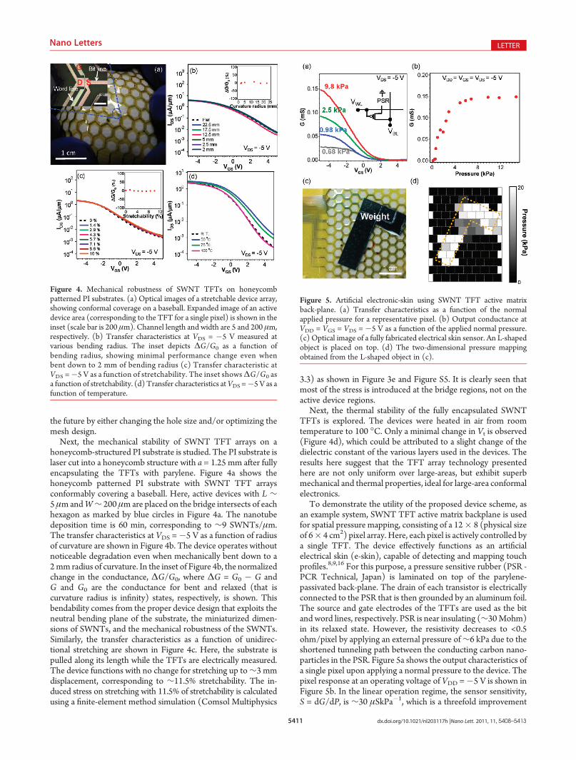
To obtain mechanically stretchable electronics, several ap-proaches have been previously reported such as micro/nano-structures in “wavy” layouts and open mesh substrate geome-tries.9,37,38 Here, to reduce process complexity and make thesubstrate more robust against unidirectional stretching, we utilizea honeycomb mesh structure, where an array of holes in theshape of hexagons are laser cut on a thin PI substrate with a fixedpitch of 3.3 mm and a varied hole side-length of a = 1�1.85 mm(Figure 3a). The mechanical stretchability of the PI mesh is thencharacterized as a function of a (Figure 3b). The stretchability isdefined as the maximum engineering strain that the substratescan tolerate before failure (i.e., breakage). The stretchability increasesfrom 0 to ∼60% as the side length of the hexagonal holesincreases from 0 to 1.85 mm. This observation is consistentwith the mechanical simulations, where the induced stress isfound to be reduced by increasing the hole size (Figure 3e,f andFigure S5). The unpatterned PI film is stiff and incapable ofstretching. By cutting a honeycomb mesh pattern on the sub-strate, the enabled structure becomes stretchable because the PIbridges in-between the hexagonal holes can twist as evident fromthe optical images in Figure 3c,d. Because of a structural sym-metry, the honeycomb mesh is invariant to every 60� rotation, sothe same stretchability can be observed for those directions. Thedegree of stretchability and directionality can be further tuned in
Figure 3. Stretchable PI substrates. (a) PI mesh substrate with fourdifferent side length of hexagonal holes (a = 1, 1.25, 1.5, and 1.85 mm,from bottom to top). (b) Stretchability as a function of the side length, a,of the hexagonal holes. Here, the period of holes is fixed at 3.3 mm asshown in the inset. Optical images of (c) relaxed and (d) stretched stateof the PI substrate with a = 1.25 mm. Mechanical simulation of (e) a =1.25 mm and (f) a = 1.85 mm mesh, when the substrate is stretched by2 mm in the horizontal direction. The location where the active devicesare placed is marked with the white circle.
5411 dx.doi.org/10.1021/nl203117h |Nano Lett. 2011, 11, 5408–5413
Nano Letters LETTER
the future by either changing the hole size and/or optimizing themesh design.
Next, the mechanical stability of SWNT TFT arrays on ahoneycomb-structured PI substrate is studied. The PI substrate islaser cut into a honeycomb structure with a = 1.25 mm after fullyencapsulating the TFTs with parylene. Figure 4a shows thehoneycomb patterned PI substrate with SWNT TFT arraysconformably covering a baseball. Here, active devices with L ∼5 μmandW∼ 200 μm are placed on the bridge intersects of eachhexagon as marked by blue circles in Figure 4a. The nanotubedeposition time is 60 min, corresponding to ∼9 SWNTs/μm.The transfer characteristics at VDS =�5 V as a function of radiusof curvature are shown in Figure 4b. The device operates withoutnoticeable degradation even when mechanically bent down to a2mm radius of curvature. In the inset of Figure 4b, the normalizedchange in the conductance, ΔG/G0, where ΔG = G0 � G andG and G0 are the conductance for bent and relaxed (that iscurvature radius is infinity) states, respectively, is shown. Thisbendability comes from the proper device design that exploits theneutral bending plane of the substrate, the miniaturized dimen-sions of SWNTs, and the mechanical robustness of the SWNTs.Similarly, the transfer characteristics as a function of unidirec-tional stretching are shown in Figure 4c. Here, the substrate ispulled along its length while the TFTs are electrically measured.The device functions with no change for stretching up to∼3 mmdisplacement, corresponding to ∼11.5% stretchability. The in-duced stress on stretching with 11.5% of stretchability is calculatedusing a finite-element method simulation (Comsol Multiphysics
3.3) as shown in Figure 3e and Figure S5. It is clearly seen thatmost of the stress is introduced at the bridge regions, not on theactive device regions.
Next, the thermal stability of the fully encapsulated SWNTTFTs is explored. The devices were heated in air from roomtemperature to 100 �C. Only a minimal change in Vt is observed(Figure 4d), which could be attributed to a slight change of thedielectric constant of the various layers used in the devices. Theresults here suggest that the TFT array technology presentedhere are not only uniform over large-areas, but exhibit superbmechanical and thermal properties, ideal for large-area conformalelectronics.
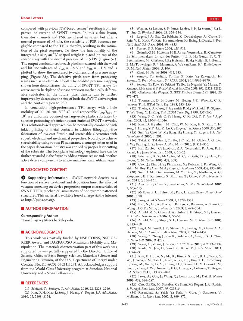
To demonstrate the utility of the proposed device scheme, asan example system, SWNT TFT active matrix backplane is usedfor spatial pressure mapping, consisting of a 12� 8 (physical sizeof 6� 4 cm2) pixel array. Here, each pixel is actively controlled bya single TFT. The device effectively functions as an artificialelectrical skin (e-skin), capable of detecting and mapping touchprofiles.8,9,16 For this purpose, a pressure sensitive rubber (PSR -PCR Technical, Japan) is laminated on top of the parylene-passivated back-plane. The drain of each transistor is electricallyconnected to the PSR that is then grounded by an aluminum foil.The source and gate electrodes of the TFTs are used as the bitand word lines, respectively. PSR is near insulating (∼30Mohm)in its relaxed state. However, the resistivity decreases to <0.5ohm/pixel by applying an external pressure of∼6 kPa due to theshortened tunneling path between the conducting carbon nano-particles in the PSR. Figure 5a shows the output characteristics ofa single pixel upon applying a normal pressure to the device. Thepixel response at an operating voltage of VDD =�5 V is shown inFigure 5b. In the linear operation regime, the sensor sensitivity,S = dG/dP, is ∼30 μSkPa�1, which is a threefold improvement
Figure 4. Mechanical robustness of SWNT TFTs on honeycombpatterned PI substrates. (a) Optical images of a stretchable device array,showing conformal coverage on a baseball. Expanded image of an activedevice area (corresponding to the TFT for a single pixel) is shown in theinset (scale bar is 200 μm). Channel length and width are 5 and 200 μm,respectively. (b) Transfer characteristics at VDS = �5 V measured atvarious bending radius. The inset depicts ΔG/G0 as a function ofbending radius, showing minimal performance change even whenbent down to 2 mm of bending radius (c) Transfer characteristic atVDS =�5 V as a function of stretchability. The inset showsΔG/G0 asa function of stretchability. (d) Transfer characteristics atVDS =�5 V as afunction of temperature.
Figure 5. Artificial electronic-skin using SWNT TFT active matrixback-plane. (a) Transfer characteristics as a function of the normalapplied pressure for a representative pixel. (b) Output conductance atVDD = VGS = VDS = �5 V as a function of the applied normal pressure.(c) Optical image of a fully fabricated electrical skin sensor. An L-shapedobject is placed on top. (d) The two-dimensional pressure mappingobtained from the L-shaped object in (c).
5412 dx.doi.org/10.1021/nl203117h |Nano Lett. 2011, 11, 5408–5413
Nano Letters LETTER
compared with previous NW-based sensor4 resulting from im-proved on-current of SWNT devices. In this e-skin layout,transistor channels and PSR are placed in series, but after anormal pressure of >6 kPa, the resistivity of PSR becomes ne-gligible compared to the TFTs, thereby, resulting in the satura-tion of the pixel response. To show the functionality of theintegrated e-skin, an “L”-shaped weight is placed on top of thesensor array with the normal pressure of ∼15 kPa (Figure 5c).The output conductance for each pixel is measured with the wordand bit line voltages of VWL = �5 V and VBL = �1 V and isplotted to show the measured two-dimensional pressure map-ping (Figure 5d). The defective pixels stem from processingissues such as inadequate lift-off. The enabled pressure mappingshown here demonstrates the utility of SWNT TFT arrays foractive-matrix backplane of sensor arrays onmechanically deform-able substrates. In the future, pixel density can be furtherimproved by decreasing the size of both the SWNT active regionand the contact region to PSR.
In conclusion, high-performance TFT arrays with a holemobility of 20�30 cm2 V�1 s�1 and respectable ION/IOFF ∼104 are uniformly obtained on large-scale plastic substrates bysolution processing of semiconductor-enriched SWNT networks.This solution-based approach can be potentially combined withinkjet printing of metal contacts to achieve lithography-freefabrication of low-cost flexible and stretchable electronics withsuperb electrical and mechanical properties. Notably, to achievestretchability using robust PI substrates, a concept often used inthe paper decoration industry was applied by proper laser cuttingof the substrate. The back-plane technology explored here can befurther expanded in the future by adding various sensor and/or otheractive device components to enable multifunctional artificial skins.
’ASSOCIATED CONTENT
bS Supporting Information. SWNT-network density as afunction of surface treatment and deposition time; the effect ofvacuum annealing on device properties; output characteristics ofSWNT TFTs; mechanical simulations of honeycomb patternedstructures. This material is available free of charge via the Internetat http://pubs.acs.org.
’AUTHOR INFORMATION
Corresponding Author*E-mail: [email protected].
’ACKNOWLEDGMENT
This work was partially funded by NSF COINS, NSF CA-REER Award, and DARPA/DSO Maximum Mobility and Ma-nipulation. The materials characterization part of this work wassupported by was partially supported by the Director, Office ofScience, Office of Basic Energy Sciences, Materials Sciences andEngineering Division, of the U.S. Department of Energy underContract No. DE-AC02-05CH11231. A.J. acknowledges supportfrom the World Class University program at Sunchon NationalUniversity and a Sloan Fellowship.
’REFERENCES
(1) Sekitani, T.; Someya, T. Adv. Mater. 2010, 22, 2228–2246.(2) Kim, D. H.; Xiao, J.; Song, J.; Huang, Y.; Rogers, J. A. Adv. Mater.
2010, 22, 2108–2124.
(3) Wagner, S.; Lacour, S. P.; Jones, J.; Hsu, P. H. I.; Sturm, J. C.; Li,T.; Suo, Z. Physica E 2004, 25, 326–334.
(4) Rogers, J. A.; Bao, Z.; Baldwin, K.; Dodabalapur, A.; Crone, B.;Raju, V. R.; Kuck, V.; Katz, H.; Amundson, K.; Ewing, J.; Drzaic, P. Proc.Natl. Acad. Sci. U.S.A. 2001, 98, 4835.
(5) Forrest, S. F. Nature 2004, 428, 911.(6) Gelinck, G. H.; Huitema, H. E. A.; van Veenendaal, E.; Cantatore,
E.; Schrijnemakers, L.; van der Putten, J. B. P. H.; Genus, T. C. T.;Beenhakkers, M.; Giesbers, J. B.; Huisman, B. H.; Meijer, E. J.; Benito,E. M.; Touwslager, F. J.; Marsman, A. W.; van Rens, B. J. E.; de Leeuw,D. M. Nat. Mater. 2004, 3, 106.
(7) Klauk, H. Nature 2008, 451, 533.(8) Someya, T.; Sekitani, T.; Iba, S.; Kato, Y.; Kawaguchi, H.;
Sakurai, T. Proc. Natl. Acad. Sci. U.S.A. 2004, 101, 9966–9970.(9) Someya, T.; Kato, Y.; Sekitani, T.; Iba, S.; Noguchi, Y.; Murase, Y.;
Kawaguchi,H.; Sakurai,T.Proc.Natl. Acad. Sci.U.S.A.2005,102, 12321–12325.(10) Gleskova, H.; Wagner, S. IEEE Electron Device Lett. 1999, 20,
473–475.(11) Thomasson, D. B.; Bonse, M.; Huang, J. R.; Wronski, C. R.;
Jackson, T. N. IEDM Tech. Dig. 1998, 253–256.(12) Theiss, S. D.; Carey, P. G.; Smith, P.M.;Wickboldt, P.; Sigmon,
T. W.; Tung, Y. J.; King, T.-J. IEDM Tech. Dig. 1998, 257–260.(13) Wang, S. C.; Yeh, C. F.; Huang, C. K.; Dai, Y. T. Jpn. J. Appl.
Phys. 2003, 42, L1044–L1046.(14) Kim., D. H.; Ahn, J. H.; Choi, W. M.; Kim, H. S.; Kim, T. H.;
Song, J.; Huang, Y. Y.; Liu, Z.; Lu, C.; Rogers, J. A. Science 2008, 320, 507.(15) Sun, Y.; Choi, W. M.; Jiang, H.; Huang, Y.; Rogers, J. A. Nat.
Nanotechnol. 2006, 1, 201.(16) Takei, K.; Takahashi, T.; Ho, J. C.; Ko, H.; Gillies, A. G.; Leu,
P. W.; Fearing, R. S.; Javey, A. Nat. Mater. 2010, 9, 821–826.(17) Fan, Z.; Ho, J. C.; Jacobson, Z. A.; Yerushalmi, R.; Alley, R. L.;
Razavi, H.; Javey Nano Lett. 2008, 8, 20–25.(18) Friedman, R. S.; McAlpine, M. C.; Ricketts, D. S.; Ham, D.;
Lieber, C. M. Nature 2005, 434, 1085.(19) Cao, Q.; Kim, H. S.; Pimparkar, N.; Kulkarni, J. P.; Wang, C.;
Shim,M.; Roy, K.; Alam,M. A.; Rogers, J. A.Nature 2008, 454, 495–500.(20) Sun, D. M.; Timmermans, M. Y.; Tian, Y.; Nasibulin, A. G.;
Kauppinen, E. I.; Kishimoto, S.; Mizutani, T.; Ohno, Y. Nat. Nanotech-nol. 2011, 6, 156–161.
(21) Avouris, P.; Chen, Z.; Perebeinos, V. Nat Nanotechnol. 2007,2, 605–615.
(22) McEuen, P. L.; Fuhrer, M.; Park, H. IEEE Trans. Nanotechnol.2002, 1, 78.
(23) Javey, A. ACS Nano 2008, 2, 1329–1335.(24) Patil, N.; Lin, A.; Myers, E. R.; Ryu, K.; Badmaev, A.; Zhou, C.;
Wong, H.-S. P.; Mitra, S. Nano Lett. 2009, 8, 498–504.(25) Arnold, M. S.; Green, A. A.; Hulvat, J. F.; Stupp, S. I.; Hersam,
M. C. Nat. Nanotechnol. 2006, 1, 60–65.(26) Arnold, M. S.; Stupp, S. I.; Hersam, M. C. Nano Lett. 2005,
5, 713–718.(27) Engel, M.; Small, J. P.; Steiner, M.; Freitag, M.; Green, A. A.;
Hersam, M. C.; Avouris, P. ACS Nano 2008, 2, 2445–2452.(28) Wang, C.; Zhang, J.; Ryu, K.; Badmaev, A.; Arco, L. G. D.; Zhou,
C. Nano Lett. 2009, 9, 4285.(29) Wang, C.; Zhang, J.; Zhou, C. ACS Nano 2010, 4, 7123–7132.(30) Rouhi, N.; Jain, D.; Zand, K.; Burke, P. J. Adv. Mater. 2011,
23, 94–99.(31) Kim, D. H.; Lu, N.; Ma, R.; Kim, Y. S.; Kim, R. H.; Wang, S.;
Wu, J.; Won, S. M.; Tao, H.; Islam, A.; Yu, K. J.; Kim, T. I.; Chowdhury,R.; Ying, M.; Xu, L.; Li, M.; Chung, H. J.; Keum, H.; McCormick, M.;Liu, P.; Zhang, Y. W.; Omenetto, F. G.; Huang, Y.; Coleman, T.; Rogers,J. A. Science 2011, 333, 838–843.
(32) Javey, A.; Guo, J.; Wang, Q.; Lundstrom, M.; Dai, H. Nature2003, 424, 654–657.
(33) Cao, Q.; Xia, M.; Kocabas, C.; Shim, M.; Rogers, J. A.; Rotkin,S. V. Appl. Phys. Lett. 2007, 90, 023516.
(34) Rosenblatt, S.; Yaish, Y.; Park, J.; Gore, J.; Sazonova, V.;McEuen, P. L. Nano Lett. 2002, 2, 869–872.

5413 dx.doi.org/10.1021/nl203117h |Nano Lett. 2011, 11, 5408–5413
Nano Letters LETTER
(35) Javey, A.; Kim, H.; Brink, M.; Wang, Q.; Ural, A.; Guo, J.;McIntyre, P.; McEuen, P.; Lundstrom, M.; Dai, H. Nat. Mater. 2002,1, 241–246.(36) Klauk, H. Organic Electronics: Materials, Manufacturing and
Applications; Wiley-VCH: New York, 2006.(37) Kim, D. H.; Rogers, J. A. Adv. Mater. 2008, 20, 4887–4892.(38) Rogers, J. A.; Someya, T.; Huang, Y. Science 2010, 327, 1603–1607.

S1
Supporting Information
Carbon Nanotube Active Matrix Backplanes for Conformal Electronics
Toshitake Takahashi1,2,3, Kuniharu Takei1,2,3, Andrew G. Gillies4, Ronald S. Fearing1 and
Ali Javey1,2,3
1 Electrical Engineering and Computer Sciences, University of California, Berkeley, CA 94702
2 Berkeley Sensor and Actuator Center, University of California, Berkeley, CA 94720
3 Materials Sciences Division, Lawrence Berkeley National Laboratory, Berkeley, CA 94720
4 Mechanical Engineering, University of California, Berkeley, CA 94702
S2
(c) (d)
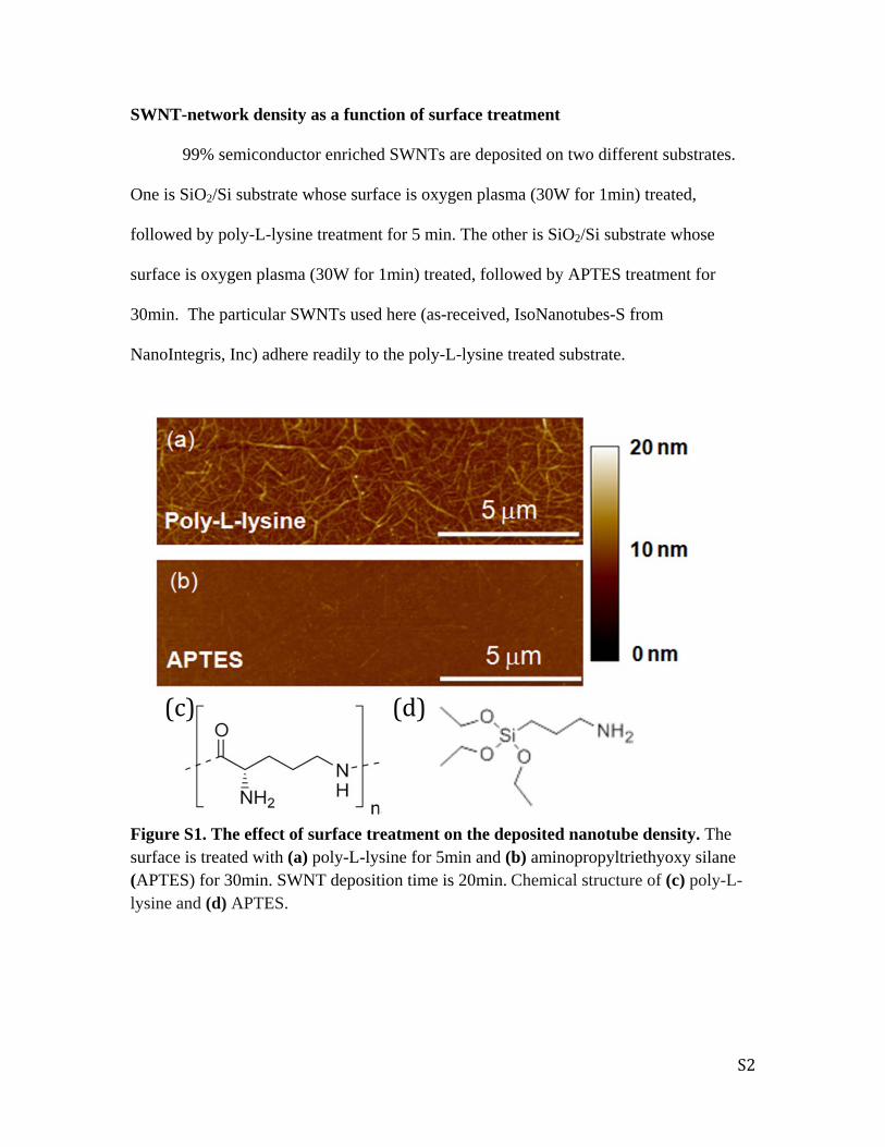
SWNT-network density as a function of surface treatment 99% semiconductor enriched SWNTs are deposited on two different substrates.
One is SiO2/Si substrate whose surface is oxygen plasma (30W for 1min) treated,
followed by poly-L-lysine treatment for 5 min. The other is SiO2/Si substrate whose
surface is oxygen plasma (30W for 1min) treated, followed by APTES treatment for
30min. The particular SWNTs used here (as-received, IsoNanotubes-S from
NanoIntegris, Inc) adhere readily to the poly-L-lysine treated substrate.
Figure S1. The effect of surface treatment on the deposited nanotube density. The surface is treated with (a) poly-L-lysine for 5min and (b) aminopropyltriethyoxy silane (APTES) for 30min. SWNT deposition time is 20min. Chemical structure of (c) poly-L-lysine and (d) APTES.
S3
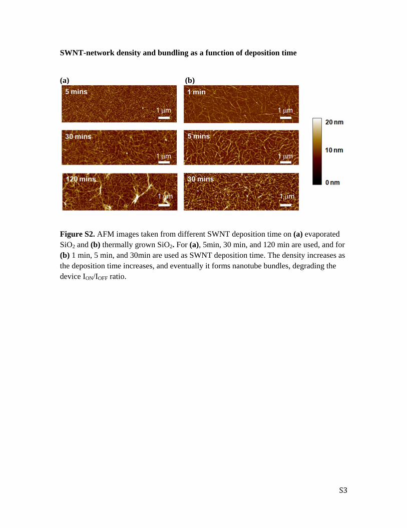
SWNT-network density and bundling as a function of deposition time (a) (b)
Figure S2. AFM images taken from different SWNT deposition time on (a) evaporated SiO2 and (b) thermally grown SiO2. For (a), 5min, 30 min, and 120 min are used, and for (b) 1 min, 5 min, and 30min are used as SWNT deposition time. The density increases as the deposition time increases, and eventually it forms nanotube bundles, degrading the device ION/IOFF ratio.
S4
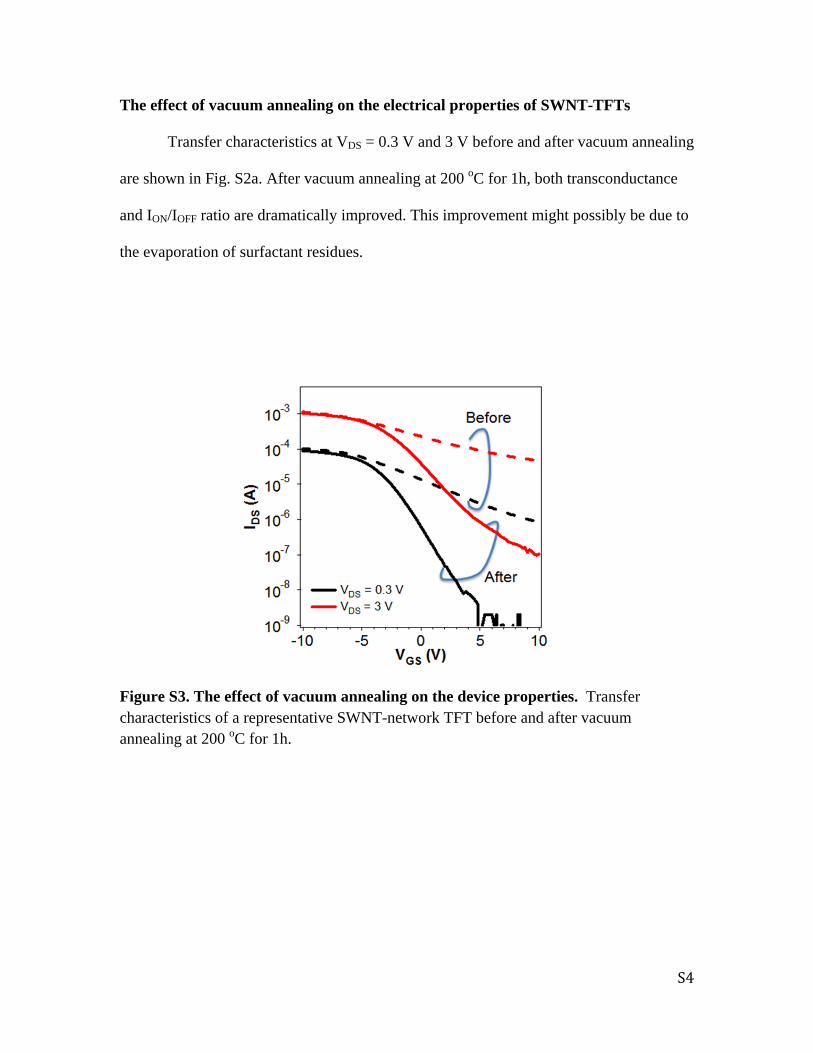
The effect of vacuum annealing on the electrical properties of SWNT-TFTs Transfer characteristics at VDS = 0.3 V and 3 V before and after vacuum annealing
are shown in Fig. S2a. After vacuum annealing at 200 oC for 1h, both transconductance
and ION/IOFF ratio are dramatically improved. This improvement might possibly be due to
the evaporation of surfactant residues.
Figure S3. The effect of vacuum annealing on the device properties. Transfer characteristics of a representative SWNT-network TFT before and after vacuum annealing at 200 oC for 1h.
S5
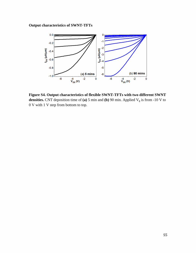
Output characteristics of SWNT-TFTs
Figure S4. Output characteristics of flexible SWNT-TFTs with two different SWNT densities. CNT deposition time of (a) 5 min and (b) 90 min. Applied Vg is from -10 V to 0 V with 1 V step from bottom to top.
S6
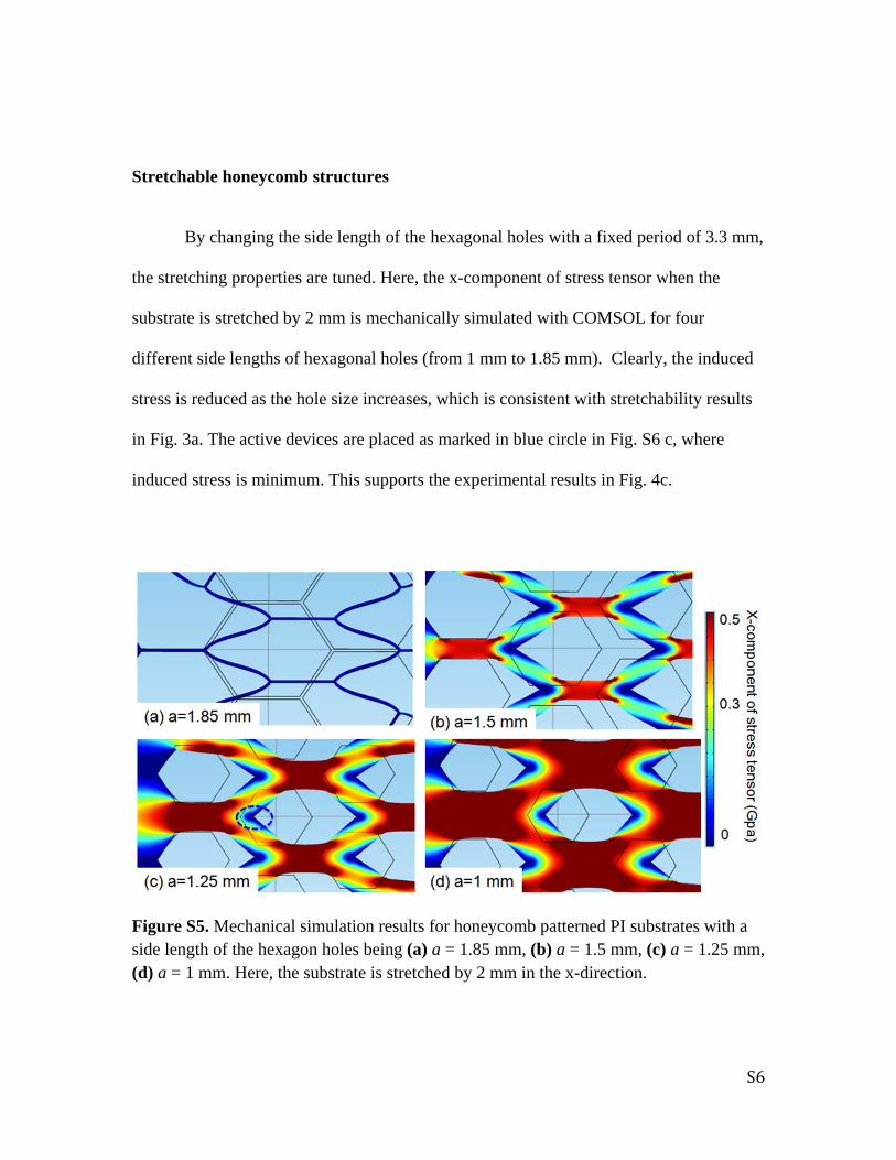
Stretchable honeycomb structures
By changing the side length of the hexagonal holes with a fixed period of 3.3 mm,
the stretching properties are tuned. Here, the x-component of stress tensor when the
substrate is stretched by 2 mm is mechanically simulated with COMSOL for four
different side lengths of hexagonal holes (from 1 mm to 1.85 mm). Clearly, the induced
stress is reduced as the hole size increases, which is consistent with stretchability results
in Fig. 3a. The active devices are placed as marked in blue circle in Fig. S6 c, where
induced stress is minimum. This supports the experimental results in Fig. 4c.
Figure S5. Mechanical simulation results for honeycomb patterned PI substrates with a side length of the hexagon holes being (a) a = 1.85 mm, (b) a = 1.5 mm, (c) a = 1.25 mm, (d) a = 1 mm. Here, the substrate is stretched by 2 mm in the x-direction.