CARBON NANOTUBE TRANSISTORS, SENSORS, AND BEYOND · CARBON NANOTUBE TRANSISTORS, SENSORS, AND...
191
CARBON NANOTUBE TRANSISTORS, SENSORS, AND BEYOND A Dissertation Presented to the Faculty of the Graduate School of Cornell University In Partial Fulfillment of the Requirements for the Degree of Doctor of Philosophy by Xinjian Zhou January 2008
Transcript of CARBON NANOTUBE TRANSISTORS, SENSORS, AND BEYOND · CARBON NANOTUBE TRANSISTORS, SENSORS, AND...

CARBON NANOTUBE TRANSISTORS, SENSORS, AND BEYOND
A Dissertation
Presented to the Faculty of the Graduate School
of Cornell University
In Partial Fulfillment of the Requirements for the Degree of
Doctor of Philosophy
by
Xinjian Zhou
January 2008


CARBON NANOTUBE TRANSISTORS, SENSORS, AND BEYOND
Xinjian Zhou, Ph. D.
Cornell University 2008
Carbon nanotubes are tiny hollow cylinders, made from a single graphene
sheet, that possess many amazing properties. Another reason why nanotubes have
generated intense research activities from scientists of various disciplines is they
represent a new class of materials for the study of one-dimensional physics. In this
thesis we investigate the electrical transport of semiconducting single-walled carbon
nanotubes and their potential applications as biological sensors.
Electrons have been predicted, by theoretical physicists, to go through
nanotubes without much resistance. But this has not been properly quantified
experimentally, and the origin of the routinely observed large resistance in nanotubes
is not clear. In this thesis we show that in moderate long high quality nanotubes the
electrical transport is limited by electron-phonon scattering. Systematic studies are
carried out using many devices of different diameters at various temperatures. The
resistance and inverse of peak mobility are observed to decrease linearly with
temperature, indicating the influence of phonons. The conductance and peak mobility
scales with nanotube diameters also, in a linear fashion and quadratic fashion
respectively. Based on electron-phonon scattering, a theory model is developed that
can not only predict how the resistance changes with gate voltage but also explain the
observed temperature and diameter dependence. This work clarifies the nature of
electrical transport in nanotubes and sets a performance limit of nanotube devices in
diffusive regime.

The electrical transport in nanotubes is extremely sensitive to local
electrostatic environment due to their small size, large surface to volume ratio and
high mobility, making nanotubes ideal key elements in biological sensors. In the
second part of this thesis, we integrate nanotubes with supported lipid bilayers, mimic
structures of cell membranes, and use this platform as a way to introduce biomolecules
into the vicinity of nanotubes for sensing purpose. The quality of supported lipid
bilayers near nanotubes is confirmed by probing the diffusion of lipid molecules.
Nanotubes do not slow down lipid diffusions, but act as barriers for proteins bound to
membrane embedded receptors. The ability of nanotubes to control membrane protein
diffusions can be used to study the complex correlation between protein functions and
their diffusion properties. Future efforts can be put into modulating the magnitude of
nanotube barriers with electrical potentials for deterministic controls. We also
demonstrate that the formation of lipid bilayers and the protein bindings on the
membranes can be detected by nanotubes as their conductance are changed by those
events. The sensitivity of this system can be improved to near single molecule level.

iii
BIOGRAPHICAL SKETCH
Xinjian Zhou was born 1978 in Baoding, China. He was selected to the Chinese
National Experimental Science Class in 1994 to receive intensive science education in
the Affiliated High School of Peking University in Beijing. In 1997, he attended
Peking University working toward a B.S. degree in physics. An undergraduate
research scholar program, the Chun-Tsung scholarship, led Xinjian into the wonderful
experimental research world for the first time. His diverse work ranged from
developing automated laser mode measurement system to improving metal-
semiconductor contacts. A summer research experience in 2000 in the group of Prof.
S.T. Lee at City University of Hong Kong exposed him to a world class lab and
frontier research. He continued his pursuit in physics in the United States since 2001
when he began his graduate school in the Physics Department of Cornell University.
In the summer of 2002, he joined the group of Paul McEuen and has been working in
nanoscience and nanotechnology ever since. After his defense in August 2007, he will
continue his research as a postdoc scientist at Sandia National Laboratories in
Livermore, CA.

iv
ACKNOWLEDGEMENTS
It has been a long journey to finish my graduate school. I could have never
been able to be where I am and who I am without the help of so many people.
First of all, our beloved thesis advisor, Paul McEuen, taught me so much in
science and every aspect of life. My knowledge and understanding in physics was
superficial when I joined your group. You showed us how to be observant and grasp
the essence of any phenomenon with a simple yet clear physics picture. I am also
grateful that you put extra efforts into developing our communication skills, ranging
from presentations to writings. Imagine how horrible this thesis would have been
without your comments and revisions. You shaped my personality as well. I learned
how to deal with conflicts and difficulties in life. I can put my mind into a tranquil
state, and I believe that was achieved under your subtle influence. I am so lucky to
have spent my graduate student life under the guidance of an intelligent, open-minded,
forgiving and loving advisor.
Thanks for all the help and company I received in the McEuen group. I want to
thank our older group members for teaching me all the experimental techniques and
making the lab running efficiently: Sami for showing me cleanroom processings step
by step, Ji-Yong for teaching me low temperature measurements and advanced usage
of AFM, Jun for your helpful discussions in physics, Ken for your broad knowledge in
optics and chemistry, Ethan for telling me several nanotube growth tricks, Yuval and
Alex for the setup of so many equipments for the lab, Markus for babysitting us over
the years, Vera for your new MeaSureit program. Jiwoong, Shahal and Zhaohui, my
discussions with you clarified my future direction. I am so glad to have consulted your
expert opinions. The younger generations: Patrycja, Yaqiong, Scott, Luke, Lisa, Arend,
Nathan, Sam and Jonathan, I enjoyed every minute working with you. Your diverse

v
and wonderful personalities made me home; and your extraordinary research gave me
continuous inspirations.
Most of the projects I performed were collaborative in nature. I want to thank
Prof. Carl Batt and Sonny Mark for leading me into the biology world. The DNA
project with you generated the best research pictures of my graduate school. The lipid
project cannot even get started without the inputs from Prof. Harold Craighead and
Jose Moran-Mirabal. I felt shameless to ask for new samples every week. Your
experience and knowledge in this field were indispensable to the success of this work.
I also want to thank Prof. Manfred Lindau for lending me some equipments. Jie Yao,
you are an underground hero. Your discussions and lectures made me close to biology.
Many thanks to the CNF stuff. Thank you for teaching me the processings and
keeping the facility a wonderful place. I am grateful to NBTC, who provided funding
for all my research. The CNF and NBTC symposiums were always exciting.
I received a lot of helps from people outside Cornell University, and I am
grateful to many people in the nanotube and nanobio community. Particularly I thank
Prof. Jiu Liu and Shaoming Huang for the generous disclosure of your growth
technique. Prof. Ji Ung Lee, it was a pleasure getting to know you and I enjoyed our
work together in GE for the summer of 2006.
I own big favors to many people who had written all kinds of reference letters
for me. Thank you for your kind words. Prof. McEuen, Craighead and Lee, your
letters got me my postdoc position. Prof. Marc Bockrath and Pat Collier, thank you
for supporting me in a fellowship application. Prof. Charles Lieber, Bob Austin and Yi
Cui wrote letters for another important application of mine, I cannot express my
thanks enough.
My life in Ithaca was made fun by many Chinese friends. I want to thank
Xiaodong, Hui, Chong, Ling, Yi, Jie, Feinan, Shi, Tian, Xing and Guoqiang for being

vi
the best roommates and long time friends. I want to thank the Chinese community in
the Clark Hall basement: Lucy, Miao, Jing, Zhipan, Sufei and Yongtao, for the nice
interactions between us. The people in the group of Prof. Burhman, Andrew, Nate,
Phil, Ozhan, Pat, Gregg and John, have magical ways to always cheer up my wife and
me.
Last, I want to thank my family. Although my parents are oceans apart from
me, I know you love me and pray for me everyday. The distance in between only
strengthens our connections. I am grateful to my elder brother, Xinhui, and sister-in-
law, Zhihui. Thank you for taking good care of our parents. Without you, I may not
have chosen to go this far. And Juting, thank you for spending the past seven years
together with me, sharing the bitterness and happiness of life. Your smile is always in
my mind; and making you happy is my sole motivation to achieve anything.

vii
TABLE OF CONTENTS
Biographical sketch i i i
Acknowledgements iv
List of figures ix
List of tables xii
1 Introcution to carbon nanotubes 1
1.1 Structure of nanotubes and characterization methods ........................................ 1 1.2 Impressive properties of nanotubes and potential applications.......................... 7 1.3 Problems........................................................................................................... 12 1.4 Scope of this thesis ........................................................................................... 13
2 Electronic band structure of carbon nanotubes 14
2.1 Atoms, molecules and crystals ......................................................................... 14 2.2 Tight-binding calculations of graphene band structure .................................... 15 2.3 Making nanotubes from graphene.................................................................... 25 2.4 Band structure of carbon nanotubes ................................................................. 27 2.5 Simplified band structure ................................................................................. 32 2.6 Effects of tube curvature and non-zero overlap integral .................................. 36
3 Electron-phonon scattering in semiconducting nanotubes 40
3.1 Experimental data............................................................................................. 41 3.2 Semiclassical transport, Boltzmann equation and the relaxation time approximation........................................................................................................... 48 3.3 Electron-Phonon scattering in nanotubes ......................................................... 51 3.4 A model of electron-phonon scattering limited conduction in nanotubes........ 54 3.5 Comparing data with theory ............................................................................. 58
4 Introduction to cell membranes 60
4.1 Lipids and membrane proteins form cell membranes ...................................... 61 4.2 Artificial lipid bilayers ..................................................................................... 74
5 Supported lipid bilayer/carbon nanotube hybrid 84
5.1 Prelude.............................................................................................................. 85 5.2 Forming SLBs on nanotube chips .................................................................... 90 5.3 Probing SLBs near nanotubes .......................................................................... 99 5.4 Nanotubes as barriers to protein diffusion...................................................... 102 5.5 Electrical detection of protein binding ........................................................... 108

viii
6 Conclusions 113 6.1 Summary ........................................................................................................ 113 6.2 Future directions............................................................................................. 114
A Nanotube growth 123
B Validation of the theory model in Chapter 3 131
C Funtionalization of nanotubes with DNA 139
D Electrode kinetics in solution 149
E Dimensionality of nanotubes and our universe 157
References 160

ix
LIST OF FIGURES
1.1 Models of carbon allotropies. .............................................................................2 1.2 Images of nanotubes. ..........................................................................................2 1.3 Atomically resolved image of SWNTs..............................................................5 1.4 Three examples of cover figures of major scientific journals featuring
nanotubes. ...........................................................................................................8 1.5 Nanotubes as AFM scanning tips. ....................................................................11 2.1 Electron atomic and molecular orbitals ............................................................17 2.2 Lattice of graphene. ..........................................................................................18 2.3 Plots of the graphene band structure ................................................................22 2.4 The first Brillouin zone of graphene ................................................................24 2.5 Reorganization of the first Brillouin zone ........................................................25 2.6 Making nanotubes from graphene ....................................................................26 2.7 The electron wave vector along the circumference of a nanotube is quantized28 2.8 Extracting band structure of nanotubes from that of graphene. .......................29 2.9 The subbands of a (5,5) armchair tube .............................................................30 2.10 The subbands of two zigzag tubes....................................................................32 2.11 Extracting eletron energy from its wavevector around K point. ......................34 2.12 Comparison of nanotube band structures calculated from the simplified
dispersion relation and from the more rigorous one.........................................35 2.13 Calculated bandgaps of nanotubes with different diameter and chirality when
the curvature effect is taken in account. ...........................................................36 2.14 The influence of the overlap integral a on the graphene band structure..........38 2.15 The influence of the overlap integral a on nanotube band structures. .............39 3.1 AFM image and schematic of nanotube devices..............................................41 3.2 The conductance of a device at different temperatures ....................................43 3.3 The conductance and mobility as functions of gate voltage for two different
devices ..............................................................................................................44 3.4 Resistivity and peak mobility of many devices compiled. ...............................45 3.5 Scanned gate microscopy images of two devices.............................................47 3.6 The band structure and DOS of a semiconducting nanotube ...........................53 3.7 Theoretical plot of SWNT FET conductance and mobility as functions of gate
voltage ..............................................................................................................56 4.1 Schematic of a patch of cell membrane............................................................61 4.2 Structure of SDS molecule. ..............................................................................62 4.3 Structure of DOPC molecule............................................................................63 4.4 Schematic of a micelle structure.......................................................................64 4.5 Schematic of a bilayer vesicle structure ...........................................................64 4 .6 Membrane permeability as a function of patition coefficient times diffusion
coefficient .........................................................................................................68

x
4.7 Different types of membrane proteins. .............................................................69 4.8 Two examples of transmembrane proteins.......................................................69 4.9 Schematic of a cell fusion experiment..............................................................71 4.10 Schematic of synapse processes that require lipid bilayer fusions...................73 4.11 One example of suspended lipid bilayers. ........................................................75 4.12 Side view of a patch of support lipid bilayer....................................................77 4.13 Forming SLBs via vesicle fusion and rupture ..................................................77 4.14 Patterned SLBs using photoresist barriers........................................................79 4.15 Driving charged lipid molecules in SLBs with electrical field ........................81 4.16 Schematic of polymer supported lipid bilayers ................................................82 5.1 The performance of a nanotube FET in 0.1M NaCl solution...........................85 5.2 Schematic of a cell............................................................................................89 5.3 Representation of the supported lipid bilayer/carbon nanotube hybrids ..........92 5.4 SLBs formed on dirty and clean surfaces.........................................................92 5.5 Estimation of lipid diffusion coefficient using FRAP......................................95 5.6 FCS measurement of lipid diffusion coefficient ..............................................98 5.7 Test of lipid diffusion near SWNTs ...............................................................100 5.8 The fluorescence intensity distribution around SWNTs and AFM images of the
same regions ...................................................................................................101 5.9 Driving ganglioside-bound toxins near SWNTs with water flow ..................104 5.10 A more complicated model of cell membrane. ..............................................107 5.11 Detection of biotin-streptavidin binding with SWNT FETs ..........................110 5.12 Detection of DOPC SLB formation with SWNT FETs .................................111 6.1 Schematic of a proposed structure to use nanotube as cross-membrane
potential sensor ...............................................................................................118 6.2 A poposed experimental geometry to put suspended nanotubes into cells. ...121 A.1 Two long (~100 µm) nanotubes grown with the Duke recipe in our group ...126 A.2 Long and highly aligned nanotubes grown on quartz substrates....................126 A.3 A dense mesh of nanotubes grown in a region defined by parylene ..............128 A.4 Nanotube mesh grown without water vapor in the CVD chamber.................129 A.5 Aligned nanotube forest grown with water vapor in the CVD chamber. .......129 B.1 Calculated resistivity as a function of temperature for three nanotubes with
different chiralities..........................................................................................134 B.2 Theory predicted conductance through 1 and 3 subbands. ............................137 C.1 Functionalization of nanotubes with PASE....................................................141 C.2 AFM images taken before and afterattaching glucose oxidase onto nanotubes
........................................................................................................................141 C.3 Schematic of PCR cycles. ...............................................................................144 C.4 AFM images of DNAs attached onto nanotubes. ...........................................146 C.5 Topography (left) and phase (right) image of a nanotube/DNA complex......147

xi
D.1 Helmholtz model of double layers..................................................................151 D.2 The potential distribution outside an electrode according to the Debye-Huckel
theory..............................................................................................................153 D.3 The capacitance per unit area according to different models. ........................154

xii
LIST OF TABLES
5.1 Summary of normalized permeabilities of nanotube barriers……………….106

1
CHAPTER 1
INTRODUCTION TO CARBON NANOTUBES
Carbon is a really versatile element, for reasons rooted from its four valence
electrons and the right atomic size. It can form numerous compounds, many of which are
the basis of life on this planet. Even pure carbon can have quite a few allotropes. This is
because the four valence electrons can make different types of bonds with other carbon
atoms. Diamond and graphite (upper left and right in Fig. 1.1) have distinct optical,
electrical and monetary properties, all just because the carbon atoms arrange themselves
in different ways. It was not until about 20 years ago before people gained the ability to
probe structure of nanometer scales and more interesting forms of carbon were
discovered. The zero dimensional C60 buckyball (lower left in Fig. 1.1) was discovered
in spectroscopy data in 1985 (Kroto et al. 1985), followed by one dimensional nanotube
(lower right in Fig. 1.1) in 1991 (Iijima 1991). These newly-found carbon structures
couple quantum effects, lower dimensionality and the unique properties of graphene
(single layer of graphite) (Novoselov et al. 2004; Geim and Novoselov 2007) all together,
and they have generated intense research in many disciplines because they bridge
between Physics, Chemistry, Material Science and more. This thesis is devoted to the
study of nanotubes. In this chapter, a broad introduction is given on the interesting
properties of nanotubes and the current status of this field.
1.1 Structure of nanotubes and characterization methods
The structure of nanotubes originates from that of graphite. In graphite, carbon
atoms sit in hexagonal patterns and form flat two dimensional sheets. Single-walled
nanotubes (SWNTs) can be viewed as seamless cylinders rolled up from a piece of

2
Figure 1.1: Models of carbon allotropies. Clockwise from top left: diamond, graphite
(scifun.ed.ac.uk), nanotube, C60 buckyball (staff.science.uva.nl).
Figure 1.2: Images of nanotubes. Left, an atomic force microscope image of a single-
walled nanotube. Right, a TEM image of a multi-walled nanotube.

3
graphene. Another type of nanotube is called multi-walled. They are concentric cylinders
of multiple layers of graphene.
A transmission electron microscope (TEM) image of a multi-walled nanotube
(MWNT) is shown on the right side of Fig. 1.2. Multi-walled nanotubes are typically
larger than SWNTs. The observed properties are interplays of multiple layers and harder
to understand. MWNTs are typically more defective. Therefore, our lab focuses on the
study of SWNTs. All the experiments in this thesis are carried out with SWNTs or
nanotubes with a couple of walls.
Although the typical diameter of SWNTs is a couple of nanometers, there are
plenty of ways to characterize them with modern tools such as the atomic force
microscope (AFM), scanning electron microscope (SEM), TEM and scanning tunneling
microscope (STM). Various optical spectroscopy techniques can be used as powerful
tools to extract information as well.
There are a few ways to grow SWNTs, either as a chemical reaction (chemical
vapor deposition) or a physical process (arc discharge and laser ablation). The growth
process is hard to control due to one fact: there are an infinite number ways to form a
SWNT. As a quantum system can be fully described by a set of quantum numbers, an
individual nanotube can be uniquely identified with three quantities: nanotube diameter,
chirality and number of walls. The meaning of these words will be explained in the rest
of this section, along with methods to measure them. However, an underlying assumption
of the above statement is that nanotubes are perfect. In reality defects should also be
taken into consideration and will be discussed too.
Diameter
A typical AFM image of SWNTs is shown on the left side of Fig. 1.2. One should
not be fooled by the width of nanotubes in AFM or SEM images. The convolution of

4
nanotubes and the probing AFM tip or electron beams makes the lateral dimension much
large than the nanotube diameter. AFM probes tube diameters by measuring how far the
AFM tip lifts up from the substrate surface when it is on top of nanotubes. It is crucial to
do it at small scanning range (~mm). Otherwise the diameter value will be underestimated.
TEM can measure tube diameters too, but it is limited to suspended nanotubes.
Raman spectroscopy is another tool to measure small SWNTs. The radial
breathing mode (RBM) phonons, where all carbon atoms oscillate radially with the same
phase, generate a strong peak in Raman spectroscopy at around 200 cm-1. The peak
position is inversely proportional to tube diameters: w = 248 cm-1/ d [nm]. The RBM
peak of large diameter tubes falls below the cut off frequency of typical instruments. The
magnitude of Raman peak can be enhanced significantly when the excitation is in
resonance with the nanotubes sample. As will be shown in Chapter 2, the density of states
in nanotubes has many peaks called Van Hove singularities. When the energy of Raman
excitation light matches the energy difference between certain peaks, the absorptions is
enhanced, and so is the Raman peak.
Chirality
Chirality describes how the atoms in nanotubes arrange them along the
circumference (detailed discussion in Section 2.3). Chirality is more difficult to probe
because it comes from atomic scale details. STM has been shown to be able to resolve the
arrangement of carbon in SWNTs (Odom et al. 1998; Wildoer et al. 1998). But this is
time-consuming to do and requires conductive substrates.

5
Figure 1.3: Atomically resolved image of SWNTs (Wildoer et al. 1998).
Another possibility is to use Raman spectroscopy (Dresselhaus et al. 2002). When
the diameter of a nanotube is small, a precise measurement of diameter can reveal its
chirality since there is one-to-one correspondence between these two quantities. The
RBM peak positions in Raman, as well as the photon energy when resonance Raman
happens, can be used as the most accurate way to measure tube diameter, and thus
chirality. Other features in Raman, D-band and G-band, are chirality dependent and can
be used as corroboration of chirality assignment (Dresselhaus et al. 2002). Fluorescence
microscopy has also been used to assign absorption/emission peaks to species of
semiconducting SWNTs (Bachilo et al. 2002), but this assignment is challenged by others
due to the influence of strong exciton effects in SWNTs (Wang et al. 2005). All these
characterizations are not very easy to carry out and the results are often inconclusive;
fortunately many properties of SWNTs depend primarily only on diameter.

6
Number of walls
It is important to distinguish SWNTs from MWNTs. This can be done most easily
with TEM. When nanotubes are integrated into devices like field effect transistors (FETs),
however, they are typically sitting on insulating substrates, making TEM unfeasible.
Since nanotubes are contacted by two electrodes in this case, the best way to see number
of walls is to apply a high bias and see the value of saturation currents. When the current
is around 25 mA, this is only one wall (Zhen et al. 2000). This is a result of how electron
transports are limited by electron-optical phonon scattering at high electrical field. The 25
mA value comes from the optical phonon energy (~160 meV) in nanotubes and the
universal conductance quantum of one-dimensional channels (e2/h).
Defects
Defects in SWNTs can be visualized with STM due to it is high resolving power
(Ouyang et al. 2002). However it is easier to measure defects using Raman spectroscopy
(Doorn et al. 2005). There are two ways to do so. First, the D-band, typical around 1340
cm-1 in Raman spectroscopy, appears when there are 5 carbon rings, one kind of defect,
present (Saito et al. 1998). Second, when a 5-carbon ring defect occurs in a SWNT, the
diameters on two sides of this defect are not exactly the same. A shift in the RBM peak
position should happen if the measurement is precise enough. Most important, this defect
may lead to a change in the electronic band structure on the SWNT on two sides of the
defect to strongly modify the magnitude of the RBM peak, as has been observed by a
group at Los Alamos National Lab (Doorn et al. 2005).
When nanotubes are integrated into FETs, one way to probe defects is to see the
Coulomb oscillation at low temperature to acquire the size of the quantum dot and
compare that to the length of the nanotube between source-drain electrodes (Woodside
and McEuen 2002). Another method requires the use of AFM. A voltage applied to a
conductive AFM tip can be used to locally modulate the Fermi level in a nanotube, and

7
the response in the nanotube conductance is directly related to its defects (Bachtold et al.
2000) at the location of the AFM tip. This method is used in Chapter 3 to address a
puzzle on nanotube mobilities. The observed defects with these two methods could come
from irregularities in the substrates, where the nanotubes are sitting on, other than from
the tubes themselves.
As mentioned before, SWNTs can be fabricated with different techniques. It has
been shown that chemical vapor deposition (CVD) gives best quality tubes. The Los
Alamos group (Doorn et al. 2005) saw only one major defect in twenty 500mm long
SWNTs when Raman was taken along the tubes. As a comparison, STM study of laser
oven grown nanotubes showed much higher frequency of finding such defects (Ouyang et
al. 2001; Kim et al. 2003). In this thesis, all SWNTs are grown using CVD technique due
to this reason. A discussion on growth techniques is included in Appendix I.
1.2 Impressive properties of nanotubes and potential applications
SWNTs have many other magnificent properties that have lured researchers of
many disciplines into intensive studies. Figure 1.4 gives three cover images of major
scientific journals, all of which feature nanotubes. The impressive properties in three
aspects, mechanical, electrical and biological, along with potential applications will be
presented in this section. Besides them, the small size of nanotubes also leads to many
unique advantages that will also be discussed.

8
Figure 1.4: Three examples of cover figures of major scientific journals featuring
nanotubes.
Mechanical
SWNTs are strong and stiff. The Young’s modulus of nanotubes, ~ 1TPa, is five
times higher than that of steel (Treacy et al. 1996). Their theoretically predicted tensile
strength, the maximum tensile stress one material can sustain before failure, is 130GPa
(Yakobson 1998). A group measured this parameter of MWNTs and the largest observed
value is about 63GPa (Yu et al. 2000). As a comparison, the tensile strength of steel is
less than 1GPa. At the same time, SWNTs are extremely light. There was even a proposal
to build a space elevator using SWNT ribbons (Edwards 2000) as shown in the left image
in Fig. 1.4. There are huge fundamental and practical challenges standing in the way of
this project. However, one day it is possible to replace the cables on the Golden Gate
Bridge with nanotube cables.
These mechanical properties, coupled with electrical conductivity, also inspired
people to integrate SWNTs into nanoelectromechanical systems. For example, an
electrically actuated tunable oscillator using SWNTs has been demonstrated (Sazonova et
al. 2004). A company is working toward commercializing large density and high speed

9
random access memories based on suspended nanotubes that can be modulated by
external voltages to switch between two states (Nantero.com).
Electrical
SWNTs are interesting electrical materials. Their amazing properties come from
two origins: material and size. SWNTs are made of graphene. Graphene has high intrinsic
electron mobility (Geim and Novoselov 2007) due to its lack of lattice defects as
compared to most other semiconductor materials and its unique linear dispersion relation
that will be presented in Chapter 2. The diameters of SWNTs are so small that the
electron wave vectors along the circumferences are quantized. This produces a series of
subbands in a nanotube. It also makes SWNTs either metallic or semiconducting
depending on their chirality (detailed discussion in Chapter 2).
SWNTs have remarkable electrical performances. High quality SWNTs can have
mobility larger than 10,000 cm2V-1S-1 and mean free path longer than 1 mm. Besides
extraordinary conductance, these tiny SWNTs, when made into FETs, can have minimum
capacitance coupling with gates. This two factors lead to small RC time constant. People
have demonstrated SWNT FETs operating at up to 50GHz (Rosenblatt et al. 2005). One
day when people had mastered the assembly technique to put desired SWNTs species
ideally at the places they should be as the middle image in Fig. 1.4 shows, we could have
computer chips running at fast speed while consuming less power.
The unique band structure and one dimensionality also make carbon nanotubes a
unique optoelectronic material. The electron density of states in nanotubes has a serious
of singularities, associated with the onsets of subbands. Effectively nanotubes can be
viewed as semiconductors with multiple bandgaps and can efficiently absorb lights of a
wide spectrum (Stewart and Leonard 2004; Ji Ung 2007). Contrary to chemical dopings
in traditional semiconductor devices, the doping level of nanotubes can be modulated

10
electrostatically with high spatial resolution to generate electrons and holes at different
regions. Electroluminescence in nanotubes can be realized with untraditional methods
(Misewich et al. 2003). Research efforts in these areas are booming.
Chemical/Biological
SWNTs are chemically inert, especially when no defects are present. This makes
them chemically stable and biologically compatible. Studies have shown that SWNT
FETs can operate in aqueous solutions (Kruger et al. 2001; Rosenblatt et al. 2002). Again
because of their molecular-scale size and extreme sensitivity to environments, SWNTs
are ideal materials to make detectors that are capable to reach single-molecule level
sensitivity (Besteman et al. 2003; Bradley et al. 2005). A nanotube/lipid bilayer hybrid
structure will be presented in Chapter 4 and 5.
Potential applications are not limited to sensors. On top of being chemically stable,
SWNTs have large surface to volume ratio and are becoming an interesting material as
electrodes in electrochemistry researches. SWNTs can be used as electrodes (Heller et al.
2006) or nucleate sites for nanoparticle growth (Quinn et al. 2005). The high surface area
SWNTs are being researched as hydrogen storage candidates (Dillon et al. 1997). On the
biology side, SWNTs have been used as drug delivery vehicles to bring chemicals into
cells (Liu et al. 2007). However there are issues concerning the toxicity of SWNTs, but it
is more than likely that these concerns will turn out unnecessary as a study recently
showed that injected SWNTs can be excreted out the bodies of mice within a couple
months (Liu et al. 2007), during which time no toxic effects were observed.
Small
Another big advantage of SWNTs is their small diameter. For example, the lateral
resolution of AFM is limited by the size of scanning tip. Ever since the discovery of

11
Figure 1.5: Left, SEM image of a MWNT attached to a conventional AFM cantilever tip
(Wong et al. 1998). Scale bar is 1 mm. Right, AFM image of dendrimer-like DNAs taken
with SWNT tip (Li et al. 2004). Scale bar is 100 nm.
SWNTs, people have been trying to attach them onto normal AFM tips and use them to
interact with sample in order to improve resolving capability. Examples are shown in Fig.
1.5.
One can even chemically modify the end of nanotube tips with functional group
to do chemical force microscope (Wong et al. 1998). The small size of SWNTs makes it
easier to study chemical bindings between only one pair of receptor/target.
Another application utilizing the small size of SWNTs is electron emitters.
Because of the tiny cross sections of SWNTs, the electrical field around the tip can reach
very high value when a potential is applied between SWNTs and the ground. This high
field facilitates electrons to tunnel out. This kind of emitters can be used to extract
electrons to generate light, either visible (TV) or X-ray (portable and high resolution X-
ray machine) (Liu et al. 2006).
These examples are only a small subset of potential applications due to the small
sizes of SWNTs.

12
1.3 Problems
Even with the hot pursuit of thousands of researchers around the globe, currently
SWNTs are not in any high-tech products. The major problems right now are SWNT
growth and manipulation.
As will be explained in Chapter 2 and 3, there are infinite number species of
SWNTs. Some of them are dramatically different than others. Up to today, no technique
can grow single species of SWNTs on demand, namely, with controlled chirality and
diameter. Progress has been made in separating different SWNT species in solutions
(Arnold et al. 2006) although the processing may induce defects on nanotubes.
Sometimes long nanotubes in large quantities are valuable to industrial applications.
Recently more efficient growth (Hata et al. 2004) brought us hope along that direction.
Another more difficult problem is assembly. It is not easy to manipulate billions
of individual nanotubes, especially when one wants them to behave against
thermodynamics. For example, how could one put billions of nanotubes to the exact
targeted locations as illustrated in the middle image in Fig. 1.4. Direct growth from
individual spot is very hard because the growth is not deterministic in terms of yield,
orientation, length, chirality and diameter. Other approaches use solution assembly by
either functionalizing the substrate selectively (Keren et al. 2003) or by electrical
manipulation using dielectrophoresis (Vijayaraghavan et al. 2007). The ultimate goal is to
grow SWNT computer chips out of a beaker by directing molecular scale self-assembly.
There is still a long way to achieve applications that fully utilize the wonderful
properties of SWNTs. From an optimistic point of view, that means there are huge
opportunities before us.

13
1.4 Scope of this thesis
This chapter gives a brief, but hopefully broad, introduction on many aspects of
SWNTS. The main content of this thesis focuses on two separate issues. The first half,
Chapter 2 and 3, discusses electron transport in SWNTs. Chapter 2 calculates the band
structure of graphene and nanotubes. Chapter 3 presents experimental data and a theory
model on electron transport in the regime where there are frequent electron scattering
from lattice vibrations. It helps us understand the intrinsic electrical properties of SWNTs
as one-dimensional conductors. This work clarified several misconceptions in this field,
provided a simple theory to explain the observed conductance and mobility data, and
discovered scaling laws in the electrical properties of SWNTs.
The second half, Chapter 4 and 5, probes the possibilities of integrating SWNTs
with cell membranes and monitoring biological activities using this structure. Chapter 4
gives an introduction to many physical properties of cell membranes. It also discusses
artificial membrane mimics and why they are useful in studying cell membranes. Chapter
5 focuses on one project that utilized the small size of SWNTs, their high sensitivity to
local electrostatic environment and their compatibility with aqueous solutions. SWNTs
were put underneath a patch of lipid bilayer. The quality and continuity of the bilayer
over the SWNTs were probed and proved to be good. SWNTs interact with membrane-
bound proteins and slow down their diffusion. It was also demonstrated that SWNT FETs
are able to sense protein binding events on the membrane surfaces.

14
CHAPTER2
ELECTRONIC BAND STRUCTURE OF CARBON NANOTUBES
In this chapter, the electronic band structure of graphene will be calculated with
tight-binding methods (or Linear Combination of Atomic Orbitals (LCAO) as called in
many chemistry books) (Ashcroft and Mermin 1976). The dispersion relation of
nanotubes will be derived based on this result. The unique dispersion relation generates
profound influence on the nanotube electrical and transport properties, which will be
discussed in Chapter 3.
Tight binding calculation of nanotube band structure can be found in many
sources (e.g. graphene by P. Wallace (Wallace 1947), nanotube by R. Saito (Saito et al.
1992) and E. Minot (Minot, 2004)). The purposes of this chapter will be to summarize
and simplify these results, as well as comment on some frequently-asked questions.
2.1 Atoms, molecules and crystals
The first question that many students ask when they are exposed to solid state
physics for the first time may well be: what is the origin of energy bands in crystals? It is
quite obvious that a free electron has a continuous energy spectrum while electrons in
isolated atoms are confined to quantized energy levels. Electrons in crystals are in an
intermediate state between free and confined electrons. They are delocalized to reach out
to the whole crystal, similar to free electrons, but they feel the periodic potentials of the
ions at the same time. This dualism gives rise to energy bands. The crystals referred in
this chapter are covalently-bonded solids (Ashcroft and Mermin 1976), as in the cases of
graphene and nanotubes.

15
The delocalization of electrons in crystalline solids is a direct consequence of the
nature of covalent bonds, which are characterized by sharing electron pairs between
atoms. This sharing can happen because the distance between two bonding atoms are
comparable to the range of certain atomic orbitals. When two atoms form a molecule via
covalent bonding, the higher energy valence electrons can explore the whole molecule
because they spend time in all parts of each atom. In a covalent crystal, when a valence
electron of atom A moves to its nearest neighbor atom B, it can come back to atom A or
move further to other neighbors of atom B. This is how valence electrons can reach the
whole crystal, or in other words, become delocalized.
Similar to free electrons, delocalized electrons spread over real space and can
have different modes, or wave vectors. The allowed states are set by boundary conditions.
As the length scale of a crystal becomes very large, the energy difference between large
numbers of states vanishes. Therefore, as contrary to atoms having discrete energy levels,
solids have energy bands. They can be viewed, to the zero order approximation, as
atomic energy levels broadened by delocalization.
Although delocalized, the electrons in solids are not free. The configurations of
atoms in crystals determine their band structures. The unique properties of various
crystals are due to the fact that the electron energy does not grow quadratically with wave
vector, as in the case of free electrons. This gives different solids their special flavors.
2.2 Tight-binding calculations of graphene band structure
In this section, the band structure of graphene will be calculated with tight-
binding method. The calculation, as well as the discussion in the previous section, is valid
only in the regime where the overlap of atomic orbitals (wave functions) is significant but
not too large. This condition ensures atomic orbital description stays relevant.

16
Due to the periodicity in crystals and their large size compared to atomic scales,
the electron wave functions satisfy Bloch theorem, and can be generally written in the
form of Eq. 2.1. The function f is called Wannier function. )()( Rrr
R
Rk −= ∑ ⋅ φψ ie (2.1)
In other words, a Bloch function is nothing but a summation of wave functions, which are
the same at each unit cell, multiplied by interference phase factors.
The essence of tight-binding methods is that the Wannier function can be
approximated by a linear combination of atomic orbitals. This applies only when the
overlap is not too large to distort the Wannier function to an extent that it does not
resemble atomic orbitals any more. Mathematically, the essence of tight binding method
is written in Eq. 2.2: ∑=
nnnb )()( rr ϕφ , (2.2)
where jn(r) are the atomic wave functions.
Figure 2.1 shows the typical atomic orbitals of electrons with different angular
momentum (1s, 2p, 3d, 4f). When two identical atoms form a molecule via overlapping
one of their p orbitals, e.g. pz orbital, the resulting wave function is called Pi orbital,
denoted by Pp-p and shown in Fig. 2.1. It almost looks like the simple addition of two pz
orbitals sitting next to each other. This is the essential bonding that leads to the Pp-p
coupling in graphene and carbon nanotubes. Except in the latter cases, billions of carbon
atoms form a gigantic Pp-p bond and electrons are free to move through the whole crystal.

17
Figure 2.1: Electron atomic and molecular orbitals (Wikipedia). Left, the electron
orbital filling scheme. Carbon atoms have 4 valence electrons, one of which is in 2s state
and the other three are in 2p states. Right, the shapes of s,p,d,f orbitals. A p bond,
formed by two parallel p orbitals, is shown at the bottom right corner.

18
Figure 2.2: Lattice of graphene. The length of the carbon-carbon bonds is A&42.1 . A pair
of adjacent carbon atoms, denoted with solid dot and open dot respectively, forms a unit
cell.
x
y
a2
a1

19
Figure 2.2 shows the hexagon lattice of graphene. However this is not a Bravais
lattice because there are no two primitive vectors that can construct position vectors R to
reach every carbon atom in the lattice. Another way to look at it is that the view from
atoms denoted with solid dots is different than that from atoms denoted with open dots.
The views are mirror images of each other.
The correct Bravais lattice to describe graphene is a triangular lattice with two-
atom unit cells. The primitive vectors of this triangular lattice are defined as
yxa
yxa
2
1
))
))
aa
aa
21
23
21
23
−=
+= , (2.3)
where Aaa cc&46.23 == . acc is the length of carbon-carbon bonds in graphene, and
equals roughly A&42.1 .
The tight binding calculation is a little complicated due to the dual-atom basis.
The atomic orbitals of the two carbon atoms (one solid dot and one adjacent open dot in
Fig. 2.2), j1 and j2, have to be taken into consideration. The total function is a linear
combination of j1 and j2:
∑=+=
nnnbbb )()()()( 2211 rrrr ϕϕϕφ (2.4)
In some sense this is a simple calculation because only one atomic orbital pz, as
the one shown in Fig 2.1, is used. The chemical bonds between carbon atoms, the ones
that dominantly determine the lattice constant a, involves three orbitals: s, px and py.
These three orbitals are mixed up to from three equivalent bonds through so-called sp2
hybridization. The electrons in these sp2 bonds are tightly confined near nuclei and can be
neglected in this calculation.
The Hamiltonian is

20
∑+=R
R)-(rp2,1
2
2V
mH . (2.5)
The potential term is the summation all of potentials due to every atom in the lattice.
Since j1 and j2 are atomic orbitals, they satisfy
2,12,12,12,1
2
2ϕεϕ =⎟⎟
⎠
⎞⎜⎜⎝
⎛+ (r)p V
m. (2.6)
1ε and 2ε are apparently equal because the two atoms in one unit cell are equivalent.
When the Hamiltonian in Eq. 2.5 is applied to j1,
112,1111 )( ϕϕεϕ ⎟⎠
⎞⎜⎝
⎛−+= ∑ rR)-(r
RVVH (2.7)
Now the potential terms sum all atoms except the one at R = 0. It can be denoted as DV1,
for simplicity, and 2,1ε can be set at zero. Then Eq. 2.7 is simplified as
2,12,12,1 ϕϕ VH ∆= . (2.8)
To get the energy eigenvalues of the Schrödinger equation
kk k ψψ )(EH = , (2.9)
ψk can be projected onto j1 and j2.
kkk ψϕψϕ nnn VE ∆=)( . (2.10)
When kψϕn is calculated, only the overlaps between the nearest neighbors are
considered as non-zero. In other words, the wave function is assumed to extend to one atom away, but not two. The same rule holds for kψϕ nn V∆ term, only the on-site and
nearest neighbors integral are included. From Fig. 2.2, it can be seen that each carbon
atom has three nearest neighbors .Define a as the overlap integral and g as the transfer
integral,
∫= 2*1ϕϕα (2.11)
∫∫ ∆=∆= 12*221
*1 ϕϕϕϕγ VV , (2.12)
Equation 2.10 can be simplified as
( ) )()()( 221 kkk γξαξ bbbE =+ (2.13)
( ) *1
*12 )()()( kkk γξαξ bbbE =+ , (2.14)

21
where )(kξ is an interference factor
( ) ( )21 akakk ⋅−+⋅−+= ii expexp1)(ξ . (2.15)
It’s determined by the geometry of the lattice, and is a function of electron wave vectors.
Please note the relative phase is given by the locations of the neighboring unit cells, not
the locations of neighboring carbon atoms. This can be seen from Eq. 2.1. Each carbon
atom has three nearest neighboring atoms as shown in Fig. 2.2. One is sitting in the same
unit cell and the other two are sitting in two out of the six neighboring unit cells at –a1
and –a2.
)(kE can be extracted by solving Eqs. 2.13 and 2.14: ( )
( )0
)( )()( )()( )(
2
1* =⎟⎟
⎠
⎞⎜⎜⎝
⎛⎟⎟⎠
⎞⎜⎜⎝
⎛
−
−
bb
EEEE
kkkkkk
γαξ
γαξ. (2.16)
The solutions are
)(1)(
)(k
kk
ξαξγ
±
±=E . (2.17)
In most literatures, a is considered much smaller then unity (the validity of this
approximation will be discussed in Section 2.6). Therefore Eq. 2.17 is simplified as
⎟⎠⎞
⎜⎝⎛+⎟
⎠⎞
⎜⎝⎛
⎟⎟⎠
⎞⎜⎜⎝
⎛+±=±=
2cos4
2cos
23
cos41)()( 2 xxy akakakE γξγ kk (2.18)
Please note a is the lattice constant, i.e. ccaa 3= . The x,y coordinates are defined in Fig
2.2.
The band structure in Eq. 2.18 is given by two parts. )(kξ is determined by the
symmetry of the lattice while g is determined by the strength of the overlapping between
adjacent atomic orbitals and the lattice potential. Since the adjacent atoms have the same

22
Figure 2.3: Plots of the graphene band structure. Top, 3D plot of both binding and anti-
binding bands. Bottom, contour plot of one band.

23
electron affinity, graphene is a perfect example of covalent lattice. g would be small if
electrons resided most of the time on one type of atoms in the lattice. The extreme case
would be ionic crystal. It will be proven later that larger g means electrons can travel
faster in the solid.
Figure 2.3 shows the band structure of graphene. From the 3D plot on the left, it is
obvious that there are two bands, one with lower energy and one with higher energy.
These are so-called bonding and anti-bonding orbitals. The origin of the names is clear
once we plug the eigenvalues back to Eq. 2.16. With the low energy eigenvalue, ))(1/()()( kkk ξαξγ +⋅−=E (g is negative!), b1 = b2. The wave functions
at two carbon atoms in a unit cell are in phase. This makes the overall energy lower. That
is why this band is related to bonding orbitals. With the other eigenvalue, b1 = - b2. There
is a phase difference of 180 degree and the energy is higher.
The 3D plot in Fig. 2.3 also shows that the two bands, bonding and anti-bonding,
touch each other at 6 points. This illustrates that graphene is a zero-bandgap
semiconductor since there is no bandgap. The dispersion relations near the touching
points are conical. This statement and its implications will be discussed later.
The first Brillouin zone is show in the left image of Fig. 2.4. The reciprocal
vectors are
⎟⎟⎠
⎞⎜⎜⎝
⎛=
⎟⎟⎠
⎞⎜⎜⎝
⎛=
23,
21
34
23,
21
34
a
a
π
π
2
1
b
b
. (2.19)
It is easy to understand the 6 fold symmetry. The two bands touch at the corner of
the first Brillouin zone, which are called K points by convention. But it is important to
note that only two of out the six K points belong to first Brillouin zone. One way to look
at it is that each K point is shared by three Brillouin zones. The first Brillouin zone only
contains 1/3 of each cone at the six K points.

24
Indeed, the two K points highlighted with black dots in Fig. 2.4 can be mapped by
reciprocal lattice vectors to the one denoted with a grey dot. The other three K points can
be related in the same fashion and form another group. However any two K points from
different groups can not be connected by a reciprocal lattice vector. So there are two, and
only two, non-equivalent K points in the first Brillouin zone. This is usually called K K’
degeneracy.
The first Brillouin zone can be rearranged as shown in Fig. 2.5. Unit 1 and 2 can
be moved to Unit 1’ and 2’ by reciprocal vector b1+b2 and b1. Unit 1’, 2’ and 3 form a
triangular area defined by dashed lines. Now the whole cone near K point is sitting inside
the first Brillouin zone. The other half of the hexagon can be rearranged into another
triangle near K’ point. In the next section, the band structure of carbon nanotubes will be
derived based on that of graphene. It is helpful to use the form of the first Brillouin zone
shown in Fig. 2.5.
Figure 2.4: The first Brillouin zone of graphene.
kx
ky
G M (
a32π ,0)
K (aa 3
2,3
2 ππ )
b1
b2
a34π

25
Figure 2.5: Reorganization of the first Brillouin zone to put the K and K’ points in
centers. The two triangles defined by dashes lines are the first Brillouin zone in a
different presentation.
2.3 Making nanotubes from graphene
Nanotubes can be viewed as seamless cylinders rolled up from a piece of
graphene. Since a 2D piece of graphene can be rolled up along different directions, the
carbon atoms in the resulting nanotubes will be arranged with different patterns. As will
be shown later, the way in which the nanotube is wrapped profoundly impacts the
electronic properties of nanotubes.
Each tube can be uniquely labeled by a set of two integer numbers (n,m) that are
determined by the chiral vector Ch along the circumference: if the tube is made by joining
atoms at O and A in Fig. 2.6, then Ch = OA = na1 + ma2. The vector shown corresponds
to Ch = 7a1 + 2a2, and this tube is called a (7, 2) tube. Due to the six-fold symmetry of a
1 1’
2
2’
b2
b1
b1+b2
3

26
triangular lattice, n and m are defined to be positive and satisfy m<n. The translational
vector T, which is perpendicular to the chiral vector Ch, is apparently along the tube axis.
Another way to label nanotubes is by their diameter d and chiral angle q, which is
the angle between the chiral vector of a nanotube and that of a zigzag tube (Fig. 2.6). It
can be proven easily, through simple geometry, that these two labeling methods are
equivalent. The conversion rules are written in Eq. 2.20:
22
2222cos
mnmnad
mnmnmn
++=
++
+=
π
θ. (2.20)
Figure 2.6: Making nanotubes from graphene. The circumference vector Ch, which
connects two points that will be ‘fused’ into one when the graphene is rolled into a
seamless nanotube, is showed as OA. The tube axis will be along OT. The circumference
vectors of two special types of tubes are shown: armchair and zigzag.
x
y
Ch
T
q
a1
a2
O
A
Zigzag
Armchair

27
The two dark lines in Fig 2.6 are the chiral vector of two special tubes. Zigzag
tubes have chiral vector parallel to a1 so that m always equals zero. The name is given
because the carbon atoms along circumference go up and down in a zig-zag pattern. The
chiral vector of armchair tubes is along a1 + a2, which makes n = m. The atoms along their
circumferences go up, down, down and up.
With the (d, q) notation, zigzag tube and armchair tubes have special chiral angles.
For zigzag, q equals 0. And q is 30± for armchair tubes. Due to the six fold symmetry of
the graphene lattice, chiral angles of all other tubes are between these two values. The
diameter of nanotube cannot be infinitely small because the bending energy associated
with large curvature makes this structure unfavorable against graphene. The smallest
nanotube ever observed has diameter of 0.4 nm, and is the inner layer of a large multi-
walled nanotubes (Qin et al. 2000). This smallest tube roughly corresponds to a nanotube
with n + m around six. The diameter, 0.4nm, is smaller than that of the smallest fullerene
C60, 0.7nm.
2.4 Band structure of carbon nanotubes
Next, the band structure of carbon nanotubes will be deduced from that of
graphene. The difference is that electrons in nanotubes are confined along the
circumference. Because the diameter of SWNT is on the order of 1 nm, the wave vector
along the circumference ⊥k is quantized according to Eq. 2.21:
N1,...,q q2±±===⊥ qkq
dk , (2.21)
where N is the number of hexagons in the unit cell define by chiral vector Ch and
translational vector T, and kq = 2/d is the step size in ⊥k . Since the length of nanotubes is
macroscopic, typically from one mm to hundreds of mm, the wave vector along the tube
axis //k is considered continuous.

28
Figure 2.7: The electron wave vector along the circumference of a nanotube is quantized.
Due to the quantization of ⊥k , not all the points in the graphene bands derived in
Section 2.2 are accessible to nanotubes. Instead, the energy bands of a nanotube are
limited to a series of 2D subbands with constant ⊥k values. The dashed line in Fig. 2.8 is
along the //k direction and the angle between it and GK is the chiral angle q. The solid
lines, which are perpendicular to the dashed line, have constant ⊥k values. The energy of
these 2D subbands is governed by the alignment of ⊥k with respect to the K point. The
subband with ⊥k closest to the K point defines the lower energy subband. Because the
graphene band structure does not have bandgap at K point, if one of these ⊥k goes
through K points, this nanotube will be metallic, i.e. gapless. Otherwise the dispersion
relation of this nanotube has a bandgap and the tube is semiconducting.
It is simple to prove that 1/3 of all nanotubes are metallic. This can be viewed as
an entry-level geometry problem. If a line is drawn from K point to intersect the dashed
line in Fig. 2.8 at right angle, the distance between G point and the intersection point is
( )θπ cos3/4 ×a . The question boils down to whether the ratio between this length and kq
is an integer. With Eq. 2.20, it is easy to get
k:
k¦

29
Figure 2.8: Extracting band structure of nanotubes from that of graphene.
3322/
cos34 mnnmn
da−
−=+
=× θ
π . (2.22)
If (n-m)/3 is an integer, then the subband with ( ) dmnk 3/22 +=⊥ will go through K
point and give a gapless dispersion relation. If (n-m)/3 is not an integer, the tubes are
semiconducting. That means 1/3 of nanotubes are metallic and 2/3 are semiconducting.
They can be further categorized into two types: n-m = 3j+1 and n-m = 3j-1 with j being
integers. Ethan Minot’s thesis (Minot 2004) discusses how these two types of tubes are
influenced differently by perturbations like stain or magnetic field along the tube axis.
The degeneracy between K and K’, mentioned in Section 2.2, leads to a two-fold
degeneracy in subbands. Due to the symmetry, subbands with ⊥k = |k0| and ⊥k = - |k0|
have exactly the same dispersion relation except that one is close to K point and the other
close to K’ points. Pictorially, the degenerate states correspond to electrons traveling
down the tube clock wise or counter clock wise with the same energy.
MG
K

30
We can also use mathematical formula to repeat the above discussion to
understand the origins of subbands in nanotubes and to determine whether they are
metallic or semiconducting. It can be shown that reciprocal vector along the
circumferential direction of a (n,m) tubs is
)(2/])2()2[( 22 nnmmnmmn +++++= 211 bbK (2.23)
and |K1| = 2/d. The wave vector along the circumference is a multiple of K1.
As examples, consider the simple case of armchair tubes and zigzag tubes. For a
(n,n) armchair tube,
xbb
K 211
)
ann 32
2π
=+
= (2.24)
The allowed ⊥k values are
xK )
anq
32π
=⊥ , (2.25)
where q is an integer between –n to n. Plug it into Eq. 2.18, the energy bands are
⎟⎠⎞
⎜⎝⎛+⎟
⎠⎞
⎜⎝⎛
⎟⎠⎞
⎜⎝⎛+±=
⊥ 2cos4
2coscos41 //2//
, //
akakn
qE kkπγ (2.26)
Figure 2.9: The subbands of a (5,5) armchair tube.

31
Figure 2.9 plots the subbands of a (5,5) armchair nanotubes using Eq. 2.26. The
first subband, which has q = 5, is plotted in colors: conduction band in green and valence
band in red. It is metallic because these two band meet at //k = 2p/3a. The dispersion at
the crossover point of the first subbands is close to linear. The higher bands are plotted in
dotted lines.
For a (n,0) zigzag tube,
⎟⎟⎠
⎞⎜⎜⎝
⎛+=
+=
21
2322
1
annπ21
1
bbK (2.27)
It is along the GK direction. Since there is a 6-fold symmetry, it is easier to rotate
everything by 60 degree to make k1 along ky direction. After rotation,
yK1)
anπ2
= (2.28)
The energy bands are
⎟⎠⎞
⎜⎝⎛+⎟
⎠⎞
⎜⎝⎛
⎟⎟⎠
⎞⎜⎜⎝
⎛+±=
⊥ nq
nqak
E kkππγ 2//
, cos4cos2
3cos41
// (2.29)
The subbands of a (10,0) nanotubes are plotted on the left side of Fig. 2.10. Only
the valence bands are shown since the valence and conduction bands are symmetric with
respect to E = 0. This tube is a semiconducting one since there is a bandgap.

32
Figure 2.10: The subbands of a (10, 0) zigzag tube (left) and the first few subbands of a
(40,0) zigzag tube (right).
In conclusion, nanotubes have a series of subbands. The energy difference
between subbands is inversely proportional to tube diameter, and reaches more than 0.2
eV for small tubes as shown in Fig 2.10. 1/3 of all nanotubes do not have bandgap while
the other 2/3 do. The dispersion relation can be extracted from Eq. 2.18.
2.5 Simplified band structure
In the previous section, the dispersion relation of nanotube is shown to be a
sensitive function of (n,m). In many cases, however, it is easier to use a simplified
expression of the energy dispersion relation for semiconducting nanotubes:
( )2//
2
2kv
EE F
gh+⎟⎟
⎠
⎞⎜⎜⎝
⎛±= , (2.30)
where Eg is defined as bandgap and vF is electron Fermi velocity. It looks like a
relativistic dispersion with Eg playing the role as rest mass and vF as the speed of light,
and is no where near Eq. 2.18. The purposes of this section are to discuss how good this

33
approximation is and how the parameters like Eg and vF are related to transfer integral g
and tube diameter d. Again these can be carried out in two ways.
If one wants to prove it mathematically, it is easier to use zigzag tube as an
example. In the dispersion relation in Eq. 2.29, the energy of the valence band can reach
zero if q/n = 2/3. However for a semiconducting tube n is not a multiple of 3, this
condition cannot be satisfied. But we can pick q0 to be the nearest integer to 2n/3 and do
Taylor expansion near //k = 0 to the first order, then Eq. 2.29 can be written as 2
//
2
0, 2
3cos21// ⎟⎟
⎠
⎞⎜⎜⎝
⎛+⎥
⎦
⎤⎢⎣
⎡⎟⎟⎠
⎞⎜⎜⎝
⎛⎟⎠⎞
⎜⎝⎛+±=
⊥ka
nq
E kk γπ
γ (2.31)
Compare it with Eq. 2.30, we can see that
hh 23
23 γγ cc
Faav −== (2.32)
As mentioned in Section 2.2, electrons in crystals with larger transfer integral g can travel
easier and faster. Eq. 2.32 is a mathematical description of this observation. The transfer
integral g in graphene is about 2.7 eV and makes the Fermi velocity vF in nanotubes to be
around 8.7ä105 m/s.
The first term in Eq. 2.31 is basically the bandgap. It is a function of how far apart
the subband deviates from K point. When n goes larger, the value q0-2n/3 grows smaller.
That tells us the bandgap will be inversely proportional to tube diameter.
Another way to think about this issue is purely geometrical. If we assume the
dispersion relation near K point to be exactly conical (as mentioned in Section 2.2, this is
a good approximation at low energy), the energy of an electron is linearly proportional to
the difference between its wave vector and GK.

34
Figure 2.11: When the dispersion near K point is conical, the energy of an electron is
proportional to the vector shown in this figure, which is the difference between the
electron wavevector and GK.
The dispersion relation under this approximation is
( ) 2//
2K kkvkvE FFk +−Γ±=±= ⊥hh . (2.33) k¦ equals 2q/d. From Eq. 2.22, GK = 2(2n+m)/3d. Then we have
( )2//
22
3kv
dvpmnkvE F
FFk h
hh +⎥
⎦
⎤⎢⎣
⎡⎟⎠⎞
⎜⎝⎛ +
−±=±= , (2.34)
where p is an integer. It is easy to see the bandgap equals
dv
E Fg 3
4h= (2.35)
The bandgap is inversely proportional to diameter. When we use 2.7 eV as transfer
integral, Eg is about 0.70 eV/ d[nm].
Next the validity of this simplified dispersion relation will be studied. Figure 2.12
shows the first subbands, calculated using different equations, of two zigzag tubes with
different diameters. The left side figure is for a (10, 0) tube with diameter around 0.78 nm
K k¦
k//

35
Figure 2.12: Comparison of nanotube band structures calculated from the simplified
dispersion relation (dotted lines) and from the more rigorous one (solid lines). The left
figure is for a (10,0) tube and the right one is for a (40,0) tube. The deviation decreases
with increasing tube diameter.
and the right one is for (40,0) tube with d = 3.1nm. Dispersions according to Eq. 2.29 and
Eq. 2.30 are plotted in solid lines and dotted lines. Clearly, this approximation works
better for larger diameter tubes. This is because only the dispersion very close to K point
is conical and tubes with large diameter can have wave vectors closer to K point.
Equation 2.34 implies the subband bottoms are located at E = Eg/2, 2ä Eg/2, 4ä
Eg/2, 5 ä Eg/2,…, (3j+1) ä Eg/2, (3j+2) ä Eg/2 with j being integers. Not surprising, this
rule works better on large diameter tubes. As Fig. 2.10 shows, this pattern exists in the
first 5 subbands of a (40,0) tube, but does not apply to a (10,0) tube.
Another failure of Eq. 2.30 is it predicts there is no crossing between subbands. In
Fig. 2.10, the subbands do cross. In conclusion, this approximation works better for large
diameter tubes and in low energy regime. The advantages of this version are its simplicity
and independence (ignorance) of chirality.

36
2.6 Effects of tube curvature and non-zero overlap integral
The calculations so far are relative simple and ignore a few significant details by
taking several approximations. Two examples, tube curvature effect and non-zero overlap
integral, will be pointed out and their consequences will be discussed in this section.
Tube curvature
When the nanotube band structure is derived from that of graphene, nanotubes are
basically treated as narrow pieces of flat graphene in which electrons satisfy periodic
boundary condition. In reality, however, nanotubes have curvatures and should be
considered as curved pieces of graphene. This modifies some conclusions of Section 2.4;
the degrees of deviations depend on tube diameters.
Figure 2.13: Calculated bandgaps of nanotubes with different diameter and chirality
when curvature effect is taken in account (Kane and Mele 1997), shown on large energy
scale (top) and on small energy scale (bottom).

37
The Kane group at University of Pennsylvania studied this issue in details (Kane
and Mele 1997). Apparently curvature makes the lengths of C-C bonds vary in nanotubes,
and the p orbitals of adjacent carbon atoms are no longer necessarily parallel. Both
factors influence the transfer integral g and make it depend on local curvature. When this
is included into calculations, the bandgaps for nanotubes of different diameter and
chirality are plotted in Fig. 2.13.
When nanotubes are large in diameter, as Fig. 2.13 shows, they are divided in two
groups: with bandgaps and without. This agrees with the results of Section 2.4. When
nanotube diameters are small, however, another group appears. It turns out curvature
induces second order bandgaps in almost all nanotubes except armchair tubes, which
appear to be gapless in Fig.2.13. Most of the “metallic” tubes in Section 2.4 also have
bandgaps in this picture. This is why it is rare to find a nanotube FET that shows very
little changes in conductance when the gate voltage is swept. Since small nanotubes have
large curvature, the second order bandgap is only significant in small tubes. This
curvature induced bandgap scales as l/R2, as compared to the first order bandgap that
scales as1/R (Eq. 2.35). Curvature effects have to be considered for small diameter tubes.
When there are strains in a nanotube, they modify the lengths of C-C bonds and
orientations of p orbitals too. The detailed discussed on how nanotube band structure is
affected by strain can be found in Mint’s thesis (Minot 2004) .
Non-zero overlap integral
When the band structure of graphenes is derived in Section 2.2, a major
approximation is taken. Namely, in Eq. 2.17 the overlap integral a is taken to be zero
because it is smaller than unity. Figure 2.14 compares the dispersion along the GK
direction with two different values of a: 0 eV (solid line) and 0.14 eV (dotted line). It
shows that although the maximum energy difference can reach as high as |g|, the two

38
Figure 2.14: The influence of the overlap integral a on the graphene band structure.
The results based on zero a (solid line) and non-zero a (dotted line) agree near K point,
but separate from each other at large energy scale.
curves converge near K point. For low energy excitations, a can be chosen to be 0.
However, due to the large separation between the subbands of small diameter nanotubes,
the approximation, choosing a to be 0, may become invalid.
Figure 2.15 plots the first three subbands of a (10,0) nanotube. The solid lines are
for standard approximation, a = 0 eV. a is 0.14 eV in the dotted lines. The energy
differences at the bottom of the second and third subband are around 0.018|g| and 0.046|g|,
or around 50meV and 120 meV. These are large values. The optical properties of
nanotube are a hot research area now. Most of the researches are done with small
diameter tubes because their bandgap is not too small, in the range of near infrared. The
influence of non-zero a should be considered. They are on the same energy scales as
excitons (Wang et al. 2005). Non-zero a has other implementations than modifying the

39
Figure 2.15: The influence of the overlap integral a on nanotube band structures. The
first three subbands for a (10,0) tube are plotted based on zero a (solid lines) and based
on non-zero a (dotted lines). The difference becomes significant beyond the second
subband.
band structure (Goupalov 2005). But so far no experimental study has addressed this
effect.
In summary, this chapter derives the dispersion relations of graphene and carbon
nanotubes with tight-biding method. In nanotubes, the curvature of the bands at low
energy and the bandgap, as well as the separation between the subbands, depend on tube
diameters. A simplified version of nanotube dispersion relation that does not require the
knowledge of the tube chirality is presented. The implications of a few approximations
taken in this simple calculation are discussed in the last section. These results will be
used in Chapter 3 to explain the observed electrical transport properties.

40
CHAPTER 3
ELECTRON-PHONON SCATTERING IN SEMICONDUCTING NANOTUBES
The electrical transport properties of SWNTs intrigued people ever since the
discovery of SWNTs. Field-effect transistors (FETs) were first made from SWNTs
several years ago (Tans et al. 1998) and have been subsequently investigated intensely for
device (Bachtold et al. 2001; Liang et al. 2001; Javey et al. 2002; Rosenblatt et al. 2002)
and sensing (Besteman et al. 2003; Star et al. 2003) applications. Both Schottky (Heinze
et al. 2002) and low resistance (Javey et al. 2003; Yaish et al. 2004) contacts have been
realized. It is expected that electron scatterings in nanotubes are suppressed due to
various reasons in nanotubes. Therefore the mobility and conductance in nanotubes
should be high. But the ultimate performance limits are not understood; for example, the
reported mobility values vary by orders of magnitude in different studies (Shim et al.
2001; Rosenblatt et al. 2002; Durkop et al. 2004; Li et al. 2004).
This is partially because most groups have been interested in ballistic transport,
where electrons can go through nanotubes without ever being scattered. This behavior
has been observed by a few groups (Javey et al. 2003) using short nanotubes.
Diffusive transport, where electrons are scattered many times in the conduction
channels either by defects or lattice vibrations, can tell many intrinsic properties of
SWNTs and reveal their ultimate performance limits. In this chapter the properties of
moderately long (4-15 µm) and oriented SWNT FETs with good contacts are
systematically studied to probe the intrinsic transport properties. Specifically, we study
the mobility and resistance values in nanotubes and their dependence on temperature and
tube diameter. Both experimental data and theory calculations are presented (Zhou et al.
2005).

41
3.1 Experimental data
The devices used in this experiment are shown schematically in Fig. 3.1b. Using
the recipe from the Liu group at Duke (Huang et al. 2003; Huang et al. 2004) SWNTs are
grown on silicon wafers with 200 nm oxide. Figure 3.1a is an atomic force microscope
(AFM) image of one of the devices. The tubes are long with little mechanical bending
and oriented with the gas flow direction in the CVD growth furnace. The electrodes are
made of either Au or Pd to make ohmic contact. In order to keep the SWNT free from
rare defects, we choose the channel lengths L to be from 4 µm to 15 µm.
(a)
(b)
Figure 3.1: (a) AFM image of one device. (b) Schematic of device geometry. The gray
layer is a 200 nm thick silicon oxide layer between the SWNT and the highly-doped
silicon wafer used as backgate.

42
Figures 3.2 and 3.3 show the low-bias conductance in the p-type region for three
SWNT FETs with different diameters as a function of backgate voltage1. The main panel
of Fig. 3.2 shows the temperature dependence of the conductance of one device with d =
4 nm and L = 4 mm. The transition from off to on is more rapid and the maximum
conductance increases with decreasing temperature. The resistance of the on-state, which
is defined as when Vg is 10 V away from threshold voltage, decreases linearly with
decreasing temperature down to 50 K, as shown in the upper inset. If we extrapolate the
resistance linearly to zero temperature, the value of the intercept is 28 kW.
Figure 3.3 shows data from two other semiconducting SWNT FETs of different
diameters. The maximum on-state conductance increases with d; larger tubes have larger
on-state conductance, and their conductance increases more dramatically upon cooling.
This is shown in Fig. 3.4a, where data from a number of devices of different diameters
are compiled. To minimize the influence of contact resistance, the temperature-dependent
change is measured. The resistance of the same device is measured twice at room
temperature and at around 50 K. The difference between these two values is normalized
by tube length, and the inverse of this quantity is found to approximately scale linearly
with tube diameter d.
1 Devices show hysteresis. Only the upward sweep is shown in the figures and used to calculate mobility. This is because, after treating devices with PMMA passivation to get rid of the hysteresis as described by a Stanford group (Kim, W., A. Javey, O. Vermesh, O. Wang, Y. M. Li and H. J. Dai (2003). Hysteresis caused by water molecules in carbon nanotube field-effect transistors. Nano Letters 3(2): 193-198.), the curve agrees with the upward sweep.

43
Figure 3.2: The conductance of a device with d = 4 nm and L = 4 mm versus gate voltage
at different temperatures. Upper inset: Ron as a function of T. Lower inset: measured
mobility as a function of T-1. Both are shown with linear fitting.

44
Figure 3.3: The conductance (a) and mobility (b) as functions of gate voltage for two
different devices. The black curves are for a tube with d = 3.4 nm, L= 5.4 mm while the
red curves are for a tube with d = 1.5 nm, L= 10 mm.
Shown in Fig. 3.3b are the field-effect mobilities for the two devices in Fig. 3.3a
calculated using )/)(/( 'ggFE dVdGCL=µ , where '
gC is estimated to be 11102 −× F/m for d =
4 nm tube and it scales with diameter according to )/21ln(1' dCg λ+∝− , where l = 200
nm is the oxide thickness. The peak mobility is approximately 10,000 cm2V-1s-1 for the d
= 3.4 nm, L = 5.4 mm tube, but about four times lower for the d = 1.5 nm, L = 10 mm
tube. This is characteristic of all the devices measured; smaller-diameter tubes have lower

45
peak mobilities, as is shown in Fig. 3.4b. With the exception of a few devices with
anomalously high mobilities (marked by circles in the plot), the data vary approximately
as the square of the diameter (see inset to Fig. 3.4b).
Figure 3.4: (a) Device length L divided by resistance change DR from room temperature
to 50 K versus tube diameter with linear fitting shown. Data of similar diameter tubes are
averaged. (b) Room temperature peak mobility as a function of tube diameter for many
devices. Two devices showing anomalously large peak mobility are circled. Inset to (b):
peak mobilities versus tube diameters on log-log scale with circled two data points
omitted. The solid line is a visual reference line for square law.

46
To analyze these results, we first note that the device resistance is a combination
of the intrinsic tube resistance RNT and contact resistance Rc. To separately determine
these contributions, we used an AFM tip as an electrical nanoprobe (Yaish et al. 2004).
For the device in Fig. 3.2, at room temperature we find: Rc ≈ 28 kΩ and RNT ≈ 30 kΩ at
on-state. Note that Rc is the same as the extrapolated tube resistance at zero temperature
(Fig. 3.2, upper inset). We therefore conclude that Rc is temperature-independent, and it
is Ron, which is RNT at on-state, that varies linearly with T, extrapolating to zero at T = 0.
At room temperature, Ron/L is about 8 kΩ/mm for this semiconducting tube. This value is
comparable to but somewhat higher than the resistivity of good metallic tubes (Mann et al.
2003; Park et al. 2004) and is similar to reported values for semiconducting tubes
(Durkop et al. 2004; Li et al. 2004). This effect was also observed recently by a Columbia
group (Purewal et al. 2007). At the lowest temperature shown (T = 50K), the device
resistance is small (Ron < 10 kΩ), but still finite, corresponding to a minimum resistivity
Ron/L ~ 2.5 kΩ/µm. At lower temperatures, the device resistance begins to increase,
presumably due to the effects of localization and/or Coulomb blockade (Datta 1997;
Kane et al. 1998).
The lower inset to Fig. 3.2 shows the peak mobility of the device at different
temperatures after the constant contact resistance is taken into account. It varies
approximately as T-1, reaching > 100,000 cm2V-1s-1 at 50 K.
To summarize the experimental findings: Ron and m-1 both increase linearly with T.
Both depend strongly on diameter, but in different ways: 1/Ron ~ d and µ ~d2. The
resistivity and peak mobility of a 4 nm nanotube is about 8 kΩ/mm and 15,000 cm2V-1s-1
at room temperature. In the next section, we present calculations of electron-phonon
scatterings and compare with these results.
The only exception to the conclusions is that a few of the devices showed
anomalously large peak mobilities, as indicated by the circled data points in Fig. 3.4b. To
understand the origin of this behavior, we used scanned gate microscopy (Bachtold et al.

47
2000) to explore the uniformity of the conduction near the threshold region. In brief, a
biased AFM tip is used as a local gate and the conductance of the device is recorded as a
function of the AFM tip position. The results are shown in Fig. 3.5. For most devices, the
response to the tip was relatively uniform (Fig. 3.5a), indicating that no single spot
dominated transport. For the devices with anomalously high mobilities, we found that
the gate response was primarily localized to a few dominant spots. In this case, using the
equation )/)(/( 'ggFE dVdGCL=µ , where L is the entire length of the tube, dramatically
overstates the true mobility. This effect may also explain some of the extremely high
values for the mobility reported in the literature (Durkop et al. 2004).
Figure 3.5: Scanned gate microscopy images of the device studied in Fig. 3.2 with
normal peak mobility (a) and the circled d = 2.5 nm device with anomalously high peak
mobility in Fig. 3.4b (b). The solid lines indicate the position of electrodes and dashed
lines indicate the position of SWNT. The device in (b) is dominated by a few short
segments of tube near the threshold region. Therefore the mobility is overstated when the
whole tube length is used to calculate the mobility.

48
3.2 Semiclassical transport, Boltzmann equation and the relaxation time approximation
In Chapter 2 the Schrödinger equation (Eq. 2.9) was solved to get the electron
eigenstates and eigenvalues in nanotubes. When there are perturbations, e.g. electrical or
magnetic fields, additional to the periodic crystal potential, however they must be
included in the Schrödinger equation. But a shortcut is typically taken: keep the
eigenstates of electrons and treat them as semiclassical particles. For example, in this
picture electrons will still be driven by external electrical fields, but their properties, e.g.
effective mass and dispersion, are determined by the band structure derived from the
original Schrödinger equation. They are called Bloch electrons. The most important laws
under this semiclassical treatment are listed in Eq. 3.1
Fkkkv(k)r
=∂
∂==
&h
h&
)(1 E. (3.1)
One implication of Eq. 3.1 is that Bloch electrons have different masses than electron rest
mass. The so-called effective mass of an electron can be calculated from the band
structure as shown in Eq. 3.2:
2kk
∂∂
=)(11 2
*
Em h
. (3.2)
Because the wave functions of Bloch electrons are eigenstates of the lattice
potential, they should travel through the lattice without any resistance. However, this
almost never happens because no crystal can be perfect. The imperfections come from
two main categories: defects, i.e. static imperfections, and phonons, i.e. the thermal
motion of atoms in a crystal. Both of them destroy the periodicity of the crystal potential
and make the wavefunctions of Bloch electrons of a perfect crystal no longer the
eigenstates. In semiclassical picture, electrons, still in the eigenstates of perfect crystals,
collide with defects and phonons and get scattered. This is how resistance arises in a
crystal.

49
In semiclassical treatments, electrons are assumed to travel according to Eq. 3.1
between collisions. The influence of collision events is centralized into the calculation of
a local electron distribution function g(k,r,t), which describes the number of electrons
sitting at states E(k) at time t and location r. It is similar to the Fermi- Dirac distribution
in a thermally equilibrated system,
( )( ) 11)( / +
= − TkkE Bekf µ . (3.3)
Transport currents and scattering will change the electron distributions, making it
necessary to replace f(k) with g(k,r,t).
The way to calculate the distribution function is by the celebrated Boltzmann
equation
collisiontggg
tg
⎟⎠⎞
⎜⎝⎛
∂∂
=∂∂
⋅+∂∂
⋅+∂∂
kF
rv
h
1 . (3.4)
The derivation of this equation can be found in solid state physics textbooks (Ashcroft
and Mermin 1976). It describes how the local distribution function g evolves, in real
space and momentum space, due to applied forces and collisions, whose effects are
summed up by the term on the right hand side. To calculate this term, we need detailed
physical origins of the collisions as well as the distribution function itself. The simplest
approach is called the relaxation time approximation:
( ) ( )( )k
kkτ
0ggtg
collision
−=⎟
⎠⎞
⎜⎝⎛
∂∂ , (3.5)
where g0(k) is the local equilibrium distribution function and t(k) is called the relaxation
time.
Equation 3.5 is a major simplification in the sense that the relaxation time t(k)
does not depend on g(k). The way to understand Eq. 3.5 is it shows that collisions make
the distribution function relax back to its steady state. And the time scale of that
relaxation is t(k).

50
We will try to derive conductivity under an electrical field E using the above
formalism. Since the external field is going to change g, we can expand g with respect to
the electrical field. For simplicity, we ignore higher order terms and only keep the first
two terms:
10 ggg += , (3.6)
where g0 is independent of E and g1 grows linearly with E. The first two terms of
Boltzmann equation (Eq. 3.4) disappear in a uniform conductor at steady state. With the
relaxation time approximation, it becomes
τ0gg
ge −−=
∂∂
⋅k
E-h
. (3.7)
Expanding g in the form of Eq. 3.6 gives
τ1
10ggege
−=∂∂
⋅−∂∂
⋅−k
Ek
Ehh
(3.8)
Compare the terms with the same order of E on both sides and keep only the first order
terms:
⎟⎠⎞
⎜⎝⎛
∂∂
⋅=⎟⎠⎞
⎜⎝⎛
∂∂
∂∂
⋅=∂∂
⋅=Eg
keEgEegeg 00
01 )()()( kvEkkE
kE τττ
hh. (3.9)
We have derived the distribution function to the first order approximation in a
general form. It depends on the band structure as well as an important parameter, the
relaxation time t(k). In principle, every transport phenomenon can be calculated from Eq.
3.9. t(k) will be derived in the next section. Since it depends on atomic details of the
lattice and the collision mechanism, the calculation will be nanotube-specific.

51
3.3 Electron-Phonon scattering in nanotubes
In quantum mechanics, the transition rate from one eigenstate to another due to
perturbations is calculated using the Fermi’s golden rule
( )ωδπh
h−−=Γ → fi EEiHf
2'2fi , (3.10)
where H' is the matrix element that describes the interaction causing the transition, which
is the electron phonon interaction in this section, and w is the angular frequency of the
perturbation if it is oscillating in time.
Generally, collisions can come from two sources: lattice vibrations and defects.
We will focus on how electrons are scattered by phonons. A phonon, or one mode of
lattice vibration, moves atoms out of their equilibrium positions. The crystal potential
associated with the positions of the atoms will oscillate too. We need to find out how this
acts as a perturbation for the electrons in the crystal.
Define the potential induced by an atom at position Rn as V(r- Rn). When the
atom moves by a displacement mn, the potential becomes V[r- (Rn+mn)]. The potential
change at location r is
( )[ ] ( ) ( )nnnnn RrµRrµRr −∇⋅−≈−−+−= VVVVnδ (3.11)
To the first order, it is linearly proportional to the displacement mn. This is why under
deformation potential theory (Bardeen and Shockley 1950), the matrix element is
assumed to be
)(' rµnDH = , (3.12)
where D, the proportional coefficient between H' and the displacement, is called the
deformation potential. The calculation of D is beyond the scope of this thesis. It is
assumed to be constant for all tubes (Suzuura and Ando 2002; Pennington and Goldsman
2003). The validity of this assumption is discussed in Appendix B. The matrix element is
then
kDkH )('' rµn= . (3.13)

52
A group at University of Maryland (Pennington and Goldsman 2003) did a
detailed calculation of Eq. 3.13. A lengthy derivation gives the following result
( ) ( ) ( )[ ] ( ) DOSqENqEqDk z
z
z ⎟⎠⎞
⎜⎝⎛ ±+×=Γ ⊥ 2
121
2
22
ρh , (3.14)
where qz and E(qz) are the phonon wavevector and energy, N[E(qz)] is the phonon
occupation number governed by Bose-Einstein distribution, DOS is the density of states,
and r is the mass density along the tube axis.
When temperature is high, N[E(qz)] = kBT/E(qz), the transition rate is simplified to
( ) DOSv
TDkks
B2
2
2 hρ=Γ ⊥ , (3.15)
where vs is the sound velocity2 in nanotubes. For a nanotube at constant temperature, G
scales with the DOS at the Fermi level. Figure 3.6b shows the DOS of a semiconducting
nanotube. There are a series of peaks called 1D Van Hove singularities. Figure 3.6a
shows the first two subbands of a semiconducting nanotube. The Van Hove singularities
occur when the energy is at the onsets of these subbands. If the conduction is confined in
the first subband, the DOS goes from infinite at the band bottom to a constant value at
high Fermi energy as Figure 3.6b shows. This indicates the transition rate is large at small
Fermi energy, and decays to a constant value at higher EF according to Eq. 3.15.
2 The sound velocity in nanotube vs is around ~101 km/s, and is much smaller than the
Fermi velocity in nanotubes, 8ä102 km/s. The energy of phonons, zs qvhh =ω , are
typically ignored and the scatterings are considered elastic.
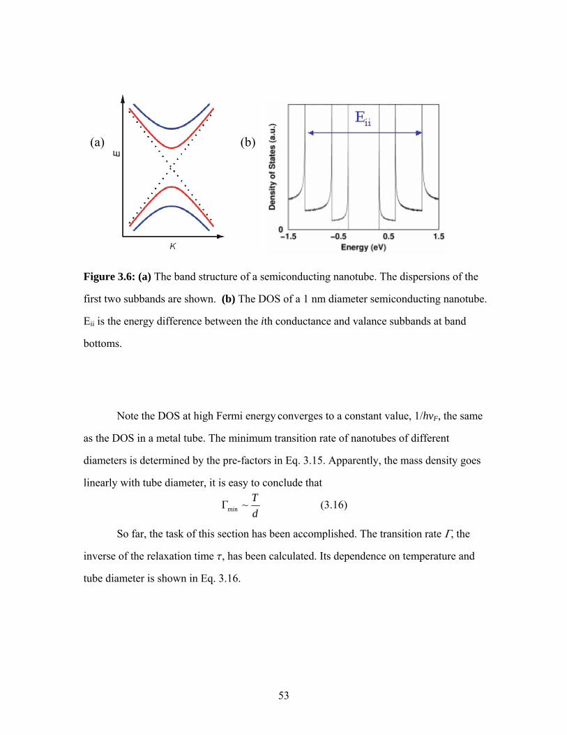
53
Figure 3.6: (a) The band structure of a semiconducting nanotube. The dispersions of the
first two subbands are shown. (b) The DOS of a 1 nm diameter semiconducting nanotube.
Eii is the energy difference between the ith conductance and valance subbands at band
bottoms.
Note the DOS at high Fermi energy converges to a constant value, 1/hvF, the same
as the DOS in a metal tube. The minimum transition rate of nanotubes of different
diameters is determined by the pre-factors in Eq. 3.15. Apparently, the mass density goes
linearly with tube diameter, it is easy to conclude that
dT~minΓ (3.16)
So far, the task of this section has been accomplished. The transition rate G, the
inverse of the relaxation time t, has been calculated. Its dependence on temperature and
tube diameter is shown in Eq. 3.16.
(b) (a)
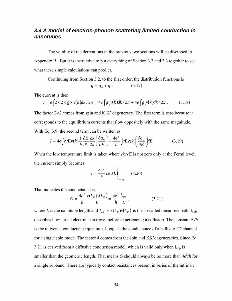
54
3.4 A model of electron-phonon scattering limited conduction in nanotubes
The validity of the derivations in the previous two sections will be discussed in
Appendix B. But it is instructive to put everything of Section 3.2 and 3.3 together to see
what these simple calculations can predict.
Continuing from Section 3.2, to the first order, the distribution functions is
10 ggg += . (3.17)
The current is then ( ) ( ) ( ) πππ 2/42/42/22
10dkkvgedkkvgedkkvgeI ∫∫∫ +=×××= . (3.18)
The factor 2µ2 comes from spin and K,K’ degeneracy. The first term is zero because it
corresponds to the equilibrium currents that flow oppositely with the same magnitude.
With Eq. 3.9, the second term can be written as
dEEg
kvhe
Egdk
kEkveeI ⎟
⎠⎞
⎜⎝⎛
∂∂
=⎟⎠⎞
⎜⎝⎛
∂∂
∂∂
= ∫∫ 02
0 )(42
1)(4 EE τπ
τh
. (3.19)
When the low temperature limit is taken where ∑g/∑E is not zero only at the Fermi level,
the current simply becomes
( )Fkk
kvheI
=
= Eτ24 . (3.20)
That indicates the conductance is
( )L
lhe
Lkvk
heG mfpFF
22 4)(4==
τ , (3.21)
where L is the nanotube length and ( )FFmfp kvkl )(τ= is the so-called mean free path. lmfp
describes how far an electron can travel before experiencing a collision. The constant e2/h
is the universal conductance quantum. It equals the conductance of a ballistic 1D channel
for a single spin mode. The factor 4 comes from the spin and KK’degeneracies. Since Eq.
3.21 is derived from a diffusive conduction model, which is valid only when lmfp is
smaller than the geometric length. That means G should always be no more than 4e2/h for
a single subband. There are typically contact resistances present in series of the intrinsic

55
resistance of the conduction channel. The observed G will always be smaller than 4e2/h in
that case.
Eq. 3.21 shows the value of G grows linearly with the mean free path. lmfp can be
calculated from the knowledge we already have. v(kF) is determined by the band structure.
With the simplified version of dispersion relation in Eq. 2.30,
( )( )2
0
2
00
2 F
FF
kvEg
kvvkv
h
h
+⎟⎠⎞
⎜⎝⎛
= . (3.22)
Here v0 is the Fermi velocity of a metallic tube, or the slope of the Dirac cones of a
graphene sheet. From Section 3.3, it is known that G(k) goes linearly with the density of
states at the Fermi level. In a 1D system, 1~
2−=== v
dEdkL
dEdk
dkdN
dEdNDOS
π. (3.23)
So the relaxation time t, the inverse of transition rate G(k), is linearly proportional to
v(kF). If we define t0 as the relaxation time when Fermi level reaches the linear
dispersion regime, then
00
)( ττvvk F
F = . (3.24)
When Eqs. 3.22 and 3.24 are plugged into Eq. 3.21, the conductance becomes
( )
( )2
02
20
2
2000
2
321
14
2
4
⎟⎟⎠
⎞⎜⎜⎝
⎛+
=
+⎟⎠⎞
⎜⎝⎛
=
FF
F
dk
Ll
he
kvEgkv
Lv
heG
h
hτ. (3.25)
It only depends on the position of the Fermi level. kF is determined by the number of
electrons in the tube. In our experiment, this is controlled through a gate placed next to
the tube with a dielectric layer in between (Fig. 3.1b). Define C’g as the gate capacitance
per unit length and assume the threshold voltage, where the Fermi level is at the bottom
of the first subband, is zero, then
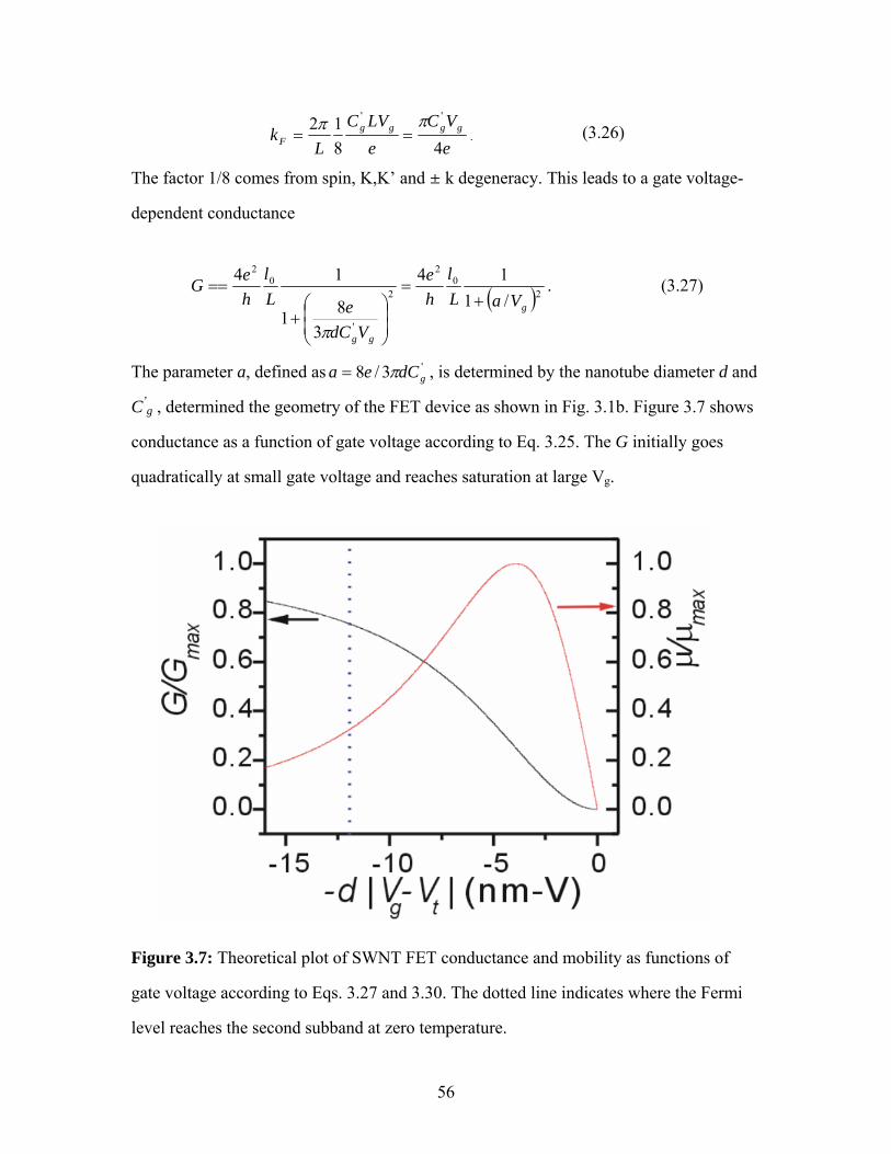
56
eVC
eLVC
Lk gggg
F 4812 '' ππ
== . (3.26)
The factor 1/8 comes from spin, K,K’ and ≤ k degeneracy. This leads to a gate voltage-
dependent conductance
( )20
2
2
'
02
/114
381
14
g
gg
VaLl
he
VdCeL
lheG
+=
⎟⎟⎠
⎞⎜⎜⎝
⎛+
==
π
. (3.27)
The parameter a, defined as '3/8 gdCea π= , is determined by the nanotube diameter d and
C’g , determined the geometry of the FET device as shown in Fig. 3.1b. Figure 3.7 shows
conductance as a function of gate voltage according to Eq. 3.25. The G initially goes
quadratically at small gate voltage and reaches saturation at large Vg.
Figure 3.7: Theoretical plot of SWNT FET conductance and mobility as functions of
gate voltage according to Eqs. 3.27 and 3.30. The dotted line indicates where the Fermi
level reaches the second subband at zero temperature.

57
Besides conductance, people typically characterize a conductor with a few other
quantities. One of them is electron (or hole) mobility m, which relates the electron drift vd
velocity to the applied electrical field: Evd /=µ . This quantity is, typically, a function
of the Fermi energy in microscopic semiconductors. In microscopic two dimensional and
one-dimensional semiconductors the Fermi level can be drastically changed by external
gates. A quantity called field effect mobility can be defined as
ggFE dV
dGCL
'=µ . (3.28)
From Eq. 3.27, the field effect mobility of a nanotube is
( )( )22
0'
/1
/3
aVg
aVghedl
dVdG
CL
ggFE
+==
πµ . (3.29)
The factor, 3pedl0/h, can be related to the effective mass at the bottom of the first
subband as derived in Section 3.2: m*= h/3pdv0. Then the formula can be rewritten as
( )( )22
0
/1
/
aVg
aVgme
FE+
= ∗
τµ . (3.30)
It is clear that mFE is a sensitive function of gate voltage Vg. When gate voltage is
barely above the threshold, the relaxation time of electrons (or holes) and their velocity
increase dramatically. At very high gate voltage, the Fermi level is in the linear
dispersion regime where the conductance is not changing anymore even though more
electrons are being added into nanotubes. This causes the field effect mobility to decay to
zero. There is a maximum point in between. Its position can be extracted from Eq. 3.30
with some simple algebra. When 3/aVg = , the maximum mobility is
∗∗ ≈=me
me
peak00 32.0
1633 ττ
µ . (3.31)
Section 3.3 also tells us that in the diffusive regime, the relaxation time and the
mean free path, depends on temperature as well as diameter. From Eq. 3.16 we can write

58
dTατ =−1
0 , (3.32)
where a is a proportional factor. When Eqs. 3.27, 3.31 and 3.32 are combined, the
maximum conductance and peak mobility for a nanotube with diameter d at temperature
T is
;48.02
0
Td
hev
peak αµ =
Td
Lhve
Gα
02
max4
= . (3.33)
In conclusion, in the previous three sections, a model based on the relaxation time
approximation is derived for electron-phonon scattering in nanotubes in the diffusive
regime. It gives predictions on how conductance and mobility change in nanotube with
respect to the Fermi level/gate voltage. These results will be compared with experimental
data in Section 3.5.
3.5 Comparing data with theory
The experimental observations in Section 3.1 agree with the theory predictions of
Section 3.4, at least qualitatively. On single device level, the measured conductance as a
function of gate voltage in Fig. 3.2 looks quite similar to the theoretical plot in Fig 3.7.
On the ensemble level, Fig. 3.4 shows that both resistivity and mobility of nanotubes
depend strongly on diameter, but in different ways: 1/Ron ~ d and µ ~d2. This agrees
with Eq. 3.33. The observed linear temperature dependence of resistivity and µ-1 is also
predicted by the same equation.
To be more quantitative, from the data in Fig. 3.2 we can extract values for the
coefficient a from either the maximum conductance or the peak mobility:a = 9.2 mK-1s-1
and a= 12 mK-1s-1. A group at University of Maryland (Pennington and Goldsman 2003)
obtained a value of α ≈ 6.5 mK-1s-1 for the total scattering rate in their theory calculations.
More recently, using Monte Carlo simulation, an IBM group (Perebeinos et al. 2005)
obtained nearly identical function forms to Eq. 3.33 but with a smaller value a ≈ 1.6 mK-

59
1s-1. In general, theory calculations predict better conductance and mobility in nanotubes
than what are observed in this experiment and in a recent experiment from a Columbia
group (Purewal et al. 2007). The origin of this discrepancy may come from the lack of
knowledge of the deformation potential D value. In a recent study, a theory paper
(Pennington et al. 2007) fitted the data in Fig. 3.2-3.4 and found out the best value for D
is 14 eV, which is close to the value in graphene (16 eV).
In conclusion, SWNT FETs were studied in the diffusive regime in this chapter.
The on-state conductance increases linearly with the tube diameter d, and the peak
mobility grows as d2. Both quantities grow linearly with T-1. These observations are in
good agreement with the predictions for scattering by low-energy phonons coupled with
the 1D “relativistic” band structure. These results set the ultimate performance limits of
SWNT transistors operating in the diffusive regime.

60
CHAPTER 4
INTRODUCTION TO CELL MEMBRANES
From this point on, this thesis will focus on biology inspired researches. Biology
may well be the most rewarding research area of this century. Unlike physics, where
people can understand most phenomena based on a few fundamental principles and
logical reasoning, biology, at least as of today, seems more complicated and is without a
grand theory. This is because in biology everything is correlated to a certain level and ‘a
single particle’ view is not feasible. Life is more complex than anything human beings
have ever designed, such as computers, rockets and photolithography steppers.
Modern biology was studied mostly from the chemistry perspective in the
beginning. But physics is needed to understand many phenomena in life. For example,
normally the most essential knowledge about a molecule is its chemical formula. But
because many biomolecules are large in size, their conformations, which are strongly tied
together with their functionalities, are governed by physics laws. Another example is
physics laws also describe how biomolecules move around. Physicists also provide new
tools/instruments to expand biologists’ experimental capabilities, such as better
visualization of molecule structures or sorting cells/molecules. That is why biophysics
has emerged as an active research area.
Chapter 5 will describe our research on integrating nanotubes with cell
membranes. Since cell membranes have many unique properties that are not well known
to the physics community, this chapter is dedicated to a brief introduction on membranes.
The physical and chemical properties of the basic components of cell membranes, lipids
and membrane proteins, will be discussed. The motivation and advantages of forming
artificial membranes will also be provided together with some experimental techniques.

61
4.1 Lipids and membrane proteins form cell membranes
Figure 4.1 illustrates a patch of cell membrane based on the Mosaic model. Cell
membranes are mostly made of two major components: lipids and membrane proteins. In
the Mosaic model, the lipid bilayer makes up the backbone of the membrane, where
proteins are sparsely distributed and free to diffuse. Not surprisingly, this early-
established simple model did not capture many essential properties of cell membranes.
The weight percentage of membrane proteins in cell membranes, it turns out, is
significant and the protein mobilities are controlled by the cells in a way yet to be
understood. However since this thesis deal with simple model membrane systems, most
discussions will be on the level of this Mosaic model. A few of the most important
properties of lipids and membrane proteins will be introduced in this section.
Figure 4.1: Schematic of a patch of cell membrane (library.thinkquest.org).

62
Lipids, one type of amphiphilic molecules
Most salts (ionic crystals) can dissolve in water. But for other small molecules
that are made of a few atoms, some of them can dissolve in water while others cannot.
Water is a polar solvent due to its intrinsic electrical dipoles. Just like in human society
where people like to spend time with friends of similar characteristics, polar molecules
are soluble in water while non-polar molecules are not. Hydrophilic and hydrophobic are
used to categorize molecules into two flavors.
However, there is another category. When molecules become large, they can have
segments that have intrinsic dipoles or charges while other segments that do not. Figure
4.2 shows a molecule, commonly used in detergents, called sodium dodecyl sulfate
(SDS). The head group around the sulfur atom becomes ionic in water solution, and is
thus hydrophilic. Each line in the zigzag part denotes an individual -CH2 group. Since the
bonding electrons in -CH2 groups have similar affinity to both carbon atom and hydrogen
atom, this part is non-polar. The zigzag part can be considered as a hydrophobic tail
group. SDS belongs to a group of so-called amphiphilic molecules. The head group does
not have to be ionic like in the case of SDS, an intrinsic dipole is enough to interact
strongly with water. Figure 4.3 shows a lipid molecule, called 1,2-Dioleoyl-sn-Glycero-3-
Phosphocholine (DOPC), that has a dipole in the head group. It should also be noted that
DOPC has two hydrocarbon chains instead of one. DOPC will be of great interest in
Chapter 5.
Figure 4.2: Structure of SDS molecule (Wikipedia).

63
Figure 4.3: Structure of DOPC molecule (Avanti Polar Lipids).
Assembly of amphiphilic molecules
Amphiphilic molecules may dissolve both in water and non-polar solvents, e.g. oil.
However their conformations could be different in different solvents. When the
concentration is not too low, they can assemble into many interesting structures.
When one SDS is put into a bucket of water, the hydrophobic tail group cuts the
hydrogen bond network of the water molecules. In other words, a surface energy must be
paid. The interfacial free energy of saturated hydrocarbon water interface is about 50
mJm-2 (Israelachvili 1991). This value is smaller when unsaturated C=C bonds are present.
When two SDS molecules are put into solution, they would like to have the tail groups
next to each other so that the total surface area is reduced. However, entropy keeps them
away. When the SDS concentration reaches above a threshold level, they can finally
assemble into the micelle structure shown in Fig. 4.4. In micelles, the hydrophobic tail
groups of SDS are wrapped inside the hydrophilic head groups to keep them away from
the water. Thus it is in an energetically favorable configuration. Amphiphilic molecules
can be used as surfactants. For example, SDS is used to wrap around nanotubes to
disperse them in water solution (O'Connell et al. 2002).

64
Figure 4.4: Schematic of a micelle structure (answers.com).
Figure 4.5: Schematic of a bilayer vesicle structure (Barrett group, McGill University).

65
When many DOPC molecules are dissolved in solutions, they form a different
structure as shown in Fig. 4.5. The DOPCs assemble in a tail-to-tail bilayer fashion and
form vesicles with a cavity inside. This lipid bilayer structure already looks like a cell
membrane.
The self assembly is determined by interactions between the amphiphilic
molecules and the water. Apparently there is a repulsive force between the polar head
groups. The force between tail groups is attractive due to Van der Waal interaction and
hydrophobic effects in water. To make a stable structure, the areas occupied by the head
group and tail group will be at values where the total free energy is minimized. These two
values do not have to be the same.
When all the complicated forces are put aside, phenomenologically, the shape of
the self-assembled structure is governed by a dimensionless geometric factor called the
packing parameter: p = V/(aµlc), where a is the head group area, V is the volume of the
hydrocarbon tail group and lc is the critical length of the hydrocarbon chain. lc is the
maximum length the chain can extend while still being fluid, and is on the same order as,
but smaller than, the fully extended length. When p is less than 1/3 as in the case of SDS,
individual amphiphilic molecule is in the shape of a cone and they will form micelles.
When p is larger than 1/3 but smaller than 1 as in the case of DOPC, the molecules are
analogous to truncated cones and they form either cylindrical micelles or bilayer vesicles.
When p is around 1, the molecules are in the shape of a cylinder and they form planar
bilayers (Israelachvili 1991).
This packing parameter is not strictly an intrinsic property to the amphiphilic
molecules. The solvent, water in this case, plays the important role. The strength of the
electrostatic repulsion between head groups is mediated by ions in the water solution. For
example, SDSs form micelles in low salt buffer. But when the ionic strength is increased,
the head group would like to stay closer and the effective area would decrease. That
makes the packing parameter go larger than 1/3 and they start to form cylindrical micelles.

66
Along the same line, introducing divalent ions like Ca+, which can be shared as
counterions by adjacent head groups, can also reduce the repulsion between head groups
and increase the packing parameter p.
Besides electrostatic effects, temperature can also change the optimal structure for
a given system. This effect is more subtle and difficult to predict. In general temperature
can modify the packing properties of the hydrocarbon chains. Increasing temperature can
make the hydrocarbon chain more mobile and reduce lc.
Another interesting method to change the self-assembly properties is by
introducing lipid mixtures. When two lipids are mixed together, assuming they do not
phase separate into different regions, each of them can still be described by its own
packing parameter. When one type of molecules with p < 1/3 is mixed with another type
with 1/2 < p < 1 at the right condition, they may form cylindrical micelles.
Permeability of lipid bilayers
Lipid bilayers are the central theme of this chapter. Mother Nature uses lipid
bilayers to form the backbone of cell membranes. Unlike rock solid walls, cell
membranes need to be permeable to certain molecules because cells need to get their food
from and send out their wastes to the outside world. Cells in multiple cellular organisms
need to communicate with others to coordinate their behaviors. The job of cell
membranes is to successfully control the traffic of various molecules and conduct signals
into and out of cells.
When there is a concentration difference of a certain molecule across a bilayer,
the molecules will try to permeate through the bilayer to equilibrate the concentrations on
the two sides. The permeability P, defined as P = j/Dc where Dc is the concentration
difference and j is the flux density, is obviously molecule dependent. A similar

67
permeability will be discussed in Chapter 5 to characterize the lateral diffusion and
diffusion hindrance of lipids and proteins inside lipid bilayers.
Let us first ponder on how molecules can go through a bilayer membrane. They
first need to leave the aqueous solution to enter the hydrophobic zone in the middle of the
bilayer. Then they need to diffuse through this zone and come out on the other side. The
first quantity that influences P is how much the molecule prefers the hydrophobic oily
environment compared to water. This is quantified by a parameter called the partition
coefficient B. Suppose a test tube is filled with water and a hydrophobic solvent such as
octanol. When a small amount of these molecules is added into the test tube, after
complete mixing, the ratio between the molecular concentrations in the hydrophobic
solvent and in the water equals the dimensionless partition coefficient B. Besides that, P
is also proportional to how fast the molecules can move around in the hydrophobic zone.
In short, P is proportional to BµD with D being the diffusion coefficient in oil for each
specific molecule. This has been verified experimentally in the 1980s by the Finkelstein
group (Orbach and Finkelstein 1980). Figure 4.6 is the original plot in their publication.
Although the ten different molecules have quite distinct permeabilities, they all fall onto a
line that shows the proportionality between P and BµD. In general, small gas molecules
and hydrophobic molecules have a high permeability. Even small polar molecules like
water and ethanol can penetrate the membrane. But large polar molecules, such as
glucose, and charged molecules of any size, such as Na+, cannot.
This tells us that cell membranes cannot be made of lipid bilayers only. Cells will
starve to death because food cannot go through the bilayers in this passive transport mode.
Luckily nature designs cell membranes with many proteins that sit in the bilayer to
facilitate transport of molecules with or without the cost of energy consumption.

68
Figure 4.6: Permeability as a function of B times D (Orbach and Finkelstein 1980).
Membrane proteins
Membrane proteins can be categorized by the way they associate with
lipid bilayers. A transmembrane protein, one that spans the whole lipid bilayer, has both
hydrophilic region and hydrophobic region. The end result is part of the protein likes to
sit inside the bilayer while others want to be immersed in aqueous solution. This type of

69
Figure 4.7: Different types of membrane proteins (www.geneontology.org).
Figure 4.8: Two examples of transmembrane proteins: potassium channel (left)
(www.steve.gb.com) and hemolysine (right) (molbiol.ru).

70
proteins is shown on the right side of Fig. 4.7. Another type of proteins anchors to
membranes by making covalent bonds with the lipids, shown in the middle of Fig. 4.7,
and they are called integral proteins. The last type attaches to other molecules in the
membrane by weak electrostatic, hydrophobic and other non-covalent interactions and
can be release from the membrane; these are called peripheral proteins.
Obviously, only transmembrane proteins are capable of transporting molecules
across the bilayers. There is a whole zoo of transmembrane proteins. One of the brightest
stars is the potassium ion channel shown on the left side of Fig. 4.8. The structure of the
potassium ion channel was determined with protein crystallography by Prof. MacKinnon
of Rockefeller University (Doyle et al. 1998), which won him the 2003 Nobel Prize in
Chemistry. Another one in current spotlight is a-hemolysine (Mathe et al. 2005), as
shown on the right side of Fig 4.8, which can let single strand DNAs go through
membranes. The holes in the transmembrane proteins that allow molecules to pass
through are visible in this figure. The difference between the two types of proteins shown
in Fig. 4.8 is that the potassium ion channel can be gated to be either open or closed while
a-hemolysine has just a passive opening. Artificial nanometer scale solid state pores have
recently been fabricated (Dekker 2007) to simulate a-hemolysine. They show promise for
several applications including DNA sequencing.
The purpose of other types of membrane proteins will not be discussed. But an
important fact about membrane proteins is that transporting molecules is not their sole
job. They do not necessarily have holes as potassium ion channel and a-hemolysine.
Membrane proteins can also conduct signals in other ways. For example, when a
compound binds to part of a transmembrane protein on one side of the membrane, it can
generate conformational changes in the transmembrane proteins to trigger a series of
chemical events on the other side of the membrane. This example also indicates that the
functions of these proteins are regulated by many methods, including ligand binding in
this case and electrical potential in other cases.

71
Transmembrane proteins are hard to study because they require bilayers to keep
their correct conformations, and many of them do not dissolve in water (thus are hard to
crystallize). That is why their structures were determined much later compared to other
proteins. This also makes people interested in forming artificial bilayers to provide
playgrounds for membrane proteins, which will be discussed in Section 4.2.
Diffusion in membranes
One important property of lipids and membrane proteins in cell membranes can
be seen from one experiment. Figure 4.9 is a schematic of a well known experiment in
1970 (Frye and Edidin 1970) in which human cell and mouse cell were fused together
and the human/mouse proteins mixed on the surface of the new entity (Yes, crazy
biologist!). It proves that membrane proteins, lipids as well, are not static. Instead, they
are moving around laterally in cell membranes
Figure 4.9: Schematic of the cell fusion experiment (Frye and Edidin 1970). The
membrane proteins from the two cells mixed uniformly within an hour.

72
The lateral diffusion of lipids and protein in the membrane is an important process
yet to be fully understood. To the first order, it can be modeled as two-dimensional
random walk. The mean square displacement in a two-dimensional diffusion increases
linearly with time : <(xN)2> = 4Dt, where D is the diffusion constant.
Lipid diffusion is simpler than protein diffusion due to their small sizee, and it
follows the random walk model most of the time. The typical lipid diffusion coefficients
are around ~mm2/s. But there are exceptions. Each lipid species has a characteristic
transition temperature. Below it interactions between the lipid tail groups are so strong
that the lipids are tied together in a gel fashion. This makes the diffusion limited. When
lipids with different transition temperature are mixed, they may phase separate out
making so-called lipid rafts. The lipid raft model (Brown and London 1998) is proposed
to describe the phenomenon where a mixture of different lipids/proteins are effectively
bundled up and diffuse together.
Membrane proteins can diffuse quickly in random walk fashion in artificial lipid
layers. In real cells, however, the behaviors of membrane proteins typically cannot fit
with the random walk model. Their diffusion coefficients can vary drastically. Cells have
the ability to confine them to certain spots on the membrane. This will be discussed
further in Chapter 5.
Lipid bilayer fusions
Another noticeable process in the experiment illustrated in Fig. 4.9 is that cells
can fuse. In general when two lipid bilayer vesicles are put against each other at the right
condition, they can integrate into one. These fusions are typically facilitated by
membrane proteins in real life.
Lipid bilayers fusion happens so often that it is used as another mechanism for
molecule and signal transports across membranes, through a process called exocytosis.

73
One example, the complex synapse process, is shown in Fig. 4.10. For the purpose of
this section, one only needs to focus on how neurotransmitters, the green triangles in Fig.
4.9, are excreted out via vesicle fusion with the cell membrane. These neurotransmitters
are initially wrapped inside synaptic bilayer vesicles floating in the cytoplasm of the
nerve terminal. When these vesicles fuse with the cell membrane of the neuron,
neurotransmitters are exposed and released to the synaptic junction. The event is
propagated to the cell on the bottom when the neurotransmitters bind to the receptors on
its membrane. Exocytosis exists in cells other than neurons too, and is widely used to
dump waste or signaling molecules.
Figure 4.10: Schematic of synapse processes that require lipid bilayer fusions
(CNSforum.com).

74
In summary, this section presents a few characteristics of cell membranes and
their components. An important method to study these properties is going to be
introduced in the next section.
4.2 Artificial lipid bilayers
Real cell membranes are not easy to study. For example, a popular yet notoriously
hard method used to study the transport behavior of ion channels is patch clamp method
(Hamill et al. 1981). It requires using a micrometer sized pipette tip to make a well-sealed
contact to a small patch of fragile membrane without breaking it. It is not easy to keep
cells healthy and happy, especially for physicists.
As in most biology experiments, fluorescence microscopy is used as a powerful
tool to study cell membranes. But sometimes it is difficult to eliminate the background
light coming from the cell bodies. For example, the imaging is very challenging when
fluorescence microscopy is used to visualize the processes happening at the cell-cell
junctions.
Most importantly, cell membranes are complex systems, typically composed of
many types of lipids and a large number of proteins of different purposes. This makes it
very difficult to study the properties of a single component.
This is why people invented a few model membrane systems using lipid bilayers.
These membrane mimics have various experimental advantages while capturing the
essence of cell membrane. The artificial membranes are typically stable and can be used
with many sophisticated imaging and electrically techniques. It is much easier to study
single protein or process one by one with model membranes since their compositions are
well controlled. Artificial membranes can be integrated with other organic and inorganic
structures and could produce many medical applications, besides their significance in
scientific research.

75
Here, a few types of artificial lipid bilayers will be discussed. They each have
their own merits and drawbacks.
Suspended lipid bilayer
One way to form a small area lipid bilayer is by using sable hair brush to paint
lipids (Akeson et al. 1999; Bernards et al. 2006) on a small aperture that connects two
chambers. After the chambers are filled with buffer solution, a fine brush is used to put a
small droplet of organic solvent with lipid molecules onto the aperture. After the solvent
evaporates, a suspended lipid bilayer, sometimes called black membrane, is assembled
across the aperture. Figure 4.11 shows the apparatus and resulting lipid bilayer. The
formation of the bilayer is monitored by measuring the junction resistance and
capacitance.
Figure 4.11: One example of suspended lipid bilayers (Akeson et al. 1999).

76
Another way to form a suspended lipid bilayer in this same two-chamber
configuration can be done without using brushes. First, one of the two chambers is filled
with oil and the other with water. When lipids are put into water, they will form a
monolayer at the aperture between water and oil to reduce the surface energy. This
aqueous lipid solution can then be introduced into the oil chamber to gradually replace all
the oil. Once the water oil interface reaches the aperture, another monolayer will form
against the original one to make a bilayer.
Suspended model membranes provide an excellent system to study transport
processes through bilayers. For example, a-hemolysine can be inserted to a patch of
suspended membrane and DNA translocation through the protein can be studied by
monitoring the reduction in conduction through the protein pore (Mathe et al. 2005). The
lifetime of this type of artificial membrane is on the order of hours, and is sufficiently
long for most purposes. This type of model membrane does not have particular imaging
advantage though.
Supported lipid bilayer
Another kind of model system that is becoming more popular is called supported
lipid bilayers (SLBs), shown schematically in Fig. 4.12. It is basically a two-dimensional
lipid bilayer sitting on top of a flat and hydrophilic solid substrate such as glass, mica and
oxidized silicon wafers.
SLBs are typically formed through vesicle fusion and rupture. Lipid molecules
first self assemble into vesicles. When a droplet of this vesicle solution is put on a flat
hydrophilic substrate, the vesicles will stick to the substrate and from a two-dimensional
lipid bilayer sheet (detailed experimental methods in Chapter 5). This transition process
was studied carefully by the Boxer group at Stanford (Johnson et al. 2002). When a

77
Figure 4.12: Side view of a patch of support lipid bilayer.
Figure 4.13: Forming SLBs via vesicle fusion and rupture (Johnson et al. 2002).

78
vesicle is attracted to a substrate due to interfacial forces (this is why it only works on
hydrophilic substrates), another vesicle floating in the solution can fuse with the one
stuck on the substrate to form an American-football shaped cylindrical vesicle. The
membrane curvature is reduced in the fusion process. And eventually these bigger
vesicles rupture to form planar membranes. Figure 4.13 shows this process in a pictorial
way. There are other mechanisms for this transition process, but the one shown in Fig.
4.13 is the main route. This implies that the transition from vesicles into SLBs is easier
with high concentration vesicle solutions since it requires interactions and fusion between
multiple vesicles.
Advantages of SLBs
One of the biggest advantages of SLBs’ is that they serve as a versatile imaging
platform because the membrane is flat and sitting on microscope compatible substrates.
For example, it is used as a model system to study membrane interactions between two
cells. This is hard to do in other systems since they require sophisticated manipulation of
cells and elimination of unwanted background light. The Groves group (Mossman et al.
2005) used a flat SLB and a vesicle to simulate this process. The membrane-membrane
junction is easy to form in this case. Total internal reflection technique, which relies on
the evanescence light waves that can only penetrate a small depth (~100 nm) into samples
of interest when total internal reflections happen, is used to illuminate only a thin layer of
space around the membrane junction to get rid of background noise. Another microscopy
that can be used with SLBs is fluorescence interference contrast microscopy, which can
be used to acquire nanometer scale height variation information. The Groves group
(Parthasarathy et al. 2006) made SLBs on top of SiO2/Si wafers. Both the excitation and
fluorescence emission from the membrane interfere with the reflections from the nearby
silicon surface. Therefore the intensity of the fluorescence signal is a sensitive function of
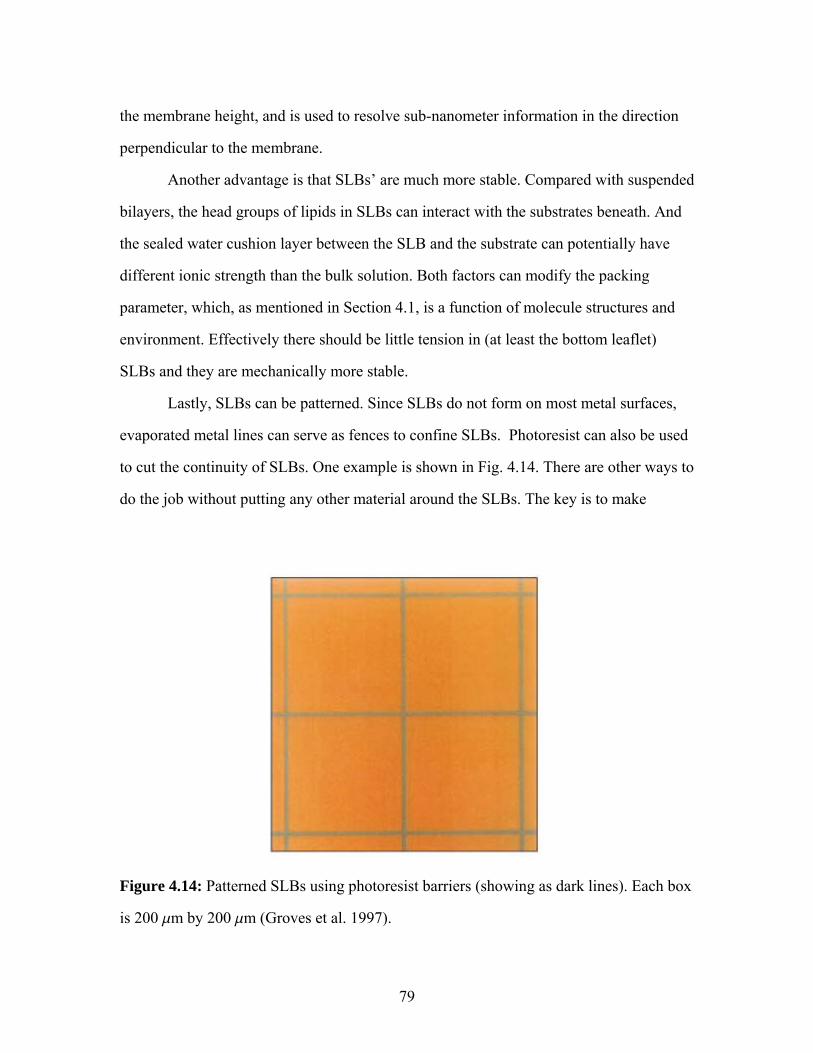
79
the membrane height, and is used to resolve sub-nanometer information in the direction
perpendicular to the membrane.
Another advantage is that SLBs’ are much more stable. Compared with suspended
bilayers, the head groups of lipids in SLBs can interact with the substrates beneath. And
the sealed water cushion layer between the SLB and the substrate can potentially have
different ionic strength than the bulk solution. Both factors can modify the packing
parameter, which, as mentioned in Section 4.1, is a function of molecule structures and
environment. Effectively there should be little tension in (at least the bottom leaflet)
SLBs and they are mechanically more stable.
Lastly, SLBs can be patterned. Since SLBs do not form on most metal surfaces,
evaporated metal lines can serve as fences to confine SLBs. Photoresist can also be used
to cut the continuity of SLBs. One example is shown in Fig. 4.14. There are other ways to
do the job without putting any other material around the SLBs. The key is to make
Figure 4.14: Patterned SLBs using photoresist barriers (showing as dark lines). Each box
is 200 mm by 200 mm (Groves et al. 1997).

80
different regions of the substrate surface with different properties. One method (Moran-
Mirabal et al. 2005) involves covering regions where SLBs are not needed with thin
parylene film before the substrate is exposed to vesicle solutions. After a SLB is formed
on the substrate, parylene film can be peeled off to leave SLB patches at regions of
interest. With both techniques, the SLB patterns can be defined down to micrometer scale.
Lipid mobility in SLBs
One may worry that the lipid mobility in SLBs is degraded due to the presence the
nearby solid substrates. But since the attractive force is small, the lipids are still diffusive
in SLBs. The diffusion coefficient can be measured accurately with Fluorescence
Correlation Spectroscopy (FCS) (Moran-Mirabal et al. 2005) or Fluorescence Recovery
After Photobleaching (FRAP). Detailed discussions can be found in Section 5.2. It is hard
to compare the lipid mobility in SLBs to that in real cells since cell membranes are made
of complicated mixtures of lipid varieties and membrane proteins. However the diffusion
coefficient is on the same order.
The lipids in SLBs can be manipulated with external forces. In one experiment, a
charged lipid species is mixed with another neutral type in an SLB (Groves et al. 1996).
They do not phase separate under normal conditions. When an in-plane electrical field is
applied, however, the negatively charged lipids start to move under the influence. The
distribution function is a result of the competition between the electrical potential and
thermodynamic equilibration. As Fig. 4.15 shows, the negatively-charged fluorescence
lipids, red in color, build up at the edges of SLB corrals opposite to the direction of the
electrical field lines. In Chapter 5, we will show another example where proteins
attached a SLB are manipulated by fluid flow.

81
Figure 4.15: Driving charged lipid molecules in SLBs with electrical field (Groves et al.
1996).
Protein mobility and polymer supported lipid bilayer
As mentioned before, membrane proteins can be integrated into SLBs in order to
study their properties. But the mobility of membrane proteins can be degraded due to
their interaction with the substrates. This is because proteins are large. When part of the
proteins extruding from the SLBs strongly interacts with the substrate, they will be
pinned. On top of that, the protein may denature, or change their conformations in other
words, to lose their normal functionalities. There are a few methods to solve this
difficulty (Sackmann 1996). First, when the extruding parts are not essential to protein
functions, they can be chopped off. For example, if a protein only serves as receptors to
other molecules, there are only two parts needed to remain intact: the group in charge of
recognition and binding and the group that anchors the protein to lipid bilayers.
In the case of other more complicated transmembrane proteins like ion channels,
however, the structure cannot be altered. Then the solution to the mobility and

82
denaturation problems can be solved by adding a hydrated polymer cushion layer
(Sackmann 1996) between the lipid bilayer and the substrate as shown in Fig. 4.16. This
is actually a better mimic of cell membranes. Cells in multi-cellular organisms are
surrounded by an extracellular matrix, which is essentially made of biopolymer meshes.
Because of that, proteins are expected to perform their functions in polymer supported
bilayers.
Experimentally it may be a little more difficult to functionalize the substrates with
a flat polymer layer and then form bilayers on top. Another possible solution is to use
small percentage of lipids with very large head groups when constructing the bilayer. The
hope is that these lipids will act as pillars to push the bilayer further away from the
substrate to prevent proteins from interacting with the substrate. As far as the author
knows, this idea has not been tried or has not been successful enough to be reported.
Figure 4.16: Schematic of polymer supported lipid bilayers (Sackmann 1996).

83
In summary, a brief introduction to amphiphilic molecules, cell membranes and
lipid bilayers are given in this chapter. Artificial membranes, including SLBs, are shown
to be flexible platforms to study membrane properties. This knowledge is indispensable
for the experiments in the next chapter.

84
CHAPTER 5
SUPPORTED LIPID BILAYER/CARBON NANOTUBE HYBRID
Single-walled carbon nanotubes (McEuen 2000) (SWNTs) offer unique
opportunities for chemical (Kong et al. 2000) and biological sensing (Besteman et al.
2003; Star et al. 2003). In this chapter, we will present our research on integrating
SWNTs with artificial cell membranes for sensing protein binding events and studying
the interaction between nanotubes and lipids/proteins.
In Sections 5.2-5.5, we show the integration of supported lipid bilayers (SLBs)
(Brian and McConnell 1984; Sackmann 1996; Richard et al. 2003)with SWNT field
effect transistors (FETs). We first demonstrate membrane continuity and lipid diffusion
over the tube. We show that, however, the NT acts as a diffusion barrier for a membrane-
bound tetanus toxin protein, and that the strength of the diffusion barrier depends on the
diameter of the NT. Finally, we present results on the electrical detection of specific
binding of streptavidin to biotinylated lipids.
The formation of fluidic SLBs on SWNTs will allow the study of lipid-SWNT
interactions and sensing of analytes binding to specific receptors imbedded in the SLBs.
These studies should have an impact on our understanding of model and biological
membranes (Zhou et al. 2007).
But before the main content of the chapter, as a prelude, Section 5.1 is used to
discuss why people are interested in nanotube sensors, what people have accomplished
and why we chose to study cell membranes.

85
5.1 Prelude
Why is a nanotube an interesting component to interact with biomolecules?
In order for nanotubes to be used in any experiments with biomolecules, which
require water solutions to retain their normal functions, it is critical to show that
nanotubes can work in aqueous environment. This was demonstrated a few years ago
(Kruger et al. 2001; Rosenblatt et al. 2002).
Figure 5.1 plots the conductance of a nanotube FET in 0.1 M NaCl solution as a
function of solution potential. The detailed experimental method is explained in Section
5.2. When compared to similar curves where the Fermi level is controlled by a back gate
as in Chapter 3, Fig. 5.1 shows the nanotube can be turned on much faster in solution,
demonstrating the large capacitance between water and nanotubes (Rosenblatt et al.
2002).
Figure 5.1: The performance of a nanotube FET in 0.1M NaCl solution.
0.8 -0.8 0.0
0.0
0.2
Vwg (V)
G [4e2/h]

86
After these studies proved the possibility of nanotubes working in salty water
solutions, the first idea of integrating nanotubes with biology was the use of nanotube
FETs as sensors. Since most biological molecules are charged, when they bind to a
nanotube, the local electrostatic environment is altered, which may generate a
conductance change in the FET. In other words, the threshold voltage of the FET is
shifted. This is a general approach valid for all FETs, but using nanotubes FETs as the
key element has quite a few advantages that can be summarized in four s-words:
Small. First of all, SWNTs are small, even when compared with micro
biomolecules. The nominal diameter of a DNA double helix is 2 nm. SWNTs can be even
smaller than that in diameter. This advantage can lead to high (even single molecule)
sensitivity, high spatial resolutions and parallel operations. The high sensitivity can be
very important. The concentration of macro molecules of interest is amazingly low in
many cases. It would be great to have a small sensor that does not require too much
analyte to get the test done.
Surface. For an electrical charge based sensing scheme, it is desirable to put the
conducting channels close to the analyte in order to increase the electrostatic coupling. A
nanotube is perfect in the sense that all the atoms are on the surface. Another advantage is
there is only one conduction channel in nanotubes. In a typical traditional FET sensor,
there are conduction channels underneath the surface that give rise to a large background
noise. Having only one conduction channel on a nanotube surface can raise the sensitivity
even higher.
Stable. In traditional semiconductor FETs, it is not possible to expose the electron
conduction channels directly to the aqueous environment because the ions can penetrate
into the FETs and ruin them. A dielectric layer is needed to isolate FETs physically from
ions in the solution. That would inevitably reduce the electrostatic coupling. Since carbon
nanotubes are in such a chemically inert form, they will not react with ions even when
there is reasonable (less than 0.7 V) electrical potential between them, as shown in Fig.

87
5.1. In other words, ions and electrons in nanotubes are separated by a fence that is
impenetrable at low voltage. This maximizes the electrostatic coupling and leads to high
sensitivity.
Superior mobility. Besides coupling efficiency, another factor influencing the
sensitivity is transconductance. It describes the amount of conductance change as a
response to a doping level modulation, and is linearly proportional to the FET mobility.
Under the same Fermi level modulation, signals from FETs with higher mobility are large
in magnitude and more easily detected. The mobility of nanotubes, as mentioned in
Chapter 3, can reach more than 15,000 cm2V-1s-1 at room temperature (Zhou et al. 2005).
This value is more than a few times larger than that of crystalline silicon. However, it
could be a double-edged sword in some cases. When there is a significant contact
resistance, the signal on FETs with high mobility and low resistance may be
overwhelmed by noise imposed by contacts. However it is always possible to operate
nanotube FETs at low doping level with the right gate voltage to make the signal coming
from the sensing region stand out.
These properties of nanotube FETs result in an extraordinary sensitivity. The
sensitivity is given by signal to noise ratio. In our experiments, it is possible to
distinguish a threshold change as small as 2 mV at 1 KHz bandwidth (This value cannot
be improved much by decreasing the bandwidth because the dominating form of noise is
1/f noise.). The capacitance between liquid solution and a nanotube is estimated and
measured to be around 4 µ 10-10 F/m (Rosenblatt et al. 2002). That means a doping
change of as few as 5 electrons in a 1 mm nanotube FET can be sensed. This does not
necessarily mean that a detectable signal can be generated when 5 extra ions are put close
to a micrometer long nanotube FET though due to charge screening: the mobile ions in
electrolyte solutions can efficiently decrease the magnitude of electrostatic interactions.
Single electron sensitivity is possible when the nanotube conduction channel
length is further reduced. This unprecedented sensitivity will enable electronic-based

88
molecule detections to complement optical techniques currently used for the purpose. It
will make huge impact in research and applications if it can be made to work effectively
and reliably.
Previous biosensors made of nanotubes
The first studies using nanotubes as biosensors focused on DNA or protein
detection (Besteman et al. 2003; Star et al. 2003), based on the idea discussed above.
These works are important because DNA and proteins are the two most essential
components of life, and have been in the spotlight of modern biology. As the central
dogma of molecular biology says (Alberts et al. 2002), DNA carries the genetic
information from one generation to the next while proteins, made from the blue print
encoded in DNAs, perform all the functions to keep cells alive. (RNA is also needed in
the transcription and translation process to produce protein molecules.) The ability to
detect specific DNA sequences and proteins can generate huge clinical improvements, e.g.
faster diagnosis and potential disease prevention.
On the other hand, in these previous studies the biomolecules were almost treated
identically to any charged particles, making these projects less appealing to biologists.
Why do we choose to study cell membranes
There would be no life on Earth if there were only DNAs and proteins in the
world. Without compartmentalization, entropy would put everything into thermal
equilibrium and make the world featureless. It is membrane that forms playgrounds for
DNA and protein to function properly. Figure 5.2 is a schematic of a cell. First of all, the
cell is separated from its surroundings by its cell membrane. Even on the inside, different
organelles are isolated as individual units by membranes. These membranes control the
traffic of all kinds of molecules, including food, waste and signaling molecules, into and

89
Figure 5.2: Schematic of a cell (web.jjay.cuny.edu/~acarpi/NSC).
out of the cell. A cross membrane potential is also used in the photosynthesis process to
store solar energy into chemical bonds, and in the metabolism to release energy from
chemical bonds (Alberts et al. 2002; Nelson 2004). Membranes are indispensable units of
life. That is why this part of the thesis will study membrane properties using nanotubes as
a tool.
Specifically, we will work with SLBs. SLBs self-assemble from phospholipids on
flat, hydrophilic substrates like glass, and mimic many properties of cell membranes. The
lipids in a SLB are laterally mobile and many reconstituted membrane proteins embedded
in them remain functional (Salafsky et al. 1996; Mossman et al. 2005). Although it has
been shown that lipid bilayers can form on top of multi-walled carbon nanotubes (Ye et
al. 2005) or SWNTs coated with polyelectrolytes (Artyukhin et al. 2005), the nanotubes

90
in these experiments were not used as detection elements and the bilayers were not
supported on flat substrates. Another group has placed membrane patches on SWNT field
effect transistors (FETs) (Bradley et al. 2005), but no continuous SLBs were formed and
the measurements were carried out in dry condition. As will be shown in following
sections, our research, for the first time, integrated high quality SLBs with nanotube
FETs.
5.2 Forming SLBs on nanotube chips
Methods of forming and imaging SLBs
The phospholipid used for SLB formation was the zwitterionic 1,2-dioleoylsn-
glycero-3-phosphocholine (DOPC, Avanti Polar Lipids). Small unilamellar vesicles
(SUVs) were prepared as previously reported (Groves et al. 1996; Moran-Mirabal et al.
2005) . Lipids were dissolved in chloroform at the appropriate molar ratios for a final
concentration of 1mM, and allowed to mix. The solvent was evaporated under a dry
nitrogen stream, forming a uniform lipid film. The lipids were then resuspended in either
10 mM or 1 µM (working solution for electrical detection) PBS buffer (pH 7.4), and
allowed to rehydrate. Finally, SUVs were produced by point-probe sonication at 100
Watt for about 10 minutes, yielding vesicles 50-100 nm in size. When vesicles were
incubated on hydrophilic substrates above the transition temperature of the mixture, SLBs
formed spontaneously via vesicle rupture and fusion.
In experiments with chips containing SWNT FETs, polydimethyl-siloxane (Ng et
al. 2002) (PDMS) microfluidic channels with a typical cross section of 10×50 µm were
laid on top of SWNT FETs to confine liquid solution to the area proximal to the SWNTs
(Fig. 5.3a). The alignment was done manually on a home-built probe station. A low-
magnification long-working distance microscope was used to keep track of the features
on nanotube chips and PDMS stamps. The edges of PDMS stamps were attached to a

91
holder, made from two glass slides with spacing in between that were glued to another
slide. The PDMS staples can be moved in three dimensions by a micromanipulator, and
were laid down on facing nanotube chips once alignment was achieved.
Once the PDMS sealing was visually checked under microscopes, the holder was
removed and the channel was filled with vesicle solutions. This was done by putting a
droplet of vesicle solution in one of the open reservoirs, holes punched in the PDMS
stamps and connected to the ends of the channels. After an incubation of about 15
minutes to allow SLBs formation, the channels were flushed many times with working
buffer to remove excess vesicles. Putting chips with vesicle solutions into a hot moisture
oven can help the SLBs formation if the transition temperature of the lipids is above
room temperature.
To image SLBs, Lissamine-Rhodamine Red 1,2-dihexadecanoyl-sn-glycero-3-
phosphoethanolamine (LR-DHPE) (Molecular Probes) fluorophores were mixed with
phospholipids at 0.1% molar ratio. Images were obtained by using an upright Olympus
fluorescence microscope with a thermo-electrically cooled 12 bit CCD camera (Cooke).
Nanotube device fabrication and cleaning
The SWNT FET devices (shown schematically in Fig. 5.3a) were fabricated as
previously reported (Rosenblatt et al. 2002). Carbon nanotubes were grown by chemical
vapor deposition on silicon wafers with 500 nm oxide capping layer3. Using
photolithography, gold electrodes were defined on top of the SWNTs with 2-10 µm gaps
between source and drain electrodes. The nanotube growth yield was controlled so that
most transistors had one nanotube bridging the electrodes. To do better optical imaging,
devices were made on 170 mm cover slips as well.
3 The oxide thickness was intentional chosen, although not precisely tuned due to vendor limitations, to make the interference between lights reflected from the oxide surface and silicon surface constructive (Parthasarathy, R. and J. T. Groves (2004). Optical techniques for imaging membrane topography. Cell Biochemistry and Biophysics 41(3): 391-414.). In this way, the illumination and fluorescence intensity from fluorophores in the SLBs are maximized. We can use lower fluorophore concentration to do imaging.

92
Figure 5.3: Representation of the supported lipid bilayer/carbon nanotube hybrids. (a)
Schematic of the side view of a SWNT FET inside PDMS microfluidic channel. (b)
Scaled schematic of a carbon nanotube under DOPC bilayer. DOPC lipid molecules are
shown with two light green fatty acid chains. A toxin protein, represented in a ribbon
model, binds to a membrane-embedded ganglioside molecule that is shown with two dark
green chains. There is a thin water layer between SLB and substrate.
Figure 5.4: SLBs cannot form on as-made nanotube chips (left). Fluorescence image of
high quality SLBs is shown on the right as comparison. The SLB is confined inside a
microfluidic channel on the right half of this image.
100 µ m
100 µm

93
In the beginning, vesicles would not fuse on chips with nanotube devices. A
fluorescent image of typical initial results of attempting to form SLBs is shown on the
left side of Fig. 5.4. This can be compared to the right side of Fig.5.4 that shows a
fluorescence image of a continuous SLB film on a clean SiO2/Si wafer. The only things
left on nanotube chips in the left image were unfused vesicles and small patches of SLBs.
Long dose of light was used to bleach fluorophores inside a small region, the result of
which is the dark circle region on the left side of Fig.5.4. The fluorescence from this
region stayed low for very long time, proving that there are no SLBs on large scale and
the lipids are not mobile. This failure of SLBs formation is because the surface is
contaminated with organic photoresists and amorphous carbon during photolithography
and tube growth processes.
Wafers containing SWNT FETs were cleaned with room temperature piranha
solution (volume ratio 3:1 concentrated sulfuric acid/30% hydrogen peroxide) without
sonication for 3-5 minutes4 or in a UV-ozone cleaner for 90 seconds at 70°C to remove
residual contamination from processing and render the surface hydrophilic. The cleaning
procedures were developed to allow the formation of uniform, fluid SLBs, and were
tested to insure that they did not degrade the SWNT FET device performance. Most
devices survived the cleaning procedures and their electrical conductance did not change
by more than 20%.
Confirming SLBs quality by measuring lipids diffusion coefficients
To verify the quality of SLBs on nanotube chips after cleaning, two standards
were used. First, the SLBs should spread on the whole surface uniformly. This is
confirmed by a uniform fluorescence as shown on the right side of Fig. 5.4 where a SLB
4 It has been noted that washing the chips with organic solvents, e.g. acetone and methanol, immediately before piranha cleaning can result in the lifting-off of electrodes and destroying the FETs.

94
was formed inside a PDMS channel5. Another standard is that lipids should be able to
diffuse laterally within the SLBs. To test this, diffusion coefficients were measured and
compared to reported values from other groups.
This can be done with two methods. One method uses fluorescence recovery after
photobleaching (FRAP) technique. In these experiments fluorophores inside a circular
region with radius R are photo bleached at time t = 0, as shown in the left panel of Fig.
5.5. The fluorescence intensity I at the center recovers as the bleached fluorophores
diffuse away. The right panel of Fig. 5.5 shows a typical fluorescence recovery curve.
Since we use high intensity light to bleach all the fluorophores in the circle over a small
period of time, we assume all the fluorophores inside it are dead6 and consider the non-
zero intensity as background noise. Then we can define normalized fluorescence
intensity F as F = (I-I0)/I¶ , where I0 and I¶ are the fluorescence intensities at time 0 and
at infinite time.
In the case of two-dimensional isotropic diffusion, the probability for a particle
with diffusion coefficient D leaving the origin at time zero to be at distance r away from
the origin at time t is
DtDtr
trPπ4
4exp
),(
2
⎟⎟⎠
⎞⎜⎜⎝
⎛−
= . (5.1)
The fluorescence intensity inside the circle after bleaching should grow back
when the dead fluorophores diffuse away and fresh ones come in. The normalized
intensity of the center should be one minus the probability of any of the dead
fluorophores occupying that location
5 SLBs form on the channel walls of the PDMS stamps. When the fluorescence intensity was studied quantitatively as in this section and some other parts, the images were taken once the PDMS stamps were removed inside a beaker with buffer solution, leaving the SLBs on the substrates intact. Images in these cases were collected with a water immersion lens. Future experiments can use transparent substrate and total internal reflection microscopy to solve the background fluorescence issue if PDMS channels are indispensable. 6 This is an approximation as fluorophores are constantly diffusing in and out of the circle.

95
0 50 100 150 200 250 300 350 400 450 5000
2000
4000
6000
8000
10000
12000
0 100 200 300 400
-2.0
-1.5
-1.0
-0.5
0.0
1/ln
(F)
t (s)
I (A.
U.)
t (s)
Figure 5.5: Estimation of lipid diffusion coefficient using FRAP. Left panel:
Fluorescence image around the bleached region (dark circle in the center) at time 0.
Right panel: Fluorescence intensity at the center of the circle recovers over time. Inset:
Inverse log of the normalized fluorescence intensity plotted versus time.
∫ ⎟⎟⎠
⎞⎜⎜⎝
⎛−=
⎟⎟⎠
⎞⎜⎜⎝
⎛−
−=R
DtRrdr
DtDtr
F0
2
2
4exp2
44
exp1 π
π. (5.2)
By fitting the curve in the right panel of Fig. 5.5, we get t ~ 2µ 102 s. Since R ~
50 µm in the test, the diffusion coefficient of DOPC is D º 3 µ 10-8 cm2/s. This value
compares favorably with previous reports (Orth et al. 2003). This method is simple in
practice because it does not require complicated apparatus and can be applied to SLBs on
opaque substrates.
Another method is called fluorescence correlation microscopy (FCS). It records
the fluorescence intensity of a small volume and analyzes the fluctuations due to
molecule diffusion to reveal the dynamical information. In these experiments a
diffraction-limited illumination volume was obtained by filling the back aperture of the
objective. The illumination volume was calibrated by obtaining autocorrelation curves

96
from a freely diffusing molecule (Alexa488-dUTP) with known diffusion constant
(2.1×10⁻⁶ cm2/s) (Foquet et al. 2004). The calibration yielded a Gaussian excitation
profile with a 1/ e2 decay radius of 280 nm.
The curves obtained from the supported lipid bilayers were fit to the
autocorrelation function (Magde et al. 1972; Magde et al. 1974; Webb 2001): 1
11)(−
⎥⎦
⎤⎢⎣
⎡+=
dNG
τττ (5.2)
which models the autocorrelation of the fluctuation in fluorescence arising from the
diffusion of molecules in a two dimensional plane in and out of a Gaussian illumination
volume.
The detailed experimental method is as follows. FCS autocorrelation curves were
acquired using a confocal fluorescence microscope in epi-illumination mode.
Fluorescence was induced using a Coherent Sapphire laser (Model 488 – 02 CDRH) at
488 nm. The laser was passed through an excitation filter (Chroma Z488/10X) and a 10X
beam expander (Newport Corp) to completely fill the back aperture of the objective and
achieve a diffraction limited illumination profile. Fluorescence was collected through a
dichroic mirror (Chroma Z488RDC) and an emission filter (Chroma AF 535/45). A
coverslip corrected 60x, 1.2 NA water immersion objective was used on an Olympus
IX71 microscope. Fluorescence was then coupled to an avalanche photodiode (SPCM-
AQR-14-FC) via a 50 µm core fiber optic patch cord. A flex02-12D correlator card
(Correlator.com) was used to calculate FCS autocorrelation curves, and a PC was then
used to acquire and record the intensity trace and correlation function. A power meter
was used to monitor laser power and a set of neutral density filters (Chroma) was used to
maintain an incident beam power of ~100 µW to minimize photo-physical effects related
to non-radiative states and photo-bleaching. The nanotube devices used for FCS
measurements were fabricated on 170 µm thick quartz wafers.

97
To obtain the diffusion coefficient of the SLB as a reference, FCS autocorrelation
curves were obtained in regions where there should not be any nanotubes. Ten
autocorrelation curves were obtained and averaged. The averaged curve (blue curve)
along with the standard deviation from the measurements is shown in the left panel in Fig.
5.6. A fit of this curve to the model autocorrelation function (black line) yielded a
diffusion coefficient D = (5.44±0.02) ×10-8 cm2/s. It is easier to remember as D =
(5.44±0.02) mm2/s. And it agrees with the value measured with FRAP.
To probe the effect of the SWNT on lipid diffusion, FCS curves were obtained
from lipids spanning a SWNT in an interelectrode gap (as shown the right panel of Fig.
5.6). The curves were then compared to FCS data taken from interelectrode gaps where
no SWNT was present. No significant shift in the diffusion coefficient or autocorrelation
curve functional form was observed between these two sets of data (Fig. 5.6, red and
green curves). It is important to note that the FCS curves taken from the interelectrode
gap show a longer mean residence time and a slightly different functional form than the
curves taken from the reservoir. This can be attributed to the presence of reflective
boundaries (electrodes) which restrict the diffusion of lipids and increase the probability
that the lipids will reenter the illumination profile.
In short, the DOPC diffusion coefficient in the SLBs was measured with two
different methods: one at millimeter scale and one at micrometer scale. The values from
these two methods match, and agree with previously reported value. These measurements
confirm the quality of the SLBs on cleaned nanotube chips.

98
Figure 5.6: Left panel: Average normalized autocorrelation curves SLBs formed on
chips containing SWNTs. Error bars represent standard deviations of at least 10
measurements. Right panel: Bright field image of an interelectrode gap (5 µm wide).
The green box represents the area where FCS autocorrelation curves were taken from
interelectrode gaps devoid of (red curve in left panel) or containing SWNTs (green curve
in left panel). The location of SWNTs was measured by AFM images prior to SLB.

99
5.3 Probing SLBs near nanotubes
The experiments in the previous section prove the SLBs quality on large scale, but
it is important to study the SLBs in the vicinity of nanotubes, which may act as
perturbations in many forms.
To test the continuity and fluidity of the formed SLB over a NT, we used FRAP
on devices with the geometry shown in Fig. 5.7a. We created two square SLB patches
(Groves et al. 1997) connected by a 2 µm wide, 12 µm long channel. Nanotubes
emerging from the black catalyst islands (visible in the optical micrograph) cross the
channel. We photobleached the fluorophores in the right square and observed if the
fluorescence could recover by the diffusion of fluorophores from the left box across the
NT to the right box. Figures 5.7b-d show fluorescence images of the recovery process. It
is shown that fluorescent lipids can diffuse across the NT. No discernible differences
were observed between the FRAP recovery over a NT and control experiments with the
same geometry but without NTs. A second experiment was performed to confirm that the
lower leaflet of the SLB was also continuous. In this experiment, 100mM CoCl2 was
added to the buffer solution in the channel to quench the fluorescence coming from the
fluorophores on the upper membrane leaflet (Ajo-Franklin et al. 2005). The FRAP
experiment described above was then repeated to probe the fluorescence recovery of the
lower leaflet only. The recovery speed remained the same within a 10% error. These
experiments show that lipid bilayers are continuous and that lipids freely diffuse over
NTs.

100
Figure 5.7: Test of lipid diffusion near SWNTs. (a) Optical micrograph of SWNT FET
array used for diffusion tests. Two isolated regions of SLB are defined by gold electrodes
and connected by a narrow channel crossed by NTs. b-d, Fluorescence images taken 2.5
minutes (c) and 10 minutes (d) after fluorophores on the right side were bleached (b).
The lipids diffuse freely across the NT.

101
A surprising result was seen when we examined the SLB fluorescence in the
vicinity of the nanotubes. Linear features corresponding to a slight reduction (~ 2-7 %) in
the fluorescence intensity were observed, as shown in Fig. 5.8a. Figure 5.8b is an atomic
force microscope (AFM) image showing the same region displayed in Fig. 5.8a. It is
evident that the dark lines in the fluorescence image correspond to the positions of the
carbon nanotubes. The results were unaffected when a polarizer was added to the light
path in both parallel and perpendicular orientations with respect to the long axis of the
nanotubes. For the eight tubes studied, there was no obvious correlation between the tube
diameter and the magnitude of the suppression. The width of the fluorescence
suppression features are approximately 0.5 µm, set by the resolution of the imaging
system. If we use the simplest possible scenario and assume that the fluorophores closest
to the nanotube are completely dark, the observed reduction in fluorescence would
correspond to a band approximately 10-35 nm wide.
Figure 5.8: The fluorescence intensity distribution around SWNTs. (a) Fluorescence
image of the gap region between electrodes of a SWNT FET. Several dark linear features
were observed. (b) AFM image of the same region after SLB was removed. It is shown
that the dark lines correspond to the position of the nanotubes. (c),(d) Two more
fluorescence images of SWNT showing up as dark lines.

102
The observed fluorescence suppression at the NTs could result from many causes.
An obvious explanation is that the SLB is interrupted by the NT, but this possibility is
ruled out by the FRAP experiments described above. Another possibility is that the NTs
quench the fluorescence of any fluorophores in their vicinity. We expect the range of
quenching to be approximately d + 2Ro, where d is the diameter of the NT and Ro is the
Förster radius (Stryer 1978). Although Ro is unknown here, typical values are ~ 5 nm,
which predicts a quenched width of ~ 10-15 nm. This is in reasonable agreement with the
magnitude of the measured signal. It is also conceivable that the local curvature induced
in the SLB by the NT excludes the fluorescently labeled lipids. Such curvature-induced
segregation of lipid species has been seen in previous experiments (Roux et al. 2005; van
Meer 2005; Parthasarathy et al. 2006) .
5.4 Nanotubes as barriers to protein diffusion
Having established that the SLB is continuous over the NT, we address the
influence of the NT on SLB-bound macromolecules. To test the diffusion of membrane-
bound proteins over the NTs, we chose a simple and well-studied toxin-ganglioside
couple (Angstrom et al. 1994; Moran-Mirabal et al. 2005) as model system (Fig. 5.3b).
Tetanus and cholera toxins are part of a family of bacterial toxins that bind to glycolipid
moieties present on the host cell’s membrane as a path for infection. Tetanus toxin
fragment C (TTC) binds to tri-sialoganglioside GT1b, while cholera toxin subunit B (CTB)
binds strongly to mono-sialoganglioside GM1. The lipid mixtures used for toxin binding
consisted of 99:1 DOPC:GM1-BODIPY (Molecular Probes) for the cholera system, or
98.9:1:0.1 DOPC:GT1b:DHPE-LR for the tetanus system. We first formed SLBs with
these lipid mixtures on wafers containing NTs and performed FRAP studies of the
ganglioside diffusion properties across NTs before protein binding. Using the BODIPY

103
fluorophore attached to GM1, experiments analogous to those presented in Fig. 5.7
demonstrated that the gangliosides can diffuse across NTs with no measurable hindrance.
Strikingly different results were obtained after the gangliosides were incubated
with toxin fragments using either GM1-CTB or GT1b-TTC systems. FRAP experiments on
ganglioside-bound toxins showed marked diffusion hindrance across NTs. To
quantitatively measure this diffusion barrier, we used fluid flow to apply a lateral driving
force to the ganglioside-bound toxins (Graneli et al. 2006). The flow within the channel
was generated by applying a pressure gradient across the channel using gravity feeding.
It basically involved adjusting the water levels of the two reservoirs at the ends of the
channel. The maximum flow was achieved when one reservoir was made almost dry. The
maximum flow speed in the center of the channel was measured to be up to 1.5 mm/s.
The flow speed measurement was done by taking 0.1s snapshots of fluorescently-labeled
lambda-DNAs flowing in the channel. The moving DNAs appeared to be bright straight
lines in these snapshots. The length of these trajectories divided by the time gave their
speed. The largest value observed in many snapshots was assumed to the maximum speed
of water flow in the center of the channel.
We used the GT1b-TTC pair in which TTCs were labeled with Alexa 488
fluorophores (Molecular Probes) to study diffusion of these units near nanotubes. The
water flow created a hydrodynamic drag force and drove the toxin-ganglioside units in
the direction of the flow. This drag force generated a gradient in the TTC profile, as
shown in Fig. 5.9. In each of the three devices shown, the SLB is much brighter on the
right side of the electrode than on the left because the drag force drives the TTCs toward
the left, where they build up against the electrode.
The most important features in Fig. 5.9 are in the channel connecting the left and
right sides of the SLB. At the location where a NT crosses the channel, there is often a
dramatic step in the fluorescence intensity profile. Figure 5.9d shows the TTC
fluorescence intensity as a function of distance along the channel crossed by a 2.1 nm

104
diameter NT; the buildup of toxin upstream and the dramatic drop-off at the nanotube
are clearly visible. Note the uniform background fluorescence from the SLBs on the walls
of the PDMS channels has been subtracted. AFM imaging verified that the discontinuity
happened exactly where the NT crossed the channel. The upstream build-up and the
sudden drop-off at the NT mean that the NT acts as a significant barrier to the transport
of the membrane-bound TTCs. Similar results are displayed for two other devices; the
size of the barrier depends strongly on the NT diameter.
Figure 5.9: Driving ganglioside-bound toxins near SWNTs with flow. (a) Fluorescence
image of ganglioside-bound toxin distribution around a 0.7 nm diameter SWNT. The
fluid flow was driving the tetanus toxin toward the left side in all images. (b)
Fluorescence intensity along the gap. (c),(d) and (e),(f) The same kind of images except
the SWNTs crossing the channel are 2.1 nm and 3.4 nm in diameter. The sharp steps in
fluorescence intensity happen at the position of the NTs.

105
We can use the fluorescence intensity profiles to quantitatively determine the
magnitude of the barrier presented by the NT to the TTC transport. We first assume the
fluorescence intensity is directly proportional to the toxin density, which is valid at low
fluorophore concentration. Define nL and nR to be the TTC density on the left and right
side of the nanotube respectively, and LR nnn −=∆ as the sudden jump of TTC density at
the NT. In steady state, the flux density dxdnDFnJ /+= µ should be equal on both
sides of the NT. Here F is the hydrodynamic drag force on the toxin, and µ and D are the
mobility and diffusion coefficient of the TTC, connected by the Einstein
relation TkD Bµ= . By considering the flux on both sides of the NT, we can deduce J and
F:
⎥⎦
⎤⎢⎣
⎡∂
∂+
∂∂
∆= L
RR
L nx
nn
xn
nDJ (5.3)
⎥⎦
⎤⎢⎣
⎡∂
∂+
∂∂
∆=
xn
xn
nTKF RLB (5.4)
The validity of this calculation can be tested from the extracted drag force on the
proteins. For example, for the 2.1 nm tube in Fig. 5.9c-d, the force is calculated from Eq.
5.4 to be around 6µ10-16 N on each individual toxin protein. This force can be roughly
estimated from Stroke’s law F = 3pmvd, where m is the viscosity of water, v is the water
flow speed near the protein and d is the hydrodynamic-effective diameter of the protein.
The speed of water flow at the center of the channel is measured to be around 1.6 mm/s.
The water speed near the proteins is then estimated by assuming non-slip boundary
condition and a parabolic velocity profile, which depends on the distance away from the
surface. This value is about 0.2 mm/s, 1/1000 of the maximum water velocity at the center
of the channel. The geometrical size of the protein is used for the hydrodynamic diameter.
With these crude estimates, the force is on the order of 10-16 N, agreeing with the value
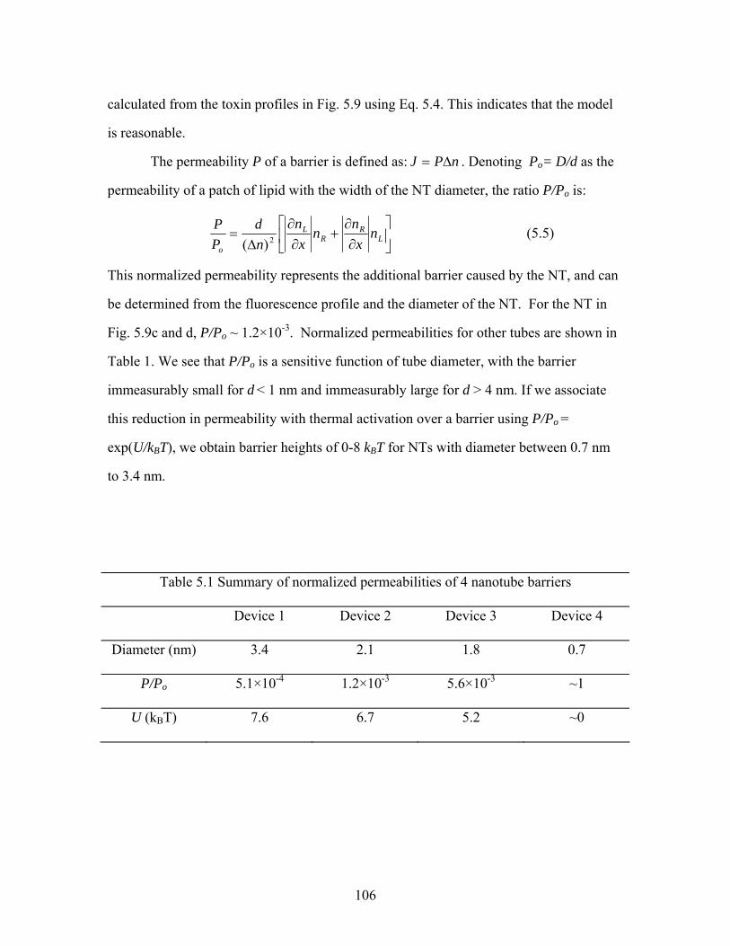
106
calculated from the toxin profiles in Fig. 5.9 using Eq. 5.4. This indicates that the model
is reasonable.
The permeability P of a barrier is defined as: nPJ ∆= . Denoting Po= D/d as the
permeability of a patch of lipid with the width of the NT diameter, the ratio P/Po is:
⎥⎦
⎤⎢⎣
⎡∂
∂+
∂∂
∆= L
RR
L
o
nx
nnx
nnd
PP
2)( (5.5)
This normalized permeability represents the additional barrier caused by the NT, and can
be determined from the fluorescence profile and the diameter of the NT. For the NT in
Fig. 5.9c and d, P/Po ~ 1.2×10⁻³. Normalized permeabilities for other tubes are shown in
Table 1. We see that P/Po is a sensitive function of tube diameter, with the barrier
immeasurably small for d < 1 nm and immeasurably large for d > 4 nm. If we associate
this reduction in permeability with thermal activation over a barrier using P/Po =
exp(U/kBT), we obtain barrier heights of 0-8 kBT for NTs with diameter between 0.7 nm
to 3.4 nm.
Table 5.1 Summary of normalized permeabilities of 4 nanotube barriers
Device 1 Device 2 Device 3 Device 4
Diameter (nm) 3.4 2.1 1.8 0.7
P/Po 5.1×10⁻⁴ 1.2×10⁻³ 5.6×10⁻³ ~1
U (kBT) 7.6 6.7 5.2 ~0

107
The suppression of lateral transport of membrane proteins by the nanotubes is
reminiscent of similar behavior in cellular membranes where proteins are typically
confined in microdomains. A hypothesis consistent with the appearance of functional
microdomains is diffusion hindrance by the underlying protein scaffold. Cells have a
cortex (Pesen and Hoh 2005), a network of linear proteins (e.g. actin or spectrin (Bonetta
2005)) located adjacent to the plasma membrane. This is shown in a schematic of cell
membranes in Fig. 5.10, which is more complicated and closer to reality than the Mosaic
Model mentioned in Section 4.1. Some studies indicate the cortex provides structural
support to the membrane and is involved in the dynamic remodeling of the plasma
membrane (Tank et al. 1982; Kusumi et al. 2005).
Currently the correlation between membrane functionalities with their complex
diffusion properties is under investigation. However, people previously have not been
able to make diffusion barriers in SLBs systems. A mesh of nanotubes (Fig. A.3) can be
used as a platform to probe this interesting phenomenon. In principle, the magnitude of
nanotube barriers can be tuned with electrical potential since the proteins are charged.
Initial trials did not reveal this effect. If that turns out to be feasible, nanotube meshes can
match the cell’s ability to dynamically change protein distributions.
Figure 5.10: A schematic model of cell membrane. This is closer to reality than Fig. 4.1.

108
5.5 Electrical detection of protein binding
With the physical properties of SLB/SWNT hybrid established, we used the
transistor properties of the NT to detect the specific binding of proteins to membrane-
imbedded targets. The streptavidin/biotin system (Chaiet and Wolf 1964) was chosen for
its high binding affinity. A mixed lipid composition, 93.9:4:2:0.1 DOPC:1,2-Dioleoyl-3-
Trimethylammonium-Propane (DOTAP):1,2-Dioleoyl-sn-Glycero-3-
Phosphoethanolamine-N-(Cap Biotinyl):DHPE-LR, was used to form SLBs
functionalized with biotin, as shown in the upper right inset to Fig. 5.11. All lipids were
from Avanti Polar Lipids. To minimize ionic screening, 1 µM PBS buffer with 10 µM
NaCl was used.
Note the positive charge on DOTAP and negative charge on the biotinylated lipid.
The purpose of DOTAP is to facilitate the SLB formations. When only biotinylated lipids
are mixed into DOPC vesicles, they do not form SLBs in the low ionic strength buffer. It
is speculated that the electrostatic repulsion between biotionylated lipids and silicon
oxide surfaces, which have negative surface charges in this condition, prevents vesicle
fusions on the substrates. The addition of DOTAP solved this problem.
To isolate the electrodes from the electrolyte, the device was covered with a 30
nm thick Al2O3 layer except in the regions between the source and drain electrodes
containing the nanotubes, as shown in the lower left inset. When the Al2O3 layer is used
in combination with microfluidic channels, the leakage current between the electrodes
and the water solution is minimized. To reduce noise, a 10 mV AC source-drain bias at
155 Hz was applied across the SWNT FETs and the conductance G was measured with a
lock-in amplifier. A gold electrode immersed in the buffer solution controlled the
potential Ve of the solution (Rosenblatt et al. 2002; Larrimore et al. 2006). All
measurements were done in the same buffer after unfused vesicles and unbound proteins
had been flushed out of the channel. SLBs formed only in regions not covered with Al2O3.

109
Fluorescence microscopy revealed that the SLBs formed were uniform and laterally
mobile, and that the streptavidin/ biotin binding was stable even after washing.
Figure 5.11 shows how the conduction of SWNT FETs was affected by SLBs
formation and streptavidin binding to the biotins imbedded in the SLBs. The solid black
curve in the main panel of Fig. 5.11 shows G vs. Ve before the lipids were added, while
the red dashed curve was taken after the formation of SLB. The positively-charged SLB
significantly shifted the threshold voltage Vt of the NT FET. However, this cannot be
attributed entirely to charges on the SLBs. As shown in Fig. 5.12, similar shifts are
observed when neutral DOPC lipids are formed on SWNT-FETs in 1X PBS buffer. The
average shift is 240 ≤ 70 mV. The threshold voltage shifts backwards when the SLB is
removed with detergent. The mechanism of this phenomenon is under investigation. It is
suspected to be related to the intrinsic dipole of DOPC (Fig. 4.3). But the silicon oxide
surface and the water cushion layer between the SLBs and the substrate can also be the
cause. The magnitude of the shift was larger with this positively charged lipid mixture in
low ionic strength buffer in Fig. 5.11.
After the formation of SLBs with embedded biotins, the device was then
incubated with 5µM streptavidin for 10 minutes and rinsed. The bound streptavidins
shifted Vt back toward positive voltages, as shown by the green dotted curve in Fig. 5.11.
No shift was observed in control experiments where proteins that do not bind to biotin
were added (e.g. tetanus toxin), demonstrating the specificity of the detection.

110
Figure 5.11: Detection of biotin-streptavidin binding with SWNT FETs. Conductance
versus electrolyte potential of a small-bandgap NT FET before (solid black) and after
(dashed red) biotinylated SLB was formed on the surface. The dotted green curve was
taken after streptavidins bound to membrane-imbedded biotins. Lower inset: Optical
micrograph of devices used for sensing. The pink rectangular region between two yellow
electrodes is the only opening in the Al2O3 insulation layer. Upper inset: Schematic of a
carbon nanotube under biotin-functionalized lipid bilayer.

111
Figure 5.12: Detection of DOPC SLB formation with SWNT FETs. Current under
constant 10 mV bias versus time for a SWNT FET during formation of a DOPC SLB in
1X PBS buffer. The drop in conductance happened when vesicles fused on the SWNT.
Lower inset: Current versus Ve for a semiconducting SWNT FET before (black solid
curve) and after (red dotted curve) SLB was formed on top. Upper inset: Histogram of
the threshold voltage shifts induced by DOPC SLB formation in 1X PBS buffer.

112
For the six devices studied, the shift of threshold voltage ∆Ve caused by
streptavidin binding was ∆Ve = 80 ± 20 mV. Using the model in reference (Artyukhin et
al. 2006) that relates voltage shift induced by a layer of charge to its charge density:
dweV λεεσ /2 0∆= , where wε is the dielectric constant of water and dλ is the Debye
length, we estimate that the observed ∆Ve corresponds to an additional charge layer with
σ = -7×10³ e/µm2. The sign of σ agrees with streptavidins being negatively charged at the
buffer pH and the charge density is comparable to the biotin density in the SLB of 3×10⁴
/µm2. The correlation can also be viewed from a surface potential point of view. Refer to
Appendix D for discussions.
The system studied is only one example of specific binding detection, any other
charged protein that binds to a target located within the SLB should cause a similar effect
on the SWNT FETs. The bilayers can be readily functionalized with many molecules. It
is feasible to use the SLB/nanotube hybrids to study other binding systems. Another
advantage of the structure is it eliminates the influence of chemically-active silicon oxide
surface, whose surface chemistry and charge density are easily modifiable to complicate
experimental observations. The lipid surface is relatively inert compared to silicon oxide,
and helps to isolate the events of interest.
In conclusion, we have used electrical and fluorescence measurements to probe
supported lipid bilayers formed over carbon nanotube transistors. We show that the lipid
molecules in a SLB can diffuse freely across nanotubes while ganglioside-bound toxins
see a NT-diameter-dependent diffusion barrier. We further demonstrate electrical
detection of protein binding on the lipid bilayers with NT transistors. This new lipid/NT
model system has many potential applications to the study of both electrical and
mechanical perturbations at cell membranes. This system can also serve as a generic
platform for bringing mobile lipid-bound molecules and NTs in close proximity for
studies of the physical, electrical, and optical interaction of single molecules with NTs.

113
CHAPTER 6
CONCLUSIONS
6.1 Summary
We have studied electron transport in carbon nanotubes in the electron-phonon
scattering limited regime and found out the performance limits of nanotube transistors as
well as the dependence of their resistance and mobility on tube diameter and temperature.
We have also integrated nanotubes with supported lipid bilayers (SLBs) and used this
structure to detect protein binding events on the bilayers.
To learn the intrinsic electrical properties of nanotubes, we performed systematic
studies of nanotube transistors using moderately long and high quality nanotube samples
in Chapter 3. Their electrical conductance and mobility were measured at various
temperatures and correlated to their diameters. It was found out that, after the influence of
the contact resistance was eliminated, the conductance grows linearly with tube diameter
while mobility grows quadratically with tube diameter. They both scale inversely with
temperature, indicating the important role of phonons. A theory model was established,
based on electron-phonon scatterings, to explain how the electrical transport is modulated
by gating and temperature. It predicts the same scaling behaviors as observed in the
experiments and agrees favorably with the measured conductance and mobility values. In
conclusion, this study shows the electron-phonon scattering is the dominating source of
resistance in long nanotubes, and gives performance limits of nanotube transistors
working in this regime.
We integrated carbon nanotubes with supported lipid bilayers in Chapter 5.
Experiments were carried out to confirm the quality of SLBs by measuring the lipid
diffusion coefficients. Lipid diffusions near nanotubes were also tested to show that lipids
can diffuse over the nanotubes without much hindrance and the bilayer is continuous over

114
the nanotubes. However, nanotubes act as barriers for a protein bound to a membrane-
embedded receptor. This hybrid structure was used to detect biotin-streptavidin binding
events on the bilayer in low ionic buffer. The observed signal can be related to the protein
charges. In conclusion, besides being sensitive electrical detectors, the SLB/nanotube
hybrids can be used to probe the correlation between protein diffusion properties and
their functions.
6.2 Future directions
We have presented the current status of our research on lipid bilayers with
nanotubes in Chapter 5. However, it should not be view as an end, but rather as just a
beginning. We have not yet really touched the biological function of membrane proteins,
which are important cell constituents. Some of them control the transport of various
molecules/signals (Doyle et al. 1998) into and out cells while some others are responsible
for generating energy inside cells (Salafsky et al. 1996). A few examples of the
properties that could be studied with lipid bilayer/nanotube hybrids are: diffusion
coefficients of membrane proteins, transport properties of ion channel
proteins/photosynthetic centers, association/dissociation rates of reversible
protein/receptor bindings, and charge detection of single proteins. The high sensitivity of
nanotube FETs combined with micro-fabricated structures allows most of the studies to
be done at single protein level with high speed to reveal properties that are otherwise
concealed due to averaging. Another direction of the proposed future research will be to
integrate carbon nanotubes with real cells. The conduction channel of the nanotube FET
can be placed either close to a cell membrane or even inside the cell and used as a sensor
or electrical probe.
Applying nanoelectronic science and technology into biology is a new field and
has a promising future. The proposed projects are examples of using nanoscale structures

115
as electronic interfaces to study biology at single-molecule level in an unconventional
way.
Probing membrane protein dynamics
Although we have been able to specifically detect protein bindings to membrane-
embedded receptors in Section 5.5, more information can be obtained from this
experiment. The induced threshold voltage shift fluctuates when proteins diffuse around
nanotubes. In principle one could study the noise spectrum of lipid bilayer/nanotube FET
hybrids, distinguish the part of noise that is induced by membrane proteins in the lipid
bilayers and extract their properties such as diffusion coefficients and charge densities.
The experimental scheme is inspired by optical FCS, mentioned in Section 5.2. But in
this proposed experiment, the current change induced by the presence of membrane
proteins plays the role of fluorescence intensity in FCS. The merits of this experiment
over FCS are it does not require labeling molecules with fluorophores and offers higher
spatial resolution.
In this experiment, neutral SLBs with membrane proteins would be first formed
on top of nanotubes in the same geometry as Fig. 5.3 shows, and the noise spectrum or
current fluctuations of nanotube FETs under constant bias should be recorded before and
after introducing molecules to bind with the membrane proteins. With careful modeling
and calibration using proteins of known diffusion coefficients and charge densities, a
correct fitting to the data should provide these two parameters of other proteins.
The characteristic time scale in this experiment is set by the Debye screening
length ld of the buffer solution, and the diffusion coefficient (D) of membrane proteins.
To minimize charge screening, the experiment should be carried out in buffers with ld
~100 nm. The typical value of D is around 1 mm2/s, and the time scale for membrane
proteins to diffuse through the nanotube FET detection area is about 10-3 s. This is well
116
within the ability of most spectrum analyzers or current pre-amplifiers. One benefit of
looking at these high-frequency signals is that nanotube becomes a quieter sensor at
higher frequency because 1/f noise is the dominating noise source in SWNT-FETs
(Collins et al. 2000).
Study of protein binding dynamics at single molecule level
The experiment proposed in last part deals with the statistical behavior of multiple
proteins. Another ambitious experiment scheme is to reach higher charge sensitivity by
reducing the length of nanotube conduction channel. In the experiment illustrated in Fig.
5.11, the detection limit is about 2 mV in gate voltage at 1 KHz bandwidth. It means that
when the gate voltage is shifted by 2 mV, the induced current change can barely stand out
of the noise. Using the known capacitance of nanotube in solution (Rosenblatt et al. 2002)
C = 4µ 10-10 F/m, this corresponds to bringing 5|e| into a 1 mm long nanotube FET. If the
conduction channel is further reduced to 100 nm, this system can reach single charge
sensitivity regime. Then it is possible to see the on-off signatures of a single reversible
binding event or the lateral diffusion of a single protein.
To study the association/dissociation dynamics, it is better to have static proteins
near nanotube FETs, since the membrane proteins are diffusing in the bilayer all the time.
This part of study may be done with chemically functionalized nanotubes, to which
proteins are directly attached (Besteman et al. 2003). This opens up possibility of
studying even more types of molecules besides membrane proteins.
Probing the transport properties of transmembrane proteins
One advantage of the lipid bilayer/nanotube hybrid structure is that there is a
continuous membrane separating the bulk solution from the water layer underneath the
SLB, where nanotube sits. Therefore a new kind of interesting experiment can be based

117
on using nanotubes as electrodes to probe the potential difference between the two water
regions on each side of the membrane.
Membrane proteins can produce an ion concentration difference across a
membrane, which generates an electrical potential according to Nernst equation DE =
ln(C2/C1) µ kBT/ne, where C2 and C1 are the ion concentration inside and outside the
membrane, and kBT/ne is about 59 mV at room temperature for n = 1. Two examples of
proteins that can generate cross-membrane potentials are: (1) Bacteriorhodopsin, which
absorbs light and uses this energy to pump protons across the membrane (Khorana 1988),
and (2) potassium ion channels, which selectively transport potassium ions across the
membranes while blocking other ions (Doyle et al. 1998).
In this experiment, the lipid bilayer/nanotube hybrid structure should be slightly
modified to probe this membrane potential. As shown in Fig. 6.1, the nanotube chip
surface would be covered with dielectric layer except the regions around nanotube
conduction channels. A patch of SLB would form at these openings where the nanotubes
sit. Effectively, the nanotubes are contained inside a tiny aqueous chamber. Because
lipid membranes have extremely low permeability to charged ions, the only pathway for
ions to exchange between this chamber and the bulk solution would be through the
membrane proteins.
Ion transport through the membrane proteins would be triggered by external
stimuli. In the case of Bacteriorhodopsin, light can be shone onto the structure. In the
case of an ion channel, the bulk solution could be flushed with a buffer of different
concentrations or ions. The potential associated with these events would be monitored
using nanotubes as electrostatic potential sensors (Larrimore et al. 2006).

118
Figure 6.1: Schematic of the proposed structure to use nanotube as cross-membrane
potential sensor. Nanotube is sealed by a patch of membrane and the surrounding
dielectric (shown as rectangles in granite) layer that defines the well. Membrane protein
bridges the two water regions on either side of the membrane and selectively allows ions
to pass through.
Some membrane proteins lose their function inside SLBs because part of the
protein protrudes out and denatures on the substrate surface as mentioned in Section 4.1.
In that case, lipids with very large head groups, such as polyethylene glycol as a spacer in
the head group, can be used to increase the spacing between SLBs and substrates to a few
nanometers. Another solution is to lay a polymer cushion layer under SLBs (Sackmann
1996).
One needs to get a sense of how small the chambers around nanotubes are.
Regions with ~10 mm2 cross section can be easily fabricated with photolithography, and
ones with ~0.1 mm2 cross section can be made with electron beam lithography. The
height of these chambers is the thickness of the water cushion layer between SLBs and
Figure 3. Schematic of proposed structure to use nanotube as cross-membrane potential sensor. Nanotube is sealed under a patch of membrane and the surrounding dielectric layer. Ions can only exchange between the bulk solution and the water cushion layer through membrane proteins.

119
substrates, which can be as small as 1-2 nm. The volumes of these chambers are therefore
around 10 aL to 0.1 aL.
With such a small volume underneath a SLB, even a single protein can generate a
detectable cross-membrane potential on a short time scale. Let us consider potassium ion
channels as an example. Suppose the chamber volume is 10 aL and the initial buffer is
100 mM potassium chloride. When the bulk solution is replaced with 1mM potassium
chloride and the potassium channel is opened, a single protein can decrease the
concentration of potassium ions underneath the membrane down to 1mM within 6 ms
(using the reported transport rate of ~108 ions/sec (Saparov and Pohl 2004).) The
concentration difference of Cl- ions across the membrane will produce a potential
difference of about 120mV, which can be easily detected by nanotube FETs. However, it
would be interesting to see how the transport rate slows down with increasing cross-
membrane potential and at what potential the ion transport stops. This technique allows
study of the functioning of single membrane protein in real time.
If the chamber volume is reduced to 0.1 aL and the potassium ion concentration is
10 mM to start with, the outflow of a few hundred potassium ions from the chamber can
be detected. This is a sensitivity no other technique can reach. Another advantage of this
powerful tool is that multiple studies can be done in parallel on a single chip.
Nanotube/SLB hybrids can become an important new platform for studying the function
of single membrane proteins.
Integrating nanotube FETs with cells
Naturally, the next stage of this series of experiments is to study real cells. This
can be done in two schemes: (1) place nanotubes directly against the external side of the
cell membrane, or (2) place them inside cells. These experiments may lead to the

120
invention of electrical sensors that can directly monitor single cell activities and measure
properties inside cells that cannot be done with current methods.
In the first scheme, the patch of SLB in Fig. 6.1 can be replaced with a real cell
membrane. Recently Prof. Lieber’s group at Harvard University demonstrated that
neuron activities can be detected with nanowire array (Patolsky et al. 2006) in a similar
fashion. Since nanotubes have higher mobility and transconductance (Rosenblatt et al.
2002; Zhou et al. 2005), integrating cell membranes with nanotube FETs will offer higher
sensitivity compared to nanowires. The well formed by dielectric layers around
nanotubes in the proposed structure in Fig. 6.1 not only helps to minimize the sensing
region to a small area, but also helps to confine the product molecules of cell activities
around nanotubes. It will further improve the signal strength.
In the second scheme, a special property of SWNTs will be applied: their
ultimately-small sizes. SWNT diameters are comparable to that of a DNA molecule.
Therefore it may be possible to put the conduction channels of nanotube FETs inside
cells without drastically disturbing them. A structure is proposed as shown in Fig. 6.2.
The substrate underneath nanotubes is etched away so that nanotubes are suspended in
solution. A cell will be brought in with a micromanipulator and put on top of a suspended
nanotube FET. The suspended part of nanotube has a chance of penetrating the cell
membrane and entering into the cell body. It will be interesting to see how this is going to
affect cells and if cell skeletons and membrane cortexes will stop this intrusion.

121
Figure 6.2: Left, schematic of a nanotube (green cylinder) suspended over a trench.
Right, when a cell (magenta sphere) is placed on top of a suspended nanotube, the
nanotube may be able to penetrate inside the cell.
If suspended part of nanotube FETs do indeed go inside cells, it could act as a
detector to sense the ongoing electrical activities inside the cell or an electrical probe to
control those processes! There are many fascinating experiments to perform. For example,
carbon nanotubes have been functionalized to detect glucose concentration in solution
(Sotiropoulou and Chaniotakis 2003). Nanotubes can be modified with the same
chemistry and do sensing inside cells with this method. Besides molecule sensing,
nanotubes can also serve as electrodes to probe the electrical potential inside cells, or to
stimulate cells with electrical pulses. A wilder idea is to break nanotubes inside cells by
running relatively high current (~20 mA) through them, which turns a single nanotube
into two adjacent electrodes. They could be used as dielectrophoresis tweezers (Zheng et
al. 2004) to manipulate molecules. Currently micropipette can be inserted into cells. This
proposed nanotube probe, however, is less intrusive due to its much smaller size, and has
higher spatial resolutions to map out different regions of cell bodies.
In conclusion, carbon nanotube transistors are novel systems that offer promises
in diverse areas ranging from real-time observation of protein dynamics to the study of

122
cell activities. They can solve fundamental scientific questions as well as generating new
tools for biophysics. Using nanotubes to electronically ‘see’ single molecules has the
potential for the same kind of scientific impact as single molecule fluorescence
techniques have demonstrated. However the ideas offered here are not guaranteed to
work, some of which may not be even theoretically correct. They are provided to
stimulate people’s wildest imaginations to discover the potential of the new nanometer
tools.

123
APPENDIX A
NANOTUBE GROWTH
The Japanese has a proverb: those who control materials will control technologies.
This is certainly true in some sense. Material growers are highly appreciated in Japan. It
has enabled them to have some of the best material samples in the world. Carbon
nanotube was discovered in Japan in 1991 (Iijima 1991), which may or may not have
been accidental.
Although our lab is in Physics, but the current situation forces us to grow
nanotubes ourselves. Therefore it is important for Physics students to master nanotube
growth. I recommend new students spend their first few weeks in the furnace room. This
is the hardest part of making devices. Compared to the cleanroom part, which is very
standardized and highly repeatable, nanotube growth still remains in the dark magic
phase and one needs to get some kind of feeling. When the device fabrication fails, more
than often it is due to something in the furnace. To emphasize the importance of materials,
a story about graphene must be told. Many years ago our beloved adviser, if not the first
person, had foreseen the unique physics and potential impacts in graphene. But no one
could make a high quality single layer graphene until a group in University of
Manchester was lucky enough to find an effective way to do so (Novoselov et al. 2004).
It is indeed a gold mine.
The situation in the case of nanotubes is better. It is very easy to grow nanotubes
using chemical vapor deposition (CVD) in our lab. But it is somewhat hard to get exactly
the kind of nanotubes needed. The properties need to be controlled include tube diameter,
length, orientation, yield and cleanness. Chirality control would be great, but it is
impossible as of today. Here, I will share some experience and techniques from me and

124
other people in the lab. Not everything is guaranteed to be correct. Possible
improvements that have been demonstrated by other groups will also be presented.
Diameter control
It can be seen in almost every chapter of the thesis that diameter is one the most
important parameters of nanotubes. The bandgap of a semiconducting nanotube is
inversely proportional to tube diameter and the mean free path goes linearly proportional
to diameter (Chapter 2, 3). It is widely accepted that, in CVD growth, the tube diameter is
controlled by the size of the catalyst nanoparticles (Cheung et al. 2002). Personally, I
think it is not entirely true in at least one respect: it is hard to imagine growing large
nanotubes from much smaller particles; but it is possible to grow tubes smaller than the
particle size, especially if the catalyst particles are not in liquid phase (Kodambaka et al.
2007).
Since there is typically a broad diameter distribution with any kind of growth
recipes, we can select the nanotubes with the targeted diameters. The standard recipe,
900 ±C Methane growth, normally gives large diameter tubes (Kong et al. 1998). In their
original paper, Dai group claims that the tubes are between 1-3 nm. However, the tube
diameters were measured using AFM at scan range of 10 µm. This dramatically
underestimated the tube diameters. The good thing is that the authors have done extensive
TEM studies to show their fat tubes are still single-walled. The other recipes, using very
thin evaporated iron film as catalyst or soaking chips in iron nitride/methanol solution
and growing at 700±C with Ethylene, tend to give thinner tubes in my experience.
If one wants to do better than that, efforts need to be put into making near
identical catalyst particles and preventing them from aggregation at high temperature. A
few recipes with better diameter control involve using Ferritin protein (whose iron
content can be controlled) (Li et al. 2001), block copolymers (size of iron containing

125
segment can be controlled as well) (Lu et al. 2005) and identical metal containing
nanoclusters (An et al. 2002). But complicated catalyst preparations go beyond the ability
of Physics students. Collaborations may be needed.
Long and aligned nanotubes
Having longer tubes is never a disadvantage. They enable ones to study the
intrinsic properties of nanotubes in electrical transport and optical applications. The first
method that can get individual nanotube longer than one centimeter was discovered by
Jie Liu’s group at Duke University (Huang et al. 2003). The key to this recipe is to get
catalyst particles off the substrate, by the turbulence as a result of fast heating, so that the
growth is happening in the gas (Huang et al. 2004). Liu argues that the strong Van der
Waals interactions between substrates and tubes/catalyst make them difficult to slide on
the surface, and stop the growth prematurely.
We were lucky to learn their fast heating technique. Although our tubes are not as
long as theirs and the yield is not very high, but it still can help us in many cases. The less
satisfactory results in our lab may be due to the different carboneous gas we use
(Methan/Ethylene) as compared to theirs (Carbon monoxide).
There are other recipes to grow long tubes without the fast heating step. Liu group
also used an alcohol CVD to grow centimeter long tubes without any special measures to
lift up the catalyst (Zheng et al. 2004). But this does not rule out the possibility that the
tubes are flying in gas during growth. Another amazing result from a UIUC group,
however, shows that their long tubes are actually grown on the substrates (Kocabas et al.
2006). Figure A.2 is taken from their publication. The substrate is [2,1,10] single-crystal
quartz wafer. The nanotubes have a preferred orientation and can grow more than 100 µm.
Similar effects have been seen on more expensive Sapphire substrates as well (Han et al.
2005). Since people in our groups are growing tubes on transparent quartz substrates to

126
either eliminate the backgate or to allow better optical imaging, it should be natural to try
these single-crystal quartz substrates with special cuts, if they are not too expensive.
Figure A.1: Two long (~100 µm) nanotubes grown with the Duke recipe in our group.
Figure A.2: Long and highly aligned nanotubes grown on quartz substrates (Kocabas et
al. 2006).
5 µm

127
Yield
Normally the yield is not a problem in our lab. One can adjust catalyst
concentration, catalyst pad size and other parameters to control the yield to a preferred
level. There are two cases where yield needs to be significantly increased. First in some
experiments, it would be great to have really densely packed nanotube mashes. One
example is Jose and I wanted to suspend lipid bilayers with nanotube mashes as support.
Second, the fast-heating long tube growth recipe generally gives sparse nanotubes. One
problem with that recipe is the nanoparticle catalyst easily gets off the wafer during the
lift-off process that is used to define catalyst pads. In both cases, a better lift-off process
can help.
Currently catalyst pads are defined using photoresist or electron beam resist. The
lift off is done in a solvent, either organic or water, to dissolve the resist, during which
catalyst can get off the substrates. A dry lift process can solve this issue. The key is a
polymer called parylene (Zhang et al. 2003; Moran-Mirabal et al. 2005) . A few
properties make it an ideal material. First, a thin layer (~ µm) can be deposited on
substrates from gas phase. CNF recently bought a machine to do that. Second, parylene
does not dissolve in common solvents, and is compatible with photo lithography
processing. A layer of normal photoresist can be spun on top of parylene film to define
micrometer size features, which can then be transferred into parylene layer by oxygen
plasma etching. Third, the parylene layer, although extremely thin, can be mechanically
peeled off from the substrates using tweezers.
Figure A.3 shows a SEM image of nanotube meshes made for the lipid bilayer
suspension purpose. The rectangular, where nanotubes are densely packed, was initially
defined using parylene film. Nanoparticle catalyst solution was dried on the surface,
followed by peeling off the parylene film. The end result is a nice nanotube mesh without
too much catalyst residue.

128
Figure A.3: A dense mesh of nanotubes grown in a region defined by parylene.
I have not tried to increase the fast-heating growth yield with this trick yet. The
parylene technique should also be useful for other purposes where the dry lift-off is
desired.
Vertical nanotube forest
Another different type of CVD nanotubes is called vertical nanotube forest.
Basically, when the nanotubes are densely grown (one per 20 nm x 20 nm), the Van deer
Waals interaction will facilitate them to stand up and form a forest-like structure.
Typically people in our lab are not interested in this type of nanotubes since we
study individual ones. However this could be useful for our collaborators and we can
exchange the nanotube forest for their help. The key to nanotube forest is density. First,
the catalyst particles need to be densely packed. Second, most of the nanoparticles need

129
Figure A.4: Nanotube mesh grown without water vapor in the CVD chamber.
Figure A.5: Aligned nanotube forest grown with water vapor in the CVD chamber.

130
to be active during growth. These two conditions would prevent nanotubes from falling
onto substrates during growth.
A thin layer of iron is typically used as catalyst particle precursor. The iron film
breaks into individual particles at elevated temperature. Even a 0.5 nm iron films (this
value should be consider as nominal) can lead to large particles and thus multi-walled
nanotubes. Many groups use underlayers such as alumina oxide or molybdenum beneath
the iron layer. It is not necessary. The key to make catalyst active and remain active for a
long time is introducing small amount of water vapor into CVD chambers (Hata et al.
2004). Figure A.4 is a SEM of nanotubes grown using thin film iron as catalyst. The
growth condition is tuned to extremely high yield, but no water vapor is added. The
nanotube density is high, but it is not high enough for nanotubes to stand up. The vertical
nanotube forest shown in Fig. A.5 is grown under the same condition except a small
amount of water vapor is added. It seems to indicate, besides etching way amorphous
carbon coating on catalyst particles to prevent them from being poisoned, water also
helps to make every catalyst particle work from the very beginning. The water content is
not carefully controlled in this case. Mine record is 5 mm tall forests. And the world
record is a few centimeters.
In conclusion, there are many tricks to grow nanotube for one’s special needs. We
should not be constrained by the kind of tubes we can make. Better tubes can lead to new
functionality.

131
APPENDIX B
VALIDATION OF THE THEORY MODEL IN CHAPTER 3
When the experimental data and theory calculations on electron-phonon limited
transport are presented in Chapter 3, it seems the theory in Sections 3.2-3.4 is able to
explain most of the experimental observations. But it does not include many subtleties.
Here are two examples of some major concerns: 1. Does conduction depend upon the
chirality of nanotubes? 2. What if more than one subband participates in transport?
These questions will be addressed in this appendix.
Chirality
Up to today, people do not have the ability to control growth conditions to get
tubes with specific chirality. In many cases, it is almost impossible to determine the
chirality of a nanotube sample. It can be done with STM or a few optical spectroscopy
techniques as mentioned in Chapter 1. But the processes are difficult to carry out on the
device geometries that are typically used to study transports. In our experiments, the
chirality of a nanotube device is not known. And there is no reason not to believe that the
chiralities of an ensemble of nanotube devices are widely distributed over all possible
values.
Not surprisingly, in many cases chirality comes into the horizon. In Minot’s study
of nanotube band structure modulations from mechanical deformations (Minot et al.
2003), the degree to which the band structure is modified strongly depends on the
nanotube chirality. Similarly, it turns out the electron-phonon coupling is chirality-
dependent. But as the following discussion shows, this dependence in semiconducting
nanotubes is relatively weak.

132
In Section 3.3, the deformation potential D is assumed to be a constant value
disregarding nanotube chirality. Let’s see if that is valid. T. Ando (Suzuura and Ando
2002; Ando 2005) theoretically studied the electron couplings to different modes of
phonons and gave the interaction Hamiltonian as
⎟⎟⎠
⎞⎜⎜⎝
⎛∗
12
21
VV
VV (B.1)
where V1 = g1 (∑ux/∑x+∑uy/∑y) and V2 = g2 exp(3ih)(∑ux/∑x-∑uy/∑y+∑ux/∑y+i∑uy/∑x) with
u being the displacement and h as the chiral angle. The x direction is along the
circumference and the y direction is along tube axis. The coupling constant g1 and g2 is
estimated to be on the order of ~30 eV and ~2 eV. The off-diagonal terms are much
smaller in magnitude.
The normalized electron wavefunction in nanotubes can be written as
( ) [ ]ikyxnikFdL
F vsnk += )(exp1π
r (B.2)
( )⎟⎟⎠
⎞⎜⎜⎝
⎛=
1,
21 knsb
F vsnk (B.3)
( ) ( )( ) 22
,knk
iknkknb
v
vv
+
−= . (B.4)
Here s equals +1 for the conduction band and -1 for the valence band. n is the subband
index and kv(n) = 2(n-v/3) /d is the wavevectors long tube circumference. In metallic
tubes, kv(n) =0 for the first subband. In semiconducting tubes, kv(n) is the bandgap
divided by Fvh2 .
The wavefunction looks complicated, but it is actually simple. It is a plane Bloch
wave. The variable bv(n,k) gives the phase difference between the electron wavefunctions
at the two carbon atoms in a unit cell. For the first subband in a metallic tube, kv(n) =0,
the wave function is
( ) [ ] ( )⎟⎟⎠
⎞⎜⎜⎝
⎛−=
1/
21exp1 kkis
ikydL
Fπ
r . (B.5)
Then the matrix element of the phonon-electron scattering is proportional to

133
212
21 Re1
1
Viis
VVVVis
−=⎟⎟⎠
⎞⎜⎜⎝
⎛−⎟⎟⎠
⎞⎜⎜⎝
⎛⎟⎟⎠
⎞⎜⎜⎝
⎛∗
+
(B.6)
This shows that the diagonal terms do not induce scattering in metallic tubes.
Only the much smaller off-diagonal terms generate resistance. This effect is due to the
Berry phase, or pseudospin, that the electrons carry in nanotubes (Ando et al. 1998;
McEuen et al. 1999) . In short, the wavefunctions of the left moving and right moving
electrons are made of bonding orbital and anti-bonding orbital respectively. Because the
long wavelength acoustic phonons cannot change the electronic states at the atomic scale,
the transition between left and right moving electrons cannot be induced by them.
The off-diagonal term
⎥⎥⎦
⎤
⎢⎢⎣
⎡⎟⎟⎠
⎞⎜⎜⎝
⎛∂
∂+
∂∂
−⎟⎟⎠
⎞⎜⎜⎝
⎛∂
∂−
∂∂
= ηη 3sin3cosRe 22 xu
yu
yu
xu
gV yxyx (B.7)
depends on chiral angle h. Indeed the relaxation time of a metallic nanotube is
ητ
ηττη
3cos13sin11 22
ZA
+= , (B.8)
where tA and tZ are the relaxation time of an armchair and a metallic zigzag tube of the
same diameter.
T. Ando (Suzuura and Ando 2002) pointed out that tA and tZ are equal when
temperature is much higher than the radial breathing mode (RBM)
temperature BBB kT /ωh= . In that case, the conductance of a metallic tube does not
depend on chiral angle. Figure B.1 shows calculated resistivity as a function of
temperature for three nanotubes of different chirality but the same diameter (Suzuura and
Ando 2002). At high temperature, the three curves are on top of each other. That means
near room temperature, the resistivity of nanotubes is chirality-independent.
In Fig. B.1, the overall decrease of the resistivity with lower temperature is caused
by acoustic phonon occupation effect. For low energy long wavelength acoustic phonons,
the phonon population is proportional to temperature. But the radial breathing mode
phonons, which contribute to scattering in all tubes except armchair tubes, disappear

134
Figure B.1: Calculated resistivity as a function of temperature for three nanotubes with
different chiralities (Suzuura and Ando 2002).
rapidly at lower temperature. This is because the dispersion of RBM phonons is not linear.
As Fig. B.1 shows, zigzag tubes become slightly better conductors at lower temperature.
The difference between the resistivity of armchair tubes and zigzag tubes could reach a
factor of two at very low temperature.
For semiconducting nanotubes, the situation is quite different. The matrix element
is calculated as ( ) ( )[ ]
( )( )[ ]
( )222122
12
21 Re,,
,, V
knk
iknksV
knkiknknk
knsVV
VVkns
v
v
v
vv
+
−+
+
−=+⎟⎟
⎠
⎞⎜⎜⎝
⎛−
∗. (B.9)
Obviously, the much larger diagonal V1 term dominates at the bottom of the
subbands where k is small. Since V1 is chirality-independent, the matrix element is the
same for all nanotubes in that situation. However, as the subband is filled more and more,
the importance of V1 decreases as the factor ( ) ( ) 22/ knknk vv + goes small with

135
increasing k. That means the chirality dependent off-diagonal term V2 becomes influential
at higher Fermi energies. But as has been shown before, even in metallic tubes, where V2
term is the only mechanism for back scattering, the resistivity does not depend on
chirality at high temperature and only varies by not too much at low temperature. So this
can be considered as second order effect.
In conclusion, one can assume, to a certain extent, the resistivity is the same for
nanotubes of the same diameter independent of their chirality. The maximum field effect
mobility, which is present at intermediate Fermi energy, should depend even less on
chirality.
Subbands
In Chapter 3, all calculations are based on electron transport in the lowest subband.
However the higher subbands can be filled when more and more electrons are put into
nanotubes by electrostatic doping from the nearby gates. It is easy to estimate how
quickly the second subband can be reached, disregarding thermal smearing effects.
Using the simplified band structure in which the energy of the second subband
bottom is Eg,
( ) 222
2 gFg Ekv
E=+⎟⎟
⎠
⎞⎜⎜⎝
⎛h , (B.10)
we can get the wavevector at which the second subband is reached,
dvE
kF
g
32
23
==h
. (B.11)
Assuming the gate capacitance to be 2µ10-11 F/m, the same value as in our FET devices
with 200 nm silicon oxide layer, the second subband is reached at gate voltage
[nm]
V12d
VV tg =− . (B.12)

136
For a 3 nm diameter tube, the second subband is reached when gate voltage is 4 V
above the threshold. In typical measurements, the gate voltage is swept from -10 V to
+10 V. That means there is normally more than one subband filled at high gate voltage.
It is naïve, however, to think that the conductance scales with the number of
populated subbands. Figure B.2 plots calculated conductance as a function of carrier
density for two tubes (Pennington et al. 2007). It shows that, at small gate voltage, the
conductance is slightly lower when multiple subbands are taken into consideration. This
is because inter-subband scatterings reduce the electron relaxation time. The differences
between the cyan curves (single subband) and red/black curves (multiple subbands) in
Fig. B.2 are merely a scaling factor close to 1, demonstrating that it is not a bad
approximation to consider only one subband. On top of that, the current theories on
multiple subbands conductance do not include the contact effects. In principle, because of
the higher energy of the higher subbands, there could be strong Schottky barriers between
the contact metal and the higher subbands, generating large contact resistances and
restricting the conductance through them. Therefore, the higher bands are ignored in
Chapter 3.

137
Figure B.2: Theory predicted conductance through 1 (cyan) and 3 (red/black) subbands
as a function of carrier density/gate voltage (Pennington et al. 2007).
Another noticeable feature in Fig. B. 2 is that when there are more than one
conducting subbands, the conductance is not monotonic when gate voltage is swept. The
differential conductance is negative in certain gate voltage range. This is caused by the
sudden appearance of many states from a higher subband when the Fermi level is moved
close to its bottom. The electrons in the first subband, which initially have high mobility
due to a small DOS at the Fermi level, can be scattered into the states in the higher
subband. The result is, although the number of electrons is increasing, conductance drops.
The tube in Fig 3.2 shows similar behavior at lower temperature and the wiggle happens
around the expected gate value where Fermi level reaches the second subband. However
there is no other evidence to prove this wiggle is caused by the presence of the second

138
subband. Further experiments are needed to definitely establish effects of the second and
higher subbands.
In short, the approximations taken during the calculations in Sections 3.2-3.4 do
not affect the grand picture. They are valid to certain extent as discussed in this appendix.

139
APPENDIX C
FUNCTIONALIZATION OF NANOTUBES WITH DNA
The discussion in Section 5.1 shows why nanotubes are an interesting candidate
as biological sensors. This idea led to the demonstration of nanotube DNA and protein
sensors based on charge sensing in the early stage of this field. Here in this appendix, I
will show the motivation and our initial results on functionalizing nanotubes with DNA,
in route to use them as biosensors. We believe our scheme has a few unique advantages.
Motivation
Here are a few examples of why electronic based DNA and protein sensors are
highly desired. Many diseases are genetic. In other words, they are encoded in a person’s
DNAs from the very moment this person is conceived. One possible way to prevent a
person from genetic disease is to find out the potential threats early and prevent them
long before the person becomes a patient. This requires DNA sequencing or sensing to
detect known segments of DNA sequence responsible for diseases. Currently this process
is slow and requires labeling DNAs with fluorescence tags. The proposed charge-based
sensing can lead to easier, faster and parallel detection for high throughput.
In some sense the protein sensors are even more important. When a disease is
developed in a patient, certain characteristic proteins are produced and can be utilized as
diagnoses indicators. However, the amount of proteins is tiny at the early stages and,
unlike DNA, proteins can not be amplified. This requires protein sensors to have very
high sensitivities. In principle, the proposed nanotube sensors can reach these goals.

140
Specificity is required in electronic biosensors
In order to achieve any practical significance, the electronic biosensors need to
have specificity. But electrostatic interaction, which electronic biosensors base on, is
quite generic. Any charged molecules bound to the nanotubes in these sensors due to
certain reason would perturb the local environment and may generate false signals. The
specificity needs to come from the molecular reorganization developed by Mother Nature
during billions of years of evolution. That requires functionalizing nanotubes with
receptors that allows only the targets to bind to this complex. In the case of DNA, the
receptor attached to nanotubes could be a single strand DNA complementary to the
targeted DNA. For proteins, it can be a compound or another protein acting as the
receptors.
The current status of nanotube biosensors and our proposal
One of the very best properties of nanotubes turns out to be a big obstacle for
functionalization: the fact that a SWNT is just one layer of carbon atoms. Most
functionalizations start with generating functional chemical group on the surface. That
will introduce defects in nanotubes and degrade their electrical properties. The problem
was solved by non-covalent functionalization with a linker molecule designed by Dai
group at Stanford (Chen et al. 2001). The pyrene group on the linker molecule, 1-
pyrenebutanoic acid, succinimidyl ester (Molecular Probes, Inc., USA) shown in the
upper left corner of Fig. C.1, binds to the sidewall of nanotubes due to p-p stacking and
hydrophobic interaction in aqueous solutions. The other side of the link, succinimidyl
ester, readily reacts with primary amine group.

141
Figure C.1: Functionalization of nanotubes with PASE (Chen et al. 2001).
Figure C.2: AFM images taken before (left) and after (right) attaching glucose oxidase
onto nanotubes (Besteman et al. 2003).

142
Since there are primary amine groups in the amino acid residues, e.g. lysine,
proteins are naturally rich in amine groups and can form covalent bonds with the linker
molecules. Several groups have successively absorbed proteins onto nanotubes using this
technique and detected these events as a change in conductance. Dekker group at Delft
(Besteman et al. 2003) attached an enzyme called glucose oxidase to nanotubes, with the
PASE linker, and detected glucose using these complexes. Grüner group at UCLA (Star
et al. 2003) deposited a polymer layer on top of nanotubes and functionalized the
polymer with biotins. The complex was then used to detect streptavidins, which strongly
bind to biotins. The mechanism of the observed electrical signals is disputed over
whether the signal comes from electrostatic gating, charge transfer or change of
capacitance.
The bad thing about the above experiments is that proteins only show up as
globular objects under atomic force microscope (AFM). Therefore it is hard to confirm
these features are indeed proteins in stead of other contaminations. In Fig. C.2, it can be
clearly seen that, after functionalizations, there are many blobs on the substrate far way
from the nanotube. It makes one wonder if the coating on nanotubes is really specific.
Another problem with the current experiment scheme is that it is hard to confirm the
electrical signals, which are merely conduction changes.
Due to the above reasons we started to make our version of DNA sensors using
similar technique but with a few unique advantages. First, we wanted to attach DNAs
longer than 1000 base pairs to nanotubes. These DNAs are so long that they show up in
AFM as linear features. Second, by attaching only the ends of DNAs to nanotubes, it is
possible to drive them close to or away from nanotubes with electrical potentials. By
doing these operations, the electrostatic coupling between nanotubes and DNAs are
modified, which should generate well-controlled signals as a way to confirm the presence
of linear charged molecules. Unfortunately the second part was never tried out due to

143
timing issues. But the functionalization part was successful, and that’s going to be
discussed here.
Fabricating DNAs with modified ends
The first task is to have DNAs with primary amine groups at the ends. Short
strand DNAs that are terminated with all kinds of common chemical groups are
commercially available. But the problem is they are short, typically only up to 50 base
pairs. This is because the yield of making these DNA strands decreases exponentially
with increasing length. In order to have DNAs easily identifiable in AFM, we want to
have DNA longer than 200nm when fully stretched. In other words, the DNAs need to be
more than 600 base pairs long.
This was solved by elongating the short strand DNAs using polymerase chain
reaction (PCR) (Saiki et al. 1985). PCR is typically used to amplify DNAs (to make
multiple copies of a certain part of DNAs). I will try to explain how it works in three
shot paragraphs.
Naturally cells use a protein called DNA polymerase to duplicate DNAs. In PCR,
a number of DNA polymerase proteins are put into the reaction chamber together with
copious amount of nucleotide A,T,C,G. The DNA that is waiting to be amplified is called
the template. The segment of DNA that is going to be copied is determined by two short
strands of DNA called primers, which match the sequence of the ends of the DNA
segment of interest. In short, the reaction chamber is filled with DNA polymerase, the
template, the primers and a supply of A, T, C, G.
PCR is a cyclic process. Each cycle starts with heating the chamber to around 94
degree Celsius for the double strand DNAs to separate and for the polymerase proteins to
terminate their work and get off the template. Then the temperature is lowered to a sweet
spot where the primers can bind to single strand DNA templates. Then temperature is

144
raise to 72 degree Celsius for polymerases to work most efficiently to make copies of the
templates. Polymerase works really fast and can make around 1000 base pairs in one
minute. After a short period of time, determined by the template length, temperature is
raised to 94 degree Celsius and a new cycle starts. The cycle is repeated many times to
get huge numbers of the specific DNA sequence needed. The amount of product grows
exponentially with numbers of cycles.
Figure C.3: Schematic of PCR cycles (users.ugent.be/~avierstr).

145
Since we do not care about the DNA sequence, we randomly chose lambda DNA
as our template. Standardized computer programs helped to choose a segment of lambda
DNA as our target and extracted the sequence of corresponding primers. The primer
selection is crucial to ensure the amplified DNA strands would not form secondary
structures like hairpins with themselves. We chose our final single stranded DNA to be
around either 1000 or 2000 bases long. The primers of the right sequence for our purpose,
with amine-modified ends, were bought from Integrated DNA Technologies (idtdna.com),
and the lambda DNA was bought from New England Biolabs (neb.com). The PCR was
carried out successfully. This was confirmed with gel electrophoresis to measure the
length and purity of our final products.
Putting DNAs onto nanotubes
At this point, DNAs of sufficient length and modified with amine groups at the
ends were made. There were four kinds of them: 1000 base pairs long or 2000 base pairs
long, one end functionalized with amine or both ends. The next step would be to put them
on the sidewalls of nanotubes using the PASE linker.
This can be done in two different methods. One method starts with putting PASE
on nanotubes first. This is done by putting a droplet of PASE in dimethylformamide
(DMF) on a silicon chip with nanotubes on top, and letting them incubate for 10 minutes.
After DMF is blow dried, another droplet of DNA solution in water is put on the silicon
chip and the complex is incubated for over night (this time scale can be significantly
decreased). Another method starts with mixing a small amount of PASE in DMF with
DNA water solution, and let nanotube chips incubate with this mixture solution. Because
succinimidyl ester group is not very stable in water due to hydrolysis, the PASE-DNA
water solution degrades quickly and should be discarded after each run.

146
The two methods both worked in the end. But all the initial trials failed. It turned
out this was due to a tiny experimental detail: the buffer solution. The standard buffer for
DNAs is TAE (Tris-acetate-EDTA). The name is an acronym of acronyms. The result is
even biologists do not know what it is. As a physics student, I had the privilege of being
totally ignorant, and had to learn everything from scratch. It turned out the full name of
Tris is trishydroxymethylaminomethane and it has amino group in its formula. Although
it is not primary amine, but we suspected that it still reacts with PASE. The PCR was
carried out once again to make DNAs in PBS buffer solution. Then everything started to
work out nicely.
Figure C.4 shows two AFM images of the result of successful functionalization.
In the image on the left, a 2000 base pairs long DNA strand is doubly clamped onto a
nanotube because both ends of this DNA were modified with amine groups. The length
of DNA is around 700 nm, which agrees nicely with the number of base pairs. In the
image on the right, 1000 base pairs long DNAs modified on one ends were attached onto
two crossing nanotubes. This illustrates how densely the DNAs can pack together. The
reason why all the DNAs are pointing the same direction is not known, and could be due
to the way the solution was dried with a nitrogen stream.
Figure C.4: AFM images of DNAs attached onto nanotubes.

147
If one argues whether the linear features in these images are really DNAs, it can
be proven that they are at least insulating and thus cannot be nanotubes, the only other
linear objects in the system. This was done using a scanned probe technique (Bockrath et
al. 2002). The left side image of Fig. C.5 is a normal AFM topography image showing a
DNA singly-clamped onto a nanotube. The right one is the phase image when a voltage
potential is applied between the AFM cantilever and the conducting silicon substrate.
Because the cantilever and the substrate form a capacitor, the voltage difference will
create an electrostatic force on the cantilever, the magnitude of which depends on the
capacitance. When the cantilever is on top of a conducting nanotube, the original
capacitor is broken down into two capacitors in series. This inevitably changes the total
capacitance, modifies the electrostatic force on the cantilever and generates a phase shift.
That is why the nanotube produces a strong feature in the right figure. The other linear
feature in the topography image, however, does not generate any changes in the phase
image, thus confirming it is an insulator as DNAs should be.
Figure C.5: Topography (left) and phase (right) image of a nanotube/DNA complex.

148
It has been reported that single-stranded DNA can wrap around nanotubes and
make them water soluble (Zheng et al. 2003). My collaborator, Sonny Mark, successively
repeated the experiments with nanotube powders. But clearly the DNAs were not
warping the tubes in Fig. C.4. This could be due to that nanotubes are sitting on solid
substrates in our experiments. And maybe the DNA wrapping requires strong sonications
to work, as what is done in the original report (Zheng et al. 2003).
This functionalization did not work on nanotubes that had been integrated into
FET geometry (all the images shown above were taken on nanotubes that were freshly
grown without further processing). This is attributed to surface contaminations from
photolithography. Later, the piranha cleaning method was found to be able to eat away
the contaminations. But due to timing issue, the project had to stop prematurely. But the
experience was not wasted. Dr. Jun Zhu attached gold nano particles onto nanotubes in
FET geometry with similar techniques. And further DNA sensing experiments can
continue based on the functionalization techniques. DNA sensors made from nanotubes
have been demonstrated (Star et al. 2006). But the experiment was not quite convincing
(Tang et al. 2006). Again, with DNAs attached to nanotubes like shown in Fig. C.4, one
can do many manipulations to confirm the electrical signals and extract more information.
This scheme can still be used to explore many new phenomena.

149
APPENDIX D
ELECTRODE KINETICS IN SOLUTION
The research in Chapter 5 involves nanotubes working in aqueous solution. The
potential difference between nanotubes and solutions is used to control the doping of
nanotubes. Electrical field distributes in solution are very different than in solid state
conductors. A few new concepts need to be familiarized to get the correct picture.
Voltage distribution
The major difference between electrolytes and solid state conductors is there is
no free electron in electrolytes. Instead the charges are carried by mobile anions and
cations in solutions. Charges can transfer between electrodes, immersed in solutions,
through chemical reactions only.
When electrodes are put into solutions, they can be categorized into two kinds:
reactive electrodes and inert electrodes. The reactive electrodes can react with the
solution to allow charge transfer in a circuit under a small voltage bias. On the other
hand, there is no chemical reaction between solutions and inert electrodes. We will
discuss inter electrodes only. Under a small bias, all charges stay on their own side of the
fence. Electrons cannot jump out the inert electrodes! There is almost no DC current
flowing through the electrodes. But there is capacitive coupling, which means ions can be
attracted to the electrodes when a potential difference is applied. Under larger bias, there
will be chemical reactions even if the electrodes are inertial. That is because at large
voltage the H+, OH- and other ions can be reduced or oxidized on the electrodes, in other
words to exchange electrons with the electrodes. Although electrons go through the
electrodes in these reactions, the electrodes themselves do not change their composition
and the masses of them remain constant.

150
The above discussion means the resistance between two inert electrodes immersed
into solutions with a normal ionic strength mostly comes from ‘contact’ resistance. This
is why the resistivity of a solution can only be correctly measured with AC voltage. Of
course this statement becomes wrong when the solution becomes really resistive (with
very few ions in it). Other than that, most of the electrostatic potential drops at the two
electrodes interfaces. How the whole potential is split between the two electrodes is
determined by their capacitances with the solution since it is basically a circuit of two
capacitors in series. In electrochemistry experiments, the cyclic voltammetry is carried
out with three electrodes. One is called reference electrode, whose purpose is to control
the potential of solution to a well defined value. Then the potential drop at the working
electrode is controlled.
In our experiments, nanotubes are grounded with a small bias across. A potential
is applied through a gold wire immersed solutions. We think most of the potential is
dropped at the nanotube-solution interface because of the huge size difference between
nanotube and macroscopic gold wire (the capacitance grows with surface area). In the
next section, the capacitance between electrodes and solutions is calculated. It also
explains why nanotube FETs can be gated so efficiently in solutions.
Capacitance
a. Helmholtz model
If a voltage difference is applied on a piece of metal, a DC current is induced. But if
a voltage is applied to an electrolyte with inert electrodes, what will happen? The
simplest model is Helmholtz model (Albery 1975): the ions attracted toward the
electrodes are lined up in the solution at a fixed distance xH away from the electrode as
showed in Fig. D.1a. In this way a capacitor is formed. The potential between the
electrode and bulk solution induces charges on both side. The excess electrons or

151
Figure D.1: (a) Helmholtz model of double layers. (b) The profile of potential f
perpendicular to the plane electrode.
vacancies near the surface of the electrode are balanced by an equal number of ions in the
solution. In the region close to the electrode, the electro-neutrality breaks down. xH is
governed by the hydration spheres of the ions. If xH = 0.6 nm, CH =ε ε 0/xH =10 µFcm-2.
Because of the high electric field in this layer, ε used in the estimation is 7 as compared
to the value of bulk water 80. The potential drops in this capacitor as shown in Fig. D.1b.
b. Debye-Huckel model
Helmholtz model completely neglects the thermal energy of the ions. The ions
pay extra free energy to line up near electrodes because of entropy. The Debye-Huckel
theory takes this effect into consideration and gives a different picture. For simplicity,
suppose the electrode is planar. Then the variation of the potential, as well as the ion
distribution, in the direction x perpendicular to the electrode can be calculated.
Let’s define f' = f−f¶ , where f is the potential of the solution and φ¶ is the potential
at infinite distance away from the electrode in the bulk solution. f'(0) is the potential
Metal with excess electrons
Solution with excess ions
xH
xH
(a)
(b)
φ
φelectrodε
φ

152
difference between the electrode and the bulk solution right at the interface, and f' (¶) is
zero. The Poisson equation describes the relation between the ion distribution and the
potential drop as
02
'2 )(εερφ x
x−
=∂∂ . (D.1)
The total charge at distance x is a results of all the kinds of ions:
)()(||)( xeNzxNezxi
iii
ii ∑∑ ==ρ. (D.2)
where the ith type of ions has charge of zie and Ni(x) is the distribution function of ith
ions per unit volume. Ni(x) is assumed to obey the Boltzmann distribution
⎟⎟⎠
⎞⎜⎜⎝
⎛−∞=
TkxezNxN
B
iii
)(exp)()('φ . (D.3)
Then we get the so-called Poisson-Boltzmann equation
∑ ⎟⎟⎠
⎞⎜⎜⎝
⎛−∞−=
∂∂
i B
iii Tk
xezeNzx
)(exp)(1 '
02
'2 φεε
φ . (D.4)
Assume the solution is a simple (z,z) electrolyte, which means both anions and
cations have z charges. Then
⎟⎟⎠
⎞⎜⎜⎝
⎛∞=⎟
⎟⎠
⎞⎜⎜⎝
⎛⎟⎟⎠
⎞⎜⎜⎝
⎛−⎟⎟
⎠
⎞⎜⎜⎝
⎛−
∞−=
∂∂
TkxzezeN
Tkxze
TkxzezeN
x BBB
)(sinh)(2)(exp)(exp)( '
0
''
02
'2 φεε
φφεε
φ . (D.5)
Let’s define Tkxze
B2)('φθ = and DL
B xxN
Tkze
x /)(2
1/ 0 =∞
=εεχ , where xDL is called the Debye
screening length. Large ionic strength gives very short xDL. xDL = 0.3 nm for a 1M (1,1) electrolyte at room temperature. Then the equation can be written as
)2sinh(21
2
2
θχθ
=dd . (D.6)
The solution of Eq. D.6 is
⎟⎟⎠
⎞⎜⎜⎝
⎛−⎟
⎠⎞
⎜⎝⎛= − )exp(
21tanhtanh2 0
1 χθθ . (D.7)
Since the Poisson-Boltzmann equation is a non-linear differential equation, in most
cases there is no analytical solution. In the discussion below, I will use Eq. D.7 as the
solution. It should at least quantitatively agree with reality.

153
Figure D.2: The potential distribution outside an electrode according to the Debye-
Huckel theory.
Suppose the ion concentration of the buffer solution is about 200 mM and the
Debye screening length is about xDL = 0.67 nm. If the potential of the electrode is 100mV
higher than the bulk solution, then the voltage near the electrode drops as plotted in Fig.
D.2. It is almost an exponential decay.
If we calculate the ions distribution near the electrode, apparently there are excess
cations near the cathode and excess anions near the anode. The total excess charges of the
ions are equal to that on the electrodes. One interesting phenomenon is in nanometer-
scale channels where the geometrical length is on the same order of the diffusive layer
thickness, the solution in the channels loses neutrality when the walls are charged. If the
surface is negatively charged, only positive ions can enter the channel. This effect has
been observed and utilized to sort proteins (Karnik et al. 2006).
We can calculate the capacitance per unit area between electrode and solution.
Following Eqs. D.2 and D.7
0 0.5 1 1.5 2
0
20
40
60
80
100
Distance from electrode (nm)
Potential (mV)

154
)2sinh()(2)]2exp()()2exp()([ θθθρ ∞−=∞−−∞= zeNNNze . (D.8)
The total charge per unit area is
)sinh()(4)2sinh()(2 000
θχθρσ ∞−=∞−== ∫∫∞∞
zeNxdzeNxdx DLDL . (D.9)
Then the capacitance per unit area is
⎟⎟⎠
⎞⎜⎜⎝
⎛=−= ∞
Tkze
RTc
ezNddqC
BA 2
cosh2 '
00'
φεεφ
(D.10)
where NA is the Avogadro’s constant and c¶ is the ion concentration of bulk solution in
the unit of molm-3 or mM.
( )'0
2/1 8.19cosh072.0 φ∞= cC (D.11)
The capacitance almost grows exponentially at high bias. Fig. D.3 plots the capacitance
per unit area according to different models.
Figure D.3: The capacitance per unit area according to different models.
0.1 1 10 100 1000
0.1
1
10
100
Debye-HuckelBias=200mV
Debye-HuckelBias=50mV
Helmholtz
Cap
acita
nce
per u
nit a
rea
(Fm
-2)
cinfinite(mol m-3)

155
c. Combining the two model
The Debye-Huckel model can give unrealistic result because it does not take the size
of the ions into consideration. For example, it may require huge amount of ions to stay
within the hydration sphere radius away from the electrode. It is unrealistic. So the best
way to describe the situation is to combine both the Helmholtz layer and the diffusive
layer. Which one is more important is determined by their capacitance, and the one with
less capacitance dominates since they can be considered as two capacitors in series. From
Fig. D.3 we can see that Helmholtz capacitance is always smaller unless the ion
concentration is very small and the bias is small too. So when the ion concentration is
high, most of the voltage drops across the Helmholtz layer. When the ion concentration is
extremely low and the bias is small, the diffusive layer is important. It makes sense since
when there are very few ions in the solution, the entropy they pay to line up near the
electrode is huge. So diffusion wins in this situation. Anyway, the capacitance per unit
area cannot exceed 0.1 Fm-2.
The research done in my group (Rosenblatt et al. 2002) shows nanotube FETs have
almost the same response to solution potential at different ion concentrations, from 1 mM
to 1 M. In other words, the gate coupling between the solution and the nanotubes does not
depend on ion concentration at these levels. If only Debye-Huckel theory is considered,
the capacitance should grow with ion concentration. So probably Helmholtz layer is
dominating in these cases.
But another explanation, which does not acknowledge the Helmholtz layer, is that
there is a constant quantum capacitance in series with the diffusive layer capacitance.
Since the quantum capacitance is much smaller, the whole capacitance is fixed by it
although the diffusive layer capacitance is changing.
From Helmholtz model, the unite length capacitance between 1nm diameter tube
and water is about 0.1 Fm-2×p×1 nm = 3×10⁻¹⁰ Fm-1. The quantum capacitance is about
4×10⁻¹⁰ Fm-1 (Rosenblatt et al. 2002). They are on the same order. It’s difficult to

156
distinguish whether the whole capacitance is fixed by quantum capacitance or by the
Helmholtz layer capacitance. One experiment to test the existence of the quantum
capacitance is to make really good coupling between tube and a solid state gate with a
very thin insulating layer that has high dielectric constant to see if the coupling can be
higher than the quantum capacitance.
Surface potential
The streptavidin detection experiment using nanotube/SLB hybrids in Chapter 5
can also be explained by surface potential change. When streptavidins bind to the biotins
in the bilayer, they add a layer of surface charge and thus a potential change.
Since the experiment was carried in low ionic strength buffer, we will use Debye-
Huckel model. Equation D.9 shows the relationship between a surface potential induced
by a surface charge to its charged density. The data in Section 5.5 shows the binding
events generate a threshold shift of about 80 mV. According to Eq. D.9, that corresponds
to a charge density of about 5.2 ×10⁴ e/µm2. This is slightly larger than the charge density
estimated in Section 5.5. Actually the equation used in Section 5.5, dweV λεεσ /2 0∆= , is
an approximation version of Eq. D.9. When x is small, sinh(x) approaches x and the two
equations become equivalent. This discussion here helps to capture the essence of the
sensing mechanism.
In conclusion, the potential distribution in solution is discussed in this appendix.
The capacitance between electrodes and solutions is calculated and showed that it
behaves differently in solutions with different ion concentrations. The surface potential
associated with surface charges is also presented. These discussions are helpful to
understand the experiments involving nanotubes in solution.

157
APPENDIX E
DIMENSIONALITY OF NANOTUBES AND OUR UNIVERSE
Suppose when SWNTs are first discovered, people only have lousy SEMs. People
see SWNTS as linear features in SEM images but cannot figure out whether they are one-
dimensional lines or two-dimensional tubes/stripes because the features are as wide as
their probing electron beam. People do not know the dimensionality of SWNTs.
When people first study the electrical properties of nanotubes (for now, suppose
they only have one species of tubes), they discover a new fundamental particle. The
particle carries one electron charge, but its mass is much smaller than electron rest mass.
The momentum of these particles only can only be along the tube axial direction, either
pointing one way or the other. Therefore, people conclude that SWNTs are one-
dimensional.
However, the next day people build a high energy collider and discover a new
particle in nanotubes. It has double the mass of the first particle, but the same electron
charge. Theorists predicate there are heavier particles, and they are consequently
discovered in the collider. But the masses of these high energy particles follow a unique
pattern of 1,2,4,5,6,7… times the smallest mass unit (refer to Chapter 2). No one can
explain this phenomenon, and it becomes known as “the God’s hatred of three”.
One day people obtain more powerful tools that can resolve nanometer details.
Then it becomes apparent that SWNTs are not really one-dimensional. Instead they are
two dimensional tubes with one of the dimensions much smaller than the other and rolled
up to itself. People also figure out that the mass of the fundamental particles are
determined by how real electrons circle the circumference. The pattern in particle masses
is a result of atomic details along the circumference.

158
Just when people think all the mysteries have been solved, they discover other
nanotubes that have fundamental particles of different unit masses. With the help of high
resolution TEM, they find out this is due to the size of the rolled-up second dimension, or
the tube diameter. In conclusion, with high resolution imaging tools and high energy
colliders, people figure out the exact spatial nature of nanotubes, discover a new
dimension and learn how the masses of the previously observed particles come from the
property of the smaller dimension.
We, in reality, are living in a situation similar to the one described in the first few
paragraphs. We know the fundamental particles of this universe and have a pretty theory
to phenomenologically describe the interaction between them, but the theory cannot
explain the origin of masses, charges and spins carried by these particles.
Then there comes string theory. Up to today it has not generated experimental-
testable predictions. But the internal beauty and the astonishing insight of the universe it
brings along make it an attractive, and almost the only, theory that are being studied by
the best theoretical high energy physicists.
I read a popular string theory book targeted at general audience, “The Elegant
Universe: Superstrings, Hidden Dimensions, and the Quest for the Ultimate Theory” by
Brian Greene, as I was writing this thesis. I could not help but notice how nanotubes are
similar to the space fabrics described in string theory. In string theory, the world has
more than the normal 3(space) + 1(time) dimensions. The extra six or seven dimensions
are very small and wrapped, just like the circumferential dimension of nanotubes but in
much more complicated forms. The masses of the fundamental particles arise from how
strings oscillate around these complicated wrapped dimensions. Basically, everything we
see in the universe, particles and forces, comes from the detailed fabrics of the universe.
Furthermore, there is no reason that the fabrics of our universe, or how the small
dimensions twist and wrap, are unique just like nanotubes come in different diameters

159
and chiralities. We should not be surprised one day to see parallel universes where the
physical phenomena are quite different from ours.
In conclusion, one should not ignore or refuse to accept string theory, although it
may not be the ultimate theory or even correct. After all, it is beautiful and attractive to
generations of physicists. I could not wait to see the real structure of our universe. The
Large Hadron Collider (LHC) being build at CERN may shed some light on it (Randall
2007) very soon.

160
REFERENCES
Ajo-Franklin, C. M., C. Yoshina-Ishii and S. G. Boxer (2005). Probing the structure of
supported membranes and tethered oligonucleotides by fluorescence interference
contrast microscopy. Langmuir 21(11): 4976-4983.
Akeson, M., D. Branton, J. J. Kasianowicz, E. Brandin and D. W. Deamer (1999).
Microsecond time-scale discrimination among polycytidylic acid, polyadenylic acid,
and polyuridylic acid as homopolymers or as segments within single RNA molecules.
Biophysical Journal 77(6): 3227-3233.
Alberts, B., A. Johnson, J. Lewis, M. Raff, K. Roberts and P. Walter (2002). Molecular
biology of the cell New York, Garland Science.
Albery, W. J. (1975). Electrode kinetics. Oxford, Clarendon Press,.
An, L., J. M. Owens, L. E. McNeil and J. Liu (2002). Synthesis of nearly uniform single-
walled carbon nanotubes using identical metal-containing molecular nanoclusters as
catalysts. Journal of the American Chemical Society 124(46): 13688-13689.
Ando, T. (2005). Theory of electronic states and transport in carbon nanotubes. Journal
of the Physical Society of Japan 74(3): 777-817.
Ando, T., T. Nakanishi and R. Saito (1998). Berry's phase and absence of back scattering
in carbon nanotubes. Journal of the Physical Society of Japan 67(8): 2857-2862.
Angstrom, J., S. Teneberg and K. A. Karlsson (1994). Delineation and Comparison of
Ganglioside-Binding Epitopes for the Toxins of Vibrio-Cholerae, Escherichia-Coli,
and Clostridium-Tetani - Evidence for Overlapping Epitopes. Proceedings of the
National Academy of Sciences of the United States of America 91(25): 11859-11863.

161
Arnold, M. S., A. A. Green, J. F. Hulvat, S. I. Stupp and M. C. Hersam (2006). Sorting
carbon nanotubes by electronic structure using density differentiation. Nat Nano 1(1):
60-65.
Artyukhin, A. B., A. Shestakov, J. Harper, O. Bakajin, P. Stroeve and A. Noy (2005).
Functional one-dimensional lipid bilayers on carbon nanotube templates. Journal of
the American Chemical Society 127(20): 7538-7542.
Artyukhin, A. B., M. Stadermann, R. W. Friddle, P. Stroeve, O. Bakajin and A. Noy
(2006). Controlled electrostatic gating of carbon nanotube FET devices. Nano Letters
6(9): 2080-2085.
Ashcroft, N. W. and N. D. Mermin (1976). Solid state physics, New York, Holt, Rinehart
and Winston
Bachilo, S. M., M. S. Strano, C. Kittrell, R. H. Hauge, R. E. Smalley and R. B. Weisman
(2002). Structure-Assigned Optical Spectra of Single-Walled Carbon Nanotubes.
Science 298(5602): 2361-2366.
Bachtold, A., M. S. Fuhrer, S. Plyasunov, M. Forero, E. H. Anderson, A. Zettl and P. L.
McEuen (2000). Scanned probe microscopy of electronic transport in carbon
nanotubes. Physical Review Letters 84(26): 6082-6085.
Bachtold, A., P. Hadley, T. Nakanishi and C. Dekker (2001). Logic Circuits with Carbon
Nanotube Transistors. Science 294(5545): 1317-1320.
Bardeen, J. and W. Shockley (1950). Deformation Potentials and Mobilities in Non-Polar
Crystals. Physical Review 80(1): 72.

162
Bernards, D. A., G. G. Malliaras, G. E. S. Toombes and S. M. Gruner (2006). Gating of
an organic transistor through a bilayer lipid membrane with ion channels. Applied
Physics Letters 89(5): 053505.
Besteman, K., J. O. Lee, F. G. M. Wiertz, H. A. Heering and C. Dekker (2003). Enzyme-
coated carbon nanotubes as single-molecule biosensors. Nano Letters 3(6): 727-730.
Bockrath, M., N. Markovic, A. Shepard, M. Tinkham, L. Gurevich, L. P. Kouwenhoven,
M. S. W. Wu and L. L. Sohn (2002). Scanned conductance microscopy of carbon
nanotubes and lambda-DNA. Nano Letters 2(3): 187-190.
Bonetta, L. (2005). Spectrin is peripheral. J. Cell. Biol. 170(1): 12.
Bradley, K., A. Davis, J. C. P. Gabriel and G. Gruner (2005). Integration of cell
membranes and nanotube transistors. Nano Letters 5(5): 841-845.
Brian, A. A. and H. M. McConnell (1984). Allogeneic Stimulation of Cyto-Toxic T-Cells
by Supported Planar Membranes. Proceedings of the National Academy of Sciences
of the United States of America-Biological Sciences 81(19): 6159-6163.
Brown, D. A. and E. London (1998). Functions of lipid rafts in biological membranes.
Annual Review of Cell and Developmental Biology 14: 111-136.
Chaiet, L. and F. J. Wolf (1964). Properties of Streptavidin Biotin-Binding Protein
Produced by Streptomycetes. Archives of Biochemistry and Biophysics 106(1-3): 1-5.
Chen, R. J., Y. G. Zhan, D. W. Wang and H. J. Dai (2001). Noncovalent sidewall
functionalization of single-walled carbon nanotubes for protein immobilization.
Journal of the American Chemical Society 123(16): 3838-3839.
Cheung, C. L., A. Kurtz, H. Park and C. M. Lieber (2002). Diameter-controlled synthesis
of carbon nanotubes. Journal of Physical Chemistry B 106(10): 2429-2433.

163
Collins, P. G., M. S. Fuhrer and A. Zettl (2000). 1/f noise in carbon nanotubes. Applied
Physics Letters 76(7): 894-896.
Datta, S. (1997). Electronic Transport in Mesoscopic Systems, Cambridge University
Press.
Dekker, C. (2007). Solid-state nanopores. Nature Nanotechnology 2(4): 209-215.
Dillon, A. C., K. M. Jones, T. A. Bekkedahl, C. H. Kiang, D. S. Bethune and M. J. Heben
(1997). Storage of hydrogen in single-walled carbon nanotubes. Nature 386(6623):
377-379.
Doorn, S. K., M. J. O'Connell, L. X. Zheng, Y. T. Zhu, S. M. Huang and J. Liu (2005).
Raman spectral imaging of a carbon nanotube intramolecular junction. Physical
Review Letters 94(1).
Doyle, D. A., J. M. Cabral, R. A. Pfuetzner, A. L. Kuo, J. M. Gulbis, S. L. Cohen, B. T.
Chait and R. MacKinnon (1998). The structure of the potassium channel: Molecular
basis of K+ conduction and selectivity. Science 280(5360): 69-77.
Dresselhaus, M. S., G. Dresselhaus, A. Jorio, A. G. Souza Filho, M. A. Pimenta and R.
Saito (2002). Single Nanotube Raman Spectroscopy. Acc. Chem. Res. 35(12): 1070-
1078.
Durkop, T., S. A. Getty, E. Cobas and M. S. Fuhrer (2004). Extraordinary Mobility in
Semiconducting Carbon Nanotubes. Nano Lett. 4(1): 35-39.
Edwards, B. C. (2000). DESIGN AND DEPLOYMENT OF A SPACE ELEVATOR.
Acta Astronautica 47(10): 735-744.

164
Foquet, M., J. Korlach, W. R. Zipfel, W. W. Webb and H. G. Craighead (2004). Focal
volume confinement by submicrometer-sized fluidic channels. Analytical Chemistry
76(6): 1618-1626.
Frye, L. D. and M. Edidin (1970). Rapid Intermixing of Cell Surface Antigens after
Formation of Mouse-Human Heterokaryons. Journal of Cell Science 7(2): 319-335.
Geim, A. K. and K. S. Novoselov (2007). The rise of graphene. Nature Materials 6(3):
183-191.
Goupalov, S. V. (2005). Chirality dependence of the Raman cross section of carbon
nanotubes. Physical Review B (Condensed Matter and Materials Physics) 71(15):
153404.
Graneli, A., C. C. Yeykal, R. B. Robertson and E. C. Greene (2006). Long-distance
lateral diffusion of human Rad51 on double-stranded DNA. Proceedings of the
National Academy of Sciences of the United States of America 103(5): 1221-1226.
Groves, J. T., N. Ulman and S. G. Boxer (1997). Micropatterning fluid lipid bilayers on
solid supports. Science 275(5300): 651-653.
Groves, J. T., C. Wulfing and S. G. Boxer (1996). Electrical manipulation of glycan
phosphatidyl inositol tethered proteins in planar supported bilayers. Biophysical
Journal 71(5): 2716-2723.
Hamill, O. P., A. Marty, E. Neher, B. Sakmann and F. J. Sigworth (1981). Improved
Patch-Clamp Techniques for High-Resolution Current Recording from Cells and
Cell-Free Membrane Patches. Pflugers Archiv-European Journal of Physiology
391(2): 85-100.

165
Han, S., X. L. Liu and C. W. Zhou (2005). Template-free directional growth of single-
walled carbon nanotubes on a- and r-plane sapphire. Journal of the American
Chemical Society 127(15): 5294-5295.
Hata, K., D. N. Futaba, K. Mizuno, T. Namai, M. Yumura and S. Iijima (2004). Water-
Assisted Highly Efficient Synthesis of Impurity-Free Single-Walled Carbon
Nanotubes. Science 306(5700): 1362-1364.
Heinze, S., J. Tersoff, R. Martel, V. Derycke, J. Appenzeller and P. Avouris (2002).
Carbon nanotubes as Schottky barrier transistors. Physical Review Letters 89(10): -.
Heller, I., J. Kong, K. A. Williams, C. Dekker and S. G. Lemay (2006). Electrochemistry
at Single-Walled Carbon Nanotubes: The Role of Band Structure and Quantum
Capacitance. J. Am. Chem. Soc. 128(22): 7353-7359.
Huang, S. M., X. Y. Cai and J. Liu (2003). Growth of millimeter-long and horizontally
aligned single-walled carbon nanotubes on flat substrates. Journal of the American
Chemical Society 125(19): 5636-5637.
Huang, S. M., M. Woodson, R. Smalley and J. Liu (2004). Growth mechanism of
oriented long single walled carbon nanotubes using "fast-heating" chemical vapor
deposition process. Nano Letters 4(6): 1025-1028.
Iijima, S. (1991). Helical Microtubules of Graphitic Carbon. Nature 354(6348): 56-58.
Israelachvili, J. (1991). Intermolecular and Surface Forces. London, Academic Press.
Javey, A., J. Guo, Q. Wang, M. Lundstrom and H. J. Dai (2003). Ballistic carbon
nanotube field-effect transistors. Nature 424(6949): 654-657.

166
Javey, A., H. Kim, M. Brink, Q. Wang, A. Ural, J. Guo, P. McIntyre, P. McEuen, M.
Lundstrom and H. J. Dai (2002). High-k dielectrics for advanced carbon-nanotube
transistors and logic gates. Nature Materials 1(4): 241-246.
Ji Ung, L. (2007). Band-gap renormalization in carbon nanotubes: Origin of the ideal
diode behavior in carbon nanotube p-n structures. Physical Review B (Condensed
Matter and Materials Physics) 75(7): 075409.
Johnson, J. M., T. Ha, S. Chu and S. G. Boxer (2002). Early steps of supported bilayer
formation probed by single vesicle fluorescence assays. Biophysical Journal 83(6):
3371-3379.
Kane, C. L. and E. J. Mele (1997). Size, shape, and low energy electronic structure of
carbon nanotubes. Physical Review Letters 78(10): 1932-1935.
Kane, C. L., E. J. Mele, R. S. Lee, J. E. Fischer, P. Petit, H. Dai, A. Thess, R. E. Smalley,
A. R. M. Verschueren, S. J. Tans and C. Dekker (1998). Temperature-dependent
resistivity of single-wall carbon nanotubes. Europhysics Letters 41(6): 683-688.
Karnik, R., K. Castelino and A. Majumdar (2006). Field-effect control of protein
transport in a nanofluidic transistor circuit. Applied Physics Letters 88(12): 123114.
Keren, K., R. S. Berman, E. Buchstab, U. Sivan and E. Braun (2003). DNA-Templated
Carbon Nanotube Field-Effect Transistor. Science 302(5649): 1380-1382.
Khorana, H. G. (1988). Bacteriorhodopsin, a Membrane-Protein That Uses Light to
Translocate Protons. Journal of Biological Chemistry 263(16): 7439-7442.
Kim, H., J. Lee, S. J. Kahng, Y. W. Son, S. B. Lee, C. K. Lee, J. Ihm and Y. Kuk (2003).
Direct Observation of Localized Defect States in Semiconductor Nanotube Junctions.
Physical Review Letters 90(21): 216107.

167
Kim, W., A. Javey, O. Vermesh, O. Wang, Y. M. Li and H. J. Dai (2003). Hysteresis
caused by water molecules in carbon nanotube field-effect transistors. Nano Letters
3(2): 193-198.
Kocabas, C., M. Shim and J. A. Rogers (2006). Spatially Selective Guided Growth of
High-Coverage Arrays and Random Networks of Single-Walled Carbon Nanotubes
and Their Integration into Electronic Devices. J. Am. Chem. Soc. 128(14): 4540-4541.
Kodambaka, S., J. Tersoff, M. C. Reuter and F. M. Ross (2007). Germanium Nanowire
Growth Below the Eutectic Temperature. Science 316(5825): 729-732.
Kong, J., N. R. Franklin, C. W. Zhou, M. G. Chapline, S. Peng, K. J. Cho and H. J. Dai
(2000). Nanotube molecular wires as chemical sensors. Science 287(5453): 622-625.
Kong, J., H. T. Soh, A. M. Cassell, C. F. Quate and H. J. Dai (1998). Synthesis of
individual single-walled carbon nanotubes on patterned silicon wafers. Nature
395(6705): 878-881.
Kroto, H. W., J. R. Heath, S. C. Obrien, R. F. Curl and R. E. Smalley (1985). C-60 -
Buckminsterfullerene. Nature 318(6042): 162-163.
Kruger, M., M. R. Buitelaar, T. Nussbaumer, C. Schonenberger and L. Forro (2001).
Electrochemical carbon nanotube field-effect transistor. Applied Physics Letters 78(9):
1291-1293.
Kusumi, A., H. Ike, C. Nakada, K. Murase and T. Fujiwara (2005). Single-molecule
tracking of membrane molecules: plasma membrane compartmentalization and
dynamic assembly of raft-philic signaling molecules. Semin. Immunol. 17(1): 3-21.

168
Larrimore, L., S. Nad, X. J. Zhou, H. Abruna and P. L. McEuen (2006). Probing
electrostatic potentials in solution with carbon nanotube transistors. Nano Letters 6(7):
1329-1333.
Li, S., Z. Yu, C. Rutherglen and P. J. Burke (2004). Electrical Properties of 0.4 cm Long
Single-Walled Carbon Nanotubes. Nano Lett. 4(10): 2003-2007.
Li, Y. G., Y. D. Tseng, S. Y. Kwon, L. D'Espaux, J. S. Bunch, P. L. McEuen and D. Luo
(2004). Controlled assembly of dendrimer-like DNA. Nature Materials 3(1): 38-42.
Li, Y. M., W. Kim, Y. G. Zhang, M. Rolandi, D. W. Wang and H. J. Dai (2001). Growth
of single-walled carbon nanotubes from discrete catalytic nanoparticles of various
sizes. Journal of Physical Chemistry B 105(46): 11424-11431.
Liang, W. J., M. Bockrath, D. Bozovic, J. H. Hafner, M. Tinkham and H. Park (2001).
Fabry-Perot interference in a nanotube electron waveguide. Nature 411(6838): 665-
669.
Liu, Z., W. B. Cai, L. N. He, N. Nakayama, K. Chen, X. M. Sun, X. Y. Chen and H. J.
Dai (2007). In vivo biodistribution and highly efficient tumour targeting of carbon
nanotubes in mice. Nature Nanotechnology 2(1): 47-52.
Liu, Z. J., G. Yang, Y. Z. Lee, D. Bordelon, J. P. Lu and O. Zhou (2006). Carbon
nanotube based microfocus field emission x-ray source for microcomputed
tomography. Applied Physics Letters 89(10).
Lu, J. Q., T. E. Kopley, N. Moll, D. Roitman, D. Chamberlin, Q. Fu, J. Liu, T. P. Russell,
D. A. Rider, I. Manners and M. A. Winnik (2005). High-quality single-walled carbon
nanotubes with small diameter, controlled density, and ordered locations using a

169
polyferrocenylsilane block copolymer catalyst precursor. Chemistry of Materials
17(9): 2227-+.
Magde, D., E. L. Elson and W. W. Webb (1974). Fluorescence Correlation
Spectroscopy .2. Experimental Realization. Biopolymers 13(1): 29-61.
Magde, D., W. W. Webb and E. Elson (1972). Thermodynamic Fluctuations in a
Reacting System - Measurement by Fluorescence Correlation Spectroscopy. Physical
Review Letters 29(11): 705-&.
Mann, D., A. Javey, J. Kong, Q. Wang and H. Dai (2003). Ballistic Transport in Metallic
Nanotubes with Reliable Pd Ohmic Contacts. Nano Lett. 3(11): 1541-1544.
Mathe, J., A. Aksimentiev, D. R. Nelson, K. Schulten and A. Meller (2005). Orientation
discrimination of single-stranded DNA inside the alpha-hemolysin membrane channel.
Proceedings of the National Academy of Sciences of the United States of America
102(35): 12377-12382.
McEuen, P. L. (2000). Single-wall carbon nanotubes. Physics World 13(6): 31-36.
McEuen, P. L., M. Bockrath, D. H. Cobden, Y. G. Yoon and S. G. Louie (1999).
Disorder, pseudospins, and backscattering in carbon nanotubes. Physical Review
Letters 83(24): 5098-5101.
Minot, E. D. (2004). Tuning the band structure of carbon nanotubes. Physics Department.
Ithaca, Cornell University.
Minot, E. D., Y. Yaish, V. Sazonova, J. Y. Park, M. Brink and P. L. McEuen (2003).
Tuning carbon nanotube band gaps with strain. Physical Review Letters 90(15):
156401.

170
Misewich, J. A., R. Martel, P. Avouris, J. C. Tsang, S. Heinze and J. Tersoff (2003).
Electrically Induced Optical Emission from a Carbon Nanotube FET. Science
300(5620): 783-786.
Moran-Mirabal, J. M., J. B. Edel, G. D. Meyer, D. Throckmorton, A. K. Singh and H. G.
Craighead (2005). Micrometer-sized supported lipid bilayer arrays for bacterial toxin
binding studies through total internal reflection fluorescence microscopy. Biophysical
Journal 89(1): 296-305.
Mossman, K. D., G. Campi, J. T. Groves and M. L. Dustin (2005). Altered TCR signaling
from geometrically repatterned immunological synapses. Science 310(5751): 1191-
1193.
Nelson, P. (2004). Biological Physics - Energy, Information, Life. New York, W.H.
Freeman and Company.
Ng, J. M. K., I. Gitlin, A. D. Stroock and G. M. Whitesides (2002). Components for
integrated poly(dimethylsiloxane) microfluidic systems. Electrophoresis 23(20):
3461-3473.
Novoselov, K. S., A. K. Geim, S. V. Morozov, D. Jiang, Y. Zhang, S. V. Dubonos, I. V.
Grigorieva and A. A. Firsov (2004). Electric Field Effect in Atomically Thin Carbon
Films. Science 306(5696): 666-669.
O'Connell, M. J., S. M. Bachilo, C. B. Huffman, V. C. Moore, M. S. Strano, E. H. Haroz,
K. L. Rialon, P. J. Boul, W. H. Noon, C. Kittrell, J. Ma, R. H. Hauge, R. B. Weisman
and R. E. Smalley (2002). Band Gap Fluorescence from Individual Single-Walled
Carbon Nanotubes. Science 297(5581): 593-596.

171
Odom, T. W., J. L. Huang, P. Kim and C. M. Lieber (1998). Atomic structure and
electronic properties of single-walled carbon nanotubes. Nature 391(6662): 62-64.
Orbach, E. and A. Finkelstein (1980). The Non-Electrolyte Permeability of Planar Lipid
Bilayer-Membranes. Journal of General Physiology 75(4): 427-436.
Orth, R. N., J. Kameoka, W. R. Zipfel, B. Ilic, W. W. Webb, T. G. Clark and H. G.
Craighead (2003). Creating biological membranes on the micron scale: Forming
patterned lipid bilayers using a polymer lift-off technique. Biophysical Journal 85(5):
3066-3073.
Ouyang, M., J. L. Huang, C. L. Cheung and C. M. Lieber (2001). Energy gaps in
"metallic" single-walled carbon nanotubes. Science 292(5517): 702-705.
Ouyang, M., J. L. Huang and C. M. Lieber (2002). Scanning tunneling microscopy
studies of the one-dimensional electronic properties of single-walled carbon
nanotubes. Annual Review of Physical Chemistry 53: 201-220.
Park, J. Y., S. Rosenblatt, Y. Yaish, V. Sazonova, H. Ustunel, S. Braig, T. A. Arias, P. W.
Brouwer and P. L. McEuen (2004). Electron-phonon scattering in metallic single-
walled carbon nanotubes. Nano Letters 4(3): 517-520.
Parthasarathy, R. and J. T. Groves (2004). Optical techniques for imaging membrane
topography. Cell Biochemistry and Biophysics 41(3): 391-414.
Parthasarathy, R., C. H. Yu and J. T. Groves (2006). Curvature-modulated phase
separation in lipid bilayer membranes. Langmuir 22(11): 5095-5099.
Patolsky, F., B. P. Timko, G. H. Yu, Y. Fang, A. B. Greytak, G. F. Zheng and C. M.
Lieber (2006). Detection, stimulation, and inhibition of neuronal signals with high-
density nanowire transistor arrays. Science 313(5790): 1100-1104.

172
Pennington, G. and N. Goldsman (2003). Semiclassical transport and phonon scattering
of electrons in semiconducting carbon nanotubes. Physical Review B 68(4): 045426.
Pennington, G., N. Goldsman, A. Akturk and A. E. Wickenden (2007). Deformation
potential carrier-phonon scattering in semiconducting carbon nanotube transistors.
Applied Physics Letters 90(6): 062110.
Perebeinos, V., J. Tersoff and P. Avouris (2005). Electron-Phonon Interaction and
Transport in Semiconducting Carbon Nanotubes. Physical Review Letters 94(8):
086802-4.
Pesen, D. and J. H. Hoh (2005). Micromechanical architecture of the endothelial cell
cortex. Biophys. J. 88(1): 670-9.
Purewal, M. S., B. H. Hong, A. Ravi, B. Chandra, J. Hone and P. Kim (2007). Scaling of
Resistance and Electron Mean Free Path of Single-Walled Carbon Nanotubes.
Physical Review Letters 98(18): 186808-4.
Qin, L.-C., X. Zhao, K. Hirahara, Y. Miyamoto, Y. Ando and S. Iijima (2000). Materials
science: The smallest carbon nanotube. Nature 408(6808): 50-50.
Quinn, B. M., C. Dekker and S. G. Lemay (2005). Electrodeposition of Noble Metal
Nanoparticles on Carbon Nanotubes. J. Am. Chem. Soc. 127(17): 6146-6147.
Randall, L. (2007). The Case for Extra Dimensions. Physics Today 60(7): 80-81.
Richard, C., F. Balavoine, P. Schultz, T. W. Ebbesen and C. Mioskowski (2003).
Supramolecular self-assembly of lipid derivatives on carbon nanotubes. Science
300(5620): 775-778.
Rosenblatt, S., H. Lin, V. Sazonova, S. Tiwari and P. McEuen (2005). Mixing at 50 GHz
using a single-walled carbon nanotube. Applied Physics Letters 87: 153111.

173
Rosenblatt, S., Y. Yaish, J. Park, J. Gore, V. Sazonova and P. L. McEuen (2002). High
performance electrolyte gated carbon nanotube transistors. Nano Letters 2(8): 869-
872.
Roux, A., D. Cuvelier, P. Nassoy, J. Prost, P. Bassereau and B. Goud (2005). Role of
curvature and phase transition in lipid sorting and fission of membrane tubules. Embo
Journal 24(8): 1537-1545.
Sackmann, E. (1996). Supported membranes: Scientific and practical applications.
Science 271(5245): 43-48.
Saiki, R. K., S. Scharf, F. Faloona, K. B. Mullis, G. T. Horn, H. A. Erlich and N.
Arnheim (1985). Enzymatic Amplification of Beta-Globin Genomic Sequences and
Restriction Site Analysis for Diagnosis of Sickle-Cell Anemia. Science 230(4732):
1350-1354.
Saito, R., G. Dresselhaus and M. S. Dresselhaus (1998). Physical properties of Carbon
Nanotubes, Imperial College Press.
Saito, R., M. Fujita, G. Dresselhaus and M. S. Dresselhaus (1992). Electronic-Structure
of Chiral Graphene Tubules. Applied Physics Letters 60(18): 2204-2206.
Salafsky, J., J. T. Groves and S. G. Boxer (1996). Architecture and function of membrane
proteins in planar supported bilayers: A study with photosynthetic reaction centers.
Biochemistry 35(47): 14773-14781.
Saparov, S. M. and P. Pohl (2004). Beyond the diffusion limit: Water flow through the
empty bacterial potassium channel. Proceedings of the National Academy of Sciences
of the United States of America 101(14): 4805-4809.

174
Sazonova, V., Y. Yaish, H. Ustunel, D. Roundy, T. A. Arias and P. L. McEuen (2004). A
tunable carbon nanotube electromechanical oscillator. Nature 431(7006): 284-287.
Shim, M., A. Javey, N. W. S. Kam and H. J. Dai (2001). Polymer functionalization for
air-stable n-type carbon nanotube field-effect transistors. Journal of the American
Chemical Society 123(46): 11512-11513.
Sotiropoulou, S. and N. A. Chaniotakis (2003). Carbon nanotube array-based biosensor.
Analytical and Bioanalytical Chemistry 375(1): 103-105.
Star, A., J. C. P. Gabriel, K. Bradley and G. Gruner (2003). Electronic Detection of
Specific Protein Binding Using Nanotube FET Devices. Nano Lett. 3(4): 459-463.
Star, A., E. Tu, J. Niemann, J.-C. P. Gabriel, C. S. Joiner and C. Valcke (2006). Label-
free detection of DNA hybridization using carbon nanotube network field-effect
transistors. PNAS 103(4): 921-926.
Stewart, D. A. and F. Leonard (2004). Photocurrents in Nanotube Junctions. Physical
Review Letters 93(10): 107401-4.
Stryer, L. (1978). Fluorescence energy transfer as a spectroscopic ruler. Annu. Rev.
Biochem. 47: 819-46.
Suzuura, H. and T. Ando (2002). Phonons and electron-phonon scattering in carbon
nanotubes. Physical Review B 65(23): 235412.
Tang, X., S. Bansaruntip, N. Nakayama, E. Yenilmez, Y. l. Chang and Q. Wang (2006).
Carbon Nanotube DNA Sensor and Sensing Mechanism. Nano Lett. 6(8): 1632-1636.
Tank, D. W., E. S. Wu and W. W. Webb (1982). Enhanced molecular diffusibility in
muscle membrane blebs: release of lateral constraints. J. Cell. Biol. 92(1): 207-12.

175
Tans, S. J., A. R. M. Verschueren and C. Dekker (1998). Room-temperature transistor
based on a single carbon nanotube. Nature 393(6680): 49-52.
Treacy, M. M. J., T. W. Ebbesen and J. M. Gibson (1996). Exceptionally high Young's
modulus observed for individual carbon nanotubes. Nature 381(6584): 678-680.
van Meer, G. (2005). Membrane curvature sorts lipids - Stabilized lipid rafts in
membrane transport. Embo Reports 6(5): 418-419.
Vijayaraghavan, A., S. Blatt, D. Weissenberger, M. Oron-Carl, F. Hennrich, D. Gerthsen,
H. Hahn and R. Krupke (2007). Ultra-Large-Scale Directed Assembly of Single-
Walled Carbon Nanotube Devices. Nano Lett.
Wallace, P. R. (1947). The Band Theory of Graphite. Physical Review 71(9): 622-634.
Wang, F., G. Dukovic, L. E. Brus and T. F. Heinz (2005). The Optical Resonances in
Carbon Nanotubes Arise from Excitons. Science 308(5723): 838-841.
Webb, W. W. (2001). Fluorescence correlation spectroscopy: inception, biophysical
experimentations, and prospectus. Applied Optics 40(24): 3969-3983.
Wildoer, J. W. G., L. C. Venema, A. G. Rinzler, R. E. Smalley and C. Dekker (1998).
Electronic structure of atomically resolved carbon nanotubes. Nature 391(6662): 59-
62.
Wong, S. S., J. D. Harper, P. T. Lansbury and C. M. Lieber (1998). Carbon nanotube tips:
High-resolution probes for imaging biological systems. Journal of the American
Chemical Society 120(3): 603-604.
Wong, S. S., E. Joselevich, A. T. Woolley, C. L. Cheung and C. M. Lieber (1998).
Covalently functionalized nanotubes as nanometre-sized probes in chemistry and
biology. Nature 394(6688): 52-55.

176
Woodside, M. T. and P. L. McEuen (2002). Scanned probe imaging of single-electron
charge states in nanotube quantum dots. Science 296(5570): 1098-1101.
Yaish, Y., J. Y. Park, S. Rosenblatt, V. Sazonova, M. Brink and P. L. McEuen (2004).
Electrical nanoprobing of semiconducting carbon nanotubes using an atomic force
microscope. Physical Review Letters 92(4): 046401-(1-4).
Yakobson, B. I. (1998). Mechanical relaxation and "intramolecular plasticity" in carbon
nanotubes. Applied Physics Letters 72(8): 918-920.
Ye, J. S., H. F. Cui, Y. Wen, W. D. Zhang, A. Ottova, H. T. Tien, G. Q. Xu and F. S.
Sheu (2005). Self-assembly of bilayer lipid membrane at multiwalled carbon
nanotubes towards the development of photo-switched functional device.
Electrochemistry Communications 7(1): 81-86.
Yu, M. F., O. Lourie, M. J. Dyer, K. Moloni, T. F. Kelly and R. S. Ruoff (2000). Strength
and breaking mechanism of multiwalled carbon nanotubes under tensile load. Science
287(5453): 637-640.
Zhang, Y. J., J. R. Petta, S. Ambily, Y. L. Shen, D. C. Ralph and G. G. Malliaras (2003).
30 nm channel length pentacene transistors. Advanced Materials 15(19): 1632-+.
Zhen, Y., L. K. Charles and D. Cees (2000). High-Field Electrical Transport in Single-
Wall Carbon Nanotubes. Physical Review Letters 84(13): 2941-2944.
Zheng, L. F., S. D. Li, J. P. Brody and P. J. Burke (2004). Manipulating nanoparticles in
solution with electrically contacted nanotubes using dielectrophoresis. Langmuir
20(20): 8612-8619.
Zheng, L. X., M. J. O'Connell, S. K. Doorn, X. Z. Liao, Y. H. Zhao, E. A. Akhadov, M.
A. Hoffbauer, B. J. Roop, Q. X. Jia, R. C. Dye, D. E. Peterson, S. M. Huang, J. Liu

177
and Y. T. Zhu (2004). Ultralong single-wall carbon nanotubes. Nature Materials
3(10): 673-676.
Zheng, M., A. Jagota, M. S. Strano, A. P. Santos, P. Barone, S. G. Chou, B. A. Diner, M.
S. Dresselhaus, R. S. McLean, G. B. Onoa, G. G. Samsonidze, E. D. Semke, M.
Usrey and D. J. Walls (2003). Structure-Based Carbon Nanotube Sorting by
Sequence-Dependent DNA Assembly. Science 302(5650): 1545-1548.
Zhou, X., J.-Y. Park, S. Huang, J. Liu and P. L. McEuen (2005). Band Structure, Phonon
Scattering, and the Performance Limit of Single-Walled Carbon Nanotube Transistors.
Physical Review Letters 95(14): 146805-4.
Zhou, X. J., J. M. Moran-Mirabal, H. G. Craighead and P. L. McEuen (2007). Supported
lipid bilayer/carbon nanotube hybrids. Nature Nanotechnology 2(3): 185-190.


![Towards Multi-Scale Modeling of Carbon Nanotube Transistors · Jav03]. From a scientific perspective, carbon nanotube electronics offers a model system in which to explore and understand](https://static.fdocuments.net/doc/165x107/5f34c40fd157a632270d20e6/towards-multi-scale-modeling-of-carbon-nanotube-jav03-from-a-scientific-perspective.jpg)