car security using GSM
98
Table of contents Sr. No. Topic Page. No. 1 Introduction 3 1.1 Introduction to project 4 2 System study and analysis 6 2.1 Problem definition 7 2.2 Feasibility 7 2.3 System analysis 8 2.4 Current system 8 2.5 Proposed system 8 3 System development 9 3.1 Gantt chart 10 3.2 Event table 11 3.3 Use Case diagram 12 3.4 Sequence diagram / Collaboration diagram 13 3.5 Activity diagram 14 3.6 Block Diagram 15 3.7 Circuit diagram 18 3.8 Menu tree 20 4 Component list 21 5 PCB hardware designing 23 6 System testing and conclusion 41 7 Coding conventions 8 Source code 44 9 Screen layout with test data and test results 58 10 Report layouts 60 11 References/ bibliography/websites used 64 Annexure 66 I Application of the project 67 II Future scope 67 III List of abbreviations 67 IV Soft copy of the project on CD 69 1
-
Upload
gopalkrishnan-nadar -
Category
Documents
-
view
155 -
download
6
description
this project is used to secure the car it uses 8051 microcontroller and GSM system
Transcript of car security using GSM

Table of contents
Sr. No. Topic Page. No.
1 Introduction 3
1.1 Introduction to project 4
2 System study and analysis 6
2.1 Problem definition 7
2.2 Feasibility 7
2.3 System analysis 8
2.4 Current system 8
2.5 Proposed system 8
3 System development 9
3.1 Gantt chart 10
3.2 Event table 11
3.3 Use Case diagram 12
3.4 Sequence diagram / Collaboration diagram 13
3.5 Activity diagram 14
3.6 Block Diagram 15
3.7 Circuit diagram 18
3.8 Menu tree 20
4 Component list 21
5 PCB hardware designing 23
6 System testing and conclusion 41
7 Coding conventions
8 Source code 44
9 Screen layout with test data and test results 58
10 Report layouts 60
11 References/ bibliography/websites used 64
Annexure 66
I Application of the project 67
II Future scope 67
III List of abbreviations 67
IV Soft copy of the project on CD 69
1

INTRODUCTION
2

1.1 Introduction to project
The main scope of this project is to stop the engine of an automobile
automatically whenentered password is incorrect and the status of the vehicle
regarding the ignition is also sent to the user. The project includes a GSM
modem, Microcontroller, voltage regulator, Keypad, Buzzer and the 9v battery
to power up this module. When someone tries to steal the car then
microcontroller detects and orders GSM Modem to send message regarding
the theft to the owner vehicle it automatically switches OFF the Ignition the
microcontroller can also receive message from the GSM modem for switching
ON the vehicle and stopping the vehicle. The accident alert sensor is used to
detect the accident and if it is detected then the microcontroller sends a
message through the GSM modem to the relation of the owner of the vehicle.
Global system for mobile communication (GSM) is a globally accepted
standard for digital cellular communication. GSM is the name of a
standardization group established in 1982 to create a common European
mobile telephone standard that would formulate specifications for a pan-
European mobile cellular radio system operating at 900 MHz It is estimated
that many countries outside of Europe will join the GSM partnership.
With this system we can easily identify vehicle thefts. GSM is used for
receiving and sending messages according to the software program written to
perform the task.
GSM is used by over 1.5 billion people across more than 212 countries
and territories. Its ubiquity enables international roaming arrangements
between mobile network operators, providing subscribers the use of their
phones in many parts of the world. GSM differs from its predecessor
technologies in that both signaling and speech channels are digital and thus
GSM is considered a second generation (2G) mobile phone system.
This also facilitates the wide-spread implementation of data
communication applications into the system. GSM also pioneered low-cost
implementation of the short message service(SMS), also called text
messaging,which has since been supported on other mobile phone standards
3
as well. The standard includes a worldwide emergency telephone number
feature.
GSM uses several cryptographic algorithms for security. Although
security issues remain for GSM newer standards and algorithms may address
this. New attacks are growing in the wild which take advantage of poor
security implementations, architecture and development for smart phone
applications.
The basic requirement which we have thoroughly considered here are:-
Product must be safe to use.
It must be easy to handle.
All operation must be within user limit.
Accessibility for assembly maintenance and service.
Safety: by providing electrical grounding, opening precaution, sharp
corners and terminal heat.
4
SYSTEM STUDY AND ANALYSIS
2.1 Problem Definition
These days’ car theft cases are higher than ever, give your car an
excellent protection with the only reliable anti-theft device. Car central locking
5

system ensures the best guarantee to protect your car from different kinds of
theft cases. It is a car security device that offers excellent protection to your
car.
A car with central locking security system helps the user to lock and
unlock doors at the press of a button. Mainly two types of central locking
systems are used in Auto industry - Automatic central locking system and
Manual central locking system that ensures smoother and secured operation.
Again this system could not prove to provide complete security and
accessibility of the vehicle in case of theft. So a more developed system
makes use of an embedded system based on GSM technology. The designed
& developed system is installed in the vehicle. The main concept in this
design is introducing the mobile communications into the embedded system.
2.2 Feasibility
The project is technically feasible as it requires very limited hardware
configuration. It is completely made in C programming and using Keil compiler
and thus easy for further developments and integration.
The project is economically feasible, as all the technology used is open
source. Also software like Keil Compiler and Flash Magic are available freely
on internet. Also the hardware and software needed are available easily and
cheaply.
2.3 System Analysis
2.3.1 Understanding client requirements
6

Security is a basic need in today’s life so securing your car is
important aspect. A client requires a system that would ensure security of
their car. Also there should be some additional features to stop and start the
car using their mobiles.
2.3.2 System objectives
To Provide Security to the vehicle
To alert the user through GSM when the vehicle is accessed by an unauthenticated Person
Car security system module(using GSM modem, accident alert sensors)
Stop or Start the vehicle through message
Accident Alert to multiple persons using GSM
2.4 Current system
Presently the system (car) does not exhibit any car antitheft module that would ensure the security of the car. Also the system does not have any additional features for starting and stopping the car.
2.5 Proposed system
The system exhibits a subsystem basically an antitheft system which ensures car security using GSM modem. It also ensures accident alert messaging concurrently to the required clients. Additional features for start and stop the car by using mobile computing.
7
SYSTEM DEVELOPMENT
3.1 Gantt Chart
8

9
Legend JULY TO
AUGAUG TO OCT NOV TO DEC

3.2 Event table
Events Results
1.When correct password is entered through the system.
Client receives acknowledgment message and the client is authenticated user.
2. When incorrect password is entered through the system.
Client receives acknowledgment message and the client is unauthenticated user.
The buzzer gets ON.
3. When the client sends the correct password through mobile.
The ignition key of the vehicle is made ON.
4. When the client sends the correct password followed by “STOP” through mobile.
The ignition key of the vehicle is made OFF.
5. When the client sends the incorrect password through mobile.
The ignition key of the vehicle will not be made ON.
The buzzer gets ON.
6. When the meets an accident. The client receives an alert message that driver of the vehicle has met with an accident.
10

3.3 Use case diagram
11
GSM SystemAlert
clientfromunauthenticated user
through SMSStart the
vehicle through
SMS
Stop the vehicle through
SMSSend SMS
of Accident
alert
Authenticate
client
Other perso
n

3.4 Sequence diagram
12
Authenticated user
GSM System
networkOther personSend SMS with password
ACK of SMS “password is correct” Send SMS for accident
alert
ACK of SMS “SMS received”Send SMS for STOP the
vehicle
ACK of SMS “Ignition off”
Send SMS for START the vehicle
ACK of SMS “Ignition on”

3.5 Activity diagram
13
ENTER PASSWORD
IFPASSWORD=CORRE
CT
AUTHENTICATE CLIENT
UNAUTHENTICATE CLIENT AND BUZZER GETS ON
IF PASSWOR
D ENTERED THROUGH MOBILE=CORRECT
IGNITION KEY IS NOT MADE ON AND THE BUZZER GETS
ON
IGNITION KEY IS MADE ON
IF ACCIDE
NT DETEC
TED
ALERT MESSAGE IS SENT TO OTHER PERSON
NO
NO
YES
YES

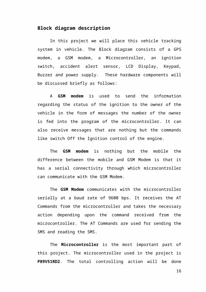
3.6 Block diagram
14
MICROCONTR-OLLER
P89V51RD2
KEYPAD(4x3)
LCD(16x2)
TTL to RS232
CONVERTER
GSMMODEM
BUZZER
ACCIDENTALERT
SENSOR
Block diagram description
In this project we will place this vehicle tracking system in vehicle. The
Block diagram consists of a GPS modem, a GSM modem, a Microcontroller,
an ignition switch, accident alert sensor, LCD Display, Keypad, Buzzer and
power supply. These hardware components will be discussed briefly as
follows:
A GSM modem is used to send the information regarding the status of
the ignition to the owner of the vehicle in the form of messages the number of
the owner is fed into the program of the microcontroller. It can also receive
messages that are nothing but the commands like switch Off the Ignition
control of the engine.
The GSM modem is nothing but the mobile the difference between the
mobile and GSM Modem is that it has a serial connectivity through which
microcontroller can communicate with the GSM Modem.
The GSM Modem communicates with the microcontroller serially at a
baud rate of 9600 bps. It receives the AT Commands from the microcontroller
and takes the necessary action depending upon the command received from
the microcontroller. The AT Commands are used for sending the SMS and
reading the SMS.
The Microcontroller is the most important part of this project. The
microcontroller used in the project is P89V51RD2. The total controlling action
will be done through this microcontroller. The Microcontroller receives the
data from the keypad and GSM Modem. It also authenticates the user
whether by checking the password entered by the user, if correct password is
entered then it allows the user to access the vehicle otherwise the ignition
switch is made OFF. The microcontroller can also switch OFF the Ignition
switch if a message is received to switch OFF the ignition part of the vehicle.
An Ignition switch plays the key role in the vehicle, for moving. If it is
in off condition, the vehicle does not move. In this project, for completely
15
stopping the vehicle we are just switched-off the ignition switch with the help
of the micro controller.
A LCD display is used at the output section to display the status of the
GSM and GPS. The LCD used in the project is 16X2. The maximum power
supply required to operate the hardware circuitry is 5V and 12V DC voltage.
A Buzzer is used to generate alert sound during the invalid access of
the vehicle
The Keypad used in the project is 4x3 matrix keypad. It is used to
enter password for switching on the Ignition of the vehicle. The ‘*’ is used for
cancelling the entered number and the ‘#’ key is used as the Enter key. After
entering the complete password the # key should be pressed.
16

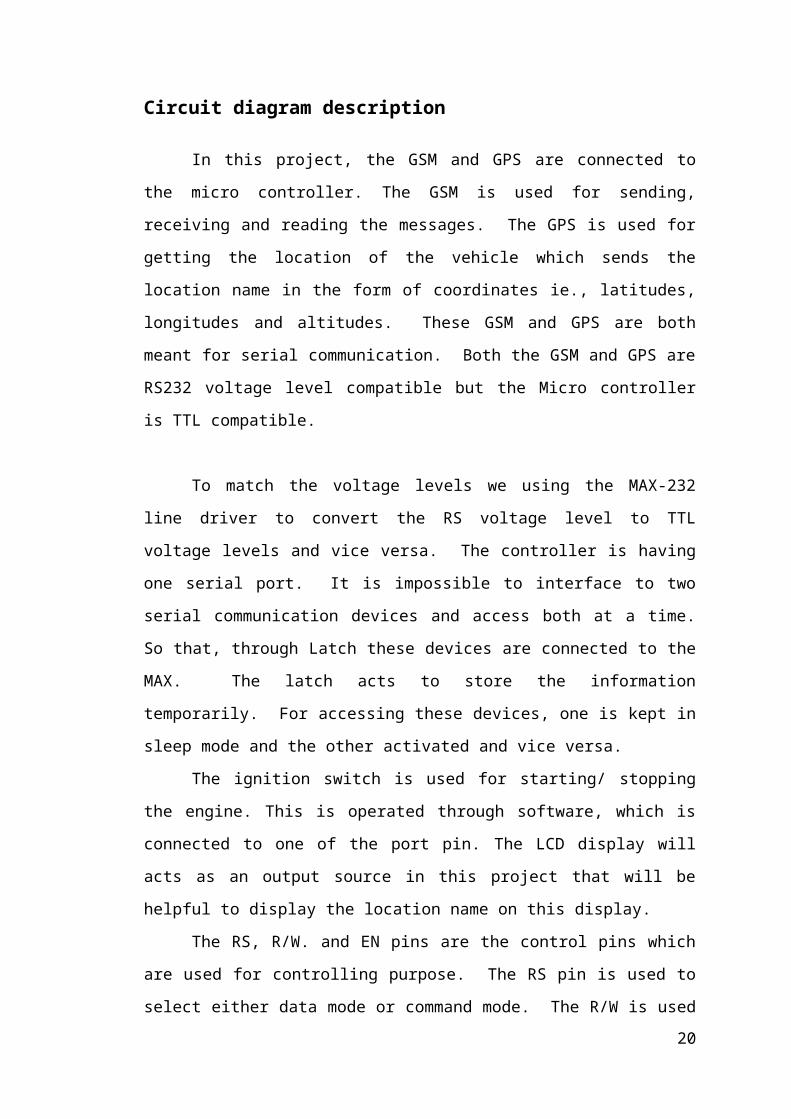
3.7 Circuit diagram
17

Circuit diagram description
In this project, the GSM and GPS are connected to the micro controller.
The GSM is used for sending, receiving and reading the messages. The GPS
is used for getting the location of the vehicle which sends the location name in
the form of coordinates ie., latitudes, longitudes and altitudes. These GSM
and GPS are both meant for serial communication. Both the GSM and GPS
are RS232 voltage level compatible but the Micro controller is TTL
compatible.
To match the voltage levels we using the MAX-232 line driver to
convert the RS voltage level to TTL voltage levels and vice versa. The
controller is having one serial port. It is impossible to interface to two serial
communication devices and access both at a time. So that, through Latch
these devices are connected to the MAX. The latch acts to store the
information temporarily. For accessing these devices, one is kept in sleep
mode and the other activated and vice versa.
The ignition switch is used for starting/ stopping the engine. This is
operated through software, which is connected to one of the port pin. The
LCD display will acts as an output source in this project that will be helpful to
display the location name on this display.
The RS, R/W. and EN pins are the control pins which are used for
controlling purpose. The RS pin is used to select either data mode or
command mode. The R/W is used to indicate that the LCD will acts as a
either read or write mode. The EN pin is used to enable the data. D0-D7 are
data pins used to get the data from the micro controller.
To operate the LCD display, which requires maximum of +5V DC
power supply. The power supply is used drive all the hardware components,
which are work at the maximum voltage of +5V DC. The 230V AC is a power
supply which is used for operate our general home appliance but the
hardware component which requires just +5V DC voltage. A step-down
transformer is used to step down the 230V AC to the required AC voltage and
thereafter it is meant for filtering with the help of a capacitor. Thereby, the
circuit is meant for the regulation to get the constant +5V DC.
18

3.8 Menu tree
19
ENTER THE
PASSWORD
CORRECT PASSWO
RD
INCORRECT
PASSWORD
AUTHENTICATIO
N
IGNITION ON/OFF
ACCIDENT ALERT CONTRO
L
IGNITION START
IGNITION STOP
ALERT MESSAGE SEND
TO OTHER
PERSON
BUZZER GETS ON
PERSON AUNTHENTICATE
D
PERSON UNAUNTHENTICATE
DINCORRE
CT PASSWO
RD
BUZZER GETS ON
Component List
20

COMPONENTS COST
GSM modem 2500/-
Microcontroller P89V51RD2 200/-
Crystal , Buzzer 10/-,10/-
LCD 16*2 150/-
Terminal block[32] 150/-
Regulator IC [1] 8/-
Relimate connector (16*1),(8*1) 35/-, 18/-
Serial cable 40/-
Wheels [60*4] 240/-
LED[4] 4/-
Miscellaneous 200/-
PCB development 800/-
MAX 232 15/-
IC 7805 10/-
Studs and screws 50/-
SMPS(12V) 180/-
Acrylic sheet 100/-
21

PCB designing
22

Fabrication
Printed circuit boards, or PCBs, form the core of electronic equipment
domestic and industrial. Some of the areas where PCBs are intensively used
are computers, process control, telecommunications and instrumentation.
Manufacturing
The manufacturing process consists of two methods; print and etch, and print,
plate and etch. The single sided PCBs are usually made using the print and
etch method. The double sided plate through hole (PTH) boards are made by
the print plate and etch method. The production of multi layer boards uses
both the methods. The inner layers are printed and etch while the outer layers
are produced by print, plate and etch after pressing the inner layers.
Penalization
Here the schematic transformed in to the working positive/negative films. The
circuit is repeated conveniently to accommodate economically as many
circuits as possible in a panel, which can be operated in every sequence of
subsequent steps in the PCB process. This is called penalization. For the
PTH boards, the next operation is drilling.
Drilling
PCB drilling is a state of the art operation. Very small holes are drilled with
high speed CNC drilling machines, giving a wall finish with less or no smear or
epoxy, required for void free through hole plating.
Plating
The heart of the PCB manufacturing process. The holes drilled in the board
are treated both mechanically and chemically before depositing the copper by
the electro less copper platting process.
23

Etching
Once a multiplayer board is drilled and electro less copper deposited, the
image available in the form of a film is transferred on to the outside by photo
printing using a dry film printing process. The boards are then electrolytic
plated on to the circuit pattern with copper and tin. The tin-plated deposit
serves an etch resist when copper in the unwanted area is removed by the
conveyor‘s spray etching machines with chemical etch ants. The etching
machines are attached to an automatic dosing equipment, which analyses
and controls etch ants concentrations
Design Rule
Rules followed while selecting artwork symbol are,
1. Minimum spacing between conductor and pad should be 0 .35 mm in 1:1
scale.
2. Minimum spacing between parallel conductors should be 0.4 mm in 1:1
scale.
3. The area of non-PTH solder pad should not be less than (5 sq.mm.).
4. The width of current carrying conductors should be determined for
maximum temperature, rise of 20 ْ�C.
General art work rules:
1. When there is higher conductor density assumes the conductors parallel to
any one of the edge of the board
2. When conductors have to be placed in other direction preference should be
given to the 45 � direction or to the 30 � / 60 � direction.
3. Whenever there is sufficient space available the conductors can be run in
any direction so as to achieve sorted possible interconnection.
4. As far as possible, design and the conductor on the solder pad. Conductor
forming sharp internal angles must be avoided.
24

5. When a member of conductor has to run between two pads the conductor
lines are run perpendicular w.r.to the center-to-center line of pair of pads.
6. Equally distributed spacing is to be provided when three or more
conductors run along a direction and / or between two pads.
7. Minimum spacing is provided when three or more lines run along a
direction and / or between two pads.
8. The diameter of solder pad should be approximately 8 times the drilled hole
diameter.
25

System testing and conclusion
26

Testing
Code Test:
1. The first step was to carry out the visual inspection of the PCB. This
means to check any short or cut in the tracks on PCB. Find any missing pads
if any where found on it. We did mechanical repair of the same.
2. The second step involved the continuity testing. This means to check that
the current is flowing through all the tracks.
3. Thirdly testing solder of socket crystal & reset circuitry.
Test Result :
[1] Give VCC and GND to microcontroller.
[2] Check voltage between 18 & 19 pins (XTAL 1, XTAL 2). It should be 2.5.
[3] Check available voltage pin 3.0-1.4. If all these voltage are coming then
the microcontroller is working properly.
[4] Check VCC and GND of LCD & write a RTN for display any message on
LCD if the message does not come check the supply again also check the
data lines for any opens or short.
µC Testing:
Initially the µC is given the power supply. All the respective ports and port pins
were checked when the signals were proper, it means that all the µC signal
were correct. If these signals are not proper, we can check the signals from
VCC ground, reset, circuit respectively. Even after the above test if the signals
are not proper it means that the purchased CPU is not functioning properly &
must be thrown.
1. We can put latch and memory in their respective sockets we wrote a
small program for the same then checked for numbers on port pin.
27

2. For the transmission of data stored in memory of µC. Various
parameters of communication port such as parity, data type baud rate
were checked before the transmission.
3. Accepting the data next step was to check that all the devices that are
connected and the program that was written to accept the data from
the µC is successful or not. ff not then the further modifications were
done in the program.
Conclusions
The “Car Security System using GSM” has been developed to the best of
knowledge and information made available to us. User friendliness has been
accented in this mini-project so that the user will be satisfied according to his
requirements.
With the knowledge of new techniques in ‘Electronics’ we are able to
make our life more comfortable. One such application of electronics is used in
“Car Security System using GSM”. The same circuit finds its use in many
more applications. By this Project we can track and block the vehicle.
This project provides a cheap and simple way to communicate with
user. We enjoyed every moment of working of this project and feel proud to hit
the Bulls Eye. Thus, we have implemented our engineering learning through
the project of “Car Security System using GSM”.
28

Source code
29

#include <reg51.h>#include <stdio.h>#include <string.h>#include "lcd.h"#include "serial.h"
sbit col1=P1^4;sbit col2=P1^5;sbit col3=P1^6;sbit row1=P1^0;sbit row2=P1^1;sbit row3=P1^2;sbit row4=P1^3;
sbit buzzer = P0^0;sbitignition_switch=P0^1;
/*--------------------Global declarations--------------------*/unsigned char code sto_password[4]="1234";unsigned char password[4]; //array for storing the password
unsigned char keycode; //for storing the key pressed codeunsigned char lcd_pos=0;bitpassword_complete=0; //flag for indicating that the key # is pressed/*------------------------------------------------------------*/
#define CR 0x0D
//definitations of the return value of the comparison#define UNKNOWN 0#define CMD_OK 1#define CMD_ERROR 2#define SEND_SUCCESS 3#define SEND_FAIL 4#define MSG_RECEIVED 5bitflag_cmd=0; //for indicating that the command is received from the modem//bit flagint=0;//for deciding the start of the command by detecting the presence of OA in the fisrt timebitrec_flag=0; //deciding whether command =0 or message=1 for the interrupt for storing thebitsend_start=0;bitmsg_start=0;//for indicating the start of the actual message from the received messagebitmsg_end=0; //for indicating the function that the entire message is received
unsigned char count_cr=0;unsigned char count_lf=0;
30

unsigned char rec_string[20]; //for storing the received command stringunsigned char len=0; //for storing the count value of the received strinngunsigned char rec_msg[35];unsigned char len_msg=0;unsigned char start_msg=0;unsigned char process[10];code unsigned char ok[3]="OK";
//for storing the message to be sentunsigned char code correct_msg[72] = "The password entered is correct and the ignition of vehicle is made ON\r\0";unsigned char code incorrect_msg[72] = "The password entered is incorrect the ignition of vehicle is made OFF\r\0";unsigned char code sms_correct_msg[85] = "The password sent through message is correct and the ignition of vehicle is made ON\r\0";unsigned char code sms_incorrect_msg[88] = "The password sent through message is incorrect and the ignition of vehicle is made OFF\r\0";unsigned char code stop_msg[] = "The ignition of the vehicle is stopped due to the stop command from the user";
voidsend_message(unsigned char msg_type);
/*---fucntion for generating delay in milli seconds----*//*input arguments : delay required in msec*/voiddelay_ms(unsigned intmsec){
unsignedint i;TMOD|=0X01;for(i=0;i<msec;i++){
TH0=0XFC;TL0=0X77;TR0=1;while(!TF0);TR0=0;TF0=0;
}}voidclear_flag(void){
len_msg=0;len=0;flag_cmd=0;count_cr=0;
31

count_lf=0;send_start=0;msg_start=0;start_msg=0;rec_flag=0;msg_end=0;
}//interrupt subroutine for serial receptionvoidreceive_data(void) interrupt 4 using 2{
if(RI){
RI=0;if(rec_flag==0&&send_start==0){
rec_string[len]=SBUF;if(rec_string[len]==0x0d)count_cr++;if(rec_string[len]==0x0a)count_lf++;if(count_cr==2&&count_lf==2)flag_cmd=1;len++;
}if(send_start==1){
rec_string[len]=SBUF;if(rec_string[len]==0X20)flag_cmd=1;len++;
}if(rec_flag==1){
rec_msg[len_msg]=SBUF;if(rec_msg[len_msg]==0X0A)start_msg++;if(msg_start){
if(rec_msg[len_msg]==CR){
rec_msg[len_msg]='\0';msg_end=1;
}elselen_msg++;
}
32

if(start_msg==2){
msg_start=1;}
}}
}
voidbuzzer_on(void){
unsigned char i;for(i=0;i<10;i++){
buzzer=0;delay_ms(250);buzzer=1;delay_ms(250);
}}/*-----------------------------------------------------------------function for comparing the received message with that of the password---------------------------------------------------------------------*/voidprocess_message(void){
if(!(strncmp(rec_msg,"1234 STOP",9))){
lclrscr();ignition_switch=0;lprintf(" Stop Vehicle ");gotoxy(2,1);lprintf(" Cmd Received ");delay_ms(1500);send_message(5);buzzer_on();
}
else if(!(strncmp(rec_msg,sto_password,4))){
lclrscr();ignition_switch=1;lprintf("Password Correct");delay_ms(1500);send_message(3);
}
else
33

{lclrscr();ignition_switch=0;lprintf("Password Incorrect");delay_ms(1500);send_message(4);buzzer_on();
}}voidread_message(unsigned char msg_id){
IE=0X00;rec_flag=1;send_string("AT+CMGR=");ser_tx(msg_id);ser_tx(CR);IE=0X90;while(!msg_end);IE=0x00;clear_flag();lprintf(rec_msg);delay(1000);IE=0x90;process_message();
}/*-----------------------------------------------------------------function for comparing the received command with that of the saved oneReturn value: the result status i.e. OK, ERROR,---------------------------------------------------------------------*/unsigned char process_data(void){
unsigned char i=0,j=0;while(flag_cmd==0);len=0;flag_cmd=0;count_cr=0;count_lf=0;
/*for removing the 0X0D AND 0X0A in the message and storing it in buffer*/
while(rec_string[i++]!= 0x0A);doprocess[j++]=rec_string[i++];while(rec_string[i]!=0x0D);process[j]='\0';//now comparing with the messagesif(!(strcmp(process,"OK")))return(CMD_OK);
34

else if(!(strcmp(process,"ERROR")))return(CMD_ERROR);
else if(!(strncmp(process,"+CMGSXXXXX",5)))return(SEND_SUCCESS);else if(!(strncmp(process,"+CMS:XXXXXXXX",4)))return(SEND_FAIL);
else if (!(strncmp(process,"+CMTI:XXXXXX",5)))return(MSG_RECEIVED);
elsereturn(UNKNOWN);
}
voidsend_message(unsigned char msg_type){
unsigned char i=0,j=0;unsigned char result;serial_init(9600);EA=1;ES=1;lclrscr();clear_flag();lprintf("Check Connection");gotoxy(2,1);send_string("AT\r");result=process_data();
switch(result){
case CMD_OK: lprintf("Modem connected"); break;case CMD_ERROR: lprintf("Error command"); break;
}delay_ms(500);lclrscr();lprintf("Check Network");send_string("AT+CREG=1\r");result=process_data();gotoxy(2,1);switch(result){
case CMD_OK: lprintf("NETWORK REGISTER"); break;case CMD_ERROR: lprintf("Error command"); break;
}delay_ms(500);lclrscr();lprintf("Sel. Text Mode");send_string("AT+CMGF=1\r");result=process_data();gotoxy(2,1);switch(result){
case CMD_OK: lprintf("TEXT MODE"); break;
35

case CMD_ERROR: lprintf("Error command"); break;}delay_ms(500);lclrscr();lprintf("Sending Message");send_start=1;send_string("AT+CMGS=\"+919769866207\"\r");while(flag_cmd==0);send_start=0;len=0;flag_cmd=0;count_cr=0;count_lf=0;delay(200);
/*for removing the 0X0D AND 0X0A in the message and storing it in buffer*/
if(msg_type==1){
send_string(correct_msg);ser_tx(0x1a);
}else if(msg_type==2){
send_string(incorrect_msg);ser_tx(0x1a);
}else if(msg_type==3){
send_string(sms_correct_msg);ser_tx(0x1a);
}else if(msg_type==4){
send_string(sms_incorrect_msg);ser_tx(0x1a);
}else if(msg_type==5){
send_string(stop_msg);ser_tx(0x1a);
}else if(msg_type==6){
}
result=process_data();gotoxy(2,1);switch(result)
36

{case CMD_ERROR: lprintf("Error command"); break;case SEND_SUCCESS: lprintf("Message Sent"); break;case SEND_FAIL : lprintf("Msg. Sending Fail"); break;
}clear_flag();delay_ms(500);
}
unsigned char keypad(void){
//scanning the first rowrow1=row2=row3=row4=1;row1=0;if(col1==0){
delay_ms(32);if(col1==0){
while(!col1);return(1);
}}if(col2==0){
delay_ms(32);if(col2==0){
while(!col2);return(2);
}}if(col3==0){
delay_ms(32);if(col3==0){
while(!col3);return(3);
}}//scanning the second rowrow1=row2=row3=row4=1;row2=0;if(col1==0){
delay_ms(32);if(col1==0){
37

while(!col1);return(4);
}}if(col2==0){
delay_ms(32);if(col2==0){
while(!col2);return(5);
}}if(col3==0){
delay_ms(32);if(col3==0){
while(!col3);return(6);
}}//scanning the third rowrow1=row2=row3=row4=1;row3=0;if(col1==0){
delay_ms(32);if(col1==0){
while(!col1);return(7);
}}if(col2==0){
delay_ms(32);if(col2==0){
while(!col2);return(8);
}}if(col3==0){
delay_ms(32);if(col3==0){
while(!col3);return(9);
38

}}//scanning the fourth rowrow1=row2=row3=row4=1;row4=0;if(col1==0){
delay_ms(32);if(col1==0){
while(!col1);return('*');
}}if(col2==0){
delay_ms(32);if(col2==0){
while(!col2);return(0);
}}if(col3==0){
delay_ms(32);if(col3==0){
while(!col3);return('#');
}}return('$');
}
voidlcd_keypad(unsigned char keycode){
if(keycode=='#')password_complete=1;
else if(keycode<=9){
if(lcd_pos<4){
password[lcd_pos++]=keycode+'0';gotoxy(2,lcd_pos);lcd_data((password[lcd_pos-1]));
}}else if(keycode=='*')
39

{lcd_pos--;gotoxy(2,(lcd_pos+1));lcd_data(' ');gotoxy(2,(lcd_pos+1));
}}//function for checking the entered passwordvoidpassword_check(void){
unsigned char i;for(i=0;i<4;i++){
if(password[i]==sto_password[i]);else
break;}if(i==4){
lclrscr();lprintf("Password Correct");delay_ms(1500);ignition_switch=1;send_message(1);
}else{
lclrscr();lprintf("Password Incorrect");delay_ms(1500);ignition_switch=0;send_message(2);buzzer_on();
}}
void main(void){
unsigned char result;P1=0xff;ignition_switch=0;buzzer=1;lcd_init();serial_init(9600);EA=1; ES=1;lprintf("VEHICLE SECURITY");gotoxy(2,1);
40

lprintf("SYSTEM USING GSM");delay_ms(1500);lclrscr();lprintf("Project Done By:");gotoxy(2,1);lprintf("****************");delay_ms(1500);lclrscr();lprintf("1. Abhishek ");gotoxy(2,1);lprintf("2. Anagha ");send_string("ATE0\r\0");delay_ms(1000);clear_flag();send_string("AT+CMGD=1\r\0");delay_ms(1000);clear_flag();lclrscr();lprintf("Enter Password");while(1){
keycode = keypad();if(keycode!='$'){
lcd_keypad(keycode);}if(password_complete){
lcd_pos=0;password_complete=0;password_check();delay(1000);lclrscr();lprintf("Enter Password");
}if(flag_cmd==1){
result=process_data();if(result==MSG_RECEIVED){
lclrscr();lprintf("Msg. Received");gotoxy(2,1);read_message('1');send_string("AT+CMGD=1\r\0");delay(1000);clear_flag();lclrscr();lprintf("Enter Password");
}
41

else{
lclrscr();lprintf("Msg not received");clear_flag();
}}if (accident == 0){
send_message(6)}
}}
42

Screen layout with test data and test results
43

Steps for executing the Keil programs:
Click on the KeiluVision Icon on Desktop
The following fig will appear
1. Click on the Project menu from the title bar
2. Then Click on New Project
44

3. Save the Project by typing suitable project name with no extension in u r own folder sited in either C:\ or D:\
4. Then Click on Save button above.
5. Select the component for u r project. i.e. Atmel……
6. Click on the + Symbol beside of Atmel
7. Select P89V51RD2 as shown below
45

8. Then Click on “OK”
9. The Following fig will appear
10. Then Click either YES or NO………mostly “NO”
11. Now your project is ready to USE
12. Now double click on the Target1, you would get another option
“Source group 1” as shown in next page.
46

13. Click on the file option from menu bar and select “new”
14. The next screen will be as shown in next page, and just maximize it
by double clicking on its blue boarder.
47

15. Now start writing program in either in “C” or “ASM”
16. For a program written in Assembly, then save it with extension “.
asm” and for “C” based program save it with extension “ .C”
17. Now right click on Source group 1 and click on “Add files to Group
Source”
48

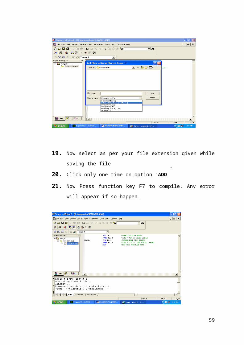
18. Now you will get another window, on which by default “C” files will
appear.
19. Now select as per your file extension given while saving the file
20. Click only one time on option “ADD”
21. Now Press function key F7 to compile. Any error will appear if so
happen.
49

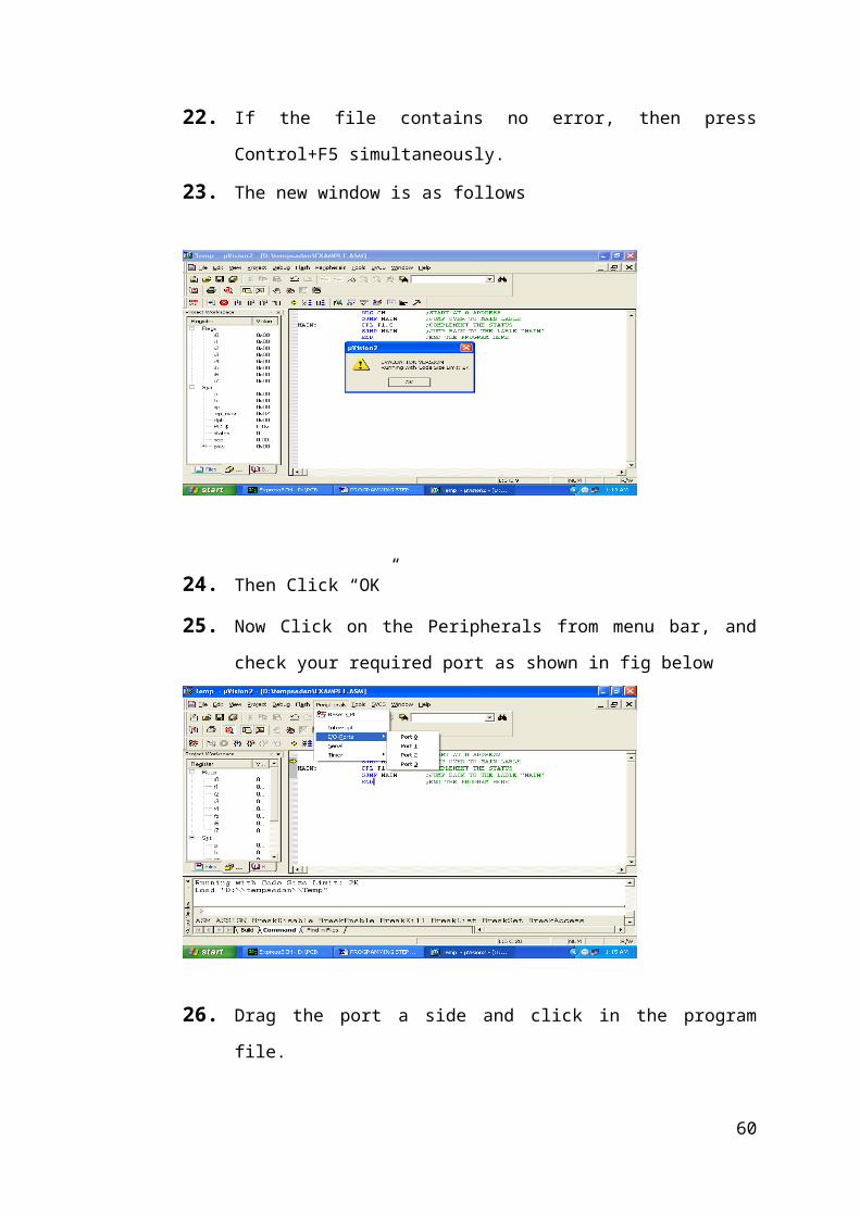
22. If the file contains no error, then press Control+F5 simultaneously.
23. The new window is as follows
24. Then Click “OK”
25. Now Click on the Peripherals from menu bar, and check your
required port as shown in fig below
50

26. Drag the port a side and click in the program file.
27. Now keep Pressing function key “F11” slowly and observe.
28. You are running your program successfully
51

Results
52

53

54

55

56

Report layouts
57

Datasheet Of Components
1.LCD
58
2.Rectifier
59
3.Diodes
60

61

4.Pin Configuration of 89V51RD2
Pin
62

Details:
89V51RD is 40 pin IC with four ports. Pin diagram of microcontroller is shown in
Fig.
VCC - - Supply voltage..
VSS - - Ground.
Port 0Port 0
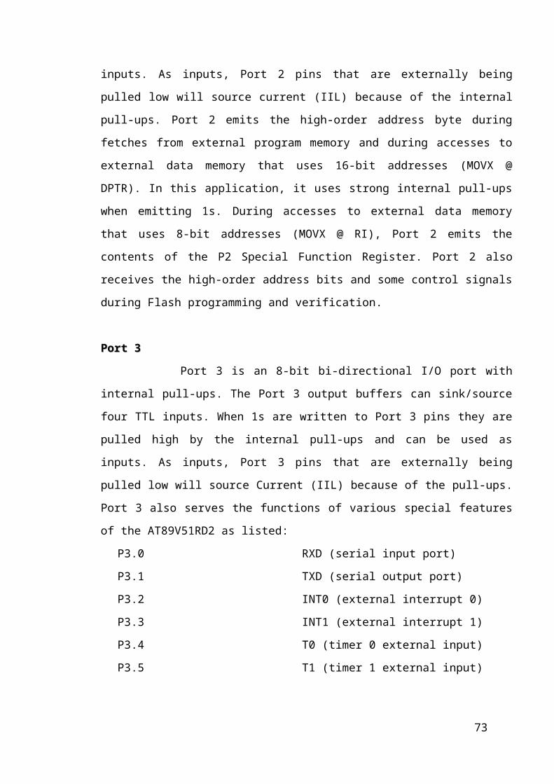
Port 0 is an 8-bit open-drain bi-directional I/O port. As an output port, each pin
can sink eight TTL inputs. When 1s are written to port 0 pins, the pins can be used
as high impedance inputs. Port 0 may also be configured to be the multiplexed low
order address/data bus during accesses to external program and data memory. In
this mode P0 has internal pull-ups. Port 0 also receives the code bytes during
Flash programming, and outputs the code bytes during program verification.
External pull-ups are required during program verification.
Port 1 Port 1
Port 1 is an 8-bit bi-directional I/O port with internal pull-ups. The Port 1 output
buffers can sink/source four TTL inputs. When 1s are written to Port 1 pins they are
pulled high by the internal pull-ups and can be used as inputs. As inputs, Port 1
pins that are externally being pulled low will source current (IIL) because of the
internal pull-ups. Port 1 also receives the low-order address bytes during Flash
programming and verification.
Port 2Port 2
Port 2 is an 8-bit bi-directional I/O port with internal pull-ups. The Port 2 output
buffers can sink/source four TTL inputs. When 1s are written to Port 2 pins they are
pulled high by the internal pull-ups and can be used as inputs. As inputs, Port 2
pins that are externally being pulled low will source current (IIL) because of the
internal pull-ups. Port 2 emits the high-order address byte during fetches from
external program memory and during accesses to external data memory that uses
16-bit addresses (MOVX @ DPTR). In this application, it uses strong internal pull-
ups when emitting 1s. During accesses to external data memory that uses 8-bit
addresses (MOVX @ RI), Port 2 emits the contents of the P2 Special Function
63

Register. Port 2 also receives the high-order address bits and some control signals
during Flash programming and verification.
Port 3Port 3
Port 3 is an 8-bit bi-directional I/O port with internal pull-ups. The Port 3
output buffers can sink/source four TTL inputs. When 1s are written to Port 3 pins
they are pulled high by the internal pull-ups and can be used as inputs. As inputs,
Port 3 pins that are externally being pulled low will source Current (IIL) because of
the pull-ups. Port 3 also serves the functions of various special features of the
AT89V51RD2 as listed:
P3.0 RXD (serial input port)
P3.1 TXD (serial output port)
P3.2 INT0 (external interrupt 0)
P3.3 INT1 (external interrupt 1)
P3.4 T0 (timer 0 external input)
P3.5 T1 (timer 1 external input)
P3.6 WR (external data memory write strobe)
P3.7 RD (external data memory read strobe)
Port 3 also receives some control signals for Flash programming and
verification.
RST –RST –
Reset input. A high on this pin for two machine cycles while the oscillator is
running resets the device.
ALE/ PROGALE/ PROG
Address Latch Enable output pulse for latching the low byte of the address
during accesses to external memory. This pin is also the program pulse input
(PROG) during Flash programming. In normal operation ALE is emitted at a
constant rate of 1/6 the oscillator frequency, and may be used for external timing or
clocking purposes. Note, however, that one ALE pulse is skipped during each
access to external Data Memory. If desired, ALE operation can be disabled by
setting bit 0 of SFR location 8EH. With the bit set, ALE is active only during a
64

MOVX or MOVC instruction. Otherwise, the pin is weakly pulled high. Setting the
ALE-disable bit has no effect if the microcontroller is in external execution mode.
PSENPSEN
Program Store Enable is the read strobe to external program memory. When
the 89V51RD2FA is executing code from external program memory, PSEN is
activated twice each machine cycle, except that two PSEN activations are skipped
during each access to external data memory.
EA/VPP EA/VPP
External Access Enable. EA must be strapped to GND in order to enable the
device to fetch code from external program memory locations starting at 0000H up
to FFFFH. Note, however, that if lock bit 1 is programmed, EA will be internally
latched on reset. EA should be strapped to VCC for internal program executions.
This pin also receives the 12-volt programming enable voltage (VPP) during Flash
programming, for parts that require 12-volt VPP.
Oscillator and Clock Details:Oscillator and Clock Details:
Oscillator Characteristics:
XTAL1 and XTAL2 are the input and output, respectively, of an
inverting amplifier, which can be configured for use as an on-chip oscillator,
as shown in Figs 6.1 Either a quartz crystal or ceramic resonator may be
used. To drive the device from an external clock source, XTAL2 should be left
unconnected while XTAL1 is driven as shown in Figure 6.2. There are no
requirements on the duty cycle of the external clock signal, since the input to
the internal clocking circuitry is through a divide-by-two flip-flop, but minimum
and maximum voltage high and low time specifications must be observed.
65

Fig 6.1 Oscillator Connections Fig 6.2 External Clock Drive
Configuration
XTAL1
Input to the inverting oscillator amplifier and input to the internal clock
operating circuit.
XTAL2
Output from the inverting oscillator amplifier.
3.1.5 Transmission in 89V51RD2:3.1.5 Transmission in 89V51RD2:
89V51RD2 has a serial data communication circuit that uses register SBUF to
hold data. Register SCON controls data communication. Register PCON controls
data rates. Pins RxD (p3.0) and TxD(3.1) connect to serial data network. SBUF is
physically two registers, one is writing only i.e. to hold data to be transmitted out of
microcontroller via TxD. The other is read only and holds received data from an
external transmitting source via RxD.
Whenever a data byte is transmitted T1 flag is set and so program is
interrupted to transmit another byte of data. The main program is interrupted only
serial port interrupt is 1E SFR is enable.
The data transmission steps are:
Initially the T1 flag is reset.
Data to be transmitted must be written into SBUF.
As soon as data is transmitted the T1 flag is set and main program is
interrupted to execute ISR.
In the ISR T1 flag is reset .another data is written in SBUF register.
External Access Enable. EA must be strapped to GND in order to
enable the device to fetch code from external program memory locations
starting at 0000H up to FFFFH.
Note, however, that if lock bit 1 is programmed, EA will be internally
latched on reset. EA should be strapped to VCC for internal program
executions. This pin also receives the 12-volt programming enable voltage
(VPP) during Flash programming, for parts that require 12-volt VPP.
XTAL1:
66

Input to the inverting oscillator amplifier and input to the internal clock
operating circuit.
XTAL2:
Output from the inverting oscillator amplifier.
8051 Register Banks and Stack
RAM memory space allocation in the 8051
There are 128 bytes of RAM in the 8051. The 128 bytes of RAM inside
the 8051 are assigned addresses 00 to7FH. These 128 bytes are divided into
three different groups as follows:
1. A total of 32 bytes from locations 00 to 1FH hex are set aside for
register banks and the stack.
2. A total of 16 bytes from locations 20 to 2FH hex are set aside for
bit-addressable read/write memory.
3. A total of 80 bytes from locations 30H to 7FH are used for read and
write storage, or what is normally called Scratch pad. These 80
locations of RAM are widely used for the purpose of storing data
and parameters nu 8051 programmers.
67

Default register bank
Register bank 0; that is, RAM locations 0, 1,2,3,4,5,6, and 7 are
accessed with the names R0, R1, R2, R3, R4, R5, R6, and R7 when
programming the 8051.
FIG 8: RAM Allocation in the 8051
PSW Register (Program Status Word)
This is one of the most important SFRs. The Program Status Word (PSW)
contains several status bits that reflect the current state of the CPU. This
register contains: Carry bit, Auxiliary Carry, two register bank select bits,
Overflow flag, parity bit, and user-definable status flag. The ALU automatically
changes some of register’s bits, which is usually used in regulation of the
program performing.
P - Parity bit. If a number in accumulator is even then this bit will be
automatically set (1), otherwise it will be cleared (0). It is mainly used during
data transmission and receiving via serial communication.
68

OV Overflow occurs when the result of arithmetical operation is greater than
255 (decimal), so that it cannot be stored in one register. In that case, this bit
will be set (1). If there is no overflow, this bit will be cleared (0).
RS0, RS1 - Register bank select bits. These two bits are used to select one
of the four register banks in RAM. By writing zeroes and ones to these bits, a
group of registers R0-R7 is stored in one of four banks in RAM.
RS1 RS2 Space in RAM
0 0 Bank0 00h-07h
0 1 Bank1 08h-0Fh
1 0 Bank2 10h-17h
1 1 Bank3 18h-1Fh
F0 - Flag 0. This is a general-purpose bit available to the user.
AC - Auxiliary Carry Flag is used for BCD operations only.
CY - Carry Flag is the (ninth) auxiliary bit used for all arithmetical operations
and shift instructions.
DPTR Register (Data Pointer)
These registers are not true ones because they do not physically exist. They
consist of two separate registers: DPH (Data Pointer High) and (Data Pointer
Low). Their 16 bits are used for external memory addressing. They may be
handled as a 16-bit register or as two independent 8-bit registers. Besides,
the DPTR Register is usually used for storing data and intermediate results,
which have nothing to do with memory locations.
69

SP Register (Stack Pointer)
The stack is a section of RAM used by the CPU to store information
temporily. This information could be data or an address. The CPU needs this
storage area since there are only a limited number of registers.
How stacks are accessed in the 8051
If the stack is a section of RAM, there must be registers inside the CPU
to point to it. The register used to access the stack is called the SP (Stack
point) Register. The stack pointer in the 8051 is only 8 bits wide; which
means that it can take values of 00 to FFH. When the 8051 is powered up,
the SP register contains value 07. This means that RAM location 08 is the
first location used for the stack by the 8051. The storing of a CPU register in
the stack is called a PUSH, and pulling the contents off the stack back into a
CPU register is called a POP. In other words, a register is pushed onto the
stack to save it and popped off the stack to retrieve it. The job of the SP is
very critical when push and pop actions are performed.
Program counter:
The important register in the 8051 is the PC (Program counter). The
program counter points to the address of the next instruction to be executed.
As the CPU fetches the opcode from the program ROM, the program counter
is incremented to point to the next instruction. The program counter in the
8051 is 16bits wide. This means that the 8051 can access program
addresses 0000 to FFFFH, a total of 64k bytes of code. However, not all
70

members of the 8051 have the entire 64K bytes of on-chip ROM installed, as
we will see soon.
Serial Communication:
Serial data communication uses two methods, asynchronous and
synchronous. The synchronous method transfers a block of data at a time,
while the asynchronous method transfers a single byte at a time.
In data transmission if the data can be transmitted and received, it is a
duplex transmission. This is in contrast to simplex transmissions such as with
printers, in which the computer only sends data. Duplex transmissions can be
half or full duplex, depending on whether or not the data transfer can be
simultaneous. If data is transmitted one way at a time, it is referred to as half
duplex. If the data can go both ways at the same time, it is full duplex. Of
course, full duplex requires two wire conductors for the data lines, one for
transmission and one for reception, in order to transfer and receive data
simultaneously.
Asynchronous serial communication and data framing
The data coming in at the receiving end of the data line in a serial data
transfer is all 0s and 1s; it is difficult to make sense of the data unless the
sender and receiver agree on a set of rules, a protocol, on how the data is
packed, how many bits constitute a character, and when the data begins and
ends.
Start and stop bits
Asynchronous serial data communication is widely used for character-
oriented transmissions, while block-oriented data transfers use the
synchronous method. In the asynchronous method, each character is placed
between start and stop bits. This is called framing. In the data framing for
asynchronous communications, the data, such as ASCII characters, are
packed between a start bit and a stop bit. The start bit is always one bit, but
the stop bit can be one or two bits. The start bit is always a 0 (low) and the
stop bit (s) is 1 (high).
71

Data transfer rate
The rate of data transfer in serial data communication is stated in bps
(bits per second). Another widely used terminology for bps is baud rate.
However, the baud and bps rates are not necessarily equal. This is due to the
fact that baud rate is the modem terminology and is defined as the number of
signal changes per second. In modems a single change of signal, sometimes
transfers several bits of data. As far as the conductor wire is concerned, the
baud rate and bps are the same, and for this reason we use the bps and baud
interchangeably.
RS232 Standards
To allow compatibility among data communication equipment made by
various manufacturers, an interfacing standard called RS232 was set by the
Electronics Industries Association (EIA) in 1960. In 1963 it was modified and
called RS232A. RS232B AND RS232C were issued in 1965 and 1969,
respectively. Today, RS232 is the most widely used serial I/O interfacing
standard. This standard is used in PCs and numerous types of equipment.
However, since the standard was set long before the advert of the TTL logic
family, its input and output voltage levels are not TTL compatible. In RS232,
a 1 is represented by -3 to -25V, while a 0 bit is +3 to +25V, making -3 to +3
undefined. For this reason, to connect any RS232 to a micro controller
system we must use voltage converters such as MAX232 to convert the TTL
logic levels to the RS232 voltage levels, and vice versa. MAX232 IC chips
are commonly referred to as line drivers.
RS232 pins
RS232 cable, commonly referred to as the DB-25 connector. In
labeling, DB-25P refers to the plug connector (male) and DB-25S is for the
socket connector (female). Since not all the pins are used in PC cables, IBM
introduced the DB-9 Version of the serial I/O standard, which uses 9 pins
only, as shown in table.
(Out of computer and exposed end of cable)
72
Pin Functions:
Pi
n
Description
1 Data carrier detect (DCD)
2 Received data (RXD)
3 Transmitted data (TXD)
4 Data terminal ready(DTR)
5 Signal ground (GND)
6 Data set ready (DSR)
7 Request to send (RTS)
8 Clear to send (CTS)
9 Ring indicator (RI)
Note: DCD, DSR, RTS and CTS are active low pins.
The method used by RS-232 for communication allows for a simple
connection of three lines: Tx, Rx, and Ground. The three essential signals for
2-way RS-232
8051 connection to RS232
The RS232 standard is not TTL compatible; therefore, it requires a line
driver such as the MAX232 chip to convert RS232 voltage levels to TTL
levels, and vice versa. The interfacing of 8051 with RS232 connectors via the
MAX232 chip is the main topic.
The 8051 has two pins that are used specifically for transferring and
receiving data serially. These two pins are called TXD and RXD and a part of
the port 3 group (P3.0 and P3.1). pin 11 of the 8051 is assigned to TXD and
pin 10 is designated as RXD. These pins are TTL compatible; therefore, they
require a line driver to make them RS232 compatible. One such line driver is
the MAX232 chip.
Since the RS232 is not compatible with today’s microprocessors and
microcontrollers, we need a line driver (voltage converter) to convert the
RS232’s signals to TTL voltage levels that will be acceptable to the 8051’s
73

TXD and RXD pins. One example of such a converter is MAX232 from
Maxim Corp. The MAX232 converts from RS232 voltage levels to TTL
voltage levels, and vice versa.
Fig 11: Interfacing of MAX-232 to controller
Interrupts in the 8051:
In reality, only five interrupts are available to the user in the 8051, but many
manufacturers’ data sheets state that there are six interrupts since they
include reset .the six interrupts in the 8051 are allocated as above.
1. Reset. When the reset pin is activated, the 8051 jumps to address
location 0000.this is the power-up reset.
2. Two interrupts are set aside for the timers: one for Timer 0 and one for
Timer 1.Memory location 000BH and 001BH in the interrupt vector
table belong to Timer 0 and Timer 1, respectively.
3. Two interrupts are set aside for hardware external harder interrupts.
Pin number 12(P3.2) and 13(P3.3) in port 3 is for the external hardware
interrupts INT0 and INT1, respectively. These external interrupts are
also referred to as EX1 and EX2.Memory location 0003H and 0013H in
the interrupt vector table are assigned to INT0 and INT1, respectively.
4. Serial communication has a single interrupt that belongs to both
receive and transmit. The interrupt vector table location 0023H belongs
to this interrupt.
Interrupt Enable Register
D7 D6 D5 D4 D3 D2 D1 D0
74
EA -- ET2 ES ET1 EX1 ET0 EX0

EA IE.7 disables all interrupts. If EA=0, no interrupts is
acknowledged.
If EA=1, each interrupt source is individually enabled
disabled
By setting or clearing its enable bit.
-- IE.6 Not implemented, reserved for future use.*
ET2 IE.5 Enables or disables Timer 2 overflow or capture interrupt (8052
only).
ES IE.4 Enables or disables the serial ports interrupt.
ET1 IE.3 Enables or disables Timers 1 overflow interrupt
EX1 IE.2 Enables or disables external interrupt 1.
ET0 IE.1 Enables or disables Timer 0 overflow interrupt.
EX0 IE.0 Enables or disables external interrupt 0.
5.GSM Modem SIM300
75

6.MAX-232
76

MAX232 to RS232 DB9 Connection as a DCE
MAX232 Pin Nbr. MAX232 Pin Name Signal Voltage DB9 Pin
7 T2out CTS RS-232 7
8 R2in RTS RS-232 8
9 R2out RTS TTL n/a
10 T2in CTS TTL n/a
11 T1in TX TTL n/a
12 R1out RX TTL n/a
13 R1in TX RS-232 3
14 T1out RX RS-232 2
15 GND GND 0 5
77
MAX232(A) external Capacitors
Capacitor + Pin - Pin Remark
C1 1 3
C2 4 5
C3 2 16
C4 GND 6This looks non-intuitive, but because pin 6 is
on -10V, GND gets the + connector, and not the -
C5 16 GND

References/ bibliography/websites
used
Bibliography
The 8051 Micro controller and Embedded Systems
-Muhammad Ali MazidiJanice GillispieMazidi
The 8051 Micro controller Architecture,Programming & Applications
-Kenneth J.Ayala
Fundamentals of Micro processors and Micro computers
-B.Ram
78

Micro processor Architecture, Programming& Applications
-Ramesh S.Gaonkar
Electronic Components
-D.V.Prasad
Wireless Communications - Theodore S. Rappaport
Mobile Tele Communications - William C.Y. Lee
References on the Web:
www.national.com www.atmel.com www.microsoftsearch.com www.geocities.com http://tycho.usno.navy.mil/gpscurr.html
Annexure79

Applications
Using this technique we can take our car safe from theft.
If our vehicle is suppose to be stolen by any theft then within some minutes we can find it.
Rather than break & steering lock it is best way to stop engine remotely .
Future scope
In next some days we can use GPS system & finds exact location of vehicle.
80

We can also use GPRS system to implement this technique worldwide.
We can use DTMF technique along with GSM modem to secure our car.
We can also implement using thumb or fingerprint base technology.
Abbreviations
ACC - AccumulatorB - B RegisterPSW - Program Status WordSP - Stack PointerDPTR - Data pointerDPL - Low byteDPH - High byteP0 - Port 0P1 - Port 1P2 - Port 2P3 - Port 3IE - Interrupt Enable controlIP - Interrupt Priority controlTMOD - Timer/Counter Mode controlTCON - Timer/Counter controlT2CON - Timer/counter 2 controlT2MOD - Timer/counter mode2 controlTH0 - Timer/counter 0high byteTL0 - Timer/counter 0 low byteTH1 - Timer/counter 1 high byteTL1 - Timer/counter 1 low byteTH2 - Timer/counter 2 high byteTL2 - Timer/counter 2 low byteRCAP2H - T/C 2 capture register high byteRCAP2L - T/C 2 capture register low byteSCON - Serial controlSBUF - Serial data bufferPCON - Power controlGSM -Global System for Mobile CommunicationsPCB - Printed circuit BoardSFR - Special function registersWAAS - Wide Area Augmentation SystemLCD - Liquid Crystal Display
81