Capacitance-Voltage Study on the Effects of Low Energy ...
144
Air Force Institute of Technology Air Force Institute of Technology AFIT Scholar AFIT Scholar Theses and Dissertations Student Graduate Works 3-11-2005 Capacitance-Voltage Study on the Effects of Low Energy Electron Capacitance-Voltage Study on the Effects of Low Energy Electron Radiation on Al Radiation on Al 0.27 0.27 Ga Ga 0.73 0.73 N/GaN High Electron Mobility Transistor N/GaN High Electron Mobility Transistor Thomas D. Jarzen Follow this and additional works at: https://scholar.afit.edu/etd Part of the Electrical and Electronics Commons, and the Nuclear Engineering Commons Recommended Citation Recommended Citation Jarzen, Thomas D., "Capacitance-Voltage Study on the Effects of Low Energy Electron Radiation on Al 0.27 Ga 0.73 N/GaN High Electron Mobility Transistor" (2005). Theses and Dissertations. 3737. https://scholar.afit.edu/etd/3737 This Thesis is brought to you for free and open access by the Student Graduate Works at AFIT Scholar. It has been accepted for inclusion in Theses and Dissertations by an authorized administrator of AFIT Scholar. For more information, please contact richard.mansfield@afit.edu.
Transcript of Capacitance-Voltage Study on the Effects of Low Energy ...

Air Force Institute of Technology Air Force Institute of Technology
AFIT Scholar AFIT Scholar
Theses and Dissertations Student Graduate Works
3-11-2005
Capacitance-Voltage Study on the Effects of Low Energy Electron Capacitance-Voltage Study on the Effects of Low Energy Electron
Radiation on AlRadiation on Al0.270.27GaGa0.730.73N/GaN High Electron Mobility Transistor N/GaN High Electron Mobility Transistor
Thomas D. Jarzen
Follow this and additional works at: https://scholar.afit.edu/etd
Part of the Electrical and Electronics Commons, and the Nuclear Engineering Commons
Recommended Citation Recommended Citation Jarzen, Thomas D., "Capacitance-Voltage Study on the Effects of Low Energy Electron Radiation on Al0.27Ga0.73N/GaN High Electron Mobility Transistor" (2005). Theses and Dissertations. 3737.
https://scholar.afit.edu/etd/3737
This Thesis is brought to you for free and open access by the Student Graduate Works at AFIT Scholar. It has been accepted for inclusion in Theses and Dissertations by an authorized administrator of AFIT Scholar. For more information, please contact [email protected].

CAPACITANCE-VOLTAGE STUDY ON THE EFFECTS OF LOW ENERGY
ELECTRON RADIATION ON Al0.27Ga0.73N/GaN HIGH ELECTRON MOBILITY TRANSISTORS
THESIS
Thomas D. Jarzen, Major, USA
AFIT/GNE/ENP/05-05
DEPARTMENT OF THE AIR FORCE AIR UNIVERSITY
AIR FORCE INSTITUTE OF TECHNOLOGY
Wright-Patterson Air Force Base, Ohio
APPROVED FOR PUBLIC RELEASE; DISTRIBUTION UNLIMITED

The views expressed in this thesis are those of the author and do not reflect the official policy or position of the United States Air Force, Department of Defense, or the United States Government.

AFIT/GNE/ENP/05-05
CAPACITANCE-VOLTAGE STUDY ON THE EFFECTS OF LOW ENERGY ELECTRON RADIATION ON Al0.27Ga0.73N/GaN HIGH ELECTRON MOBILITY
TRANSISTORS
THESIS
Presented to the Faculty
Department of Engineering Physics
Graduate School of Engineering and Management
Air Force Institute of Technology
Air University
Air Education and Training Command
In Partial Fulfillment of the Requirements for the
Degree of Master of Science (Nuclear Science)
Thomas D. Jarzen
Major, USA
March 2005
APPROVED FOR PUBLIC RELEASE; DISTRIBUTION UNLIMITED
CAPACITANCE-VOLTAGE STUDY ON THE EFFECTS OF LOW ENERGY ELECTRON RADIATION ON Ab2fiso.73NIGaN HIGH ELECTRON MOBILITY
TRANSISTORS
Thomas D. J a m n Major, USA, B.S., M.S.
Approved:
@r. Gary C. Farlow (Member)
DL ~aufdlsbditis (Member)
//,I65 date
date

AFIT/GNE/ENP/05-05
Abstract
The effects of radiation on semiconductors are extremely important to the
Department of Defense since the majority of the defense informational, navigational and
communications systems are now satellite-based. Due to the high radiation tolerance of
gallium nitride and a plethora of high temperature, high power and high frequency
applications, the prospect that gallium nitride based devices will become key components
in a multitude of military satellite-based systems is highly probable.
AlGaN/GaN HEMTs were irradiated at low temperature (~80 K) by 0.45 – 0.8
MeV electrons up to fluences of 1×10¹⁵ e-/cm2. Following irradiation, low temperature
capacitance-voltage measurements were recorded providing fluence-dependent
measurements; additionally low-temperature post-irradiation capacitance-voltage
measurements were recorded at twenty-four hour intervals up to 72 hours in order to
investigate the room temperature annealing process. Using previously irradiated devices,
the effects of a 9 month and 12 month room temperature anneal were also considered.
Capacitance-voltage measurements indicate that low energy electron radiation
results in an increase in the transistor channel drain current. These increases occur both at
low and room temperature. The mechanism, clearly shown through capacitance-voltage
measurements, causing the increase in drain current is an increase in the carrier
concentration in the 2DEG. This result is due to donor electrons from a nitrogen vacancy
in the gallium nitride. The devices begin to anneal immediately and show almost
complete recovery after 72 hours.
iv

AFIT/GNE/ENP/05-05
To my family
v

Acknowledgments
Dr. James Petrosky, my advisor, has been an invaluable asset and mentor by
providing vital technical knowledge, experience and assistance. Truly, without his help
this project would never have reached completion. Prior to taking his class radiation
effects on electronics, I did not even know what a semiconductor was other than
something that controlled a microwave oven. He has been an outstanding guide through a
strange land.
Dr. Gary Farlow of the Wright State University was responsible for providing the
means by which the experiments were carried out. Without the timeless efforts he
provided towards repairing, maintaining and running the Van de Graff facility during the
experiments, there would be no results to present.
Renate Hannaford of the AFIT library was responsible for assisting in a massive
literature search on radiation interaction in GaN and AlGaN. Without her assistance,
much of this document would have been incomplete.
Larry Callaghan was responsible for wafer dicing and packaging. His consistently
quick turn-around on packaging requests proved to be integral, allowing experiments to
be conducted when needed.
My Wife, Daughters and Sons, and other family members and friends continuously
provided me with the support and encouragement that kept me going through this long
and arduous process. Now all my time will once again be theirs.
And, to DMJ and SAJ for without them none of this would have been possible.
Illigitimi non carborundum sunt!
vi

Table of Contents
Page Abstract .............................................................................................................................. iv
Acknowledgments.............................................................................................................. vi
List of Figures .................................................................................................................... ix
List of Tables .................................................................................................................... xv
List of Symbols ................................................................................................................ xvi
List of Abbreviations and Acronyms............................................................................. xviii
I. Introduction ..................................................................................................................... 1
Background..................................................................................................................... 1 Problem Statement .......................................................................................................... 9 Hypothesis....................................................................................................................... 9 Objectives ....................................................................................................................... 9 Scope............................................................................................................................... 9 Approach....................................................................................................................... 10 Assumptions.................................................................................................................. 11 Sequence of Presentation .............................................................................................. 12
II. Literature Review......................................................................................................... 13
Purpose.......................................................................................................................... 13 Fundamentals of Gallium Nitride heterostructures....................................................... 13 Importance of Aluminum Gallium Nitride and Gallium Nitride .................................. 14 Radiation Effects of Protons on AlGaN / GaN............................................................. 17 Radiation Effects of Electrons in AlGaN / GaN........................................................... 22 Capacitance-Voltage Measurements............................................................................. 26 Research Justification ................................................................................................... 31
III. Theory ......................................................................................................................... 32
CV Measurements......................................................................................................... 32 Heterostructure Energy Band Diagrams ....................................................................... 39 Performing CV Measurements ..................................................................................... 42 Radiation Interaction in GaN........................................................................................ 44 Expected Radiation Effects on C-V Curves.................................................................. 47
vii

IV. Experimental Procedures ............................................................................................ 52
Transistor Background.................................................................................................. 52 Pre-Irradiation Characterization.................................................................................... 56 Irradiation Experiments ................................................................................................ 61
V. Experimental Results ................................................................................................... 73
Irradiation Experiment: Sample A19 ............................................................................ 73 Irradiation Experiments: Sample A16 .......................................................................... 74 Irradiation Experiments: Sample A1 ............................................................................ 76 Irradiation Experiments: Sample A2 ............................................................................ 84 Previously Irradiated Samples: A0408 and A0409....................................................... 90 Analysis and Discussion ............................................................................................... 96
VI. Conclusions and Recommendations ......................................................................... 104
Conclusions................................................................................................................. 104 Recommendations for Further Work .......................................................................... 105
Appendix A – Visual Basic Data Acquisition Program.................................................. 107
Appendix B – Pre-characterization C-V Plots (80K / 330K) ......................................... 115
Appendix C – Carrier Concentration Calculations ......................................................... 117
Bibliography ................................................................................................................... 118
viii

ix
List of Figures
Figure Page
1. USchematic representation of the trapped electron radiation belts [3]. U......................3
2. UCross-Section of a typical AlGaN/GaN HEMT [17]. U ..............................................7
3. UCharge carrier velocity versus electric field for various semiconductors [10].U .....15
4. UTransconductance versus gate-source voltage for AlGaN/AlN/GaN HEMTs before and after 1.8 MeV proton irradiation with fluences from 1 × 10UPU
13UPU cmUPU
-2UPU
to 1 × 10UPU
15UPU cmUPU
-2UPU [30].U..............................................................................................19
5. UCommon-source drain current as a function of gate voltage and transconductance of the same transistor pre-irradiation (solid line), post-10UPU
12UPU cmUPU
-2UPU fluence (dashed line), and post-5 × 10UPU
13UPU cmUPU
-2UPU fluence
(dotted line) [13].U ...................................................................................................20
6. UTransfer characteristics for AlGaN/GaN HEMTs before and after 1.8 MeV proton irradiation at various fluences [31].U............................................................21
7. UTransfer characteristics for AlGaN/GaN HEMTs before and after 105-MeV proton irradiation at different fluences [31].U..........................................................22
8. USample A0409 FatFET First Irradiation: Change in I-V Curves at LiN Temperature (0.45 MeV Electrons) [21].U ..............................................................24
9. USample A0409 FatFET Second Irradiation: Change in I-V Curves at LiN Temperature (0.45 MeV Electrons) [21].U ..............................................................25
10. UTypical plot of the variation of the capacitance (pF) of a 500 µm x 500 µm capacitor versus gate voltage (VUBUGUBU) ranging from –4.7 to +4.7 volts [33].U .............27
11. UTypical C-V curve measured in darkness at room temperature [35] U .....................28
12. U1/C2 characteristics as a function of bias voltage [35]. U .........................................28

13. High frequency capacitance-voltage curves for a n-type MOS capacitor measure: (a) before irradiation; (b) after 143 Mrad (Si) irradiation; and (c) after 482 Mrad (Si) irradiation [38]..................................................................30
14. Textbook example of a Capacitance-Voltage Curve [38]......................................32
15. Diagram of a typical MOS structure [34]. .............................................................33
16. Shape of Capacitance-Voltage curves for ideal and real MOS capacitors with n-type Si substrate [34]. .................................................................................34
17. Band bending diagrams for a Metal Oxide Semiconductor under various applied biases a) accumulation, b) depletion, c) inversion [40]. ...........................38
18. Schematic diagram of the energy bands and the quantum well in an AlGaN/GaN MODFET with gate bias of VG = 0. EC, EV and EF are conduction band, valence band and the Fermi level, respectively. The vertical axis is a measure of energy, qV, and the horizontal axis represents the various heterostructure layers. ............................................................................................39
19. Band diagram of AlGaN/GaN MODFET in accumulation due to an applied gate bias of VG > 0. ...................................................................................40
20. Band diagram of AlGaN/GaN MODFET in depletion due to an applied gate bias of VG < 0. ................................................................................................41
21. Band diagram of AlGaN/GaN MODFET in inversion due to an applied gate bias of VG << 0...............................................................................................41
22. Plot showing the positive and negative sweep direction and the statistically insignificant effects of hysteresis on the measurements. .......................................43
23. Illustration of the standard C-V measurement procedures: (1) Apply Bias, (2) Light On, (3) Light Off Stabilization, (4) Bias Sweep [39]...................................44
24. Maximum energy transfer for gallium and nitrogen as a function of the incident energy. The average and minimum displacement energy for both gallium and nitrogen are shown as horizontal lines [18]. ......................................46
x

25. Normalized 1-MHz CHF-V curves of an MOS capacitor at several times following pulsed electron beam irradiation [3]. ..........................................48
26. Doping dependence of MOS-capacitor high frequency C-V characteristics [41]. 50
27. Wafer section JSO1A containing approximately 40 individual chips. Scale to the right is inches for comparison only..............................................................53
28. Close-up of individual chip showing FATFET location in upper left of the image to the right of the CV ring. Contacts labeled G, S and D. Photo taken by Larry Callaghan of AFRL/SN...........................................................................54
29. Individual FATFET spatial layout. ........................................................................54
30. Cross section of FATFET along AB in Figure 13. ................................................55
31. Diced and packaged chip from wafer section JSO1A. Photo taken by Larry Callaghan of AFRL/SN..........................................................................................56
32. Building 470 laboratory Experimental Setup for Pre-Irradiation C-V Characterization .....................................................................................................57
33. Cold Head and Sample Mounting Assembly [18]. ................................................59
34. Comparison of capacitance-voltage measurements for nine devices averaged over seven cycles and measured at 300K and 80K................................................59
35. Graphical representation of the impact of grounding the devices and the intrinsic (additional) capacitance added by the cold head mounting system.........61
36. Van de Graaff facility at Wright State University. ................................................62
37. Sample device attached to cold head by clamp and contact leads soldiered to cold head feed-through lines..............................................................................63
38. Schematic of the Experimental Setup at the Wright State University Van de Graaff Facility........................................................................................................65
xi

39. Insulation of cold head by sealing with masking tape and paper towels. 1a) Cold head, 1b) Feed through lines, 2) Liquid nitrogen exit port, 3) Liquid nitrogen input, and 4) VDG beam tube..................................................66
40. Pre- and Post-Irradiation capacitance-voltage measurements of A19 recorded at room temperature. ...............................................................................74
41. A16 Pre- and Post-Irradiation capacitance-voltage measurements recorded at low temperature (~80K) plotted with 60- & 84-hour room temperature anneal curves..........................................................................................................75
42. A16 Pre- and Post-Irradiation capacitance-voltage measurements at room temperature. ...........................................................................................................76
43. Pre- and Post-Irradiation capacitance-voltage measurements of device A1 recorded at low temperature (~80K) after a fluence of 3.5 x 10¹² e/cm2 with 0.45 MeV electrons................................................................................................77
44. Pre- and Post-Irradiation carrier concentrations of device A1 recorded at low temperature (~80K) after a fluence of 3.5 x 10¹² e/cm2 with 0.45 MeV electrons.77
45. A1 Post-Irradiation capacitance-voltage measurements at low temperature (~80K) after a fluence of 7.9 x 10¹² e/cm2 with 0.45 MeV electrons. ...................78
46. A1 Post-Irradiation capacitance-voltage measurements at low temperature (~80K) after a fluence of 2.3 x 10¹³ e/cm2 with 0.45 MeV electrons. ...................79
47. Comparison of Sample A1 Pre-Irradiation C-V data with subsequent irradiation C-V data at fluence levels of 3.5 x 10¹² e/cm2, 7.9 x 10¹² e/cm2 and 2.3 x 10¹³ e/cm2 with 0.45 MeV electrons..............................................................................80
48. A1 Pre- and Post-Irradiation carrier concentrations at low temperature (~80K) after irradiation at fluence levels of 3.5 x 10¹² e/cm2, 7.9x10¹² e/cm2 and 2.3x10¹³ e/cm2 with 0.45 MeV electrons. ..............................................................81
49. A1 Pre- and Post-Irradiation capacitance-voltage measurements at room temperature after a total fluence of 1.13x10¹⁴ e/cm2 and compared with the 36 and 72-hour room temperature anneal curve. .............................................82
xii

50. A1 Pre- and Post-Irradiation capacitance-voltage measurements at low temperature after a total fluence of 1.13x10¹⁴ e/cm2 compared with the 48 and 72-hour room temperature anneal curves........................................................83
51. A1 Pre- and Post-Irradiation carrier concentrations at room temperature with carrier concentration of 48-hour room temperature anneal data............................83
52. A2 Post-Irradiation capacitance-voltage measurements at low temperature (~80K) after a fluence of 3.5 x 10¹² e/cm2 with 0.8 MeV electrons. .....................85
53. A2 Pre- and Post-Irradiation capacitance-voltage measurements at low temperature (~80K) after a fluence of 3.5 x 10¹² e/cm2 with 0.8 MeV electrons. .85
54. A2 Pre- and Post-Irradiation capacitance-voltage measurements at low temperature (~80K) after a fluence of 7.9 x 10¹² e/cm2 with 0.8 MeV electrons. .86
55. A2 Post-Irradiation capacitance-voltage at low temperature (~80K) after a fluence of 2.3 x 10¹³ e/cm2 with 0.8 MeV electrons. .............................................87
56. A2 Pre- and Post-Irradiation capacitance-voltage measurements at low temperature (~80K) after a fluence of 2.3 x 10¹³ e/cm2 with 0.8 MeV electrons. .87
57. Comparison of irradiation C-V data at fluence levels of 3.5 x 10¹² e/cm2, 7.9 x 10¹² e/cm2 and 2.3 x 10¹³ e/cm2 with 0.8 MeV electrons..............................88
58. Comparison of Pre-Irradiation C-V data with subsequent irradiation C-V data at fluence levels of 3.5 x 10¹² e/cm2, 7.9 x 10¹² e/cm2 and 2.3 x 10¹³ e/cm2 with 0.8 MeV electrons showing negative increase in capacitance.......................88
59. A2 Pre- and Post-Irradiation capacitance-voltage measurements at room temperature after a total fluence of 1.14x10¹⁴ e/cm2 and compared with the 24 & 60 hour room temperature anneal curves................................................89
60. A2 Pre-Irradiation capacitance-voltage measurement at low temperature after a total fluence of 1.14x10¹⁴ e/cm2 compared with the 36 and 60 hour room temperature anneal curves......................................................................................90
61. Sample A0408 Pre- and Post-Irradiation C-V curve (0.45 MeV electrons) ..........91
xiii

62. Sample A0408 Pre- and Post-Irradiation Carrier Concentration ...........................92
63. Sample A0409 Pre- and Post-Irradiation C-V curve (0.45 MeV electrons) ..........93
64. Sample A0409 Pre- and Post-Irradiation Carrier Concentration ...........................93
65. Comparison of CV curves for A0408 after a nine and twelve-month room temperature anneal measured at 80K.....................................................................94
66. Comparison of CV curves for A0409 after a nine and twelve-month room temperature anneal measured at 80K.....................................................................94
67. Band diagram of AlGaN/GaN MODFET after irradiation by 0.45 MeV electrons showing increase in carrier concentration due to formation of VN in the GaN that donate electrons to the 2DEG.....................................................101
68. Negative threshold voltage shift in CV curve as a result of 0.45 MeV electron irradiation creating positive interface trapped charge............................101
69. Band diagram of AlGaN/GaN MODFET after irradiation by 0.8 MeV electrons showing decrease in carrier concentration due to formation of VGa in the GaN that accept electrons from the heterostructure and 2DEG.................102
70. Screen capture image of program graphic user interface.....................................114
71. Pre-characterization plots of device A1 (80K and 300K)....................................115
72. Pre-characterization plots of device A2 (80K and 300K)....................................115
73. Pre-characterization plots of device A16 (80K and 300K)..................................116
74. Pre-characterization plots of device A19 (80K and 300K)..................................116
xiv

List of Tables
Table Page
1. Physical properties of wide band gap semiconductors [10]...................................14
2. Competitive advantages of GaN devices [17]. ......................................................16
3. Experimental Device Irradiation Values as conducted by Sattler [21]..................26
4. Maximum electron energy transferred to lattice atoms [18]..................................46
5. A19 and A16 Irradiation Experiment Summary (12 January 2005)......................69
6. This table compares the corresponding corrected irradiation fluences calculated after the spot size measurements of 20 January.....................................................69
7. A1 Irradiation Experiment Summary (13 January 2005). .....................................71
8. A2 Irradiation Experiment Summary (14 January 2005). .....................................72
9. Comparison of device Pre- And Post-Irradiation Carrier Concentration...............96
xv

xvi
List of Symbols
USymbol U UDescriptionU UUnit U
Ǻ Angstrom m
c Speed of Light m/s
CBAlGaN B AlGaN Capacitance F
CBox B Oxide Capacitance FB
ε Bo B Permittivity in Vacuum F/cm
ε BSi B Silicon Dielectric Constant F/cm
E Electric Field V/m
EBC B Conduction Band Energy LevelB B eV
−eE Incident Electron Energy eV
EBF B Fermi LevelB B eV
EBi B ith Quantized Energy Level eV
maxtransE Maximum Elastic Collisional Transfer Energy eV
EBVB Valance Band Energy LevelB B eV
G Conductance mS/mm
g BmB Transconductance mS/mm
I BDB, IBd B Drain Current A
I BDS B Source-to-Drain Current A
I Bg BGate Current A
k Boltzman’s Constant eV/K
λ BB B de Broglie wavelength m
λ BDB Debye Length nm

xvii
−em Electron Rest Mass kg
atomm Target Atom Mass kg
nBi B Intrinsic Carrier Concentration cmP
-3P
n(z) Position-Dependent Electron Charge Concentration cmP
-3P
nBs B(x) Sheet Charge Density cmP
-2P
+DN , dN Ionized Donor Concentration cmP
-3P
−AN Ionized Acceptor Concentration cmP
-3P
q Elementary Charge C
ρ Density g/cmP
3P
T Temperature K
v(x) Electron Mean Velocity cm/s
VBDB Drain Bias V
VBDS B Drain-Source Bias V
VBFB B Flat Band Voltage V
VBGB Gate Bias V
VBS B Source Bias V
W Transistor Gate Width µm
dW , dx Depletion Width m
x Mole Fraction of Aluminum in AlGaN or AlGaAs unitless
List of Abbreviations and Acronyms
Abbreviation Description
2DEG Two-Dimensional Electron Gas
III-V Semiconductor from Group III and Group V
AFIT Air Force Institute of Technology
AFRL Air Force Research Laboratories
Al Aluminum
AlxGa1-xN Aluminum Gallium Nitride
AlxGa1-xAs Aluminum Gallium Arsenide
AlN Aluminum Nitride
BJT Bipolar Junction Transistor
C Carbon
C-V Capacitance-Voltage
DLTS Deep Level Transient Spectroscopy
DOD Department of Defense
Ed Displacement Energy
ET Threshold Energy
FATFET FET with an extra wide gate contact
FET Field-Effect Transistor
Ga Gallium
GaAs Gallium Arsenide
GaN Gallium Nitride
xviii

GEO Geosynchronous Earth Orbit
GHz Gigahertz
GPIB General Purpose Interface Bus
HEMT High Electron Mobility Transistor
HFET Heterojunction Field-Effect Transistor
IGa Gallium Interstitial
IN Nitrogen Interstitial
InN Indium Nitride
In Indium
I-V Current-Voltage
keV kiloelectron volt
kHz kilohertz
LED Light Emitting Diode
LEO Low Earth Orbit
LiN Liquid Nitrogen
LMDS Local Multipoint Distribution Services
MEO Medium Earth Orbit
MeV Megaelectron Volt
MHz Megahertz
MMDS Multipoint Microwave Distribution System
MODFET Modulation-Doped Field-Effect Transistor
MOS Metal Oxide Semiconductor
MOSFET Metal Oxide Field-Effect Transistor
xix

MOS-HFET Metal-Oxide-Semiconductor Heterostructure Field-Effect Transistor
MOVPE Metal-Organic Vapor-Phase Epitaxy
N Nitrogen
NC-V C-V Carrier Concentration
NIEL Non-Ionizing Energy Loss
PL Photoluminescence
RADAR Radio Detection and Ranging
RF Radio Frequency
RT Room Temperature
RTD Resistive Temperature Device
Si Silicon
SiC Silicon Carbide
SMU Source Measurement Unit
SNDD Sensors Directorate Aerospace Components and Subsystems
Technology Electron Devices Branch
UV Ultraviolet
VDG Van de Graff
VGa Gallium Vacancy
VN Nitrogen Vacancy
WSU Wright State University
xx

CAPACITANCE-VOLTAGE STUDY ON THE EFFECTS OF LOW ENERGY
ELECTRON RADIATION ON Al0.27Ga0.73N/GaN HIGH ELECTRON MOBILITY
TRANSISTORS
I. Introduction
Background
Over the past forty years there has been a steady growth in the use of
semiconductor electronic devices in applications where there is exposure or potential
exposure to ionizing radiation. Three major areas of concern for National Defense are: (1)
satellites that are exposed to space radiation from solar flares, the Van Allen belts, and
cosmic rays; (2) sensory and control electronics systems in nuclear power generating
plants; and, (3) nuclear explosion radiation survivability of Department of Defense
(DOD) equipment [1].
For our extremely technologically dependent Armed Forces, global electronic
communication is an essential component of the successful accomplishment of the
warfighter’s mission. If the ground commander’s communications fail, the most likely
outcome is either that mission success will be degraded or that the mission will fail
entirely. The importance of radiation hardened communications devices is paramount to
future mission accomplishment and is an essential component of force protection. In the
military today this force protection includes into protecting the DOD satellite
communication systems from accidental or targeted failure due to radiation.
1

Semiconductors used in satellite electronics illuminate concerns about ionizing
radiation as a number of satellites in the past have failed to perform as designed. Due to
semiconductor’s small volume, a single ionizing particle can produce sufficient
ionization to change the operational parameters and the proper functioning of satellite
components.
The main energetic particles of the space environment are: 1) protons and electrons
in the Van Allen belts, 2) heavy ions trapped by the Earth’s magnetic field, 3) protons
and ions due to cosmic rays and, 4) protons and ions from solar flares. Due to the scope
of this research, the discussion is confined only to energetic electrons. The levels of
radiation depend on the activity of the sun. The sun follows a solar cycle that lasts on
average about 11 years and oscillates between a minimum and maximum intensity. The
Van Allen belts are comprised of mostly electrons up to a few MeV in energy. The inner
belt ranges from a few 100 kilometers to 6,000 kilometers with the outer belt extends
from the fringe of the inner belt in excess of 60,000 kilometers containing high-energy
electrons [2]. The main problem is total ionizing dose and may accumulate to several
hundred krads throughout the usable lifetime of a satellite’s mission in space. Actual
calculations of total dose must take into account the satellite altitude, inclination with
respect to the Earth’s axis and shielding; however, Figure 1 provides a cross-sectional
view of the electron flux that a satellite at various Earth orbits might experience.
Satellites in low Earth orbit pass through the Van Allen belts several times a day and
experience the effects of trapped electrons [2]. The highest flux level, as shown in the
figure, is in the range of 0º < inclination angle < 30º with a steady decrease up to 60º and
marginal effects above 60º. Geo-synchronous orbits experience only trapped protons with
2

energies well below the threshold for initiating nuclear reactions [2]. Thus, for successful
operation any device must be capable of operating in an environment containing electrons
with energies around 1 MeV.
Figure 1. Schematic representation of the trapped electron radiation belts [3].
The semi-permanent effects of exposure to ionizing radiation are the least
understood. Research has focused on the electrically measurable symptoms such as the
buildup of positive charge in silicon dioxide and the increase of charge at the oxide
semiconductor interface. Hardening of semiconductor devices has been accomplished by
low-temperature processing, which reduces the physical or crystalline defects, and by
developing extremely clean manufacturing processes [1]. The lack of basic knowledge
about the damage is so serious that there exist no measurements (electrical, chemical, or
physical) that can be made on semiconductor devices and then used to predict the
expected behavior in an ionizing radiation environment [1]. Thus, the need for continued
research in the field of the effects of ionizing radiation on semiconductor devices is of
supreme importance to National Security.
3

Silicon has been the semiconductor material of choice primarily due to its natural
abundance and ability to form an insulating oxide. This has led to an extremely advanced
state of fabrication technology for silicon resulting in silicon’s dominance in the
commercial semiconductor market [4][5]. The second most popular material for building
semiconductor devices is gallium arsenide (GaAs) [5][6]. This is due primarily to the
superior electron transport and optical properties that GaAs material exhibits over silicon
[4][5]. Within the past 10 years, advances in semiconductor growth technology have
resulted in the development of devices fabricated from wider band-gap III-V
semiconductor materials. Materials such as diamond (C), silicon carbide (SiC), and
gallium nitride (GaN), which were previously used as insulators, have now become
practical wide band-gap semiconductors that can be used to fabricate faster, more
resilient devices and sensors [5].
Gallium Nitride has been referred to as the “final frontier” of semiconductors due
to its physical characteristics, fundamental performance capabilities, as well as the
unusual location of gallium and nitrogen at the extremes of the Periodic Table for usual
semiconductors [7]. Although GaN may not be the final “final frontier,” its superiority
and potential applications make it a supreme contender for the next generation of
semiconductor materials.
GaN is an III-V material since Gallium is from group III and Nitrogen is from
group V of the periodic table. For a semiconductor, GaN also has an unusually wide
band-gap of 3.49 V as well as a high thermal conductivity, a high melting temperature, a
low dielectric constant and a high breakdown voltage. These characteristics mean that
GaN possesses the possibility for exceptional performance advances in the areas of high
4

power and high frequency transistors ranging from 1-50 GHz. This is an order of
magnitude greater than GaAs (gallium arsenide) and Si technology [8]. This frequency
band is extremely important for covering all forms of mobile communications such as
wireless, metropolitan and wide-area networking, point-to-point (LMDS) and
point-to-multipoint (MMDS) microwave communications as well as applications in
RADAR [7]. Many semiconductor researchers believe that GaN holds the key to
reinventing the feasibility, cost and capabilities of such systems [7]. GaN-based devices
are being proposed for and have been implemented into a wide variety of modern
applications such as high-speed computer development and aircraft/spacecraft sensors
and detectors.
Due to gallium nitride’s wide bandgap and its intrinsic material properties, GaN-
based devices have been theorized to be more resilient than silicon and GaAs-based
devices in high temperature, high power, and high frequency conditions [9][10].
Additionally, because of its wide bandgap and high nitride displacement energies,
GaN-based devices are definitely more radiation tolerant than GaAs-based devices [11].
Preliminary research conducted by Ionascut-Nedelcescu et al. aids in confirming the idea
that GaN-based devices are more radiation tolerant than GaAs-based devices [12].
However, few studies focusing on the effects that electron radiation has on AlGaN/GaN
high electron mobility transistors (HEMTs) are found in current literature. Recently,
however, an increasing volume of literature has surfaced studying the effects of electrons
on GaN constituent materials and, to a lesser extent, AlGaN. The majority of radiation
studies in the literature have focused on proton irradiation of GaN-based devices
[13][14].
5

There are various types of semiconductor devices intended for many different uses.
Transistors are only one specific type of semiconductor application. Of the various types
of transistors, the field effect transistor (FET) is the type of device that exploits the effect
of high electron mobility: In the bipolar junction transistor (BJT) both holes and electrons
participate in the conduction process, in contrast to FETs where predominantly only one
of the carriers participates in conduction [15]. Due to this, the effects of radiation vary
from one type of transistor to another. The majority of the current studies on GaN-based
transistors focus on the heterojunction field-effect transistor (HFET), which is another
specific type of FET that is formed by joining two dissimilar semiconductor materials
such as GaN and AlGaN. In the family of HFETs there exists a specific transistor design
called the HEMT or a modulation-doped field effect transistor (MODFET). The two
dissimilar semiconductors are modulation doped which means, for example as in Figure
2, for an AlGaN/GaN HEMT, the AlGaN is doped except for a narrow band along the
interface with the undoped GaN. The electrons in the AlGaN then diffuse to the undoped
GaN and in the process form a conduction channel in the GaN along the interface
between the AlGaN and GaN [16]. This channel is known as a sheet charge or as a two-
dimensional electron gas (2DEG). This 2DEG is essentially a thin quantum well that
confines carriers and allows for extremely fast carrier transport. This fast carrier transport
is fundamentally what makes the HEMT function and of great interest in developing
future semiconductor applications [15].
6

Figure 2. Cross-Section of a typical AlGaN/GaN HEMT [17].
The well-known spontaneous polarization and piezoelectric coefficient in
AlGaN/GaN heterostructures results in a positive charge buildup in the AlGaN layer
along the heterojunction [17]. This positive charge is believed to attract the negative
charge carriers from the n-type GaN region and subsequently creates the 2DEG [17]. The
actual cause of the strong n-type nature of the GaN is not well established; however, the
native donor is believed to be due to a nitrogen vacancy (VN) in the gallium nitride.
While not conclusive, the majority of the research points to the nitrogen vacancy (rather
than an impurity such as Si or O) as the most probable n-type self-doping in GaN with
carrier concentrations as high as 1019 cm-3 at 300K [18].
Morkoç proposes that the nitrogen vacancy is the shallow donor in GaN [19].
These native donor and trap levels, as well as unintentional impurities determine the
carrier concentration and the ability to control the doping of GaN-based device structures
[19]. “Calculations lend support to the assertion that the nitrogen vacancy is most likely a
single donor and responsible for the n-type behavior in undoped GaN” [19]. The origin
7

of the n-type conductivity of the as-grown undoped bulk and heteroepitaxial GaN has
been attributed to nitrogen vacancies as well as impurities of Si and/or O. Morkoç [19]
reports that W. Kim et al. conducted experiments in order to unveil the origin of the auto-
doping. They used different ammonia flow rates during growth to show that the
background electron concentration decreases as the ammonia flow rate increases. They
expected that the concentration of N vacancies would decrease as the amount of ammonia
increased. This is indeed what occurred and this result supports the nitrogen vacancy
argument. Later research indicated that the oxygen impurities do not substantially
account for the electron concentration in unintentionally doped samples of GaN with high
electron concentrations. And finally, Morkoç states that Perlin et al. “interpreted their
first-principles calculations as favoring the notion that nitrogen vacancies are responsible
for the large electron concentrations” [19].
Currently, the HEMT has been demonstrated to be the fastest of all transistors and
is projected to fill multiple roles in many high-frequency applications [16]. Due to the
HEMTs ability to operate at high frequency (> 1010 Hz) they are prime candidates for
implementation into many modern high-frequency applications. Some of these
applications involve integration of GaN-based HEMTs into satellite systems that will be
required to operate in earth orbit for several years. During this time on orbit, the satellite
and the GaN-based HEMT will be exposed to a wide range of radiation including high-
energy electrons in the Van Allen belts which may possess energies up to a few million
electron volts (MeV) [20]. Thus, for any GaN-based HEMT to be successfully integrated
into a satellite system, it must be able to operate under the influence of a wide range of
electron radiation from keVs to MeVs. The first step toward achieving this goal must be
8

to determine experimentally the specific effects that electrons of a few MeVs have on the
operation of AlGaN/GaN HEMTs. Thus, the problem that this thesis will examine is as
follows:
Problem Statement
What is the specific cause of the increase in observed drain current in AlGaN/GaN
HEMTs after electron irradiation around the 1 MeV energy range?
Hypothesis
The radiation induced increase in drain current is caused by either a change in the
channel sheet charge density (increase in carrier concentration in the 2DEG) or a change
in the electron mean velocity in the channel.
Objectives
1. Identify device-level electron radiation effects using Capacitance-Voltage
measurements.
2. Calculate 2DEG carrier concentrations through fluence dependent C-V
measurements.
3. Determine fluences that increase drain current.
4. Use HEMT failure data to determine fluence effects on 2DEG.
Scope
This research is focused on studying the specific effect(s) that electrons with
energies between 0.45 - 0.8 MeV have on the electrical characteristics of AlGaN/GaN
HEMTs. This study will initially consist of post-irradiation current-voltage (I-V)
9

measurements of devices irradiated nine months previously. This must be accomplished
in order to observe and verify the observed room temperature annealing of electron
radiation damage previously reported [21] and develop a familiarization with the
equipment and devices. Following the initial characterization of the HEMT devices,
temperature dependent capacitance-voltage measurements will be conducted on a
different set of devices in order to validate the aforementioned hypothesis. Other
possible relevant measurements such as Hall Effect, or deep level transient spectroscopy
(DLTS), are not within the scope of this thesis and as such will be left to follow-on work.
Throughout the research effort emphasis will be placed on relating the initial I-V and
subsequent C-V measurements to the behavior and properties of the 2DEG. The research
effort will conclude when there is sufficient evidence to either support or refute the
hypothesis through an integration of theory, mathematical modeling, and experimental
measurements.
Approach
The overall approach to conducting this research was the use of theory, a
mathematical model, and experimental measurements. Theory was developed throughout
to provide a basis of understanding of the fundamental principles. Additionally, a
mathematical model was used to understand how the channel current of HEMTs
functioned. The experimental measurements involved using previously fabricated
AlGaN/GaN HEMTs that were fabricated using the GaN baseline 1.0 process used by the
Air Force Research Labs (AFRL) Sensors Directorate Aerospace Components and
Subsystems Technology Electron Devices Branch (SNDD) [21]. The devices were diced
10

and packaged, and prepared for irradiation experiments under the direction of Dr. Gary
Farlow at the Wright State University (WSU) Van de Graaff (VDG) laboratory.
The experimental approach of this experiment was the individual irradiation of 4
high electron mobility transistors at low temperature by relatively low energy electron
irradiation. Prior to irradiation, C-V measurements were taken with the device attached to
the experimental setup at low temperature in order pre-characterize the devices in the
same environment as the post-irradiation measurements. The irradiation process consisted
of grounding the entire apparatus and ensuring that each device was grounded on a cold
head to ensure that no spurious charge was allowed to build up on the device and
discharge causing damage. A key component to this device isolation was disconnecting
the sample from the VDG current integrator during irradiation as failing to do this
previously resulted in the destruction of the devices. Immediately following the
irradiation process, C-V measurements were again recorded at low temperature with the
device attached to the experimental setup. The pre-irradiation and post-irradiation data
measurements were compared and analyzed in order to determine the effects of electron
irradiation on the AlGaN/GaN transistors.
Assumptions
1. The lifetime of damage is longer than the time required to perform
measurements.
2. The capacitance characteristics of the AlGaN/GaN heterojunction are
similar to the capacitance of a MOS capacitor / device.
3. The reader possesses a basic understanding of solid-state physics.
11

Sequence of Presentation
This thesis is divided into six chapters and four supporting appendices. Chapter
One introduces the thesis by providing background information important to any reader
attempting to obtain a fundamental understanding of the research effort. Chapter Two
presents a clear, concise review of current literature that provides detailed background
information that stems from previously conducted research as well as justification for this
research effort. Chapter Three details the theory behind Al0.24Ga0.76N MODFET
operation and the theoretical aspects of capacitance measurements as they relate to MOS
devices and heterostructures as well as relevant radiation interaction theory. Chapter Four
outlines the important experimental procedures including details of the fabrication
process and the irradiation experiments. Chapter Five presents the results of the
irradiations and provides relevant discussion. Finally, conclusions and recommendations
for further work are presented in Chapter Six.
12

II. Literature Review
Purpose
In order to determine whether this research is justified and a need exists to conduct
electron irradiation experiments on AlGaN/GaN devices, a detailed review of the current
literature must be conducted. Although numerous books, papers and other publications
have been perused, only highly relevant references are annotated in the following pages
to determine whether similar research has already been conducted and to gain insight into
the theoretical considerations surrounding this research.
Fundamentals of Gallium Nitride heterostructures
Over the past 30 years the dependence on semiconductor electronics has increased
tremendously, as the world has demanded smaller, faster, more powerful, and lower cost
electronics. Today, semiconductor devices are essential in almost everything that contains
electrical components or systems. The infatuation with rapid, global communication has
led to a need for extremely powerful, portable, and inexpensive communications
equipment. From the plethora of different semiconductor materials, Gallium Nitride is so
far the best suited to fill the requirements for higher power, higher operational frequency
and better thermal stability for microwave applications. Communications is also of prime
importance to the military as command and control is essential to well-executed
operations. The key element in global command and control is the satellite. On earth, the
effects of radiation are generally mitigated by the absorbing powers of our atmosphere,
however, on earth orbit, there is no natural shield from the detrimental effects of ionizing
radiation on electronics. Since Gallium Nitride appears to be the next step in
13

semiconductor development, it is only a matter of time until these high-speed devices are
found in various applications in harsh operating environments.
The major abilities of GaN that have attracted so much attention are that GaN
devices can operate in high power, high temperature and high frequency applications.
The most spectacular results have been obtained for AlGaN/GaN microwave power
HEMTs that yielded over 11 W/mm power at 10 GHz [22]. This is remarkable when
compared with the current state-of-the-art semiconductor AlGaAs/GaAs HEMT that has
a power density of only 1 W/mm at lower frequencies. This makes their application
highly attractive in a world dominated by high speed personal communications as well as
microwave uses associated with military needs. Table 1 compares the properties of
various semiconductor materials with GaN and clearly shows the similarities and
superiority of GaN to other semiconductors.
Table 1. Physical properties of wide band gap semiconductors [10].
Importance of Aluminum Gallium Nitride and Gallium Nitride
The results of Chen et al. demonstrated the benefits of a silicon carbide (SiC)
substrate under an AlGaN/GaN HFETs and emphasized the importance of GaN devices
14

in high-power microwave applications. In their report, they indicate that they obtained a
maximum drain current as high as 1.71 A/mm, a transconductance (gm) that is more than
200 mS/mm, a drain-gate breakdown voltage exceeding 30 V, and a cutoff frequency (ft)
better than 50 GHz [23].
The variation of the charge carrier velocity as a function of electric field is a
fundamental characteristic in determining the magnitude of the current that can be driven
through a device [10]. Figure 3 below shows the vast superiority of a wide band gap
semiconductor such as AlGaN/GaN over various other types of materials with respect to
carrier velocity.
Figure 3. Charge carrier velocity versus electric field for various
semiconductors [10].
Table 2 outlines various competitive advantages of devices made from GaN [17].
15
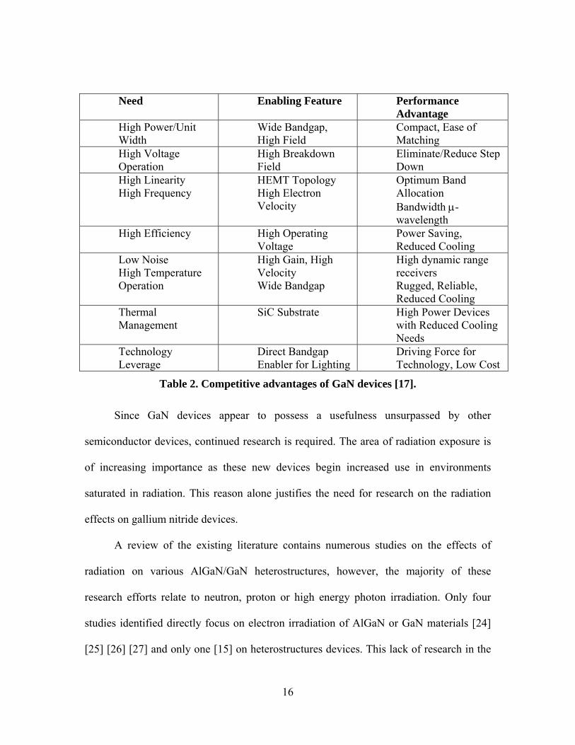
16
Need Enabling Feature Performance Advantage
High Power/Unit Width
Wide Bandgap, High Field
Compact, Ease of Matching
High Voltage Operation
High Breakdown Field
Eliminate/Reduce Step Down
High Linearity High Frequency
HEMT Topology High Electron Velocity
Optimum Band Allocation Bandwidth µ-wavelength
High Efficiency High Operating Voltage
Power Saving, Reduced Cooling
Low Noise High Temperature Operation
High Gain, High Velocity Wide Bandgap
High dynamic range receivers Rugged, Reliable, Reduced Cooling
Thermal Management
SiC Substrate High Power Devices with Reduced Cooling Needs
Technology Leverage
Direct Bandgap Enabler for Lighting
Driving Force for Technology, Low Cost
Table 2. Competitive advantages of GaN devices [17].
Since GaN devices appear to possess a usefulness unsurpassed by other
semiconductor devices, continued research is required. The area of radiation exposure is
of increasing importance as these new devices begin increased use in environments
saturated in radiation. This reason alone justifies the need for research on the radiation
effects on gallium nitride devices.
A review of the existing literature contains numerous studies on the effects of
radiation on various AlGaN/GaN heterostructures, however, the majority of these
research efforts relate to neutron, proton or high energy photon irradiation. Only four
studies identified directly focus on electron irradiation of AlGaN or GaN materials [24]
[25] [26] [27] and only one [15] on heterostructures devices. This lack of research in the

17
area of AlGaN / GaN heterostructures leaves little doubt as to the need for increased
research emphasis in the area of electron irradiation of AlGaN / GaN heterostructures.
Nevertheless, a review of the proton, neutron and limited electron studies provides a
wealth of information about radiation effects on AlGaN / GaN heterostructures.
Radiation Effects of Protons on AlGaN / GaN
Ionascut-Nedelcescu et al. accomplished an excellent study on the hardness of
Gallium Nitride [12]. They irradiated GaN diodes at room temperature with electrons of
various energies from 300 to 1400 keV. They report that three different experiments
determined that GaN resists damage more than gallium arsenide. In the first experiment
the bulk material was studied by photoluminescence. In the second case, the
electroluminescence from GaAs and GaN was compared. The third and final experiment
studied the resistivity of a two-dimensional electron gas. No displacement of nitrogen
atoms was observed, so they concluded that the nitrogen sublattice repairs itself by room
temperature annealing [12]. Perhaps the most significant result of their work was the
determination of the displacement energy of the gallium atoms in the GaN [12]. They
reported that a threshold energy of 440 keV corresponds to a displacement energy of
19 ± 2 eV for gallium [12].
An early study, in 1999, by Wilkins et al. [24] looked at ionization and
displacement damage irradiation in two-dimensional gas transistors. Their study used
monoenergetic 55 MeV protons up to a maximum fluence of 5 × 10 P
10P cmP
-2P in order to
simulate the expected proton environment in low earth orbit that might be experienced by
the International Space Station with a mission duration of 70-100 years. Apparently, the
gamma radiation reduced the transconductance of the device while the proton radiation

18
increased the transconductance. Later research concludes the opposite for proton
radiation; however, at the time they concluded that HEMTs were viable for use in space
due to this proton radiation induced enhancement.
Luo et al. [11] investigated the device specific effects of high-energy proton
irradiation on AlGaN / GaN high-electron mobility transistors (HEMTs). They used 40
MeV protons at fluences that replicated decades of exposure in low-earth orbit. The
results demonstrated a decrease in extrinsic transconductance, drain-source current
threshold voltage, and gate current. They concluded that the data indicated that protons
created deep electron traps that resulted in HEMT channel resistance. The room
temperature post irradiation annealing restored approximately 70% of the initial
transconductance and drain-source current.
Polyakov et al. [29] studied the effects of implantation with 150 keV protons on
samples of n-GaN in order to study the nature of point defects and device isolation. They
observed a degradation of minority carrier diffusion length. Deep level spectroscopy
measurements revealed deep electron traps with activation energies between 0.2 and 0.95
eV and deep hole traps with energies of between 0.25 and 0.9 eV. The results indicated
that the 0.75 eV electron traps and/or the 0.6 eV hole traps were probably responsible for
lifetime degradation. Excellent recovery of the electrical conductivity of the implanted
samples resulted after annealing at temperatures greater than 250°C.
Hu et al. [30] studied the degradation of AlGaN/AlN/GaN HEMTs due to 1.8 MeV
protons at fluences up to 3 × 10P
15P cmP
-2P. These devices possessed high radiation tolerance
up to 1 × 10P
14P cmP
-2P, but demonstrated a decreased sheet carrier mobility due to increased
carrier scattering and decreased sheet carrier density due to carrier removal at higher

19
fluences. Overall device degradation was noted to be a decrease in the maximum
transconductance, an increase in threshold voltage, and a decrease in the drain saturation
current as shown in Figure 4 below.
Figure 4. Transconductance versus gate-source voltage for AlGaN/AlN/GaN
HEMTs before and after 1.8 MeV proton irradiation with fluences from 1 × 10P
13
P cmP
-2P to 1 × 10 P
15P cm P
-2P [30].
Gaudreau et al. [14] investigated the effects of 2-MeV protons on the transport
properties of the two-dimensional electron gas at the AlGaN/GaN interface. In a fluence
range of 1 × 10P
13P to 7 × 10 P
15P cmP
-2P, the results of proton irradiation showed a carrier
density decrease of a factor of two while the mobility degraded by a factor of a thousand.
At a fluence between 3 × 10 P
14P and 3 × 10P
15P cmP
-2P the two dimensional gas changed phase
from a conductor to an insulator which the authors say could be used to establish an
upper threshold for radiation damage. They concluded that mobility changes are
dependent on the radiation and not sheet charge density. They stated that this indicates

20
that in a real two-dimensional gas system, if the performance of the system depends
mainly on mobility, then the system may function properly only until a critical fluence is
reached followed by abrupt failure at higher fluences. Additionally, the authors reconfirm
other research that indicated that AlGaN/GaN is at least two orders of magnitude more
radiation-resistant than AlGaAs/GaAs.
Figure 5. Common-source drain current as a function of gate voltage and
transconductance of the same transistor pre-irradiation (solid line), post-10P
12P cm P
-2P
fluence (dashed line), and post-5 × 10 P
13P cm P
-2P fluence (dotted line) [13].
In 2002, White et al. [13] examined the effects of 1.8 MeV proton irradiated
AlGaN/GaN MODFETs. The effects of proton irradiation on the electrical transfer
characteristics of the device include: a decrease in the saturation current, drain current
and transconductance as shown in Figure 5 [13]. White et al. believe that proton radiation
forms spatially localized changes in the electronic properties of the AlGaN/GaN
heterostructures that reduces the internal electric field as it forms charged defects. The
defects created reduce the charge density in the two-dimensional electron gas. This dual
reduction, electric field and 2DEG, causes the decrease in the saturation current, drain
current and transconductance [13].

Most recently, in 2004, Hu et al. [31] investigated the energy dependence of
proton-induced degradation in AlGaN/GaN HEMTs. They found that the devices
exhibited little degradation when irradiated with 15 MeV, 40 MeV and 105 MeV protons
at fluences up to 1013 cm-2 and the damage recovered after room temperature annealing.
Very little degradation was found for proton energies greater than 15 MeV. For a fluence
of 1013 cm-2 1.8 MeV protons, the drain current decreased by approximately 10% and the
maximum transconductance decreased by 6.1% [31]. These results are demonstrated
below in Figure 6 and Figure 7.
Figure 6. Transfer characteristics for AlGaN/GaN HEMTs before and after 1.8
MeV proton irradiation at various fluences [31].
21

Figure 7. Transfer characteristics for AlGaN/GaN HEMTs before and after 105-
MeV proton irradiation at different fluences [31].
Radiation Effects of Electrons in AlGaN / GaN
Fang et al. [26] studied deep centers in electron-irradiated n-GaN on sapphire. The
electron irradiation created VN (nitrogen vacancies) related centers with an activation
energy of 0.06 eV and a deeper center with ET = 0.85 eV. Their conclusion indicated that
point defects (vacancies and interstitials) in semiconductors are created by high-energy
electron irradiation [26].
Goodman, et al. [24] studied electron irradiation induced defects in n-GaN and
they found that electrons were extremely adept at introducing point defects. They used
deep level transient spectroscopy (DLTS) to investigate the electron trap defects during
high-energy electron irradiation. Their results indicate that the major electron induced
defect is not one defect level but is made up of at least three defect levels [24].
22

Coskun et al. [25] describe an experimental set-up for in situ Hall measurements
under high-energy electron irradiation for various wide band gap semiconductor
materials. They indicate that an associated cryostat allows irradiations to be carried out
over a range of temperatures from 95–-300 K. They do not report on specific results, but
merely describe the experimental set-up, thus providing useful guidance for follow-on
experimental set-ups of the same type [25].
Look et al. [32] in 1997 conducted an experiment with high-energy (0.7 to 1 MeV)
electron irradiation and GaN on sapphire. The result was the productions of shallow
donors as well as deep and shallow acceptors. Their data, coupled with theory, indicated
the shallow donor is an N vacancy and the acceptor is a rare appearance of an N
interstitial. Their total-energy calculations suggest that both VN and NI are not expected
to exist in large quantities in as-grown n-type material, but appear after irradiation.
In 2003, Look et al. [27] conducted electron irradiation experiments on Gallium
Nitride. They conducted their experiment at room temperature with 0.42 MeV electrons,
a current of 2 µA/cm2 and a total fluence of about 3.6 x 1017 cm-2. Look et al. base their
conclusions on the calculated threshold displacement energies (Ed) by Nord et al.
Accordingly, the minimum Ed for N displacement is 25 eV and for Ga is 22 eV. Look et
al. take into consideration an average acceptance angle of 15º to account for thermal
motions and possible beam misalignment in order to calculate N and Ga displacement
energies of 66 and 38 eV, respectively. From these calculations and factoring in the
higher mass of the Gallium, they conclude that the minimum electron energy required for
N displacement is 0.32 MeV and for Ga displacement is 0.53 MeV. They conclude that
the N production rate should be 0.03 cm-1 at the electron energy of 0.42 MeV and will
23

continuously exceed the Ga production rate up to at least 0.87 MeV. From these facts,
they deduced that this level of radiation produces N-sublattice displacements and only the
N vacancy is the shallow donor produced by 0.42 MeV electron irradiation [27].
Also in 2003, Sattler [21] showed that various AlGaN /GaN MODFETs were
radiation tolerant after receiving various total fluences up to 3.67×10¹⁵ e-/cm2.
Additionally, he demonstrated that there were no significant changes between room
temperature pre-irradiation and post-irradiation I-V measurements. He consistently
observed non-fluence dependent increases in both drain and gate current for two different
irradiations as shown in Figure 8 and Figure 9 below. He reported that these increases
annealed out at room temperatures. He explained that the gate leakage increases were due
to the enhancement of trap-assisted tunneling through the AlGaN layer caused by
radiation-induced trap creation in the AlGaN.
Figure 8. Sample A0409 FatFET First Irradiation: Change in I-V Curves at LiN Temperature (0.45 MeV Electrons) [21].
24

Figure 9. Sample A0409 FatFET Second Irradiation: Change in I-V Curves at LiN Temperature (0.45 MeV Electrons) [21].
Sattler [21] stated that the transistor changes are not related to the total fluence but
rather to the initial radiation exposure as shown in Figure 9.
Sattler [21] proposed that the drain current increase results from one of two
possibilities: (a) the current increase was caused by a direct increase in carrier
concentration in the 2DEG; (b) the 2DEG population remained unchanged and the
increase was caused by an increase in the electron mean velocity in the 2DEG. His
experiment did not record C-V measurements, but suggested that either one of the
choices can easily be proven over the other through fluence-dependent C-V
measurements and the calculation of the 2DEG carrier concentrations. Table 3 presents
the relevant irradiation information for the two FATFET samples that were not
25

completely destroyed during his experiment and provides a reference starting point for
subsequent irradiation levels in follow-on experiments.
Sample Energy (MeV)
Beam Current
(µA)*
Relative Fluence (e-/cm2)
Relative Irradiation Time (min)
Total Fluence (e-/cm2)
Total Irradiation Time (min)
A0408 0.45 0.13 1×10¹⁴ 7 1×10¹⁴ 7 A0408 0.45 0.13 2×10¹⁴ 13 3×10¹⁴ 20 A0408 0.45 0.13 6×10¹⁴ 39 9×10¹⁴ 59 A0409 0.45 0.3 3×10¹⁴ 8 3×10¹⁴ 8 A0409 0.45 0.3 6.7×10¹⁴ 13 9.7×10¹⁴ 21 A0409 0.45 0.3 9×10¹⁴ 18 1.87×10¹⁵ 39 A0409 0.45 0.3 1.8×10¹⁵ 50 3.67×10¹⁵ 89
Table 3. Experimental Device Irradiation Values as conducted by Sattler [21].
Capacitance-Voltage Measurements
N. Shaar et al. [33] in March 2004, used capacitance-voltage (C-V) measurements
to characterize MOS devices and discuss various measurement failures that resulted from
using this technique to characterize the devices. Additionally, they provided equations
and explanations for determining oxide capacitance (1), the minimum capacitance (2) and
the flat-band capacitance (3) as well as the flat-band voltage (4). An interesting
discussion and solution to hysteresis problems that resulted during measurement were
also provided. They suggested varying the voltage by sweeping from positive to negative
and then back to positive again to alleviate the hysteresis problems. Overall, this is an
excellent article stressing the foundational factors of capacitance-voltage measurements
[33]. The major equations (8), (9), and (11) used to calculate the minimum capacitance
and doping concentration from their research are described later in the theory section;
however, their experimental results showing the variation of capacitance measurements
through a range of gate voltages is plotted in Figure 10.
26

Figure 10. Typical plot of the variation of the capacitance (pF) of a 500 µm x 500 µm capacitor versus gate voltage (VG) ranging from –4.7 to +4.7 volts [33].
P. Notingher et al. [34] in the 2002 Annual Report Conference on Electrical
Insulation and Dielectric Phenomena characterized the electric charge in both non-
irradiated and irradiated MOS structures using C-V measurements. They offered a broad
explanation of the uses of capacitance-voltage measurements at high and low frequencies
in order to estimate the amount of trapped charge in the oxide layer, as well as detailed
explanations of the accumulation, depletion and inversion regions of a MOS capacitor
[34].
Tamotsu Hashizume et al. [35] used capacitance-voltage measurements to
characterize AlN/GaN MIS structures. The use of high frequency C-V measurements
clearly showed deep-depletion behavior at room temperature and allowed for the
derivation of the doping density from the slope of the 1/C2 plots. Additionally, they
determined the low value of interface state density Dit of 1×1011 cm-2 eV-1 around Ec –
27

0.8 eV position. The article also possesses excellent experimental examples of C-V plots
that reinforce the textbook C-V plots [35].
Figure 11. Typical C-V curve measured in darkness at room temperature [35]
Figure 12. 1/C2 characteristics as a function of bias voltage [35].
Ambacher et al. [36] conducted a study on the 2DEG induced by spontaneous and
piezoelectric polarization in AlGaN/GaN heterostructures using various methods, but
28

29
most notably a C-V profiling technique. They provide an equation (1) that enables the
researcher to obtain the carrier concentration from capacitance measurements [36].
dCdV
qC
VC oN εε
3=− , (1)
where V is the voltage applied across the gate, C is the measured differential capacitance
per unit area, and ε is the dielectric constant of the material, εBo B = 8.854 x 10P
-14P F cmP
-1P and
q is the charge on an electron [36]. Using this method on a sample of Al B0.24BGa B0.76 BN with a
thickness of 20 to 40 nm, they obtained carrier concentrations of 6×10P
12P to 9×10 P
12P cmP
-2PB. B
They report that the C-V carrier concentration (NBC-VB) is equal to the free carrier
concentration. Their sample dimensions are compatible with the dimensions of the
samples used in this research and are excellent for comparing calculation results using
equation (5) with data obtained from the FATFET [36].
Pavol Pisecny et al. [37] use the quasistatic C-V method to determine interface
trap density (DBitB) in MOS structures irradiated by 305 MeV Kr+ and 710 MeV Bi+ ions at
various fluences. This paper provides an excellent description of low frequency
measurements highlighting the main advantage of the low frequency C-V method in
determining the distribution of DBitB across the entire width of the bandgap. Paramount to
this research is their comment on the radiation changes as observed through C-V
measurements. They report that the radiation changes the DBitB and this change can be
observed through the slope of the C-V curves in the depletion and weak inversion
regions. Additionally, they report that the flat-band voltage shifts to a higher negative
value as the fluence increases. From their experimental data, they conclude that an
increase in fluence and ion mass induces an increase in DBitB. Their final conclusion is that

the irradiated MOS devices maintain the basic capacitance behavior even after high-
energy irradiation [37].
E. F. da Silva et al. [38] use high-frequency C-V measurements to study interface
defects in n-type MOS capacitors after X-ray irradiation. This paper provides
representative C-V curves before irradiation and after various levels of radiation. The
curves clearly show a parallel negative voltage shift indicating generation of positive
interface oxide charge. Although not specifically the same, the devices used in this
experiment produce similar plots and the curve by da Silva provides an example of a
possible result after irradiation. The interface traps stretch out the C-V curve as compared
to the pre-radiation plot [38] as shown in the example plot Figure 13.
Figure 13. High frequency capacitance-voltage curves for a n-type MOS capacitor measure: (a) before irradiation; (b) after 143 Mrad (Si) irradiation; and (c) after
482 Mrad (Si) irradiation [38].
30

B. J Gordon [39] provided textbook basics on C-V measurements in “C-V plotting:
myths and methods.” He provided solutions to common pitfalls and directions that make
conducting C-V measurements second nature. He detailed step-by-step instructions for
correct application of the voltage sweep direction as well as comprehensive descriptions
of the accumulation, depletion and inversion regions. Overall, this is an excellent source
for initiating C-V measurements.
As can clearly be seen, there are numerous studies on capacitance-voltage in
various types of MOS capacitors which function in a similar manner to HEMTs;
however, no specific reports could be found detailing C-V measurements on HEMTs.
Research Justification
Since gallium nitride devices are projected to play important roles in sensors and
satellite based systems where they might be subject to intense effects of radiation, it can
be concluded from a study of the current literature that continued study and experimental
procedures on the effects of radiation on AlGaN/GaN HEMTs is justified. The literature
is conspicuously absent of in-depth research concerning the irradiation of GaN
heterostructures especially with respect to capacitance-voltage measurements; therefore
this research investigated the effects of radiation on GaN heterostructures through
capacitance measurements.
31

III. Theory
CV Measurements
The capacitance-voltage (C-V) measurement technique conducted at frequencies
above 10 kHz is a widely used method for measuring the charge present in Metal Oxide
Semiconductor (MOS) devices. This technique allows for determining the amount of
charge held within the oxide layer making up the insulator portion of the device. In the
high frequency case, the modulation frequency is high enough that the minority carriers
are too slow to respond to the voltage modulation, whereas in the low-frequency case the
frequency applied is low enough that the minority carriers respond sufficiently to the
voltage modulation. The almost universally accepted high-frequency measurement is
1 MHz and is the frequency used in this experiment to obtain high-frequency
measurements needed to observe the inversion region.
The normalized textbook capacitance-voltage curve below clearly shows the
characteristic accumulation, depletion and inversion regions.
Figure 14. Textbook example of a Capacitance-Voltage Curve [38].
32

33
A typical MOS device is shown in the diagram below. The GaN and Al BxBGa B1-x BN
devices as shown in Figure 2 and used in this experiment are similar in structure to a
typical MOS device that functions like a parallel plate capacitor. The device structure
depicted below can be treated as a series of two capacitors: the capacitance of the oxide
material (SiO B2 B) and the capacitance of the silicon (Si).
Figure 15. Diagram of a typical MOS structure [34].
The capacitance of the oxide is independent of any applied gate voltage and is
found by
ox
oxod
AOXC εε= , (2)
where ε Bo B is the permittivity of free space, ε BoxB is the dielectric constant of the oxide, A is
the surface area of the gate and dBoxB is the thickness of the oxide layer [34]. A space
charge (W) layer is formed in the depletion region when a gate bias (VBGB) is applied which
allows the Si layer capacitance to be determined as discussed in following paragraphs.
The C-V measurement method obtains measurements of capacitance by applying a
high or low frequency sinusoidal voltage of a few millivolts superimposed over the bias
voltage. In this way, the capacitance is measured for various values of the bias voltage,

VG or gate voltage. The Keithley 590 C-V Analyzer used in this experiment uses this
method to measure the capacitance. A theoretical output plot from a n-type MOS
capacitor and the n-type device used in this experiment is shown in the figure below.
Figure 16. Shape of Capacitance-Voltage curves for ideal and real MOS capacitors with n-type Si substrate [34].
There are three modes of operation for a MOS device: accumulation, depletion,
and inversion. Each of these will be discussed in detail below.
For an ideal n-type HEMT, just like an ideal MOS, accumulation occurs when a
positive gate bias (VG > 0) is applied and the positive charge of the gate attracts electrons
(majority carriers) from the substrate, thus accumulating these majority carriers. The GaN
behaves as a conductor and its capacitance is very high with respect to the AlGaN
capacitance and therefore the overall capacitance is equal to the capacitance in the
AlGaN [34].
34

35
AlGaNdevice CC = (3)
As stated above, the CBdevice B is similar to CBoxB and is therefore equal to:
AlGaN
AlGaNod
AdeviceC εε= . (4)
When a large positive voltage (VBGB > 0) is applied to the gate, strong accumulation
is obtained and an extremely high density of majority carriers stacks up at the GaN
surface (Figure 17a). These electrons effectively block the interior of the GaN from
changes in the electric field due to the effects of the gate voltage modulation by the
applied frequency. At this point, since there is no depletion layer (W) in the GaN all of
the field lines terminate at the surface of the GaN and the GaN acts to short circuit the
AC signal. Thus, in accumulation the overall device behaves like a parallel-plate
capacitor with the AlGaN acting like the dielectric spacer and the equivalent of an ‘oxide
capacitance’, CBAlGaN B. This corresponds to the maximum capacitance of the device [34].
When a negative bias is applied (VBGB < 0), the negative charge on the gate pushes
the electrons of the GaN away (Figure 17b). A positive charge builds up in the device due
to the depletion of the semiconductor originating at the GaN-AlGaN interface. The
depletion layer width continues to increase as the gate voltage decreases. The capacitance
of the device drops as VBGB decreases and is then [34]:
WAlGaNdevice CCC111 += . (5)
Finally, as the potential across the device continues to decrease further (VBGB << 0),
another charge emerges at the AlGaN/GaN interface due to an accumulation of minority
carriers (holes). This accumulation of holes forms an inversion layer (Figure 17c). As the
gate voltage continues to decrease, the depletion width hardly increases any more since

36
the charge due to the holes increases as the gate voltage increases. The depletion width,
W, reaches a maximum in this mode and as a result the capacitance is a minimum. This
value is then [34]:
Max
GaNoW
AMinC εε= (6)
Or alternatively written,
SCOX
SCOX
CCCC
MinC += or GaNAlGaN
GaNAlGaN
CCCC
MinC += (7)
Where CBSC B is the capacitance of the semiconductor.
A real device behaves somewhat differently due to fixed and mobile charges in the
AlGaN layer and charge in surface states. The result of these additional charges is a
stretching of the characteristics or a shift either to the right or left along the VBGB axis as in
Figure 25.
A fixed charge in the ‘oxide’ layer shifts the measured curve along the VBGB axis. A
positive fixed charge at the interface between the AlGaN and GaN shifts the flat-band
voltage by an amount that is equal to the charge divided by the oxide capacitance.
OX
FCCQ
FBV =∆ (8)
This shift changes linearly as the position of the fixed charge varies from the gate
in the oxide. The shift is a maximum when the fixed charge is located at the AlGaN /
GaN interface and zero when the fixed charge is located at the gate contact and AlGaN
interface [33].
A mobile charge also causes a flat-band voltage shift to occur and is also described
by equation (8) the same as that for a fixed charge. The fixed charge and the mobile
charge measured curves will differ since a positive gate voltage causes mobile charges to

37
move away from the gate, whereas a negative gate voltage will attract the mobile charges
toward the gate. An excellent method for recognizing the mobile charge is through the
hysteresis in the high frequency capacitance curve after sweeping the gate voltage
forward and backward. This will be explained in a later next section.
From the inversion region, the minimum capacitance is found and can be used to
calculate the doping concentration of the GaN using the following equations [33]:
( ) 11
41
−−
⎥⎦⎤
⎢⎣⎡ += φ
εε DGaNo
AlGan
NqCMinC (9)
where, ( )i
Dn
Nq
kT ln=φ , and also by use of equation (1) [36],
dCdV
qC
VC oN εε
3=− . (10)
Similarly, once the doping concentration is found, the flat-band capacitance can be
determined using [33]:
[ ] 11
−+=
DGaNoAlGan NqkT
CFBC εε . (11)
Additionally, the depletion depth can be determined as well from the capacitance:
CAW d
ε= . (12)
The previous discussion related to a metal-oxide semiconductor, which is assumed
to possess similar capacitance characteristics as a heterostructure. However, the actual
energy bands for a heterostructure are not the same as those of a MOS device as depicted
in Figure 17. These differences are discussed next.

Figure 17. Band bending diagrams for a Metal Oxide Semiconductor under various applied biases a) accumulation, b) depletion, c) inversion [40].
38
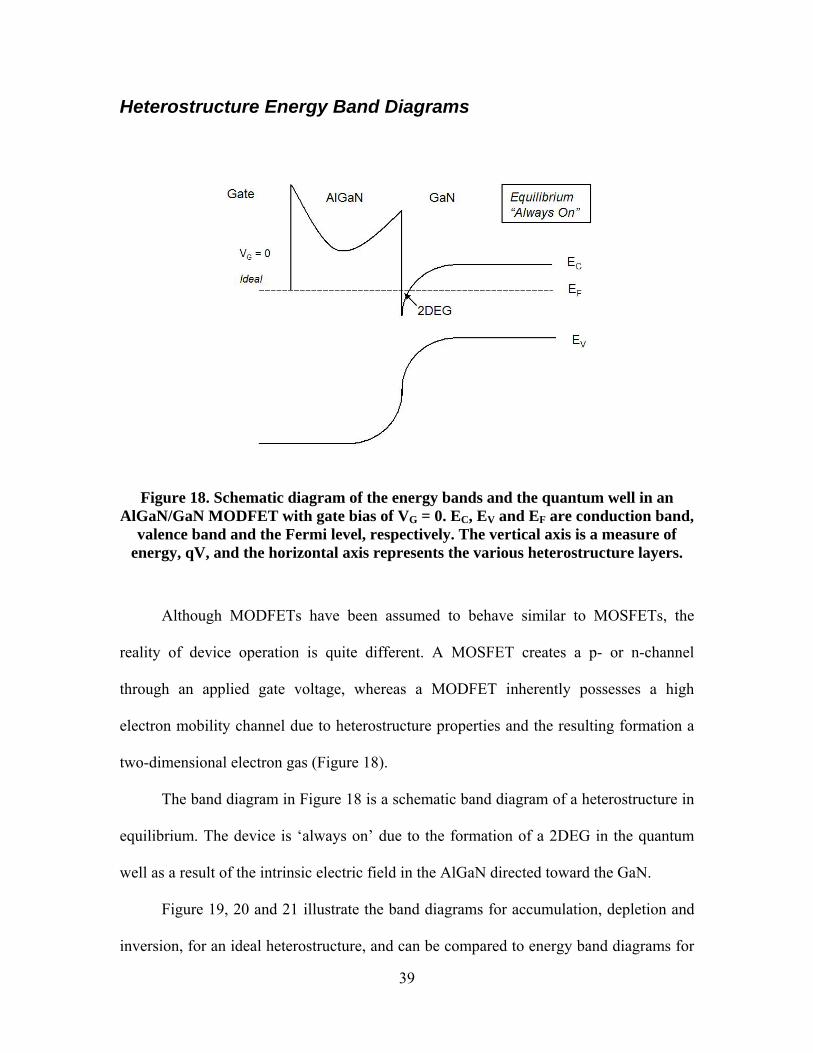
Heterostructure Energy Band Diagrams
Figure 18. Schematic diagram of the energy bands and the quantum well in an AlGaN/GaN MODFET with gate bias of VG = 0. EC, EV and EF are conduction band,
valence band and the Fermi level, respectively. The vertical axis is a measure of energy, qV, and the horizontal axis represents the various heterostructure layers.
Although MODFETs have been assumed to behave similar to MOSFETs, the
reality of device operation is quite different. A MOSFET creates a p- or n-channel
through an applied gate voltage, whereas a MODFET inherently possesses a high
electron mobility channel due to heterostructure properties and the resulting formation a
two-dimensional electron gas (Figure 18).
The band diagram in Figure 18 is a schematic band diagram of a heterostructure in
equilibrium. The device is ‘always on’ due to the formation of a 2DEG in the quantum
well as a result of the intrinsic electric field in the AlGaN directed toward the GaN.
Figure 19, 20 and 21 illustrate the band diagrams for accumulation, depletion and
inversion, for an ideal heterostructure, and can be compared to energy band diagrams for
39

an n-type MOS device in Figure 17. In the accumulation region, an applied gate voltage
greater than zero draws charge carriers from the GaN and populates the 2DEG. The
conduction band drops below the Fermi level and creates a triangular quantum well
containing the 2DEG. For an ideal MODFET, an applied bias of VG = 0 indicates that the
device is in equilibrium and always on due to the 2DEG. In depletion, the applied gate
voltage is less than zero that has the effect of decreasing the 2DEG in the quantum well.
Essentially, an applied bias less than zero starts to turn the device off by collapsing the
well. The larger the negative applied bias, the more the well collapses as the Fermi level
drops toward the valence band. When the conduction band just touches the Fermi level,
the device has attained maximum depletion. As the applied gate bias continues to become
increasingly negative, the Fermi level continues to drop away from the conduction band
and the device enters inversion. The gate bias where this occurs is the threshold voltage.
Figure 19. Band diagram of AlGaN/GaN MODFET in accumulation due to an applied gate bias of VG > 0.
40

Figure 20. Band diagram of AlGaN/GaN MODFET in depletion due to an applied gate bias of VG < 0.
Figure 21. Band diagram of AlGaN/GaN MODFET in inversion due to an applied
gate bias of VG << 0.
41

Performing CV Measurements
In order to obtain accurate CV measurements, the measurements must be taken
ensuring that the data is only recorded at equilibrium conditions and that the signals are
measured in the correct sequence in order to compensate for stray capacitance. The
Keithley Model 590 provides an integral setting that compensates for stray capacitance.
A method used to verify that the measurement equipment records true capacitance
is by using calibration capacitors. These are precisely known capacitance sources that are
connected to the CV analyzer in place of a test device. Specifically, the known
capacitances used in this experiment were two Keithley devices of 479.08 pF and 1815.1
pF at 1 MHz and 22.3 °C (part number 5900-301-7 and 5900-301-8, respectively.) The
capacitance measurements of the experimental setup in Figure 32 were accurately
verified using the calibration capacitors and found to be within 1-3% of the known value.
The most important measurement requirement is the recording of data under
equilibrium conditions. Each voltage step must allow the ‘capacitor’ to become fully
charged before a measurement is taken. This fully charged condition is known as the
equilibrium condition. The way in which the Keithley 590 accomplishes this is after
initially applying the voltage there is a hold time before measuring the capacitance and
after each subsequent voltage step there is a delay before recording the next capacitance.
This hold and delay helps eliminate hysteresis curves for capacitance measurements
taken in different directions (i.e. from -8V to 0V or from 0V to -8V). For this experiment,
the Keithley 590 CV analyzer measurements produced negligible hysteresis curves as
shown in Figure 22. The blue data points show the measurements taken from -8 V to 0 V
42

while the purple data points show measurements taken from 0 V to -8 V with no
noticeable deviation.
Hysteresis
0.002.004.006.008.00
10.0012.0014.0016.0018.0020.00
-8 -7 -6 -5 -4 -3 -2 -1 0
Gate Voltage [V]
Cap
acita
nce
[pF]
-8 V to 0 V0 V to -8 V
Figure 22. Plot showing the sweep direction (start voltage of –8V (solid square) and
0V (open square)) and the statistically insignificant effects of hysteresis on the measurements.
The preferred measurement sequence is from the inversion to accumulation since it
is faster and more controllable that sweeping from accumulation to inversion. In this
experiment, all subsequent measurements were taken from inversion to accumulation
through an applied gate voltage range of -6 V to 0.5 V. This measurement technique is in
accordance with the procedures as outlined in [39] except that the experimental setup did
not incorporate a light in the beam tube to stimulate carriers in the device. Step two was
not performed. Figure 23 is characteristic of the n-type devices used in this research.
43

Figure 23. Illustration of the standard C-V measurement procedures: (1) Apply Bias, (2) Light On, (3) Light Off Stabilization, (4) Bias Sweep [39].
Additionally, before any measurement sweeps start and prior to recording data, all
lights should be turned off in order to take all measurements in total darkness since the
GaN heterostructures under investigation are extremely light sensitive. For this
experiment, this was only a consideration during bench testing measurements and not
during the irradiation process when the transistors were in the beam tube of the Van de
Graaff machine.
Radiation Interaction in GaN
There are two principal effects of ionizing radiation on Gallium Nitride. These two
effects are the introduction of permanent and transient defects in the material. Permanent
are the defects of total dose and transient defects are dependent upon the dose rate. With
44

45
respect to the AlGaN / GaN HEMTs both of these play a role in transistor operation
following irradiation and have an equal chance of occurring simultaneously [18].
The permanent defects manifest themselves as displacement damage as a result of
elastic collisions with the lattice atoms as well as populate or depopulate traps. The rate
of displacement damage is a function of the atomic binding energy and the energy
transfer due to the collision [18]. In the wurtzite crystal structure of GaN, the nitrogen
atoms (N) are bound much more tightly than the gallium atoms (Ga); however, the mass
of the gallium is five times as massive as the nitrogen atom. The energy deposited by an
elastic collision is extremely dependent upon the atom’s mass, which means much more
energy is transferred to the atom with the least mass.
As stated by Greene [18], Nord et al. has previously calculated the various
displacement energies for the atoms in gallium nitride. The minimum energy required to
displace a gallium atom from the lattice is 22 ± 1eV while the minimum energy needed to
displace a nitrogen atom from the lattice is 25 ± 1eV. This minimum is calculated over all
angles, while the average energy required for displacement from the lattice is 45 ± 1eV
and 109 ± 2eV for Ga and N, respectively. On the other hand, the maximum amount of
energy that can be transferred to an atom through coulomb scattering by an energetic
electron is
( )
−
−− += ecm
cmEtrans EE
atom
ee2
22max 2 (13)
The table below shows the maximum energy available to lattice atoms due to
irradiation by electrons of various energies as used in this research. These have been
calculated using equation 13.

Incident Electron Energy (MeV)
Maximum Energy Transferred to Nitrogen
Atom (eV)
Maximum Energy Transferred to Ga Atom
(eV) 0.45 20.27 100.86 0.7 36.87 183.45 0.8 44.58 221.45 1.2 81.53 405.73
Table 4. Maximum electron energy transferred to lattice atoms [18].
Using Table 4 above and Figure 24 below, nitrogen point defects will occur above
incoming electron energies of 0.3 MeV while gallium point defects start appearing
around electron energies in excess of 0.5 MeV. Once incoming electron energy reaches 1
MeV both defects will occur in the sublattice [18]. Additionally, according to Green, the
expected types of radiation-induced damage will most likely be VN, IN and related VGA
and IGA [36]. The above data is corroborated by the work of Look et al. with 0.42 MeV
electrons and the conclusion that the minimum displacement energy for nitrogen is 0.32
MeV and for gallium is 0.53 MeV [27].
Figure 24. Maximum energy transfer for gallium and nitrogen as a function of the incident energy. The average and minimum displacement energy for both gallium
and nitrogen are shown as horizontal lines [18].
46

Expected Radiation Effects on C-V Curves
The current literature provides minimal information on the radiation effects on the
capacitance measurements of GaN heterostructures. However, there is ample research
documenting the radiation effects on the capacitance characteristics of MOS devices. In
order to proceed in this research effort, GaN heterostructures and MOS devices are
assumed to possess similar capacitance characteristics. The discussion that follows relates
the characteristics of MOS devices to GaN heterostructures.
Radiation changes interface trap density, Dit, that can be observed on the slope of
C-V curves in depletion and weak inversion region. Also, the flat-band voltage VFB shifts
to a higher negative value with increasing fluence. An increase in fluence creates a
growth of Dit. Nevertheless, irradiated MOS structures retain their basic capacitance
behavior even after high-energy radiation [30] as shown the high frequency capacitance-
voltage curve of Figure 13 [38].
Numerous experimental results indicate that interface traps build up over time
during irradiation in Silicon MOS devices, but more experimental results are required
before this can be conclusively stated for GaN. This incremental build up can occur in a
few seconds to thousands of seconds at room temperature. Figure 25 below illustrates the
time dependent build up of interface traps through normalized high-frequency C-V
curves of a MOS capacitor before irradiation and at various time intervals from 0.04
seconds to 400 seconds after irradiation [3].
47

Figure 25. Normalized 1-MHz CHF-V curves of an MOS capacitor at several times following pulsed electron beam irradiation [3].
There is no change in shape to the curve immediately following irradiation at 0.04
seconds. The curve is simply shifted in the negative direction along the applied voltage
axis. From 0.4 seconds to 4 seconds the curves show a shift back in the positive direction
with only slight changes in shape. This return toward the positive direction is due to the
annealing of trapped holes in the insulator. Of interest, between 4 seconds and 40 seconds
the curves begin to stretch along the applied voltage axis. This stretching increases at the
400 seconds mark with a noticeable slope change. The changing slope over time is due to
the delayed build up of radiation-induced interface traps [3].
Figure 26 shows the doping dependence of a MOS-capacitor measured at high
frequency resulting in the measured C-V curves. In the case of an n-type device, the
effect of increasing the doping concentration from 1014 cm-3 to 1016 cm-3 is a vertical shift
in the capacitance in the inversion region of the curve. This shift occurs due to an
increase in charge carriers due to an increase in donors that increases the charge in the
48
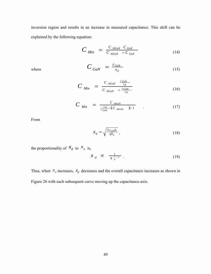
49
inversion region and results in an increase in measured capacitance. This shift can be
explained by the following equation:
GaNAlGaN
GaNAlGaN
CCCC
MinC += (14)
where d
GaNxGaNC ε= (15)
dx
GaNAlGaN
dxGaN
AlGaN
C
CMinC ε
ε
+= (16)
( ) 1+=
AlGaNGaNdx
AlGaN
CC
MinCε
. (17)
From
d
sGaNqNdx φε2= , (18)
the proportionality of dx to dN is,
2/11dNdx ∝ . (19)
Thus, when dN increases, dx decreases and the overall capacitance increases as shown in
Figure 26 with each subsequent curve moving up the capacitance-axis.

50
Figure 26. Doping dependence of MOS-capacitor high frequency C-V characteristics [41].
The expectation in any experimental results is that when this same vertical shift is
observed after irradiation by means of a comparison of the before and after irradiation
curves, then the electron irradiation will have caused an increase in the donor
concentration in the GaN. This increase will likely be due to displacement damage in the
GaN resulting in an active Nitrogen vacancy that is a donor. This influx of extra electrons
should be the cause of the increase in drain current as reported by Sattler [21] due to an
increase in the sheet charge density of the 2DEG.
The drain current model proposed by Morkoç et al. yields an equation for the
source-to-drain current which clearly shows the dependence of the IDS current on four
variables [42].
)()( xnxqWvI sDS −= (20)

51
where q is the charge on an electron, W is the gate width, v(x) is the electron mean
velocity and nBs B(x) is the carrier concentration. Both the charge of an electron and the gate
width are constants which means that any change in the drain current is caused by either a
change in the 2DEG carrier concentration or a change in the electron mean velocity in the
channel. C-V measurements cannot determine the electron mean velocity, but they can
and will be used to calculate carrier concentration.
Ambacher et al. [36] use equation (21) and the capacitance from the C-V profiling
technique to yield the carrier concentration in the inversion region. The sample
parameters used by Ambacher et al. are close to the parameters of the samples used in
this research and calculations using equation (21) yield similar carrier concentrations for
data obtained on FATFETs used in this report when compared with Ambacher et al.
dCdV
qC
VC oN εε
3=− (21)
Equation (21) will be used in conjunction with the post-irradiation results similar
to Figure 26 to determine mathematically, as well as graphically, whether the carrier
concentration increases or decreases due to electron irradiation; thus, satisfying the
condition of the thesis hypothesis. These calculations are included in Appendix C.

IV. Experimental Procedures
Transistor Background
The GaN heterostructures used in this research are from wafer sections
manufactured by Cree using the metal-organic vapor-phase epitaxy (MOVPE) process
with a substrate of SiC layered with GaN and AlxGa1-xN. The transistor dimensions are
shown in Figure 30 and are as follows: the substrate is 413 µm thick; the GaN layer over
the substrate is a nominal thickness of 2 µm while the AlxGa1-xN layer over the GaN is 25
nm. The AlxGa1-xN is composed of a 27% mole fraction of AlN and 73% mole fraction of
GaN that results in a layer of AlxGa1-xN that is Al0.27Ga0.73N. According to the
specifications provided by Cree the room temperature carrier concentration is 1.3×10¹³
cm-2 while the mobility is measured as1300 cm2/V·s
The actual fabrication of the transistor was accomplished at the Air Force Research
Laboratories (AFRL) Sensors Directorate Aerospace Components and Subsystems
Technology Electron Devices Branch (SNDD). Sattler [21] provides an in-depth
description of the original fabrication, dicing and packaging process in a previous work.
Sattler’s previous research utilized all previously fabricated, diced and packaged devices.
In order to replicate the conditions of previous work as closely as possible, new devices
were diced and packaged from the remaining portions of the previously used wafer.
Although there are three wafer sections (JSO1A, JSO1B, and JSO1C) remaining from the
original disk manufactured by Cree only transistors from Wafer JSO1A were used in this
research. Wafer JSO1A consisted of approximately 40 chips containing transistors of
various types and is shown Figure 27 prior to dicing and packaging.
52

Figure 27. Wafer section JSO1A containing approximately 40 individual chips. Scale to the right is inches for comparison only.
The transistor used in this research is located in the upper right corner of the chip
and is called a FATFET to differentiate it from the other ‘thin’ transistors on the chip in
Figure 28. The name FATFET has gained acceptance due to the fact that the transistor
gate is 50 µm in length, which is much larger than a gate length of approximately 1.2 µm
for all other transistors on the chip. Figure 28 shows the location of the FATFET on the
chip as well as the contact connections labeled G, S, and D for gate, source and drain,
respectively. Figure 29 shows the special orientation of the gate, source and drain
contacts on the device. The vertical line AB corresponds to the cross section diagram in
Figure 30 that emphasizes the layered structure and composition of the device.
53

Figure 28. Close-up of individual chip showing FATFET location in upper left of the image to the right of the CV ring. Contacts labeled G, S and D. Photo taken by
Larry Callaghan of AFRL/SN.
Figure 29. Individual FATFET spatial layout.
54

Figure 30. Cross section of FATFET along AB in Figure 13.
Once the desired wafer was chosen for use in the experiment, Mr. Larry Callaghan
of AFRL/SN was employed to dice and package all of the chips on JSO1A. He
accomplished this feat within two days and produced 40 diced and packaged devices like
the one in Figure 31. This packaging process involved bonding the chip to the package
and then wire bonding the FATFET to the package pins. In this case, the first three pins
were used to attach the gate, source and drain from left to right Figure 28. The package
was left open to allow the electron radiation clear access to the transistors so that
attenuation of electrons by the package was not a factor.
55

Figure 31. Diced and packaged chip from wafer section JSO1A. Photo taken by Larry Callaghan of AFRL/SN.
Pre-Irradiation Characterization
After packaging was completed, the transistors were tested using two different
methods. One method used two Keithley 237 High Voltage Source Measurement Units
(SMUs) in order to obtain the I-V characteristics. These measurements determined the
transistor action and the gate leakage in order to choose transistors that possessed similar
operating parameters with respect to current output and leakage current. Another method
used a Keithley 590 CV Analyzer in order to obtain the capacitance and conductance data
to produce CV curves. Both methods utilized a National Instruments General Purpose
Interface Bus (GPIB), and a laptop running either an IV characteristics Microsoft Visual
56

Basic program [21] or a CV characteristics Microsoft Visual Basic program depending on
the measurements required (Appendix A – Visual Basic Data Acquisition Program).
Figure 32. Building 470 laboratory Experimental Setup for Pre-Irradiation C-V Characterization
Following the initial tests, the devices were retested using the experimental setup
that would be used to execute the irradiation experiment. The only addition to the
apparatus used was a cold head sample mount assembly as shown in Figure 33 that was
machined for previous work [21] by the AFIT model shop. The cold head is required in
this experiment for several reasons: 1) it maintains the devices at low temperatures
(~80K) during irradiation thereby ‘freezing in’ any defects created during irradiation, and
2) it allows electrical operation and measurement of samples following irradiation
without removing the sample from vacuum and low temperature, as well as concurrent
temperature monitoring using a Resistive Temperature Device (RTD) implanted in the
57

cold head. In the first method the transistor I-V curves were measured in a range of
0 V < VD < 10 V with gate voltages of VG = 0, -1 V, -2 V, -3 V, and -4 V; the sample was
always grounded during measurement. An important point is that the range of gate
voltages over which these transistors can operate is approximately -6 V < VG < 0.5 V. For
VG < -6 V the transistors enter cutoff (no 2DEG exists) and for VG > 0.5 V the transistors
cease to function properly causing the associated I-V curves to experience large
distortions [21].
All devices were initially tested at room temperature and then at ~80K for both the
I-V characteristics and the C-V characteristics. The plot in Figure 34 provides a
comparison of the C-V curves at room temperature (~22 C) and ~80K. Each curve in
Figure 34 is the average of 7 measurements of all nine-device averages that are
themselves averages of 7 measurements for each device. The pre-characterization curves
for room temperature and 80K for the devices used in this research are located in
Appendix B.
58

Figure 33. Cold Head and Sample Mounting Assembly [18].
CV Comparison of Average Room Temp and 80 K
0
2E-12
4E-12
6E-12
8E-12
1E-11
1.2E-11
1.4E-11
1.6E-11
1.8E-11
2E-11
-6 -5 -4 -3 -2 -1 0 1
Gate Voltage [Vg]
Cap
acita
nce
[F]
Room Temperature80 K
Figure 34. Comparison of capacitance-voltage measurements for nine devices averaged over seven cycles and measured at 300K and 80K.
59

Once the initial pre-characterizations were complete, the devices were mounted
on the cold head and tested to determine any additional capacitance induced by the cold
head and the feed-through wires. As expected, the wires and the cold head added to the
overall capacitance measured by the CV analyzer. A test device, A0411, similar to those
used in the irradiation experiments was used to determine this additional capacitance.
Three distinct tests were run: 1) measurement of the device alone, not attached to the cold
head but grounded, 2) measurement attached to the cold head ungrounded and 3)
measurement attached to the cold head and grounded. Figure 35 indicates the
comparative capacitances of the three different measurement systems. Due to the extra
capacitance inherent in the cold head and wires, it was imperative that during the
experiment the devices were characterized at low temperature (~80K) while the cold head
was attached to the beam tube of the VDG just prior to irradiation. This added additional
time to the measurements; however, this ensured that the base line measurements
reflected any additional capacitance due to the measurement system materials. For device
A0411, the additional capacitance at room temperature was an average of 6.63615×10⁻¹³
Farads which is 10% of a picofarad measurement and not negligible.
60

Test Device A0411 Grounded vs. Ungrounded Cold Head
0
2
4
6
8
10
12
14
16
18
20
-6 -5 -4 -3 -2 -1 0 1
Gate Voltage [V]
Cap
acita
nce
[pF]
Ungrounded Cold Head
Grounded Cold Head
Grounded Off Cold
Figure 35. Graphical representation of the impact of grounding the devices and the intrinsic (additional) capacitance added by the cold head mounting system.
Irradiation Experiments
Irradiation experiments were conducted at Wright State University under the
equipment supervision of Dr. Gary Farlow who operated the electron Van de Graaff
electron accelerator (Figure 36).
The Wright State University Van De Graaff generator produces low- to mid-
energy electrons in a range from 400 keV to about 1.8 MeV with beam currents at and
below 30 µA. The aperture area of the electron beam is 3.3 cm2 and this beam passes
through an aluminum tube that must be evacuated to at least as 9 x 10⁻⁶ torr. Within this
tube a relatively uniform beam of energetic electrons can be created. From specifications
provided in previous work, the temporal current deviation is estimated at ±3%, while the
temporal energy deviation is estimated at ±5% [21]. Additionally, Dr. Farlow estimates
61

that the spatial beam uniformity is ±2-3% as noted on a piece of irradiated plastic with a
2 cm by 2 cm discolored square etched by the electron beam [21]. The beam current was
used to control the fluence rate and was set between a range of 0.13 µA and 6.0 µA. The
total fluence is determined using a current integrator that measures the beam current
imparted onto the cold head. The most important component of the machine is the
cryogenically cooled vacuum cap at the end of the evacuated aluminum tube that holds
the device mounting assembly and electrical connections for temperature and electrical
measurements. Henceforth, this cap will simply be referred to as the cold head. Due to
added impressed currents from the electron beam causing transistor burnout in the
affected regions, true in-situ measurements could not be performed; however, all
experimental measurements were conducted at low temperature (~80K) under as low a
vacuum as possible within equipment capabilities. Ultimately, this was on average about
5 x 10⁻⁶ torr.
Figure 36. Van de Graaff facility at Wright State University.
62

Due to the operating parameters of the Van de Graaff generator, the energy range
of electrons used in this experiment was 0.45 MeV to 0.85 MeV and a fluence range of
1012 e-/cm2 to 1015 e-/cm2 based on beam current. This, however, fits in well with the
initial premise that these devices, as components of satellites, could experience an
electron fluence up to 3×10⁶ e-/cm2/min or an annual fluence of 9.46×10¹³ e-/cm2 while
on earth orbit.
The first irradiation experiment was conducted on the 12th of January 2005 due to
more than 10 weeks of maintenance on the VDG.
Figure 37. Sample device attached to cold head by clamp and contact leads soldiered to cold head feed-through lines.
All experiments began by mounting the device to the cold head, attaching the cold
head to the aluminum beam tube on the VDG and lowering the temperature of the device
63

64
with liquid nitrogen. The sample was mounted to the cold head by clamping the five
unattached contacts on the device as shown in Figure 37. The extraneous leads were
clamped to the cold head to ensure that a secure conductive path for any beam-deposited
charge could escape by way of the VDG current integrator, and thus reduce the chance of
device damage due to charge buildup. Additionally, the device was centered on the face
of the cold head to ensure that a uniform electron beam interacted with the transistor (The
electron beam is scanned to ⅓ intensity). Conductive grease was used to ensure a good
thermal connection with the cold head to assist in maintaining the device at a low
temperature. The grease also served as an electrical insulator between the cold head and
the metal packaging, nevertheless, this insulating effect is somewhat reduced at low
temperature and exposure to the electron radiation.
After the physical mounting of the device was accomplished, the three leads (gate,
source and drain) were soldered to the electrical feed-through lines on the cold head. The
gate was attached to one line while the source and drain were attached together to another
as in Figure 38. Once the device was cooled to ~80K, the sample was pre-characterized
while attached to the VDG in order to establish a pre-irradiation baseline. During the
measurement phase of the experiment, the Keithley 590 CV Analyzer was wheeled in on
a cart and positioned approximately ½ m from the cold head in order to reduce the chance
of measuring extraneous capacitance inherent in long cables.

Figure 38. Schematic of the Experimental Setup at the Wright State University Van de Graaff Facility
A major concern resulting from condensation on the electrical connections was the
possibility of an electrical short occurring between the numerous electrical lines on the
cold head. Isolating the lines by sealing them with paper towel strips and masking tape
kept this from occurring. This ultimately was not a problem as the water condensed onto
the tape and paper towels as shown in Figure 39.
65

Figure 39. Insulation of cold head by sealing with masking tape and paper towels. 1a) Cold head, 1b) Feed through lines, 2) Liquid nitrogen exit port, 3) Liquid
nitrogen input, and 4) VDG beam tube.
A time consuming portion of the procedure was the evacuation of the beam tube.
Prior to the irradiation of a sample, the beam tube was reduced to a vacuum level of at
least 9×10⁻⁶ torr. Once the beam tube was evacuated and the temperature lowered to
around 80K, the pre-irradiation baseline measurements were made. Due to lessons
learned from previous research [21], actual in-situ measurements were not attempted as
these measurements resulted in the destruction of samples. Rather, the following
procedure was used. The device was turned off and grounded completely to the cold head
and current integrator of the VDG. After the low temperature irradiation at the specified
66

electron energy and fluence, the VDG was turned off and the measurement apparatus was
moved into the irradiation room, connected to the leads of the cold head and powered up.
Prior to recording any measurements, the current integrator was disconnected and the
cold head ground was connected to the ground on the Keithley 590 in order to provide a
sufficient current path for any excess electrons deposited by the beam onto the cold head.
The initial irradiation plan called for using a sample to test the experimental setup
and record data using electrons with an energy of 0.45 MeV at an initial fluence of
1.0×10¹⁴ e-/cm2. However, due to an initial calculation error identified at the start of the
second day of irradiation all initial irradiations were with 3.3 times as many electrons as
initially desired. This error helps explain some of the observed results of A19.
After irradiating the first sample A19 to an actual total fluence of 3.3×10¹⁴ e-/cm2,
A19-1, while the device was left in the off mode (the coax lines running to the Keithley
590 were left connected but the 590 was turned off), the VDG was turned off and the
current integrator disconnected from the cold head metal. The cold head metal was then
shorted to the Keithley system ground and CV measurements were taken. Upon
examining the CV data, the device did not function according to design parameters. Due
to the recent maintenance on the VDG, the current output of the device was higher than
anticipated at about 100 µA or a current density of 6.024 µA/ cm2 when only 1 µA or a
current density of 0.06024 µA/ cm2 was desired. The extreme current load damaged the
device and resulted in the Keithley 590 measuring 9.9×1030 F during three attempts to
obtain usable capacitance data. Even after warming the cold head to room temperature
and disconnecting the cold head from the beam tube, capacitance measurements of A19
67

resulted in unusable data and an uncharacteristic CV curve. At this point, the cold head
was removed, and another device, A16, mounted.
The experiment continued with device A16 using the same procedure mentioned in
the previous paragraph. After irradiating the next sample to a fluence of 3.3×10¹⁴ e-/cm2,
A16-1, while the device was left in the off mode, the VDG was turned off and the current
integrator disconnected from the cold head. The cold head ground was then shorted to the
Keithley system ground and CV measurements were taken. Initially during a portion of
the first measurement cycle, the Keithley measured a capacitance of 9.9×1030 F and then
began recording capacitance values in the picofarad range. At this point, seven cycles
were recorded at the fluence rate of 3.3×10¹⁴ e-/cm2. The experiment continued by
disconnecting the measurement equipment, turning the VDG on, and irradiating the
sample to 6.6×10¹⁴ e-/cm2, A16-2, or a fluence two times the initial fluence, yielding a
total fluence of 9.9×10¹⁴ e-/cm2 corresponding to three times the initial fluence. This
pattern was selected in order to increase the fluence in a logarithmic manner. Following
irradiation, the VDG was turned off, the current integrator disconnected, and the cold
head shorted to the ground on the Keithley 590. Again, during measurement, the
Keithley 590 measured a capacitance of 9.9×1030 F across a gate voltage range of –6V to
0.5V and did not recover as in the previous measurement by recording measurements in
the picofarad range. Three attempts were made to obtain usable capacitance readings
while at 80K and attached to the beam tube of the VDG. Nevertheless, no usable readings
were obtained. However, after warming the cold head to room temperature and
disconnecting the cold head from the beam tube, capacitance measurements of A16
resulted in usable data and a characteristic CV curve.
68
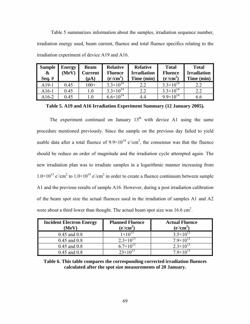
Table 5 summarizes information about the samples, irradiation sequence number,
irradiation energy used, beam current, fluence and total fluence specifics relating to the
irradiation experiment of device A19 and A16.
Sample &
Seq. #
Energy (MeV)
Beam Current
(µA)
Relative Fluence (e-/cm2)
Relative Irradiation Time (min)
Total Fluence (e-/cm2)
Total Irradiation Time (min)
A19-1 0.45 100+ 3.3×10¹⁴ 2.2 3.3×10¹⁴ 2.2 A16-1 0.45 1.0 3.3×10¹⁴ 2.2 3.3×10¹⁴ 2.2 A16-2 0.45 1.0 6.6×10¹⁴ 4.4 9.9×10¹⁴ 6.6
Table 5. A19 and A16 Irradiation Experiment Summary (12 January 2005).
The experiment continued on January 13th with device A1 using the same
procedure mentioned previously. Since the sample on the previous day failed to yield
usable data after a total fluence of 9.9×10¹⁴ e-/cm2, the consensus was that the fluence
should be reduce an order of magnitude and the irradiation cycle attempted again. The
new irradiation plan was to irradiate samples in a logarithmic manner increasing from
1.0×10¹³ e-/cm2 to 1.0×10¹⁵ e-/cm2 in order to create a fluence continuum between sample
A1 and the previous results of sample A16. However, during a post irradiation calibration
of the beam spot size the actual fluences used in the irradiation of samples A1 and A2
were about a third lower than thought. The actual beam spot size was 16.6 cm2.
Incident Electron Energy (MeV)
Planned Fluence (e-/cm2)
Actual Fluence (e-/cm2)
0.45 and 0.8 1×10¹³ 3.5×10¹²
0.45 and 0.8 2.3×10¹³ 7.9×10¹²
0.45 and 0.8 6.7×10¹³ 2.3×10¹³
0.45 and 0.8 23×1013 7.9×10¹³
Table 6. This table compares the corresponding corrected irradiation fluences calculated after the spot size measurements of 20 January.
69
Using the corrected fluences of Table 6, sample A1 was initially irradiated at an
actual fluence of 3.5×10¹² e-/cm2, A1-1, while the device was left in the off mode, the
VDG was turned off and the current integrator disconnected from the cold head. The cold
head ground was then shorted to the Keithley system ground and CV measurements were
taken. An initial short measurement cycle from –1V to 0V was used to attempt to flush
out any excess stored charge since the first few readings of the previous device initially
measured extremely high capacitance levels of 9.9×1030 F. This procedure worked and
the seven cycle measurements recorded usable capacitance data. The experiment
continued by disconnecting the measurement equipment, turning the VDG on, and
irradiating the sample to 7.9×10¹² e-/cm2, A1-2, or a fluence approximately two and a
quarter times the initial fluence, yielding a total fluence of 1.14×10¹³ e-/cm2
corresponding to a little more than three and a quarter times the initial fluence. A third
irradiation of the sample to 2.3×10¹³ e-/cm2, A1-3, or a fluence six and a half times the
initial fluence, yielding a total fluence of 3.44×10¹³ e-/cm2 which corresponds to ten times
the initial fluence. The fourth and final irradiation of 7.9×10¹³ e-/cm2, A1-4, or twenty-
two times the initial fluence ultimately made the total fluence of sample A1 roughly
equivalent to that received by A16. Thus establishing a fluence continuum from 1.0×10¹²
e-/cm2 to 1.0×10¹⁵ e-/cm2. Measurements were also taken immediately after warming the
cold head to room temperature and disconnecting the cold head from the beam tube.
Table 7 summarizes the pertinent information about the sample, irradiation
sequence number, irradiation energy used, beam current, fluence and total fluence
specifics relating to the irradiation experiment of A1.
70

Sample &
Seq. #
Energy (MeV)
Beam Current
(µA)
Relative Fluence (e-/cm2)
Relative Irradiation Time (min)
Total Fluence (e-/cm2)
Total Irradiation Time (min)
A1-1 0.45 0.15 3.5×10¹² 3 3.5×10¹² 3 A1-2 0.45 0.10 7.9×10¹² 7 1.14×10¹² 10 A1-3 0.45 0.13 2.3×10¹³ 10.2 3.44×10¹³ 20.2 A1-4 0.45 0.13 7.9×10¹³ 35.1 1.13×10¹⁴ 55.3
Table 7. A1 Irradiation Experiment Summary (13 January 2005).
The final irradiation iteration on January 14th also followed the previously
described procedure but involved electrons with energy of 0.8 MeV. A different energy
level was used in order to determine if higher energy electrons would create any
observable changes or alternate effects as compared to lower energy electrons.
A2 was used as the experimental sample during the final irradiations since it
possessed similar device parameters compared to A1. Again, the procedure followed was
the same as the previous day; however, sample A2 was initially subjected to 0.8 MeV
electrons and a fluence of 3.5×10¹² e-/cm2, A2-1. After a short irradiation, data
measurements were made resulting in usable numbers. The experiment continued by
disconnecting the measurement equipment, turning the VDG on, and irradiating the
sample to 7.9×10¹² e-/cm2, A2-2, or a fluence approximately two and a quarter times the
initial fluence, yielding a total fluence of 1.14×10¹² e-/cm2 corresponding to a little more
than three and a quarter times the initial fluence. After the second irradiation, data
measurements were made again resulting in usable data. A third irradiation of the sample
to 2.3×10¹³ e-/cm2, A2-3, or a fluence six and a half times the initial fluence, yielding a
total fluence of 1.0×10¹⁴ e-/cm2 also corresponding to ten times the initial fluence. After
the third irradiation however, temperature control was lost during data collection due to a
loss of pressure inside the liquid nitrogen tank. The tank started out full at the beginning
71
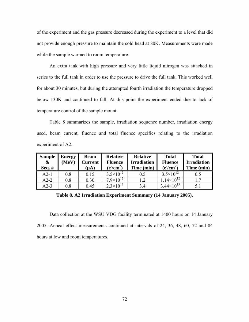
of the experiment and the gas pressure decreased during the experiment to a level that did
not provide enough pressure to maintain the cold head at 80K. Measurements were made
while the sample warmed to room temperature.
An extra tank with high pressure and very little liquid nitrogen was attached in
series to the full tank in order to use the pressure to drive the full tank. This worked well
for about 30 minutes, but during the attempted fourth irradiation the temperature dropped
below 130K and continued to fall. At this point the experiment ended due to lack of
temperature control of the sample mount.
Table 8 summarizes the sample, irradiation sequence number, irradiation energy
used, beam current, fluence and total fluence specifics relating to the irradiation
experiment of A2.
Sample &
Seq. #
Energy (MeV)
Beam Current
(µA)
Relative Fluence (e-/cm2)
Relative Irradiation Time (min)
Total Fluence (e-/cm2)
Total Irradiation Time (min)
A2-1 0.8 0.15 3.5×10¹² 0.5 3.5×10¹² 0.5 A2-2 0.8 0.30 7.9×10¹² 1.2 1.14×10¹² 1.7 A2-3 0.8 0.45 2.3×10¹³ 3.4 3.44×10¹³ 5.1
Table 8. A2 Irradiation Experiment Summary (14 January 2005).
Data collection at the WSU VDG facility terminated at 1400 hours on 14 January
2005. Anneal effect measurements continued at intervals of 24, 36, 48, 60, 72 and 84
hours at low and room temperatures.
72

V. Experimental Results
Irradiation Experiment: Sample A19
The first irradiation sequence, A19-1, was not successful in producing any usable
post-irradiation C-V data at low temperature. The fact that measuring usable data was not
likely was immediately recognized during irradiation since the beam current was 100 µA
when calculations indicated that it should have been around 1 µA. Prior to taking data the
device was identified as having failed and the subsequent attempt to measure capacitance
corroborated this belief. The capacitance measured while at low temperature sent the
Keithley 590 into compliance measurement indicating that the capacitance was extremely
large.
Data obtained immediately after irradiation at room temperature resulted in a
capacitance measurement, but not a recognizable characteristic C-V curve. Figure 40
below indicates an increase in capacitance in the low gate voltage region corresponding
to the inversion region in a characteristic C-V curve followed by a drop in capacitance in
the accumulation region. During and immediately after irradiation, device A19 failed to
operate as designed.
Subsequent room temperature annealing for 60 hours and measurements at 80K
and room temperature failed to exhibit any recovery in the device at all. This failure to
recover is attributed to the damage caused by the extremely high initial beam current.
73

A19-1 Irradiation with fluence of 3.3E14 e/cm2 @ RT
0
5E-12
1E-11
1.5E-11
2E-11
2.5E-11
-6 -5 -4 -3 -2 -1 0
Gate Voltage [V]
Cap
acita
nce
[F]
Pre-IrradiationPost-Irradiation 1E14 e/cm2
Figure 40. Pre- and Post-Irradiation capacitance-voltage measurements of A19 recorded at room temperature.
Irradiation Experiments: Sample A16
The second device, A16, produced results closer to expectation. Figure 41 shows
the change in capacitance as a result of irradiation by 0.45 MeV electrons and a fluence
of 3.3×10¹⁴ e-/cm2 in irradiation A16-1. The effects of this fluence are clearly seen as shift
of the flat-band and threshold voltages to the negative indicating an increase in interface
trapped charge. Also, a slight decrease in the capacitance is indicated in the depletion
region corresponding to the GaN, while there is no apparent increase or decrease in the
capacitance in the accumulation region relating to the AlGaN.
After the second irradiation, A16-2, at a total fluence of 9.9×10¹⁴ e-/cm2, the
capacitance measurements recorded at 80K were extremely high (9.9×1030 F) and
ultimately were unusable data. However in Figure 42, room temperature data recorded
immediately after irradiation, resulted in a characteristic C-V curve indicating a slight
74

decrease in capacitance between the pre-irradiation and post-irradiation curve, and a
recovery in device operation after a short room temperature anneal of approximately 5
minutes. The fact that the device failed to exhibit a characteristic C-V curve at low
temperature is not surprising since device A0408 was initially reported as having failed
after receiving a similar fluence [21] at a beam current that was an order of magnitude
less than that experienced by A16-2.
After 60 hours of room temperature annealing Figure 41 shows and overall
decrease in capacitance in all regions and a shift positive when compared with both pre-
and post-irradiation data. After a total of 84 hours of room temperature annealing, the
curve almost mirrors the initial pre-irradiation curve except for the slight negative
threshold voltage shift.
A16-1 Irradiation with fluence of 3.3E14 e/cm2 @ 80K with Anneal Comparison
02468
101214161820
-6 -5 -4 -3 -2 -1 0
Gate Voltage [V]
Cap
acita
nce
[pF]
Pre-IrradationPost-Irradiation 3.3E14 e/cm2After 60 hr RT annealAfter 84 hr RT anneal
Figure 41. A16 Pre- and Post-Irradiation capacitance-voltage measurements recorded at low temperature (~80K) plotted with 60- & 84-hour room temperature
anneal curves.
75

A16-2 Irradiation with fluence 6.6E14 e/cm2 @ RT
0
5
10
15
20
25
-6 -4 -2 0
Gate Voltage [V]
Cap
acita
nce
[pF]
Pre-Irradiation
Post-Irradiation 9.9E14 e/cm2
Figure 42. A16 Pre- and Post-Irradiation capacitance-voltage measurements at
room temperature.
Irradiation Experiments: Sample A1
The third sample, A1, produced capacitance measurements exactly as expected
during irradiation A1-1. Figure 43 below clearly shows an increase in the capacitance in
the inversion region of the curve as well as in the accumulation region of the curve after
experiencing a fluence of 3.5×10¹² e-/cm2. The increase in capacitance in the inversion
region yields an increase in the carrier concentration as presented in Figure 44. These
concentrations were calculated using equation (21). Additionally, the curve shifts more
negative and the threshold voltage decreases from a pre-irradiation –4.3V to a post-
irradiation VTH of –5.0V. This shift in threshold voltage is also an expected result.
76

A1-1 Irradiation with fluence of 3.5E12 e/cm2
0
5
10
15
20
25
-6 -5 -4 -3 -2 -1 0
Gate Voltage [V]
Cap
acita
nce
[pF]
Pre-Irradiation 80K1st Irradiation 3.5e12 e/cm2
Figure 43. Pre- and Post-Irradiation capacitance-voltage measurements of device A1 recorded at low temperature (~80K) after a fluence of 3.5×10¹² e/cm2 with 0.45 MeV
electrons.
Carrier Concentration Comparison A1-1 @ 80K
0.00E+00
2.00E+17
4.00E+17
6.00E+17
8.00E+17
1.00E+18
1.20E+18
1.40E+18
-6 -5.8 -5.6 -5.4 -5.2 -5 -4.8 -4.6
Gate Voltage [V]
Car
rier C
once
ntra
tion
[cm
-3]
Pre-IrradiationAfter 1st Irradiation 3.5e12 e/cm2
Figure 44. Pre- and Post-Irradiation carrier concentrations of device A1 recorded at low temperature (~80K) after a fluence of 3.5×10¹² e/cm2 with 0.45 MeV electrons.
77

The second data set, A1-2, measured after an additional fluence of 7.9×10¹² e-/cm2
and a total fluence of 1.14×10¹² e-/cm2 resulted in C-V curves for A1 that appeared to be
very non-characteristic when plotted with characteristic curves. However, on a smaller
scale the curves possess similar characteristics of the usual C-V curve, but there is a
larger inversion region and very little if any accumulation region. During measurement,
the capacitance did not converge around a specific value as all previous seven cycle
measurements had before. The tendency was a slight creep of increasing capacitance
during each subsequent cycle measurement. Figure 45 below graphically demonstrates
the change in capacitance during cycle measurement.
A1-2 Irradiation with fluence of 7.9E12 e/cm2
1.90E-12
2.00E-12
2.10E-12
2.20E-12
2.30E-12
2.40E-12
2.50E-12
2.60E-12
2.70E-12
2.80E-12
-6 -5 -4 -3 -2 -1 0
Gate Voltage [V]
Cap
acita
nce
[F] First Cycle
Second CycleThird Cyclefourth CycleFifth CycleSixth CycleSeventh Cycle
Figure 45. A1 Post-Irradiation capacitance-voltage measurements at low temperature (~80K) after a fluence of 7.9×10¹² e/cm2 with 0.45 MeV electrons.
78

A1-3 Irradiation with fluence of 2.3E13 e/cm2
3.00E-12
3.50E-12
4.00E-12
4.50E-12
5.00E-12
5.50E-12
-6 -5 -4 -3 -2 -1 0
Gate Voltage [V]
Cap
acita
nce
[F] Cycle 1
Cycle 2Cycle 3Cycle 4Cycle 5Cycle 6Cycle 7
Figure 46. A1 Post-Irradiation capacitance-voltage measurements at low
temperature (~80K) after a fluence of 2.3×10¹³ e/cm2 with 0.45 MeV electrons.
The third data set, A1-3, measured after an additional fluence of 2.3×10¹³ e-/cm2
culminating in a total fluence of 3.44×10¹³ e-/cm2 appeared very similar to data obtained
after the second irradiation. However, the capacitance measured was about twice that
measured previously. Additionally, the increase around 0V in the second set is much less
pronounced than in the third set producing a much more uniform curve as observed in
Figure 46.
The fourth irradiation, A1-4, at a fluence of 7.9×10¹³ e-/cm2 resulted in a
capacitance measurement that exceeded the Keithley 590 CV capabilities resulting in
unusable numbers around 9.9×1030 F.
Figure 47 below compares all three irradiation iterations (A1-1, A1-2, and A1-3)
that resulted in usable data and except for A1-2 there is a definite increase in capacitance
in the inversion region of the curve. A1-2 and A1-3 appear to indicate that the entire
79

device is operating as though it were in inversion from the gate through the GaN as there
is no characteristic depletion or accumulation region.
Irradiation Comparison A1-1, A1-2, & A1-3 @ 80K
0
5
10
15
20
25
-6 -5 -4 -3 -2 -1 0
Gate Voltage [V]
Cap
acita
nce
[pF]
Pre-IrradiationFirst Irradiation 3.5E12 e/cm2Second Irradiation 7.9E12 e/cm2Third Irradiation 2.3E13 e/cm2
Figure 47. Comparison of Sample A1 Pre-Irradiation C-V data with subsequent irradiation C-V data at fluence levels of 3.5×10¹² e/cm2, 7.9×10¹² e/cm2 and 2.3×10¹³
e/cm2 with 0.45 MeV electrons.
Using the data in Figure 47, the carrier concentrations for all irradiation iterations
of sample A1 were calculated using equation (21). Figure 48 shows an increase in carrier
concentration as a result of irradiation as the general trend. The second irradiation, A1-2,
appears out of order and somewhat anomalous; however, the third irradiation, A1-3,
indicates an increase in capacitance over all previous curves with respect to the inversion
region.
80

Carrier Concentration Comparision A1-1, A1-2, & A1-3 @ 80K
0.00E+001.00E+172.00E+173.00E+174.00E+175.00E+176.00E+177.00E+178.00E+179.00E+171.00E+18
-6 -5.5 -5 -4.5
Gate Voltage [V]
Car
rier C
once
ntra
tion
[cm
-3]
Pre-IrradiationFirst Irradiation 3.5E12 e/cm2Second Irradiation 7.9E12 e/cm2Third Irradiation 2.3E13 e/cm2
Figure 48. A1 Pre- and Post-Irradiation carrier concentrations at low temperature (~80K) after irradiation at fluence levels of 3.5×10¹² e/cm2, 7.9×10¹² e/cm2 and
2.3×10¹³ e/cm2 with 0.45 MeV electrons.
The room temperature measurements recorded immediately after irradiation, again
resulted in a characteristic C-V curve as they did for A16-2. Figure 49 shows that there is
a clear increase in capacitance between the pre-irradiation and post-irradiation curve in
the inversion region and a decrease in capacitance in the accumulation region. The
measurement after a thirty-six-hour room temperature anneal also clearly shows an
increase in capacitance over pre-irradiation values and post-irradiation levels. Although
the post-irradiation capacitance in the accumulation region is less than that measured pre-
irradiation, the measurements after a thirty-six hour anneal have increased with respect to
the measurements recorded immediately after irradiation at room temperature. Charge
appears to be increasing over time in the accumulation region as the device remains at
room temperature.
81

A1-4 Anneal Comparison @ RT
02468
101214161820
-6 -5 -4 -3 -2 -1 0
Gate Voltage [V]
Cap
acita
nce
[pF]
Pre-IrradiationPost-IrradiationAfter 36 hour RT annealAfter 72 hour RT anneal
Figure 49. A1 Pre- and Post-Irradiation capacitance-voltage measurements at room temperature after a total fluence of 1.13×10¹⁴ e/cm2 and compared with the 36 and
72-hour room temperature anneal curve.
After 48 hours of room temperature annealing, Figure 50 shows that the
capacitance level in the inversion region has returned to pre-irradiation levels, while the
curve has dropped below pre-irradiation levels in the accumulation region. There is also a
slight decrease in slope in depletion indicating trapped interface charge. There are
definite permanent changes due to irradiation that anneal somewhat but not completely.
82

A1 Anneal Comparison @ 80K
0
5
10
15
20
25
-6 -5 -4 -3 -2 -1 0
Gate Voltage [V]
Cap
acita
nce
[pF]
Pre-IrradiationFirst Irradiation 3.5E12 e/cm2After 48 hr RT annealAfter 72 hr RT anneal
Figure 50. A1 Pre- and Post-Irradiation capacitance-voltage measurements at low temperature after a total fluence of 1.13×10¹⁴ e/cm2 compared with the 48 and 72-
hour room temperature anneal curves.
In Figure 51 the carrier concentration is plotted using information from the
inversion region in the curves in Figure 50 and yields a 2-3 times increase in carrier
concentration when measured at room temperature.
A1 Carrier Concentration Comparision @ RT
01E+172E+173E+174E+175E+176E+177E+178E+179E+171E+18
-6 -5.8 -5.6 -5.4 -5.2 -5 -4.8 -4.6
Gate Voltage [V]
Car
rier C
once
ntra
tion
[cm
-3]
Pre-Irradiation
First Irradiation 3.5E12 e/cm2
Second Irradiation 7.9E12e/cm2Third Irradiation 2.3E13 e/cm2
After 48 hour RT anneal
Figure 51. A1 Pre- and Post-Irradiation carrier concentrations at room temperature with carrier concentration of 48-hour room temperature anneal data.
83

Irradiation Experiments: Sample A2
Sample A2 produced capacitance in total contrast to any recorded previously either
at room or low temperature, and whether or not the device had been irradiated. Iteration
A2-1 irradiated sample A2 with 0.8 MeV electrons and a fluence of 3.5×10¹² e-/cm2. The
procedure followed was the same as in the previous iterations and measurements were
recorded in the same manner at low temperature. However, during the initial sweep of
-1V to 0V that had previously been used to clear extraneous charge from initial
measurements of other devices, the Keithley 590 recorded capacitance values within the
measurement capabilities of the analyzer immediately. The interesting part about the
capacitance measurements of A2-1 was that instead of positive capacitance in the pF
range, this time the capacitance measured was in the negative pF range. While continuing
to take measurements, a rapid check of the lead connections ensured that the device was
properly connected and not grounded to any extraneous connection around the beam
tube. Figure 52 clearly shows a negative capacitance measurement after A2-1 and Figure
53 shows the first measurement compared with the pre-irradiation data highlighting the
negative capacitance measurements. These negative values for capacitance indicate that
the analyzer is measuring the capacitance of something with an opposite charge to that
measured in the previous heterostructures.
84

A2-1 Irradiation with fluence of 3.5E12 e/cm2 @ 80K
-9.00E-01
-8.00E-01
-7.00E-01
-6.00E-01
-5.00E-01
-4.00E-01
-3.00E-01
-2.00E-01
-1.00E-01
0.00E+00
-6 -5 -4 -3 -2 -1 0
Gate Voltage [V]
Cap
acita
nce
[pF]
Post-Irradiation 3.5E12 e/cm2
Figure 52. A2 Post-Irradiation capacitance-voltage measurements at low temperature (~80K) after a fluence of 3.5×10¹² e/cm2 with 0.8 MeV electrons.
A2-1 Irradiation with fluence of 3.5E12 e/cm2 @ 80K
-5
0
5
10
15
20
-6 -5 -4 -3 -2 -1 0
Gate Voltage [V]
Cap
acita
nce
[pF]
Pre-Irradiation 80KPost-Irradiation 3.5E12 e/cm2
Figure 53. A2 Pre- and Post-Irradiation capacitance-voltage measurements at low
temperature (~80K) after a fluence of 3.5×10¹² e/cm2 with 0.8 MeV electrons.
85

The second seven-cycle measurement, A2-2, produced the same negative
capacitance effect although the values were slightly more positive than the first
measurements.
A2-2 Irradiation with fluence of 7.9E12 e/cm2 @ 80K
-5
0
5
10
15
20
-6 -5 -4 -3 -2 -1 0
Gate Voltage [V]
Cap
acita
nce
[pF]
Pre-IrradiationSecond Irradiation 7.9E12 e/cm2
Figure 54. A2 Pre- and Post-Irradiation capacitance-voltage measurements at low temperature (~80K) after a fluence of 7.9×10¹² e/cm2 with 0.8 MeV electrons.
The third measurement set, A2-3, depicted in Figure 55 was interrupted by a loss
of temperature control; however, during the slow rise in temperature from 80K to 192K
capacitance measurements continued. The measurements showed a general trend of
increasing negative capacitance in each subsequent cycle as the temperature increased.
Figure 56 highlights the change between pre-irradiation capacitance levels and the
capacitance after the third irradiation, A2-3, at 2.3×10¹³ e-/cm2. Although, the loss in
temperature control makes the interpretation and comparison of the third set of data with
previous sets difficult and inconclusive in isolation (Figure 57), the important fact is that
the capacitance of the third set was negative just as the previous two data sets were
86

(Figure 58). The negative capacitance indicates that charges of opposite polarity are
measured due to electron irradiation by electrons with incident energy of 0.8 MeVs.
A2-3 Irradiation with fluence of 2.3E13 e/cm2 @ 80K
-2.50E-11
-2.00E-11
-1.50E-11
-1.00E-11
-5.00E-12
0.00E+00-6 -5 -4 -3 -2 -1 0
Gate Voltage [V]
Cap
acita
nce
[F] Cycle 1
Cycle 2Cycle 3Cycle 4Cycle 5Cycle 6Cycle 7
Figure 55. A2 Post-Irradiation capacitance-voltage at low temperature (~80K) after
a fluence of 2.3×10¹³ e/cm2 with 0.8 MeV electrons.
A2-3 Irradiation with fluence of 2.3E13 e/cm2 @ 80K
-20
-15
-10
-5
0
5
10
15
20
25
-6 -5 -4 -3 -2 -1 0
Gate Voltage [V]
Cap
acita
nce
[pF]
Pre-Irradiation 80KPost-Irradiation 2.3E13 e/cm2
Figure 56. A2 Pre- and Post-Irradiation capacitance-voltage measurements at low
temperature (~80K) after a fluence of 2.3×10¹³ e/cm2 with 0.8 MeV electrons.
87

Irradiation Comparision A2-1, A2-2 and A2-3 @ 80K
-16-14-12-10-8-6-4-202
-6 -5 -4 -3 -2 -1 0 1
Gate Voltage [V]
Cap
acita
nce
[pF]
1st Irrad 3.5E12 e/cm22nd irrad 7.9E12 e/cm23rd Irrad 2.3E13 e/cm2
Figure 57. Comparison of irradiation C-V data at fluence levels of 3.5×10¹² e/cm2,
7.9×10¹² e/cm2 and 2.3×10¹³ e/cm2 with 0.8 MeV electrons.
A2 Irradiation Comparison @ 80K
-20-15-10-505
10152025
-6 -5 -4 -3 -2 -1 0
Gate Voltage [V]
Cap
acita
nce
[pF]
Pre-Irradiation 80K1st Irrad 3.5E12 e/cm22nd Irrad 7.9E12 e/cm23rd Irrad 2.3E13 e/cm2
Figure 58. Comparison of Pre-Irradiation C-V data with subsequent irradiation C-V data at fluence levels of 3.5×10¹² e/cm2, 7.9×10¹² e/cm2 and 2.3×10¹³ e/cm2 with
0.8 MeV electrons showing negative increase in capacitance.
88

The room temperature measurements for device A2 recorded immediately after
irradiation, A2-3, again resulted in a characteristic C-V curve (Figure 59) as did A16-2
and A1-4; however, the capacitance measurements continued to increase negatively as the
anneal process progresses. There is a slight decrease in capacitance between the pre-
irradiation and 24 hour anneal curve in the inversion region and a slight increase in
capacitance in the accumulation region with an apparent no change in depletion.
A2-3 Anneal Comparison @ RT
0
5
10
15
20
25
-6 -5 -4 -3 -2 -1 0
Gate Voltage [V]
Cap
acita
nce
[pF]
Pre-IrradiationPost-IrradiationAfter 24 hour RT annealAfter 60 hour RT anneal
Figure 59. A2 Pre- and Post-Irradiation capacitance-voltage measurements at room temperature after a total fluence of 1.14×10¹⁴ e/cm2 and compared with the 24 & 60
hour room temperature anneal curves. The 36 and 60 hour anneal measurements at 80K revealed a characteristic C-V
curve in Figure 60 with positive capacitance values indicating that the major damage due
to 0.8 MeV electrons annealed after exposure to room temperature. Both anneal curves
show a shift in the negative direction with a more negative threshold voltage of –5V
compared to a pre-irradiation VTH of –4.3V. There is also a recovery toward the pre-
89

irradiation curve in all regions in both anneal curves except for the threshold voltage
shift. In this manner, the damage due to a fluence of 1.14×10¹⁴ e-/cm2 is permanent.
A2 Anneal Comparison
0
2
46
8
10
12
1416
18
20
-6 -4 -2 0
Gate Voltage [V]
Cap
acita
nce
[pF]
Pre-Irradiation 80KAfter 36 hour RT annealAfter 60 hour RT anneal
Figure 60. A2 Pre-Irradiation capacitance-voltage measurement at low temperature after a total fluence of 1.14×10¹⁴ e/cm2 compared with the 36 and 60 hour room
temperature anneal curves.
Previously Irradiated Samples: A0408 and A0409
During the eight-week maintenance period of the WSU VDG irradiation of
samples was not possible. In light of this, the two surviving samples (A0408 and A0409)
irradiated on 28 January 2004 by [21] have been analyzed with respect to the effects of
low energy electron irradiation as well as room temperature annealing effects after 9
months in order to attempt to explain the observations in previous research [21].
The 9 new samples were pre-characterized and measured by the Keithley 590 C-V
analyzer in order to produce capacitance versus gate voltage curves for analysis. Each
90
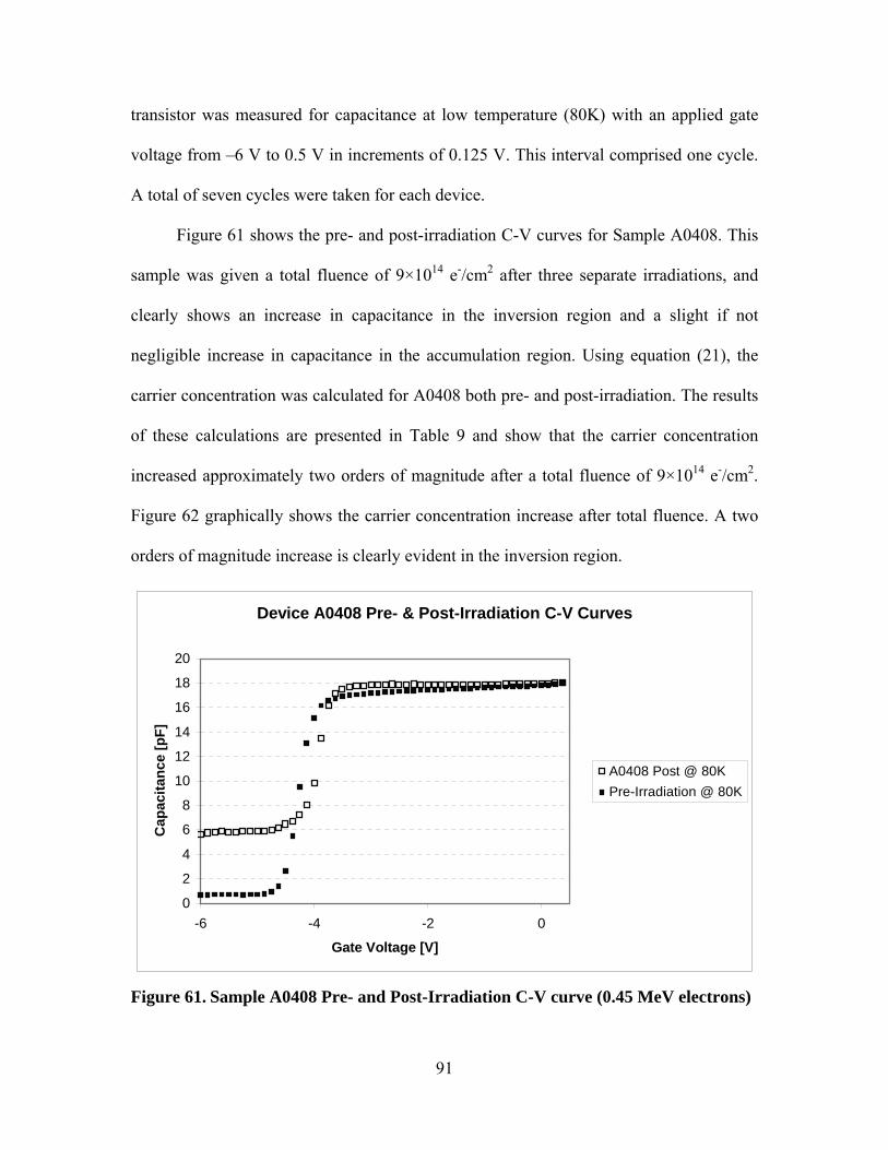
transistor was measured for capacitance at low temperature (80K) with an applied gate
voltage from –6 V to 0.5 V in increments of 0.125 V. This interval comprised one cycle.
A total of seven cycles were taken for each device.
Figure 61 shows the pre- and post-irradiation C-V curves for Sample A0408. This
sample was given a total fluence of 9×10¹⁴ e-/cm2 after three separate irradiations, and
clearly shows an increase in capacitance in the inversion region and a slight if not
negligible increase in capacitance in the accumulation region. Using equation (21), the
carrier concentration was calculated for A0408 both pre- and post-irradiation. The results
of these calculations are presented in Table 9 and show that the carrier concentration
increased approximately two orders of magnitude after a total fluence of 9×10¹⁴ e-/cm2.
Figure 62 graphically shows the carrier concentration increase after total fluence. A two
orders of magnitude increase is clearly evident in the inversion region.
Device A0408 Pre- & Post-Irradiation C-V Curves
0
2
4
6
8
10
12
14
16
18
20
-6 -4 -2 0
Gate Voltage [V]
Cap
acita
nce
[pF]
A0408 Post @ 80KPre-Irradiation @ 80K
Figure 61. Sample A0408 Pre- and Post-Irradiation C-V curve (0.45 MeV electrons)
91

A0408 Carrier Concentration Pre- & Post-Irradiation @ 80 K
1E+15
1E+17
2E+17
3E+17
4E+17
5E+17
6E+17
-6 -5.8 -5.6 -5.4 -5.2 -5 -4.8 -4.6 -4.4
Gate Voltage [V]
Car
rier C
once
ntra
tion
[cm
-3]
Pre-IrradiationPost-Irradiation
Figure 62. Sample A0408 Pre- and Post-Irradiation Carrier Concentration
Figure 62 shows the pre- and post-irradiation C-V curves for Sample A0409. This
sample was given a total fluence of 3.67×10¹⁵ e-/cm2 after a total of four irradiations, and
clearly shows a large increase in capacitance in the inversion region and a smaller
increase in capacitance in the accumulation region. Using equation (21), the carrier
concentration was calculated for A0409 both pre- and post-irradiation. The results of
these calculations are presented in Table 9 and show that the carrier concentration
increased three orders of magnitude after a total fluence of 3.67×10¹⁵ e-/cm2. Figure 64
graphically shows the carrier concentration increase after total fluence. A three orders of
magnitude increase is clearly evident in the inversion region. The slope of the post-
irradiation curve in the depletion region is also flatter than the pre-irradiation curve
indicating trapped charge at the interface.
92

Device A0409 Pre- & Post-Irradiation C-V Curves
0
5
10
15
20
25
-6 -4 -2 0
Gate Voltage [V]
Cap
acita
nce
[pF]
A0409 Post @ 80KPre-Irradiation @ 80K
Figure 63. Sample A0409 Pre- and Post-Irradiation C-V curve (0.45 MeV electrons)
A0409 Pre- & Post-Irradiation Carrier Concentration
1E+15
5E+17
1E+18
2E+18
2E+18
3E+18
-6 -5.5 -5 -4.5
Gate Voltage [V]
Car
rier C
once
ntra
tion
[cm
-3]
Pre-IrradiationPost-Irradiation
Figure 64. Sample A0409 Pre- and Post-Irradiation Carrier Concentration
93

A0408 9 and 12 Month Anneal Comparison
0
5
10
15
20
-6 -5 -4 -3 -2 -1 0
Gate Voltage [V]
Cap
acita
nce
[pF]
9 Month Anneal 80K12 Month Anneal 80KPre-Irradiation80K
Figure 65: Comparison of CV curves for A0408 after a nine and twelve-month room
temperature anneal measured at 80K.
A0409 9 and 12 Month Anneal Comparison
0
5
10
15
20
25
-6 -5 -4 -3 -2 -1 0
Gate Voltage [V]
Cap
acita
nce
[pF]
9 Month Anneal 80K12 Month Anneal 80KPre-Irradiation 80K
Figure 66: Comparison of CV curves for A0409 after a nine and twelve-month room
temperature anneal measured at 80K.
As initially stated, device A0408 and A0409 annealed at room temperature
conditions from the 28th of January 2003 until the 22nd of October 2004 when the first
94

capacitance-voltage measurements were conducted. The elapsed time was just under nine
months. The expectation is that any of these devices left to anneal at room temperature
would respond in a similar manner taking into account the incident electron energy and
the total fluence experienced.
On the 16th of December 2004, twelve months after irradiation a second set of
capacitance-voltage measurements were recorded in order to observe the effects of a 12-
month room temperature anneal. Again, as with the previous measurements of A0408 and
A0409, the results of both devices were different. As Figure 65 shows the capacitance
increases in all regions of the curve for A0408 with a negative threshold voltage shift
back toward the pre-irradiation curve. This would apparently show that hole traps in the
AlGaN layer are increasing rather than annealing away. A0409 in Figure 66 shows a
decrease in all areas of the curve with respect to the nine-month anneal curve and the
accumulation region of the pre-irradiation curve. This demonstrates that the hole traps are
annealing due to tunneling to a point that below that of the pre-irradiation capacitance
level. A positive threshold voltage shift is noted in A0409 toward pre-irradiation levels
that are consistent with the observations in A0408 in that both VTH tend back toward the
pre-irradiation VTH. The fact that the accumulation region over annealed past the pre-
irradiation capacitance for A0409 may be attributed to the fact that the pre-irradiation
curve is an average of nine non-irradiated devices and may not reflect the exact nature of
the pre-irradiation capacitance of A0409.
The results of A0408 and A0409 are consistent with the annealing of A1 and A2 in
that A1 and A2 also over annealed and then showed a trend back to pre-irradiation levels.
95

Analysis and Discussion
In previous research [21], an unexplained result of irradiation was a large increase
in drain current. At the time, the C-V measurements required to explain these results were
unavailable. However, this research has conducted the required measurements needed to
explain the phenomenon.
Using Equation (20) as the mathematical model that describes the drain current, IDS
is directly related to four variables: the charge of an electron, the width of the gate, the
electron mean velocity in the channel, and the channel sheet charge density. Since both
the charge of an electron and the gate width are constants, this indicates that any change
in drain current must be caused by either a change in the channel sheet charge density
(the 2DEG carrier concentration) or a change in the electron mean velocity in the
channel. Capacitance measurements from experiment were used to calculate the carrier
concentration before irradiation and after irradiation by electrons. The increase in
capacitance resulted in an increase in carrier concentration indicating that the drain
current increase was caused by a direct increase in carrier concentration in the 2DEG.
Device ID
Voltage [V]
Capacitance [F]
Pre-
Irradiation
Carrier Concentration
[cm-3] Pre-
Irradiation
Capacitance [F]
Post-
Irradiation
Carrier Concentration
[cm-3] Post-
Irradiation
Order Magnitude
Of Change [cm-3]
A0408 -5 7.375×10⁻¹³ 8.52×10¹⁵ 5.922×10⁻¹² 5.49×10¹⁷ 2 A0409 -5 7.375×10⁻¹³ 8.52×10¹⁵ 1.089×10⁻¹¹ 1.86×10¹⁸ 3 A16 -5 2.04×10⁻¹² 6.53×10¹⁶ 1.66×10⁻¹² 4.32×10¹⁶ 0 A1 -5 2.75×10⁻¹² 1.19×10¹⁷ 4.11×10⁻¹² 2.66×10¹⁷ 0
Table 9: Comparison of device Pre- And Post-Irradiation Carrier Concentration.
96

In three of the four devices observed during this research effort, the major effect
was an increase in the capacitance in the inversion region after irradiation by 0.45 MeV
electrons. Table 9 shows the effects of this level of irradiation in the carrier concentration
of the 2DEG as calculated by equation (22).
The carrier concentration increase is caused by either an increase in positive charge
in the AlGaN layer and/or an increase in donor electrons from a nitrogen vacancy in the
gallium nitride.
The first explanation for the drain current increase is based on trapped charge in
the AlGaN layer. The AlGaN layer is extremely thin at 25 nm and as such any charge
trapped in the AlGaN layer would have an enormous effect on the electric field acting
upon charge carriers in the GaN layer. Essentially, any trapped charge would appear to
increase the gate voltage with respect to the charge carriers in the GaN. The result of an
increase in gate charge would be an increase in negative charge drawn up from the GaN
toward the interface to match the positive charge trapped in the AlGaN. This increase in
equal but opposite charge would appear as more charge on a parallel plate capacitor
resulting in increased capacitance in the accumulation region of the C-V curves. This is
in fact what is observed in samples A0408, A0409 and A1.
Electron radiation interacting with atoms in the AlGaN layer ionizes a large
amount of electrons. The massive amounts of ionization involved with this are supported
by the fact that collisional stopping power, which causes ionization and excitation,
accounts for the overwhelming majority of energy deposited in AlGaN [21]. The large
amounts of ionization involved are produced by relatively low fluences (1013 e-/cm2 to
1014 e-/cm2). These ionized electrons are temporarily trapped in energy states near the
97

conduction band of AlGaN. However, due to the application of a high electric field
through the gate voltage or the intrinsic electric field associated with the highly polarized
AlGaN heterostructure, these trapped electrons are immediately made mobile and swept
out of the AlGaN. In the first case, a positive applied gate voltage and the intrinsic
electric field draw the electrons to the gate whereas a negative gate voltage pushes the
electrons toward the GaN. The latter case results in negative charge collection at the
AlGaN/GaN heterointerface, which would then be added into the 2DEG.
In any event, this process results in the removal of numerous electrons from the
AlGaN layer, leaving behind a net stationary positive charge. This new stationary
positive charge would add to the overall net positive charge in the AlGaN layer (created
by polarization fields) resulting in an increase in the electric field seen by the potential
2DEG carriers in the GaN layer. The increased electric field (directed into the GaN layer)
would draw an increased number of mobile electrons out of the GaN layer and deposit
them into the 2DEG, yielding higher 2DEG carrier concentrations. As previously
indicated, this proposed process essentially involves the creation of a virtual gate voltage
similar to the threshold voltage shifting effect that occurs in electron irradiated
MOSFETs and which is observed Figure 50 and Figure 60.
The second explanation for an increase in the carrier concentration in the 2DEG is
through the formation of nitrogen vacancies that donate electrons to the GaN that are
deposited into the 2DEG. The nitrogen vacancy has been proposed by numerous sources
[18] [19] [27] as the impurity responsible for the n-type self-doping of gallium nitride and
major contributor to the 2DEG.
98

This experiment measured the capacitance of transistor devices irradiated using
0.45 MeV low energy electrons. The post-irradiation capacitance increased with respect
to the pre-irradiation capacitance levels. Through calculations these capacitance levels
were used to show that the carrier concentration in the 2DEG increased in the same
manner that doping concentration caused a vertical shift in the C-V curves of n-type
MOSFETs in Figure 26.
In a previous study, Look et al. [27] irradiated gallium nitride with 0.42 MeV
electrons and found that at that level of radiation only the nitrogen vacancy was a shallow
donor. Since 0.42 MeV and 0.45 MeV electrons are relatively close in energy, it is
proposed that the increase in carrier concentration observed in these devices is due to the
nitrogen vacancy contributing electrons in the gallium nitride and that these electrons are
subsequently drawn into the 2DEG by the inherent electric field in the AlGaN.
Look et al. [27] further state that the minimum energy required to produce nitrogen
displacement is 0.32 MeV and the minimum energy required to produce a gallium
displacement is 0.53 MeV. The when this displacement occurs a nitrogen atom can
donate and electron and a gallium atom accepts an electron. Furthermore, the production
of the nitrogen donors exceeds the formation of gallium acceptors up to energy of
approximately 0.87 MeV.
The increase due to the nitrogen vacancy in GaN should be easily observed by
irradiating the samples with various energy electrons from 0.4 MeV to 0.8 MeV. As the
energy increases the effects of donor electrons from the nitrogen should decrease as the
incoming electrons begin to interact with the gallium. Thus, the capacitance should
decrease when the C-V curves at higher electron energies are plotted and compared to the
99

plots of C-V curves of incident electrons with lower energies. During the irradiation of
sample A2, the incident electron energy was changed to 0.8 MeV in order to observe this
effect.
A slight decrease in capacitance in the inversion region between the 0.45 MeV
sample, A1, and the 0.8 MeV sample, A2, was initially expected; however, the complete
change in sign of the capacitance readings of A2 was unexpected. The following
explanation is proposed. The fact that the capacitance measurements for A2 were
negative indicates that the capacitance measured is due to the creation of acceptors in the
GaN layer whereas a measurement of positive capacitance indicates that the capacitance
measured is due to the creation of donors in the GaN. The GaN is intrinsically n-type
indicating a natural surplus of electrons. This explains why the initial capacitance
measurements are not equal in magnitude to the positive capacitance measurements and
why as the measurement cycles repeat the capacitance becomes less negative. The
intrinsic electrons are slowly filling the acceptors (holes) as the inherent electric field
between the AlGaN and GaN directs the electrons toward the GaN.
The effect of incident electrons (0.45 MeV) is ionization and the creation of
electron/hole pairs in the AlGaN. Due to the intrinsic electric field in the AlGaN, the
ionized electrons exit the heterostructure rapidly leaving behind a stationary and trapped
positive charge in the AlGaN along the interface between the AlGaN and GaN (Figure
67). This trapped positive charge along the interface causes more electrons from the bulk
GaN to populate the 2DEG requiring a more negative applied bias to turn the device off
and collapse the quantum well. The observed result of this trapped charge in the CV
curves is a negative curve shift along the gate voltage axis and a negative increase in the
100

threshold voltage (Figure 68). Also, Figures 37 and 39 clearly show this threshold
voltage shift following irradiation; however, Figure 57 and 59 show that after a 9 month
room temperature anneal, the curve has recovered to the pre-irradiation location. The
defect centers have been filled due to recombination through tunneling during the
annealing process.
Figure 67. Band diagram of AlGaN/GaN MODFET after irradiation by 0.45 MeV electrons showing increase in carrier concentration due to formation of VN in the
GaN that donate electrons to the 2DEG.
Figure 68. Negative threshold voltage shift in CV curve as a result of 0.45 MeV electron irradiation creating positive interface trapped charge.
101

102
The effect of incident electrons (0.8 MeV) is the formation of gallium vacancies in
the GaN. These gallium vacancies act as acceptors and draw electrons from the 2DEG
thus reducing the number of carriers and depopulating the quantum well. The gallium
vacancy (acceptor) has the effect of lowering the EBF B and depopulating the 2DEG.
Figure 69. Band diagram of AlGaN/GaN MODFET after irradiation by 0.8 MeV electrons showing decrease in carrier concentration due to formation of VBGa B in the
GaN that accept electrons from the heterostructure and 2DEG.
The capacitance in the Keithley 590 is calculated by the simple relationship,
fVIC /= (23)
where I is the measured current, f is the measurement frequency and V is the source
voltage. The frequency is a constant set by the operator depending on the output desired
and can be either 100 kHz or 1 MHz on the Keithley 590.
The negative capacitance measurement obtained during the data recording of
sample A2 is due to the way in which the Keithley 590 measures the capacitance through
equation (23). The only term in equation (23) that has the potential to change sign is V
due to a measured potential difference between the conduction band and the Fermi level
that is greater (Figure 69) compared to the measured potential from sample A1 (Figure
67). The Keithley 590 measures a current based on electrons inherently, and outputs a
positive capacitance. However, the 0.45 MeV incident electrons create nitrogen vacancies
(donors) in the AlGaN and GaN liberating electrons that populate the 2DEG and others
that exit the AlGaN under the influence of the intrinsic electric field, E. This is the normal
or positive measured capacitance and results in a positive capacitance measurement
through the Keithley 590. The 0.8 MeV incident electrons create gallium vacancies
(acceptors) in the GaN liberating holes that depopulate the 2DEG and create a more
positive charge in the normally n-doped GaN layer. Since the GaN is still under the
influence of the intrinsic electric field, E, the conduction band still bends somewhat at the
heterojunction forming a quantum well (Figure 69), but the quantum well has been
depopulated of electrons. This depopulation of the 2DEG and increase in positive charge
in the GaN accounts for the negative capacitance measurement by the Keithley 590.
Additionally, just as the room temperature anneal of A1 resulted in an increase in
measured capacitance as the annealing process progressed, the room temperature anneal
of A2 resulted in a decrease in measured capacitance as the annealing progressed. This
could indicate that the process liberating electrons and holes from the donors and
acceptors, respectively, continues after irradiation ceases with the result that there is a net
increase in stored charge in the donor case or a net decrease in stored charge in the
acceptor case.
103

VI. Conclusions and Recommendations
Conclusions
Irradiation of AlGaN /GaN HEMTs by low energy electrons creates temperature-
dependent damage that affects transistor operation. These effects have been observed in
the transistor through capacitance-voltage measurements. The transistors show an
increase in capacitance in the accumulation region and the inversion region as well as a
negative shift and moderate flattening of the slope in the depletion region. The increase in
capacitance in the inversion region indicates an increase in charge as a result of an
increase in carrier concentration in the 2DEG, while the increase in the accumulation
region indicates an increase in trapped positive charge in the AlGaN. The slope flattening
in depletion indicates the presence of trapped interface charge between the AlGaN and
GaN, which appears to be a permanent defect for the lower incident energy electron
irradiation. The devices consistently fail to operate as designed at total fluences of
1.0×10¹⁵ e-/cm2 and do not recover completely to pre-irradiation operating parameters
even after room temperature annealing.
The increase in carrier concentration in the 2DEG is due to low energy electron
irradiation of 0.45 MeVs most likely resulting in displaced nitrogen atoms creating
nitrogen vacancies. The nitrogen vacancies donate an electron to the GaN, which (due to
the inherent electric fields in the highly polarized AlGaN layer) is drawn into the 2DEG.
A second mechanism increasing the carrier concentration in the 2DEG is the deposition
of large amounts of energy into the AlGaN resulting in a huge amount of ionization. This
ionization results in the creation of electron-hole pairs in the AlGaN. Due to the intrinsic
104

electric field in the AlGaN, the electrons are swept out of the AlGaN and into the 2DEG
leaving behind a large amount of trapped positive charge. This trapped positive charge
increases the effect on the 2DEG by drawing more carriers from the bulk GaN increasing
the concentration of the carriers. Essentially, both processes play an integral role in
increasing the carrier concentration. The measurements obtained in this research do not
provide the requisite information to definitively state which process dominates and under
what conditions one dominates the other.
By conducting experiments at various energy levels ranging from energy that
creates nitrogen vacancies to energy that favors gallium vacancies, the effects on carrier
concentration were observed. The results indicate that the 2DEG increases at low electron
energies due to nitrogen vacancies acting as donors, and decreases at higher electron
energies due to gallium vacancies acting as acceptors.
Recommendations for Further Work
Due to the maintenance required by the VDG and the subsequent time constraints
to complete data collection, not all of the 9 samples prepared for irradiation were
irradiated. This leads to the requirement for additional research to validate the findings of
this research with more corroborative data. Ideally, two additional samples irradiated at
0.45 MeV that duplicated the results of A1 would reinforce the conclusion that carrier
concentration is indeed increasing due to irradiation. Likewise, at least two more
irradiations at 0.8 MeV are required to duplicate the negative capacitance measurements
and offer validation of the premise that gallium displacements are creating acceptors at
0.8 MeV while nitrogen vacancies are providing donors at a lower energy of 0.45 MeV.
105

Then, the proposed cause of the carrier concentration increase in the 2DEG can be
attributed to the nitrogen vacancy as a result of incident electron energy. Further research
should attempt to irradiate at a minimum with incident electrons at energies of 0.3, 0.5
and 0.7 MeV to observe changes in capacitance and determine where positive and
negative capacitance thresholds occur as well as where there is no change.
A study using DLTS to determine if low incident electron energy causes nitrogen
displacements and higher incident electron energy causes gallium displacements would
add further credence to the results presented and theory proposed in the preceding pages.
Another possible avenue of investigation would be positron annihilation
spectroscopy performed on samples irradiated with incident electron energy of 0.8 MeVs
or greater in order to determine if gallium vacancies are actually formed in the GaN.
Additionally, a combined study involving both I-V and C-V low temperature
measurements repeating both previous work and this research would produce concurrent
results that when compared would provide a more complete picture than that of the two
separate studies.
Finally, a computer simulation or model that replicates the device functioning
would be beneficial in analyzing and predicting the various radiation effects on the
HEMT devices. Specifically, the model should include the ability to input heterostructure
parameters such as those listed on Figure 30. Additionally, by inputting incident electron
energy, fluence and beam current, the output would yield capacitance information
relative to all three regions of interest (accumulation, depletion and inversion) as a result
of the effects of radiation.
106

Appendix A – Visual Basic Data Acquisition Program
This program was used to control the data acquisition device(s) used in this
experiment to obtain capacitance-voltage measurements both during the pre-
characterization of the devices and the actual experimental phase of irradiation.
************************************************************************
Option Explicit 'CV measurements program Version 13 October 2004 Dim cycles As Integer Dim startsumsec As Long Dim elapsedtime As Integer Dim temperature As Single Dim CVFileName As String Private Sub CWGPIB1_DataReady(ByVal taskNumber As Integer, data As Variant) End Sub Private Sub clrplot_Click() CWGraph.ClearData CWGraph1.ClearData CWGraph2.ClearData End Sub Private Sub iDevice_OnReceivedData(data As String, DataTag As String, DateTime As String, Quality As Long) Select Case DataTag Case "MainReading" templabel.Caption = data End Select End Sub Private Sub QuitButton_Click() GPIBCAP.Write ("N0X") 'Place Capacitance SMU in Bias-off Mode Unload Me End End Sub
107

Private Sub ResetFields_Click() 'Gate Voltage Frame StartVgBox.Text = "-6.0" StopVgBox.Text = "0.5" StepVgBox.Text = ".125" Vglabel.Caption = "0.000" Caplabel.Caption = "0.0" Transbox.Caption = "0.0" 'Cycle Label CyclesBox.Text = "1" dateofstart.Caption = "00" timeofstart.Caption = "00:00:00" dateofend.Caption = "00" timeofend.Caption = "00:00:00" 'Comment Box CommentBox.Text = "No File Comments" deviceID.Text = "Enter device ID" 'powerkW.Text = "0" 'irradtime.Text = "0" 'desiredfluence.Text = "0" GPIBCAP.Write ("X") CWGraph.ClearData CWGraph1.ClearData CWGraph2.ClearData End Sub Private Sub Form_Load() Call SetupGPIB Call ResetFields_Click elapsedtime = 0 CWGraph.ChartLength = 10000 ‘Graph of C vs. Vg CWGraph1.ChartLength = 10000 ‘Graph of Conductance vs. Vg CWGraph2.ChartLength = 10000 ‘Graph of 1/C^2 vs. Vg 'Setup CNi16D for use over Ethernet port with TCP/IP iDevice.Command485Mode = RS485
108

iDevice.CommStatusEnable = True iDevice.DataAccessMode = Asynchronous iDevice.MeasDisplayEnable = False iDevice.MeasIdleText = "No Read Available" iDevice.ServerType = TCP_IP iDevice.ServerServer = "128.100.101.254" iDevice.ServerSource = 1000 temperature = iDevice.MainReading End Sub Private Sub DirSetup() Dim today As String Dim dirExist As String Dim filedir As String CurDir ("C:\") ChDir "C:\" filedir = "CV Thesis 2004 Output Data" dirExist = Dir(filedir, vbDirectory) If (Len(dirExist) = 0) Then MkDir filedir End If ChDir filedir filedir = "Raw Data Files" dirExist = Dir(filedir, vbDirectory) If (Len(dirExist) = 0) Then MkDir filedir End If ChDir filedir today = Format(Now, "mmddyy") ' String of Today's Date dirExist = Dir(today, vbDirectory) ' Check that directory exist If (Len(dirExist) = 0) Then ' If not, create it MkDir today End If
109

ChDir today workdir.Caption = CurDir("C:") End Sub Private Sub SetupGPIB() 'CV Analyzer Setup GPIBCAP.Reset GPIBCAP.BoardNumber = 0 GPIBCAP.PrimaryAddress = 15 GPIBCAP.SecondaryAddress = 0 GPIBCAP.Configure End Sub Private Sub StartButton_Click() Call DirSetup Dim startmonth As Long Dim startday As Long Dim starthrs As Long Dim startmin As Long Dim startsec As Long Dim duration As Integer Dim Endtime As String Dim starttime As String 'Record the start time of the experiment on click starttime = Format(Now, "hh.mm.ss") startmonth = Month(Now) startday = Day(Now) starthrs = Hour(starttime) startmin = Minute(starttime) startsec = Second(starttime) startsumsec = startsec + (60 * startmin) + (60 * 60 * starthrs) '+ (60 * 60 * 24 * startday) 'Initialize temperature timer to record temperatures every second TempTimer.Interval = 500 TempTimer.Enabled = True dateofstart.Caption = Date timeofstart.Caption = starttime
110

dateofend.Caption = "00" timeofend.Caption = "00:00:00" 'Set up Capacitance Voltage GPIBCAP.Write "B0X" 'Store Current Reading only in Buffer 'GPIBCAP.Write "F0X" '100 kHz type measure GPIBCAP.Write "F1X" '1 MHz type measure GPIBCAP.Write "G2X" 'Data Format Output 'GPIBCap.Write "O2,0,0X" 'Operation GPIBCAP.Write "P0X" 'Filter OFF GPIBCAP.Write "R0X" 'Auto Range 'GPIBCAP.Write "S0X" 'Reading Rate = 1000/sec 'GPIBCAP.Write "S1X" 'Reading Rate = 75/sec GPIBCAP.Write "S2X" 'Reading Rate = 18/sec 'GPIBCAP.Write "S3X" 'Reading Rate = 10/sec 'GPIBCAP.Write "S4X" 'Reading Rate = 1/sec GPIBCAP.Write "T2,0X" 'Trigger on X Command Call RecordDataSweep End Sub Private Sub RecordDataSweep() Dim Cap As Single Dim Cap2 As Single Dim Cond As Single Dim Vg As Single Dim StartVg As Single Dim StopVg As Single Dim StepVg As Single Dim currentmonth As Long Dim currenttime As String Dim currentday As Long Dim currenthrs As Long Dim currentmin As Long Dim currentsec As Long Dim currentsumsec As Long Dim diffsumsec As Integer Dim i_cycle As Integer Dim totalhrs As Integer
111

Dim totalmin As Integer Dim totalsec As Integer Dim printtime As String Dim data(1, 0) As Variant StartVg = StartVgBox.Text StopVg = StopVgBox.Text StepVg = StepVgBox.Text cycles = CyclesBox.Text CVFileName = Format(Date, "mmd") & "_" & Format(Time, "hhmmss") & "_" & deviceID.Text & "_" & irradtime.Text & "_" & desiredfluence.Text & ".txt" Open CVFileName For Output As #1 'Write CV Data File Header Print #1, "Filename: " & CVFileName Print #1, "Device ID: " & deviceID.Text 'Print #1, "Power [kW:] " & powerkW.Text 'Print #1, "Time of Irradiation: " & irradtime.Text 'Print #1, "Desired Fluence: "; desiredfluence.Text Print #1, "Misc Comments: " & CommentBox.Text Print #1, Print #1, "Cycle;Time;Temp;Vg;Cap;Trans" 'Perform CV Measurements For i_cycle = 1 To cycles For Vg = StartVg To StopVg Step StepVg GPIBCAP.Write ("V" & Vg & "," & Vg & ",0,0,250X") 'Set Bias Voltage GPIBCAP.Write "N1X" 'Turn on Bias Voltage 'Trigger and Execute printtime = Format(Now, "hh.mm.ss") GPIBCAP.Write "O1,0,0X" 'Operation capacitance Cap = Mid(GPIBCAP.Read, 5, 11) GPIBCAP.Write "O2,0,0X" 'Operation conductance Cond = Mid(GPIBCAP.Read, 5, 11) 'Check the temptimer to read new temperature DoEvents
112

Print #1, i_cycle & ";" & printtime & ";" & temperature & ";" & Vg & ";" & Cap & ";" & Cond 'Plot capacitance vs. gate voltage data(0, 0) = Vg data(1, 0) = Cap CWGraph.ChartXY data 'Plot conductance vs. gate voltage data(1, 0) = Cond CWGraph1.ChartXY data 'Plot 1/C2 GPIBCAP.Write "O4,0,0X" 'Operation capacitance Cap2 = Mid(GPIBCAP.Read, 5, 11) data(1, 0) = Cap2 CWGraph2.ChartXY data 'Refresh the Information Panel Vglabel.Caption = FormatNumber(Vg, 3) Caplabel.Caption = Cap Condbox.Caption = Cond cyclelabel.Caption = i_cycle Panel.Refresh Next GPIBCAP.Write ("N0X") 'Place CV Analyzer in Inoperate Mode cyclelabel.Caption = i_cycle Panel.Refresh Next i_cycle Panel.Refresh currenttime = Format(Now, "hh.mm.ss") dateofend.Caption = Date timeofend.Caption = currenttime Print #1, Print #1, dateofstart Print #1, timeofstart Print #1, dateofend
113

Print #1, timeofend Close #1 End Sub Private Sub Stop_Click() GPIBCAP.Write ("N0X") 'Place Gate SMU in Inoperate Mode 'Unload Me End Sub ' TempTimer controls how often temperature is updated ' Requests an updated temperature from CNi16D Controller, and updates ' total amount of elapsed time in seconds of experiment. Private Sub TempTimer_Timer() temperature = iDevice.MainReading 'Request Temperature Reading End Sub
Figure 70: Screen capture image of program graphic user interface.
114

Appendix B – Pre-characterization C-V Plots (80K / 330K)
Device A1 CV Curve Room Temp vs. 80K
0.00E+002.00E-124.00E-126.00E-128.00E-121.00E-111.20E-111.40E-111.60E-111.80E-112.00E-11
-6 -5 -4 -3 -2 -1 0 1
Gate Voltage [Vg]
Cap
acita
nce
[F]
Room Temperature80 K
Figure 71: Pre-characterization plots of device A1 (80K and 300K)
Device A2 CV Curve Room Temperature vs. 80K
0.00E+002.00E-124.00E-126.00E-128.00E-121.00E-111.20E-111.40E-111.60E-111.80E-112.00E-11
-6 -5 -4 -3 -2 -1 0 1
Gate Voltage [Vg]
Cap
acita
nce
[F]
Room Temperature80K
Figure 72: Pre-characterization plots of device A2 (80K and 300K)
115

Device A16 Room Temperature vs. 80K
0.00E+00
5.00E-12
1.00E-11
1.50E-11
2.00E-11
2.50E-11
-7 -6 -5 -4 -3 -2 -1 0 1
Gate Voltage [Vg]
Cap
acita
nce
[F]
Room Temperature80K
Figure 73: Pre-characterization plots of device A16 (80K and 300K)
Device A19 Room Temperature vs. 80K
0.00E+00
5.00E-12
1.00E-11
1.50E-11
2.00E-11
2.50E-11
-7 -6 -5 -4 -3 -2 -1 0
Gate Voltage [Vg]
Cap
acita
nce
[F]
Room Temperature80K
Figure 74: Pre-characterization plots of device A19 (80K and 300K)
116

Appendix C – Carrier Concentration Calculations
117
Bibliography
[1] J. Petrosky. Radiation Effects Book: Class Notes NENG 664. Unpublished. 2004
[2] C. Claeys and E. Simoen. “Radiation Effects in Advanced Semiconductor Materials and Devices,” Springer-Verlag, Berlin (2002).
[3] P.S.Winokur. “Total-dose Radiation Effects (From the Perspective of the
Experimentalist),” IEEE Nuclear and Space Radiation Effects Conference Short Course, New Orleans, 13 July 1992. (1999)
[4] Robert F. Pierret. Semiconductor Device Fundamentals. Addison-Wesley
Publishing Company, Reading, MA, 1996. [5] M. Stutzmann, et al. “GaN-based heterostructures for sensor applications,”
Diamond and Related Materials, 11: 886-891 (2002). [6] Stephen A. Campbell. The Science and Engineering of Microelectronics
Fabrication. Oxford University Press, New York, 2001. [7] K. Linthicum. “GaN Overview.” Excerpt from unpublished article. n. pag.
http://www.nitronex.com/education/ganOverview.html. 15 July 2004. [8] L. Shen, et al. “AlGaN/AlN/GaN high-power microwave HEMT,” IEEE
Electron Device Letters, Vol. 22, No. 10: 457-459 (2001). [9] Hadis Markoc. “Potential applications on III-V nitride semiconductors,”
Materials Science and Engineering, B43: 137-146 (1997). [10] Mohamed Henini. “III-V nitrides for electronic and UV applications,” III-Vs
Review, Vol. 12, No. 5: 28-32 (1999). [11] B. Luo, et al. “High-energy proton irradiation effects on AlGaN/GaN high-
electron mobility transistors,” Journal of Electronics Materials, 31: 437-441 (2002).
[12] A. Ionascut-Nedelcescu, et al. “Radiation hardness of gallium nitride,” IEEE
Transactions on Nuclear Science, 49: 2733-2738 (December 2002). [13] B. D. White, et al. “Characterization of 1.8 MeV proton-irradiated
AlGaN/GaN field-effect transistor structures by nanoscale depth-resolved luminescence spectroscopy,” IEEE Transactions on Nuclear Science 49: 2695-2701 (December 2002).
118

[14] Gaudreau, et al. “Transport Properties of Proton-Irradiated Gallium Nitride-Based Two-Dimensional Electron-Gas System,” IEEE Transactions on Nuclear Science, 49: 2702-2707 (December 2002).
[15] S. M. Sze. Semiconductor Devices: Physics and Technology. 2nd Edition, John
Wiley & Sons, Inc. New York, 2002. [16] S. Hiyamizu, et al. “High mobility of two-dimensional electrons at the
GaAs/n-AlGaAs heterojunction interface,” Applied Physics Letters, Vol. 37, No. 9: 805-807 (1980).
[17] Umesh K. Mishra, et al. “AlGaN/GaN HEMTs – An Overview of Device
Operation and Applications,” Proceedings of the IEEE, Vol. 90, No. 6: 1022-1031 (2002).
[18] Kevin D. Greene. Electron Paramagnetic Resonance Spectroscopy and Hall
Effect Studies of the Effects of Low Energy Electron Irradiation on Gallium Nitride (GaN). Air Force Institute of Technology (AU), Wright-Patterson AFB OH, September 2003.
[19] H. Morkoç. “Nitride Semi-conductors and Devices,” Springer-Verlag, Berlin,
1999. [20] Andrew Holmes-Siedle, Len Adams. Handbook of Radiation Effects. 2nd
Edition, Oxford University Press, Oxford, 2002. [21] James M. Sattler. An Analysis of the Effects of Low Energy Electron Radiation
on AlGaN/GaN Modulation-Doped Field Effect Transistors. Air Force Institute of Technology (AU), Wright-Patterson AFB OH, March 2004.
[22] M. S. Shur, et al. “Wide band gap electronic devices,” Fourth IEEE
International Caracas Conference on Devices, Circuits and Systems, Aruba, April 17-19, 2002.
[23] Q. Chen, et al. “Microwave Electronic Device Applications of AlGaN/GaN
Heterostructures,” Materials Science and Engineering, B59: 395-400 (1999). [24] S. Goodman, et al. “Electron irradiation induced defects in n-GaN,”
Semiconducting and Insulating Materials Conference 2000, SIMC-XI International, 43-46 (2000).
[25] C. Coskun, et al. “An experimental set-up for in situ Hall measurements under
high-energy electron irradiation for wide-bandgap materials,” Measurement Science and Technology, Vol. 15: 297-302 (2004).
119

[26] Z-Q. Fang, et al. “Deep centers in as-grown and electron-irradiated n-GaN,” IEEE, 35-42 (2000).
[27] D. C. Look, et al. “On the Nitrogen Vacancy in GaN,” Applied Physics
Letters, Vol. 83, No. 17: 3525-3527 (2003). [28] R. Wilkins, et al. “Ionization and displacement damage irradiation studies of
quantum devices: Resonant tunneling diodes and two-dimensional electron gas transistors,” IEEE Transactions on Nuclear Science, Vol. 46, No. 6: 1702-1707 (1999).
[29] A. Y. Polyakov, et al. “Effects of proton implantation on electrical and
recombination properties of n-GaN,” Solid State Electronics, 44: 1971-1983 (2000). [30] X. Hu, et al. “Proton-irradiation effects on AlGaN/AlN/GaN high electron
mobility transistors,” IEEE Transactions on Nuclear Science, Vol. 50. No. 6: 1791-1796 (2003).
[31] X. Hu, et al. “The energy dependence of proton-induced degradation in
AlGaN/GaN high mobility electron transistors,” IEEE Transactions on Nuclear Science, Vol. 51, No. 2: 293-297 (2004).
[32] D. C. Look, et al. “Defect Donor and Acceptor in GaN,” Physical Review
Letters, Vol. 79, No. 12: 2273-2276 (1997). [33] N. Shaar et al. “Use of Capacitance-Voltage Measurement for characterization
of a new poly-gate MOS process,” (2004). [34] P. Notinger Jr., et al. “Characterization of Electric Charge in Non Irradiated
and Irradiated MOS Structures by Thermal Step and Capacitance-Voltage Measurements,” 2002 Annual Report Conference on Electrical Insulation and Dielectric Phenomena.
[35] T. Hashizume et al. “Capacitance-Voltage characterization of AlN/GaN
metal-insulator-semiconductor structures grown on sapphire substrate by metalorganic chemical vapor deposition, Journal of Applied Physics, Vol. 88, No. 4: 1983-1986 (2000).
[36] O. Ambacher et al. “Two-dimensional electron gases induced by spontaneous
and piezoelectric polarization charges in N- and Ga-face AlGaN/GaN heterostructures,” Journal of Applied Physics, Vol. 85, No. 6: 3222-3233 (1999).
[37] P. Pisecny et al. “Determination of Interface Trap Density in Unipolar
Structures Using Quasistatic C-V Method,” Journal of Electrical Engineering,Vol. 55, No. 3-4: 95-99 (2004).
120

[38] E. F. De Silva, Jr. et al. “Time evolution of SiO2 / Si interface defects and dopant passivation in MOS capacitors,” Microelectronic Engineering, Vol. 51-52: 567-574 (2000).
[39] B. J. Gordon. “C-V plotting myths and methods,” Solid State Technology
1993 (January): 57-61. [40] Ron Schrimpf. “Radiation Effects on MOS devices,” Vanderbilt Radiation
Effects Short Course, 15 August 2001. [41] E.F.Schubert. “Chapter 16-3. MOS C-V characteristics,” Class Notes
retrieved from the internet. http://www.ecse.rpi.edu/~schubert/course-ECSE-2210%20MT/MT-26-Ch16-3.ppt. 2 November 2004.
[42] H. Morkoç, et al. “Review: GaN-based modulation doped FETs and UV
detectors,” Solid-State Electronics, 46: 157-202 (2002). [43] Hsu, L. et al. “Electron mobility in AlxGa1-xN/GaN heterostructures,”
Physical Review B, Vol. 56, No. 3: 1520-1528 (1997).
121

REPORT DOCUMENTATION PAGE Form Approved OMB No. 074-0188
The public reporting burden for this collection of information is estimated to average 1 hour per response, including the time for reviewing instructions, searching existing data sources, gathering and maintaining the data needed, and completing and reviewing the collection of information. Send comments regarding this burden estimate or any other aspect of the collection of information, including suggestions for reducing this burden to Department of Defense, Washington Headquarters Services, Directorate for Information Operations and Reports (0704-0188), 1215 Jefferson Davis Highway, Suite 1204, Arlington, VA 22202-4302. Respondents should be aware that notwithstanding any other provision of law, no person shall be subject to an penalty for failing to comply with a collection of information if it does not display a currently valid OMB control number. PLEASE DO NOT RETURN YOUR FORM TO THE ABOVE ADDRESS. 1. REPORT DATE (DD-MM-YYYY) 21-03-2005
2. REPORT TYPE Master’s Thesis
3. DATES COVERED (From – To) Jun 2004 – Mar 2005
5a. CONTRACT NUMBER
5b. GRANT NUMBER
4. TITLE AND SUBTITLE
CAPACITANCE-VOLTAGE STUDY ON THE EFFECTS OF LOW ENERGY ELECTRON RADIATION ON Al0.27Ga0.73N / GaN HIGH ELECTRON
MOBILITY TRANSISTOR
5c. PROGRAM ELEMENT NUMBER
5d. PROJECT NUMBER 5e. TASK NUMBER
6. AUTHOR(S) Jarzen, Thomas D., Major, USA
5f. WORK UNIT NUMBER
7. PERFORMING ORGANIZATION NAMES(S) AND ADDRESS(S) Air Force Institute of Technology Graduate School of Engineering and Management (AFIT/ENP) 2950 Hobson Way WPAFB OH 45433-7765
8. PERFORMING ORGANIZATION REPORT NUMBER AFIT/GNE/ENP/05-05
10. SPONSOR/MONITOR’S ACRONYM(S)
9. SPONSORING/MONITORING AGENCY NAME(S) AND ADDRESS(ES) DTRA/CSNP DTRA HEADQUARTERS ATTN: 8725 John J. Kingman Road Ft. Belvoir, VA 22060-6201
11. SPONSOR/MONITOR’S REPORT NUMBER(S)
12. DISTRIBUTION/AVAILABILITY STATEMENT APPROVED FOR PUBLIC RELEASE; DISTRIBUTION UNLIMITED
13. SUPPLEMENTARY NOTES 14. ABSTRACT
The effects of radiation on semiconductors are extremely important to the Department of Defense since the majority of the defense informational, navigational and communications systems are now satellite-based. Due to the high radiation tolerance of gallium nitride and a plethora of high temperature, high power and high frequency applications, the prospect that gallium nitride based devices will become key components in a multitude of military satellite-based systems is highly probable. AlxGa1-xN/GaN HEMTs were irradiated at low temperature (~80 K) by 0.45 – 0.8 MeV electrons up to fluences of 1×10¹⁵ e-/cm2. Following irradiation, low temperature capacitance-voltage measurements were recorded providing fluence-dependent measurements; additionally low-temperature post-irradiation capacitance-voltage measurements were recorded at twenty-four hour intervals up to 168 hours in order to investigate the room temperature annealing process. Using previously irradiated devices, the effects of a 9 month room temperature anneal were also considered. Capacitance-voltage measurements indicate that low energy electron radiation results in an increase in the transistor channel drain current. These increases occur both at low and room temperature. The mechanism, clearly shown through capacitance-voltage measurements, causing the increase in drain current is an increase in the carrier concentration in the 2DEG. This result is due to donor electrons from a nitrogen vacancy in the gallium nitride. The devices begin to anneal immediately and show almost complete recovery after 72 hours. 15. SUBJECT TERMS Aluminum Gallium Nitride, Gallium Nitride, Transistors, Heterojunctions, High Electron Mobility Transistors, Field Effect Transistors, Electron Irradiation, Radiation Effects, Radiation Damage, Semiconductors, Capacitance-Voltage Measurements 16. SECURITY CLASSIFICATION OF:
19a. NAME OF RESPONSIBLE PERSON Dr. James C. Petrosky, (ENP)
REPORT
U
ABSTRACT
U
c. THIS PAGE
U
17. LIMITATION OF ABSTRACT
UU
18. NUMBER OF PAGES
143
19b. TELEPHONE NUMBER (Include area code) (937) 255-6565, ext 4600 ([email protected])
Standard Form 298 (Rev: 8-98) Prescribed by ANSI Std. Z39-18
122