CAP1188 CAP1088 CAP1188-1-CP-TR Microchip Technology …
79
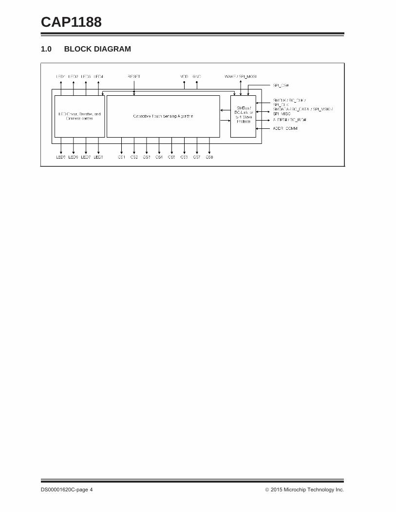
2015 Microchip Technology Inc. DS00001620C-page 1 General Description The CAP1188, which incorporates RightTouch ® tech- nology, is a multiple channel Capacitive Touch sensor with multiple power LED drivers. It contains eight (8) individual capacitive touch sensor inputs with program- mable sensitivity for use in touch sensor applications. Each sensor input automatically recalibrates to com- pensate for gradual environmental changes. The CAP1188 also contains eight (8) LED drivers that offer full-on / off, variable rate blinking, dimness con- trols, and breathing. Each of the LED drivers may be linked to one of the sensor inputs to be actuated when a touch is detected. As well, each LED driver may be individually controlled via a host controller. The CAP1188 includes Multiple Pattern Touch recogni- tion that allows the user to select a specific set of but- tons to be touched simultaneously. If this pattern is detected, then a status bit is set and an interrupt gen- erated. Additionally, the CAP1188 includes circuitry and sup- port for enhanced sensor proximity detection. The CAP1188 offers multiple power states operating at low quiescent currents. In the Standby state of opera- tion, one or more capacitive touch sensor inputs are active and all LEDs may be used. If a touch is detected, it will wake the system using the WAKE/SPI_MOSI pin. Deep Sleep is the lowest power state available, draw- ing 5uA (typical) of current. In this state, no sensor inputs are active. Driving the WAKE/SPI_MOSI pin or communications will wake the device. Applications • Desktop and Notebook PCs • LCD Monitors • Consumer Electronics • Appliances Features • Eight (8) Capacitive Touch Sensor Inputs - Programmable sensitivity - Automatic recalibration - Individual thresholds for each button • Proximity Detection • Multiple Button Pattern Detection • Calibrates for Parasitic Capacitance • Analog Filtering for System Noise Sources • Press and Hold feature for Volume-like Applica- tions • Multiple Communication Interfaces - SMBus / I 2 C compliant interface - SPI communications - Pin selectable communications protocol and multiple slave addresses (SMBus / I 2 C only) • Low Power Operation - 5uA quiescent current in Deep Sleep - 50uA quiescent current in Standby (1 sensor input monitored) - Samples one or more channels in Standby • Eight (8) LED Driver Outputs - Open Drain or Push-Pull - Programmable blink, breathe, and dimness controls - Can be linked to Capacitive Touch Sensor inputs • Dedicated Wake output flags touches in low power state • System RESET pin • Available in 24-pin 4mm x 4mm RoHS compliant QFN package CAP1188 8 Channel Capacitive Touch Sensor with 8 LED Drivers
Transcript of CAP1188 CAP1088 CAP1188-1-CP-TR Microchip Technology …

2015 Microchip Technology Inc. DS00001620C-page 1
General DescriptionThe CAP1188, which incorporates RightTouch® tech-nology, is a multiple channel Capacitive Touch sensorwith multiple power LED drivers. It contains eight (8)individual capacitive touch sensor inputs with program-mable sensitivity for use in touch sensor applications.Each sensor input automatically recalibrates to com-pensate for gradual environmental changes.
The CAP1188 also contains eight (8) LED drivers thatoffer full-on / off, variable rate blinking, dimness con-trols, and breathing. Each of the LED drivers may belinked to one of the sensor inputs to be actuated whena touch is detected. As well, each LED driver may beindividually controlled via a host controller.
The CAP1188 includes Multiple Pattern Touch recogni-tion that allows the user to select a specific set of but-tons to be touched simultaneously. If this pattern isdetected, then a status bit is set and an interrupt gen-erated.
Additionally, the CAP1188 includes circuitry and sup-port for enhanced sensor proximity detection.
The CAP1188 offers multiple power states operating atlow quiescent currents. In the Standby state of opera-tion, one or more capacitive touch sensor inputs areactive and all LEDs may be used. If a touch is detected,it will wake the system using the WAKE/SPI_MOSI pin.
Deep Sleep is the lowest power state available, draw-ing 5uA (typical) of current. In this state, no sensorinputs are active. Driving the WAKE/SPI_MOSI pin orcommunications will wake the device.
Applications• Desktop and Notebook PCs• LCD Monitors• Consumer Electronics• Appliances
Features• Eight (8) Capacitive Touch Sensor Inputs
- Programmable sensitivity- Automatic recalibration - Individual thresholds for each button
• Proximity Detection• Multiple Button Pattern Detection• Calibrates for Parasitic Capacitance• Analog Filtering for System Noise Sources• Press and Hold feature for Volume-like Applica-
tions• Multiple Communication Interfaces
- SMBus / I2C compliant interface- SPI communications- Pin selectable communications protocol and
multiple slave addresses (SMBus / I2C only)• Low Power Operation
- 5uA quiescent current in Deep Sleep- 50uA quiescent current in Standby (1 sensor
input monitored)- Samples one or more channels in Standby
• Eight (8) LED Driver Outputs- Open Drain or Push-Pull - Programmable blink, breathe, and dimness
controls- Can be linked to Capacitive Touch Sensor
inputs• Dedicated Wake output flags touches in low
power state • System RESET pin • Available in 24-pin 4mm x 4mm RoHS compliant
QFN package
CAP11888 Channel Capacitive Touch Sensor with 8 LED Drivers

CAP1188
DS00001620C-page 2 2015 Microchip Technology Inc.
TO OUR VALUED CUSTOMERSIt is our intention to provide our valued customers with the best documentation possible to ensure successful use of your Microchipproducts. To this end, we will continue to improve our publications to better suit your needs. Our publications will be refined andenhanced as new volumes and updates are introduced. If you have any questions or comments regarding this publication, please contact the Marketing Communications Department viaE-mail at [email protected]. We welcome your feedback.
Most Current Data SheetTo obtain the most up-to-date version of this data sheet, please register at our Worldwide Web site at:
http://www.microchip.comYou can determine the version of a data sheet by examining its literature number found on the bottom outside corner of any page. The last character of the literature number is the version number, (e.g., DS30000000A is version A of document DS30000000).
ErrataAn errata sheet, describing minor operational differences from the data sheet and recommended workarounds, may exist for cur-rent devices. As device/documentation issues become known to us, we will publish an errata sheet. The errata will specify therevision of silicon and revision of document to which it applies.To determine if an errata sheet exists for a particular device, please check with one of the following:• Microchip’s Worldwide Web site; http://www.microchip.com• Your local Microchip sales office (see last page)When contacting a sales office, please specify which device, revision of silicon and data sheet (include -literature number) you areusing.
Customer Notification SystemRegister on our web site at www.microchip.com to receive the most current information on all of our products.
2015 Microchip Technology Inc. DS00001620C-page 3
CAP1188Table of Contents1.0 Block Diagram ................................................................................................................................................................................. 42.0 Pin Description ................................................................................................................................................................................ 53.0 Electrical Specifications .................................................................................................................................................................. 94.0 Communications ........................................................................................................................................................................... 125.0 General Description ...................................................................................................................................................................... 236.0 Register Description ...................................................................................................................................................................... 297.0 Package Information ..................................................................................................................................................................... 67Appendix A: Device Delta ................................................................................................................................................................... 72Appendix B: Data Sheet Revision History ........................................................................................................................................... 74The Microchip Web Site ...................................................................................................................................................................... 76Customer Change Notification Service ............................................................................................................................................... 76Customer Support ............................................................................................................................................................................... 76Product Identification System ............................................................................................................................................................. 77
CAP1188
DS00001620C-page 4 2015 Microchip Technology Inc.
1.0 BLOCK DIAGRAM
2015 Microchip Technology Inc. DS00001620C-page 5
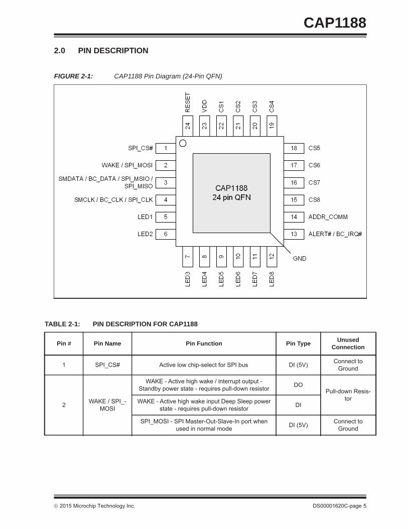
CAP11882.0 PIN DESCRIPTION
FIGURE 2-1: CAP1188 Pin Diagram (24-Pin QFN)
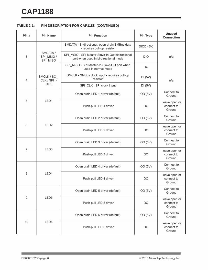
TABLE 2-1: PIN DESCRIPTION FOR CAP1188
Pin # Pin Name Pin Function Pin Type Unused Connection
1 SPI_CS# Active low chip-select for SPI bus DI (5V) Connect to Ground
2 WAKE / SPI_-MOSI
WAKE - Active high wake / interrupt output - Standby power state - requires pull-down resistor DO
Pull-down Resis-torWAKE - Active high wake input Deep Sleep power
state - requires pull-down resistor DI
SPI_MOSI - SPI Master-Out-Slave-In port when used in normal mode DI (5V) Connect to
Ground
CAP1188
DS00001620C-page 6 2015 Microchip Technology Inc.
3SMDATA /
SPI_MSIO / SPI_MISO
SMDATA - Bi-directional, open-drain SMBus data - requires pull-up resistor DIOD (5V)
n/aSPI_MSIO - SPI Master-Slave-In-Out bidirectional port when used in bi-directional mode DIO
SPI_MISO - SPI Master-In-Slave-Out port when used in normal mode DO
4SMCLK / BC_-
CLK / SPI_-CLK
SMCLK - SMBus clock input - requires pull-up resistor DI (5V)
n/a
SPI_CLK - SPI clock input DI (5V)
5 LED1
Open drain LED 1 driver (default) OD (5V) Connect to Ground
Push-pull LED 1 driver DO leave open or
connect to Ground
6 LED2
Open drain LED 2 driver (default) OD (5V) Connect to Ground
Push-pull LED 2 driver DO leave open or
connect to Ground
7 LED3
Open drain LED 3 driver (default) OD (5V) Connect to Ground
Push-pull LED 3 driver DO leave open or
connect to Ground
8 LED4
Open drain LED 4 driver (default) OD (5V) Connect to Ground
Push-pull LED 4 driver DO leave open or
connect to Ground
9 LED5
Open drain LED 5 driver (default) OD (5V) Connect to Ground
Push-pull LED 5 driver DO leave open or
connect to Ground
10 LED6
Open drain LED 6 driver (default) OD (5V) Connect to Ground
Push-pull LED 6 driver DO leave open or
connect to Ground
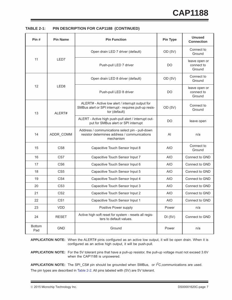
TABLE 2-1: PIN DESCRIPTION FOR CAP1188 (CONTINUED)
Pin # Pin Name Pin Function Pin Type Unused Connection
2015 Microchip Technology Inc. DS00001620C-page 7
CAP1188
APPLICATION NOTE: When the ALERT# pinis configured as an active low output, it will be open drain. When it isconfigured as an active high output, it will be push-pull.
APPLICATION NOTE: For the 5V tolerant pins that have a pull-up resistor, the pull-up voltage must not exceed 3.6Vwhen the CAP1188 is unpowered.
APPLICATION NOTE: The SPI_CS# pin should be grounded when SMBus, or I2C,communications are used.
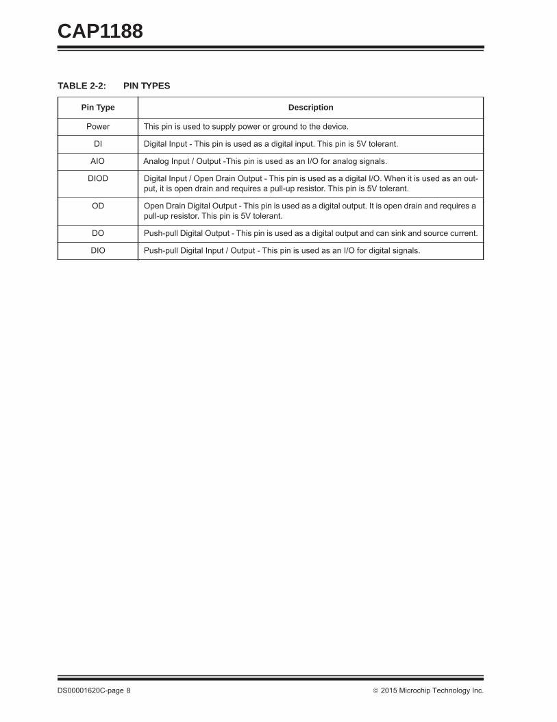
The pin types are described in Table 2-2. All pins labeled with (5V) are 5V tolerant.
11 LED7
Open drain LED 7 driver (default) OD (5V) Connect to Ground
Push-pull LED 7 driver DO leave open or
connect to Ground
12 LED8
Open drain LED 8 driver (default) OD (5V) Connect to Ground
Push-pull LED 8 driver DO leave open or
connect to Ground
13 ALERT#
ALERT# - Active low alert / interrupt output for SMBus alert or SPI interrupt - requires pull-up resis-
tor (default)OD (5V) Connect to
Ground
ALERT - Active high push-pull alert / interrupt out-put for SMBus alert or SPI interrupt DO leave open
14 ADDR_COMMAddress / communications select pin - pull-down
resistor determines address / communications mechanism
AI n/a
15 CS8 Capacitive Touch Sensor Input 8 AIO Connect to Ground
16 CS7 Capacitive Touch Sensor Input 7 AIO Connect to GND
17 CS6 Capacitive Touch Sensor Input 6 AIO Connect to GND
18 CS5 Capacitive Touch Sensor Input 5 AIO Connect to GND
19 CS4 Capacitive Touch Sensor Input 4 AIO Connect to GND
20 CS3 Capacitive Touch Sensor Input 3 AIO Connect to GND
21 CS2 Capacitive Touch Sensor Input 2 AIO Connect to GND
22 CS1 Capacitive Touch Sensor Input 1 AIO Connect to GND
23 VDD Positive Power supply Power n/a
24 RESET Active high soft reset for system - resets all regis-ters to default values. DI (5V) Connect to GND
Bottom Pad GND Ground Power n/a
TABLE 2-1: PIN DESCRIPTION FOR CAP1188 (CONTINUED)
Pin # Pin Name Pin Function Pin Type Unused Connection
CAP1188
DS00001620C-page 8 2015 Microchip Technology Inc.
TABLE 2-2: PIN TYPES
Pin Type Description
Power This pin is used to supply power or ground to the device.
DI Digital Input - This pin is used as a digital input. This pin is 5V tolerant.
AIO Analog Input / Output -This pin is used as an I/O for analog signals.
DIOD Digital Input / Open Drain Output - This pin is used as a digital I/O. When it is used as an out-put, it is open drain and requires a pull-up resistor. This pin is 5V tolerant.
OD Open Drain Digital Output - This pin is used as a digital output. It is open drain and requires a pull-up resistor. This pin is 5V tolerant.
DO Push-pull Digital Output - This pin is used as a digital output and can sink and source current.
DIO Push-pull Digital Input / Output - This pin is used as an I/O for digital signals.
2015 Microchip Technology Inc. DS00001620C-page 9
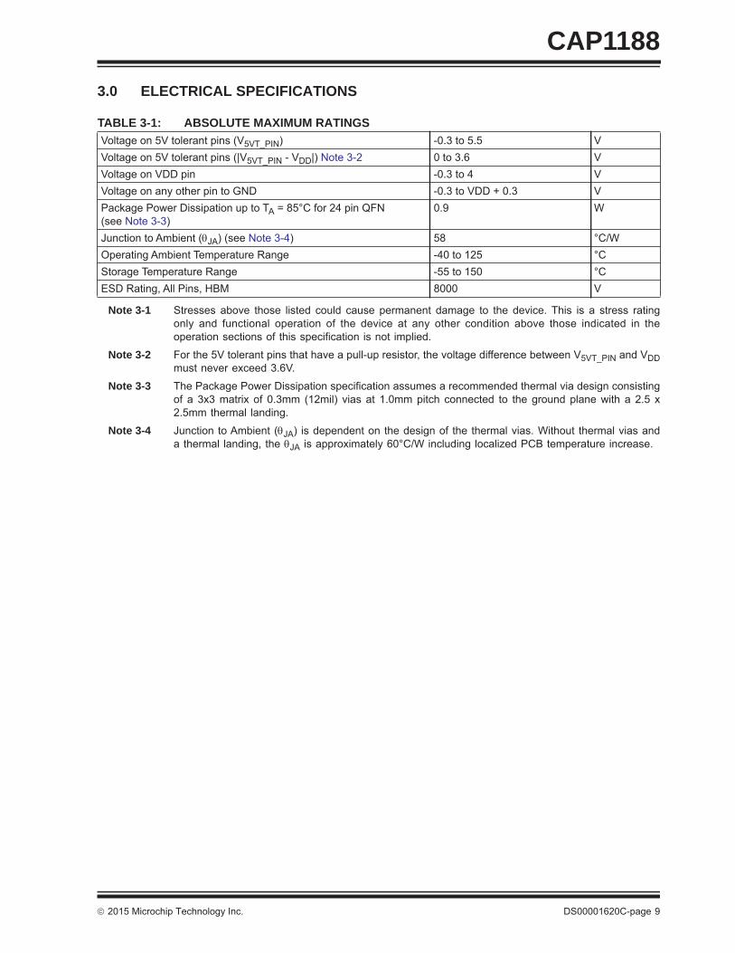
CAP11883.0 ELECTRICAL SPECIFICATIONS
Note 3-1 Stresses above those listed could cause permanent damage to the device. This is a stress ratingonly and functional operation of the device at any other condition above those indicated in theoperation sections of this specification is not implied.
Note 3-2 For the 5V tolerant pins that have a pull-up resistor, the voltage difference between V5VT_PIN and VDDmust never exceed 3.6V.
Note 3-3 The Package Power Dissipation specification assumes a recommended thermal via design consistingof a 3x3 matrix of 0.3mm (12mil) vias at 1.0mm pitch connected to the ground plane with a 2.5 x2.5mm thermal landing.
Note 3-4 Junction to Ambient (JA) is dependent on the design of the thermal vias. Without thermal vias anda thermal landing, the JA is approximately 60°C/W including localized PCB temperature increase.
TABLE 3-1: ABSOLUTE MAXIMUM RATINGSVoltage on 5V tolerant pins (V5VT_PIN) -0.3 to 5.5 VVoltage on 5V tolerant pins (|V5VT_PIN - VDD|) Note 3-2 0 to 3.6 VVoltage on VDD pin -0.3 to 4 VVoltage on any other pin to GND -0.3 to VDD + 0.3 VPackage Power Dissipation up to TA = 85°C for 24 pin QFN(see Note 3-3)
0.9 W
Junction to Ambient (JA) (see Note 3-4) 58 °C/WOperating Ambient Temperature Range -40 to 125 °CStorage Temperature Range -55 to 150 °CESD Rating, All Pins, HBM 8000 V
CAP1188
DS00001620C-page 10 2015 Microchip Technology Inc.
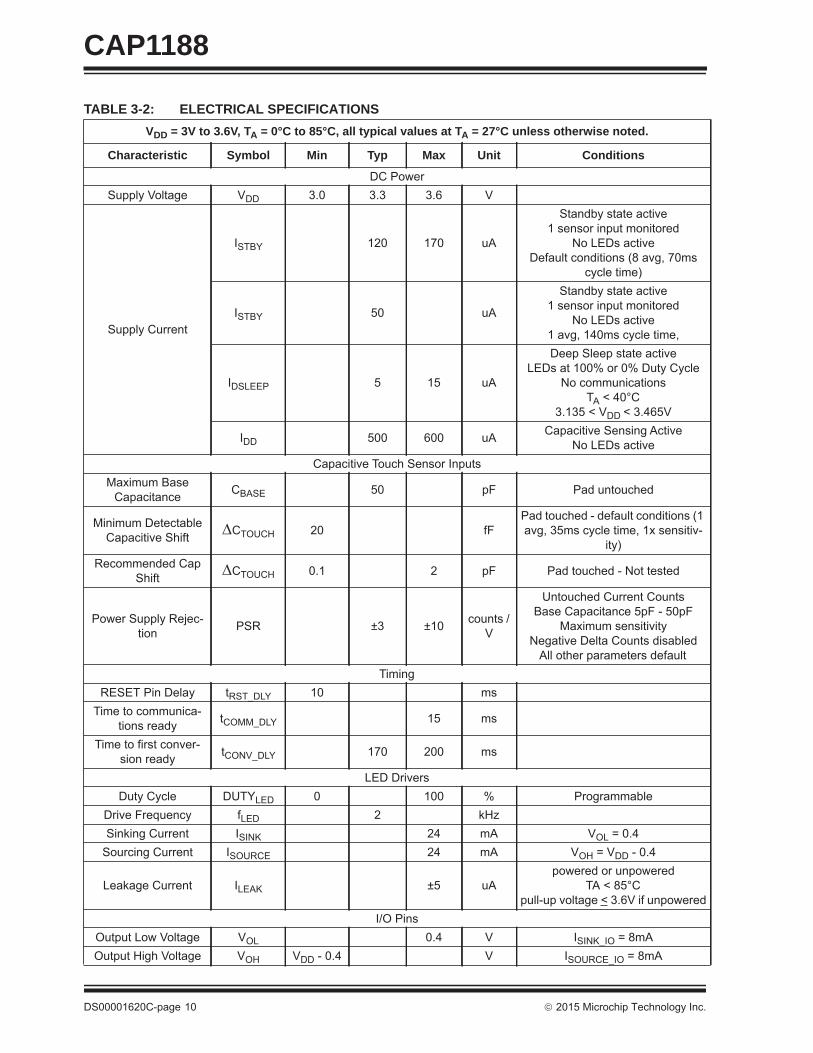
TABLE 3-2: ELECTRICAL SPECIFICATIONS
VDD = 3V to 3.6V, TA = 0°C to 85°C, all typical values at TA = 27°C unless otherwise noted.
Characteristic Symbol Min Typ Max Unit Conditions
DC PowerSupply Voltage VDD 3.0 3.3 3.6 V
Supply Current
ISTBY 120 170 uA
Standby state active 1 sensor input monitored
No LEDs activeDefault conditions (8 avg, 70ms
cycle time)
ISTBY 50 uA
Standby state active1 sensor input monitored
No LEDs active1 avg, 140ms cycle time,
IDSLEEP 5 15 uA
Deep Sleep state activeLEDs at 100% or 0% Duty Cycle
No communicationsTA < 40°C
3.135 < VDD < 3.465V
IDD 500 600 uA Capacitive Sensing ActiveNo LEDs active
Capacitive Touch Sensor InputsMaximum Base
Capacitance CBASE 50 pF Pad untouched
Minimum Detectable Capacitive Shift CTOUCH 20 fF
Pad touched - default conditions (1 avg, 35ms cycle time, 1x sensitiv-
ity) Recommended Cap
Shift CTOUCH 0.1 2 pF Pad touched - Not tested
Power Supply Rejec-tion PSR ±3 ±10 counts /
V
Untouched Current Counts Base Capacitance 5pF - 50pF
Maximum sensitivityNegative Delta Counts disabled
All other parameters defaultTiming
RESET Pin Delay tRST_DLY 10 msTime to communica-
tions ready tCOMM_DLY 15 ms
Time to first conver-sion ready tCONV_DLY 170 200 ms
LED Drivers Duty Cycle DUTYLED 0 100 % Programmable
Drive Frequency fLED 2 kHzSinking Current ISINK 24 mA VOL = 0.4
Sourcing Current ISOURCE 24 mA VOH = VDD - 0.4
Leakage Current ILEAK ±5 uApowered or unpowered
TA < 85°Cpull-up voltage < 3.6V if unpowered
I/O PinsOutput Low Voltage VOL 0.4 V ISINK_IO = 8mAOutput High Voltage VOH VDD - 0.4 V ISOURCE_IO = 8mA
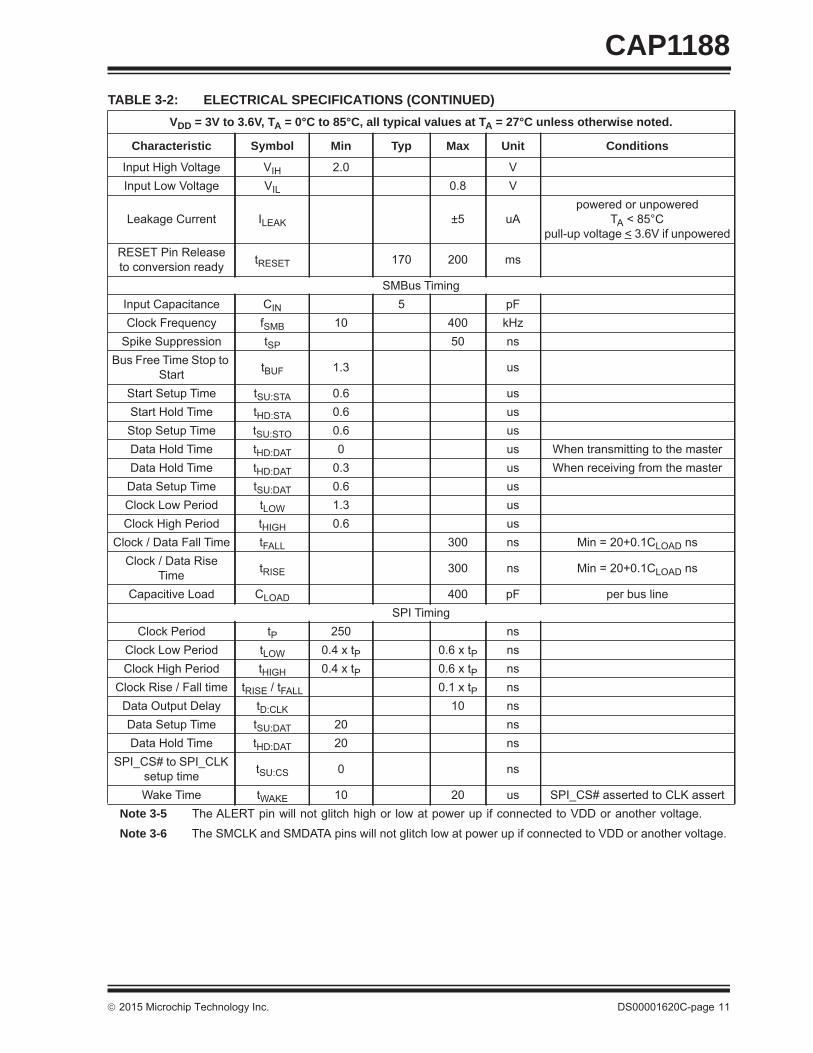
2015 Microchip Technology Inc. DS00001620C-page 11
CAP1188
Note 3-5 The ALERT pin will not glitch high or low at power up if connected to VDD or another voltage.
Note 3-6 The SMCLK and SMDATA pins will not glitch low at power up if connected to VDD or another voltage.
Input High Voltage VIH 2.0 VInput Low Voltage VIL 0.8 V
Leakage Current ILEAK ±5 uApowered or unpowered
TA < 85°Cpull-up voltage < 3.6V if unpowered
RESET Pin Release to conversion ready tRESET 170 200 ms
SMBus TimingInput Capacitance CIN 5 pFClock Frequency fSMB 10 400 kHz
Spike Suppression tSP 50 nsBus Free Time Stop to
Start tBUF 1.3 us
Start Setup Time tSU:STA 0.6 usStart Hold Time tHD:STA 0.6 usStop Setup Time tSU:STO 0.6 usData Hold Time tHD:DAT 0 us When transmitting to the masterData Hold Time tHD:DAT 0.3 us When receiving from the master
Data Setup Time tSU:DAT 0.6 usClock Low Period tLOW 1.3 usClock High Period tHIGH 0.6 us
Clock / Data Fall Time tFALL 300 ns Min = 20+0.1CLOAD nsClock / Data Rise
Time tRISE 300 ns Min = 20+0.1CLOAD ns
Capacitive Load CLOAD 400 pF per bus lineSPI Timing
Clock Period tP 250 nsClock Low Period tLOW 0.4 x tP 0.6 x tP nsClock High Period tHIGH 0.4 x tP 0.6 x tP ns
Clock Rise / Fall time tRISE / tFALL 0.1 x tP nsData Output Delay tD:CLK 10 nsData Setup Time tSU:DAT 20 nsData Hold Time tHD:DAT 20 ns
SPI_CS# to SPI_CLK setup time tSU:CS 0 ns
Wake Time tWAKE 10 20 us SPI_CS# asserted to CLK assert
TABLE 3-2: ELECTRICAL SPECIFICATIONS (CONTINUED) VDD = 3V to 3.6V, TA = 0°C to 85°C, all typical values at TA = 27°C unless otherwise noted.
Characteristic Symbol Min Typ Max Unit Conditions
CAP1188
DS00001620C-page 12 2015 Microchip Technology Inc.
4.0 COMMUNICATIONS
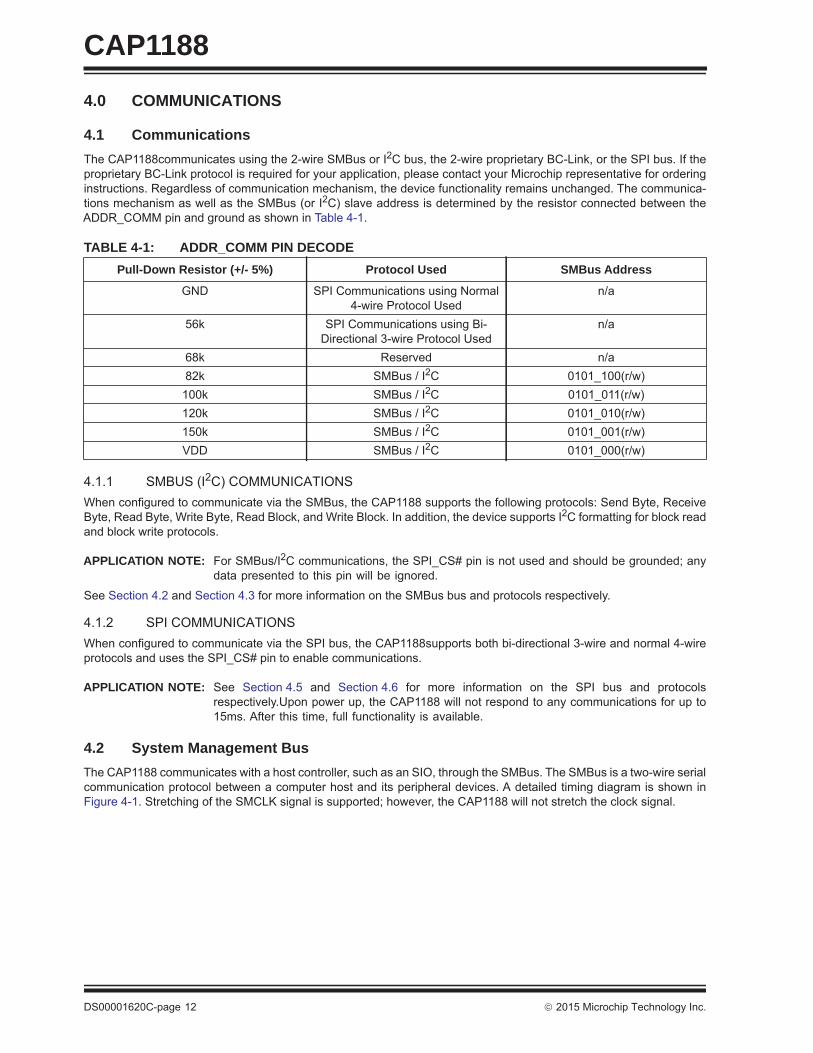
4.1 CommunicationsThe CAP1188communicates using the 2-wire SMBus or I2C bus, the 2-wire proprietary BC-Link, or the SPI bus. If theproprietary BC-Link protocol is required for your application, please contact your Microchip representative for orderinginstructions. Regardless of communication mechanism, the device functionality remains unchanged. The communica-tions mechanism as well as the SMBus (or I2C) slave address is determined by the resistor connected between theADDR_COMM pin and ground as shown in Table 4-1.
4.1.1 SMBUS (I2C) COMMUNICATIONSWhen configured to communicate via the SMBus, the CAP1188 supports the following protocols: Send Byte, ReceiveByte, Read Byte, Write Byte, Read Block, and Write Block. In addition, the device supports I2C formatting for block readand block write protocols.
APPLICATION NOTE: For SMBus/I2C communications, the SPI_CS# pin is not used and should be grounded; anydata presented to this pin will be ignored.
See Section 4.2 and Section 4.3 for more information on the SMBus bus and protocols respectively.
4.1.2 SPI COMMUNICATIONSWhen configured to communicate via the SPI bus, the CAP1188supports both bi-directional 3-wire and normal 4-wireprotocols and uses the SPI_CS# pin to enable communications.
APPLICATION NOTE: See Section 4.5 and Section 4.6 for more information on the SPI bus and protocolsrespectively.Upon power up, the CAP1188 will not respond to any communications for up to15ms. After this time, full functionality is available.
4.2 System Management BusThe CAP1188 communicates with a host controller, such as an SIO, through the SMBus. The SMBus is a two-wire serialcommunication protocol between a computer host and its peripheral devices. A detailed timing diagram is shown inFigure 4-1. Stretching of the SMCLK signal is supported; however, the CAP1188 will not stretch the clock signal.
TABLE 4-1: ADDR_COMM PIN DECODEPull-Down Resistor (+/- 5%) Protocol Used SMBus Address
GND SPI Communications using Normal 4-wire Protocol Used
n/a
56k SPI Communications using Bi-Directional 3-wire Protocol Used
n/a
68k Reserved n/a82k SMBus / I2C 0101_100(r/w)
100k SMBus / I2C 0101_011(r/w)120k SMBus / I2C 0101_010(r/w)150k SMBus / I2C 0101_001(r/w)VDD SMBus / I2C 0101_000(r/w)
2015 Microchip Technology Inc. DS00001620C-page 13
CAP1188
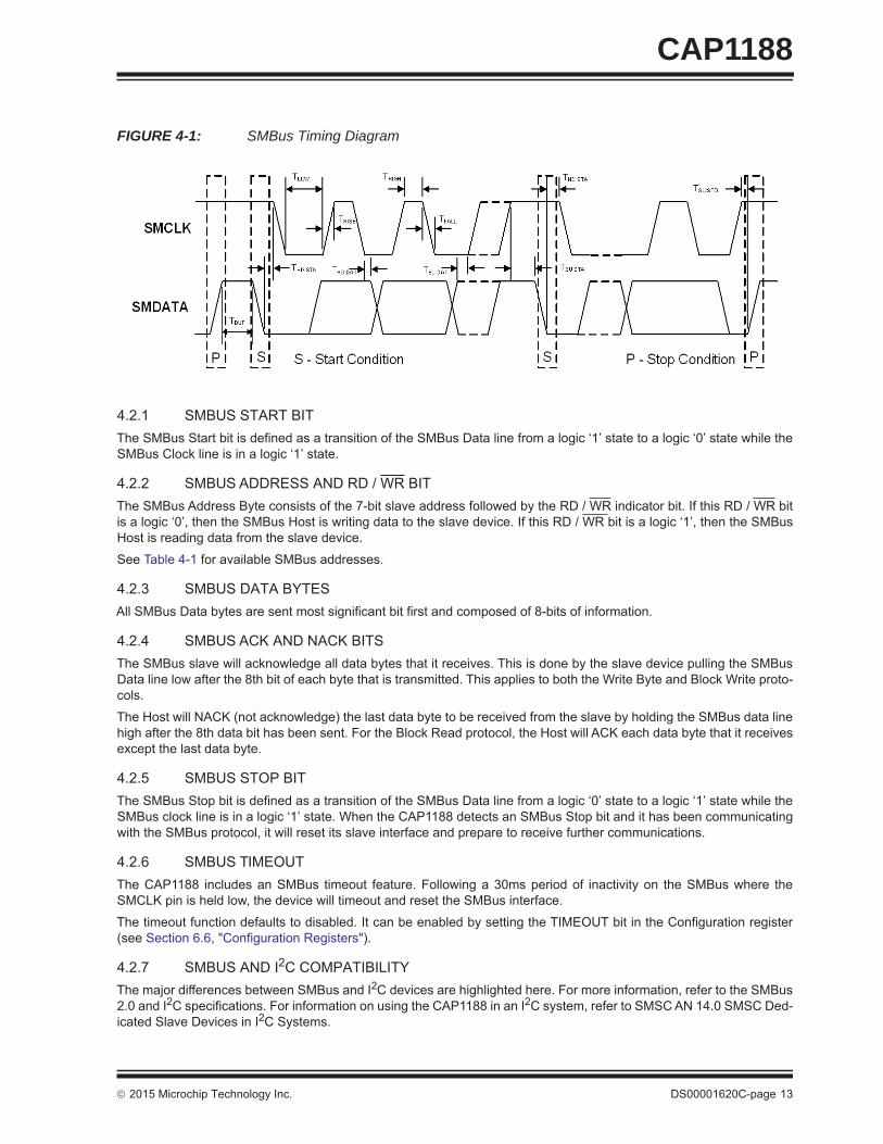
4.2.1 SMBUS START BITThe SMBus Start bit is defined as a transition of the SMBus Data line from a logic ‘1’ state to a logic ‘0’ state while theSMBus Clock line is in a logic ‘1’ state.
4.2.2 SMBUS ADDRESS AND RD / WR BITThe SMBus Address Byte consists of the 7-bit slave address followed by the RD / WR indicator bit. If this RD / WR bitis a logic ‘0’, then the SMBus Host is writing data to the slave device. If this RD / WR bit is a logic ‘1’, then the SMBusHost is reading data from the slave device.
See Table 4-1 for available SMBus addresses.
4.2.3 SMBUS DATA BYTESAll SMBus Data bytes are sent most significant bit first and composed of 8-bits of information.
4.2.4 SMBUS ACK AND NACK BITSThe SMBus slave will acknowledge all data bytes that it receives. This is done by the slave device pulling the SMBusData line low after the 8th bit of each byte that is transmitted. This applies to both the Write Byte and Block Write proto-cols.
The Host will NACK (not acknowledge) the last data byte to be received from the slave by holding the SMBus data linehigh after the 8th data bit has been sent. For the Block Read protocol, the Host will ACK each data byte that it receivesexcept the last data byte.
4.2.5 SMBUS STOP BITThe SMBus Stop bit is defined as a transition of the SMBus Data line from a logic ‘0’ state to a logic ‘1’ state while theSMBus clock line is in a logic ‘1’ state. When the CAP1188 detects an SMBus Stop bit and it has been communicatingwith the SMBus protocol, it will reset its slave interface and prepare to receive further communications.
4.2.6 SMBUS TIMEOUTThe CAP1188 includes an SMBus timeout feature. Following a 30ms period of inactivity on the SMBus where theSMCLK pin is held low, the device will timeout and reset the SMBus interface.
The timeout function defaults to disabled. It can be enabled by setting the TIMEOUT bit in the Configuration register(see Section 6.6, "Configuration Registers").
4.2.7 SMBUS AND I2C COMPATIBILITYThe major differences between SMBus and I2C devices are highlighted here. For more information, refer to the SMBus2.0 and I2C specifications. For information on using the CAP1188 in an I2C system, refer to SMSC AN 14.0 SMSC Ded-icated Slave Devices in I2C Systems.
FIGURE 4-1: SMBus Timing Diagram
CAP1188
DS00001620C-page 14 2015 Microchip Technology Inc.
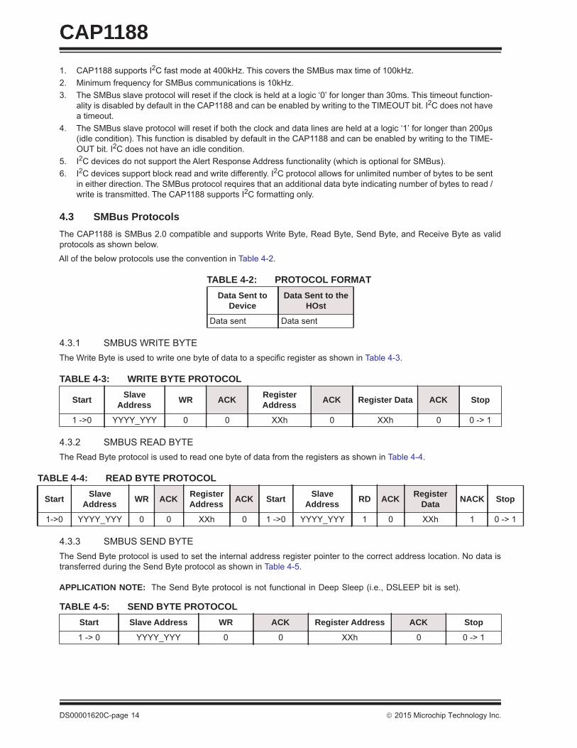
1. CAP1188 supports I2C fast mode at 400kHz. This covers the SMBus max time of 100kHz.2. Minimum frequency for SMBus communications is 10kHz.3. The SMBus slave protocol will reset if the clock is held at a logic ‘0’ for longer than 30ms. This timeout function-
ality is disabled by default in the CAP1188 and can be enabled by writing to the TIMEOUT bit. I2C does not havea timeout.
4. The SMBus slave protocol will reset if both the clock and data lines are held at a logic ‘1’ for longer than 200μs(idle condition). This function is disabled by default in the CAP1188 and can be enabled by writing to the TIME-OUT bit. I2C does not have an idle condition.
5. I2C devices do not support the Alert Response Address functionality (which is optional for SMBus). 6. I2C devices support block read and write differently. I2C protocol allows for unlimited number of bytes to be sent
in either direction. The SMBus protocol requires that an additional data byte indicating number of bytes to read /write is transmitted. The CAP1188 supports I2C formatting only.
4.3 SMBus Protocols The CAP1188 is SMBus 2.0 compatible and supports Write Byte, Read Byte, Send Byte, and Receive Byte as validprotocols as shown below.
All of the below protocols use the convention in Table 4-2.
4.3.1 SMBUS WRITE BYTEThe Write Byte is used to write one byte of data to a specific register as shown in Table 4-3.
4.3.2 SMBUS READ BYTEThe Read Byte protocol is used to read one byte of data from the registers as shown in Table 4-4.
4.3.3 SMBUS SEND BYTEThe Send Byte protocol is used to set the internal address register pointer to the correct address location. No data istransferred during the Send Byte protocol as shown in Table 4-5.
APPLICATION NOTE: The Send Byte protocol is not functional in Deep Sleep (i.e., DSLEEP bit is set).
TABLE 4-2: PROTOCOL FORMATData Sent to
DeviceData Sent to the
HOst
Data sent Data sent
TABLE 4-3: WRITE BYTE PROTOCOL
Start Slave Address WR ACK Register
Address ACK Register Data ACK Stop
1 ->0 YYYY_YYY 0 0 XXh 0 XXh 0 0 -> 1
TABLE 4-4: READ BYTE PROTOCOL
Start Slave Address WR ACK Register
Address ACK Start Slave Address RD ACK Register
Data NACK Stop
1->0 YYYY_YYY 0 0 XXh 0 1 ->0 YYYY_YYY 1 0 XXh 1 0 -> 1
TABLE 4-5: SEND BYTE PROTOCOLStart Slave Address WR ACK Register Address ACK Stop
1 -> 0 YYYY_YYY 0 0 XXh 0 0 -> 1
2015 Microchip Technology Inc. DS00001620C-page 15
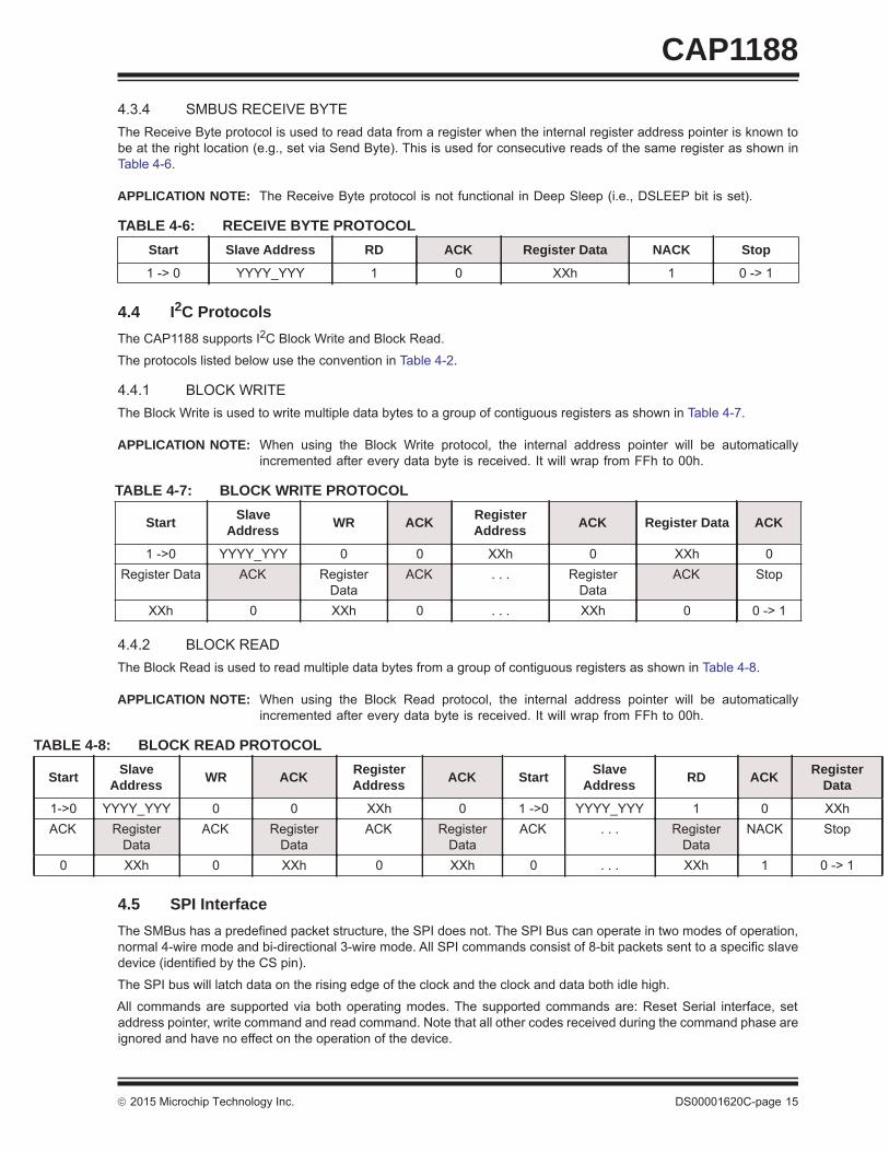
CAP11884.3.4 SMBUS RECEIVE BYTEThe Receive Byte protocol is used to read data from a register when the internal register address pointer is known tobe at the right location (e.g., set via Send Byte). This is used for consecutive reads of the same register as shown inTable 4-6.
APPLICATION NOTE: The Receive Byte protocol is not functional in Deep Sleep (i.e., DSLEEP bit is set).
4.4 I2C ProtocolsThe CAP1188 supports I2C Block Write and Block Read.
The protocols listed below use the convention in Table 4-2.
4.4.1 BLOCK WRITE The Block Write is used to write multiple data bytes to a group of contiguous registers as shown in Table 4-7.
APPLICATION NOTE: When using the Block Write protocol, the internal address pointer will be automaticallyincremented after every data byte is received. It will wrap from FFh to 00h.
4.4.2 BLOCK READ The Block Read is used to read multiple data bytes from a group of contiguous registers as shown in Table 4-8.
APPLICATION NOTE: When using the Block Read protocol, the internal address pointer will be automaticallyincremented after every data byte is received. It will wrap from FFh to 00h.
4.5 SPI InterfaceThe SMBus has a predefined packet structure, the SPI does not. The SPI Bus can operate in two modes of operation,normal 4-wire mode and bi-directional 3-wire mode. All SPI commands consist of 8-bit packets sent to a specific slavedevice (identified by the CS pin).
The SPI bus will latch data on the rising edge of the clock and the clock and data both idle high.
All commands are supported via both operating modes. The supported commands are: Reset Serial interface, setaddress pointer, write command and read command. Note that all other codes received during the command phase areignored and have no effect on the operation of the device.
TABLE 4-6: RECEIVE BYTE PROTOCOLStart Slave Address RD ACK Register Data NACK Stop
1 -> 0 YYYY_YYY 1 0 XXh 1 0 -> 1
TABLE 4-7: BLOCK WRITE PROTOCOL
Start Slave Address WR ACK Register
Address ACK Register Data ACK
1 ->0 YYYY_YYY 0 0 XXh 0 XXh 0Register Data ACK Register
DataACK . . . Register
DataACK Stop
XXh 0 XXh 0 . . . XXh 0 0 -> 1
TABLE 4-8: BLOCK READ PROTOCOL
Start Slave Address WR ACK Register
Address ACK Start Slave Address RD ACK Register
Data
1->0 YYYY_YYY 0 0 XXh 0 1 ->0 YYYY_YYY 1 0 XXhACK Register
DataACK Register
DataACK Register
DataACK . . . Register
DataNACK Stop
0 XXh 0 XXh 0 XXh 0 . . . XXh 1 0 -> 1
CAP1188
DS00001620C-page 16 2015 Microchip Technology Inc.
4.5.1 SPI NORMAL MODEThe SPI Bus can operate in two modes of operation, normal and bi-directional mode. In the normal mode of operation,there are dedicated input and output data lines. The host communicates by sending a command along the CAP1188SPI_MOSI data line and reading data on the SPI_MISO data line. Both communications occur simultaneously whichallows for larger throughput of data transactions.
All basic transfers consist of two 8 bit transactions from the Master device while the slave device is simultaneously send-ing data at the current address pointer value.
Data writes consist of two or more 8-bit transactions. The host sends a specific write command followed by the data towrite the address pointer. Data reads consist of one or more 8-bit transactions. The host sends the specific read datacommand and continues clocking for as many data bytes as it wishes to receive.
4.5.2 SPI BI-DIRECTIONAL MODEIn the bi-directional mode of operation, the SPI data signals are combined into the SPI_MSIO line, which is shared fordata received by the device and transmitted by the device. The protocol uses a simple handshake and turn aroundsequence for data communications based on the number of clocks transmitted during each phase.
All basic transfers consist of two 8 bit transactions. The first is an 8 bit command phase driven by the Master device.The second is by an 8 bit data phase driven by the Master for writes, and by the CAP1188 for read operations.
The auto increment feature of the address pointer allows for successive reads or writes. The address pointer will returnto 00h after reaching FFh.
4.5.3 SPI_CS# PINThe SPI Bus is a single master, multiple slave serial bus. Each slave has a dedicated CS pin (chip select) that the masterasserts low to identify that the slave is being addressed. There are no formal addressing options.
4.5.4 ADDRESS POINTERAll data writes and reads are accessed from the current address pointer. In both Bi-directional mode and Full Duplexmode, the Address pointer is automatically incremented following every read command or every write command.
The address pointer will return to 00h after reaching FFh.
4.5.5 SPI TIMEOUTThe CAP1188 does not detect any timeout conditions on the SPI bus.
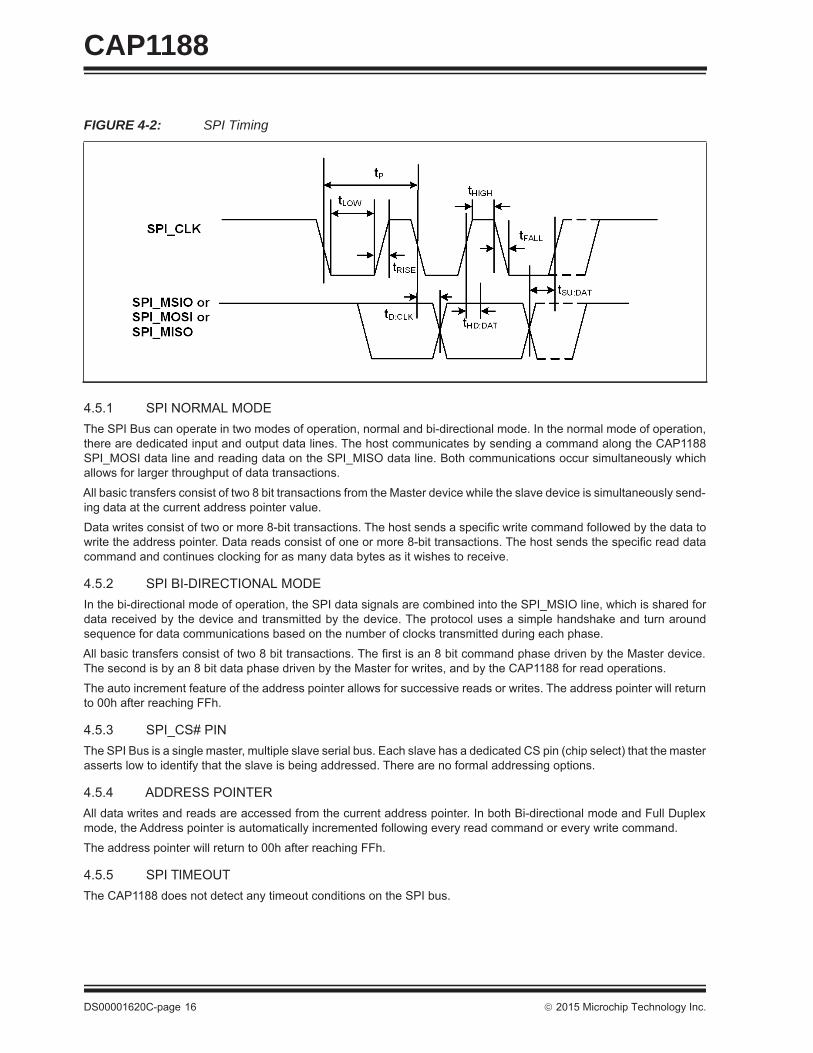
FIGURE 4-2: SPI Timing
2015 M
icrochip Technology Inc.D
S00001620C
-page 17
CA
P1188
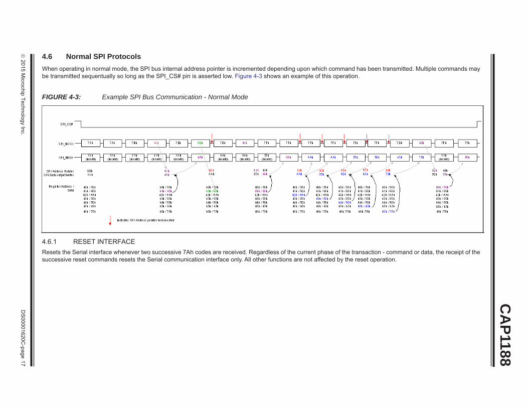
4.6 Normal SPI ProtocolsWhen operating in normal mode, the SPI bus internal address pointer is incremented depending upon which command has been transmitted. Multiple commands maybe transmitted sequentually so long as the SPI_CS# pin is asserted low. Figure 4-3 shows an example of this operation.
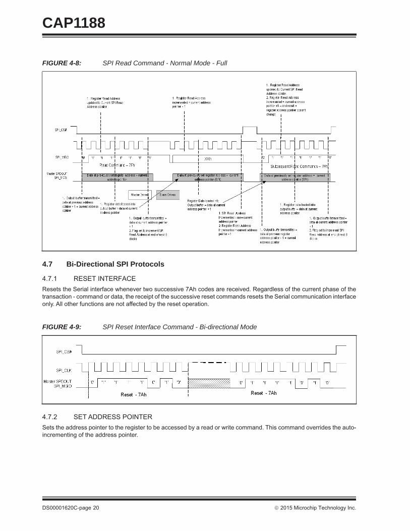
4.6.1 RESET INTERFACEResets the Serial interface whenever two successive 7Ah codes are received. Regardless of the current phase of the transaction - command or data, the receipt of thesuccessive reset commands resets the Serial communication interface only. All other functions are not affected by the reset operation.
FIGURE 4-3: Example SPI Bus Communication - Normal Mode
CAP1188
DS00001620C-page 18 2015 Microchip Technology Inc.
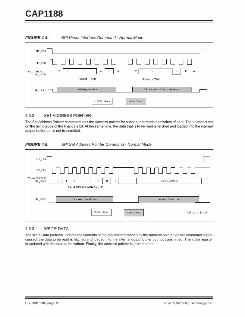
4.6.2 SET ADDRESS POINTERThe Set Address Pointer command sets the Address pointer for subsequent reads and writes of data. The pointer is seton the rising edge of the final data bit. At the same time, the data that is to be read is fetched and loaded into the internaloutput buffer but is not transmitted.
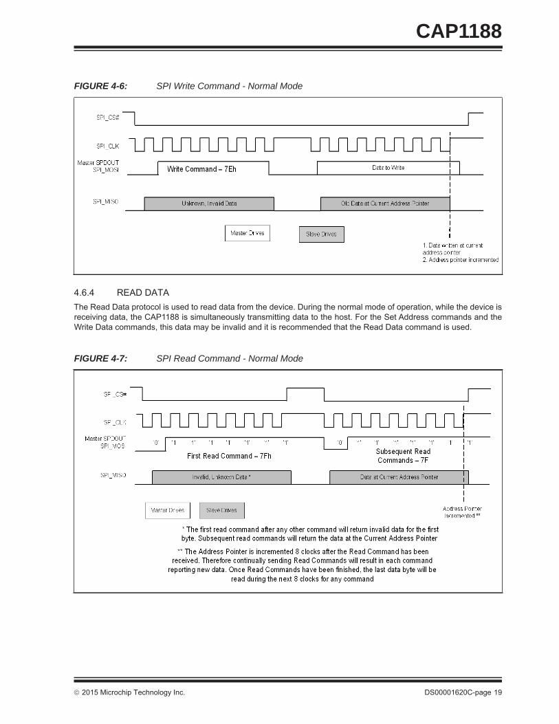
4.6.3 WRITE DATAThe Write Data protocol updates the contents of the register referenced by the address pointer. As the command is pro-cessed, the data to be read is fetched and loaded into the internal output buffer but not transmitted. Then, the registeris updated with the data to be written. Finally, the address pointer is incremented.
FIGURE 4-4: SPI Reset Interface Command - Normal Mode
FIGURE 4-5: SPI Set Address Pointer Command - Normal Mode
2015 Microchip Technology Inc. DS00001620C-page 19
CAP1188
4.6.4 READ DATAThe Read Data protocol is used to read data from the device. During the normal mode of operation, while the device isreceiving data, the CAP1188 is simultaneously transmitting data to the host. For the Set Address commands and theWrite Data commands, this data may be invalid and it is recommended that the Read Data command is used.
FIGURE 4-6: SPI Write Command - Normal Mode
FIGURE 4-7: SPI Read Command - Normal Mode
CAP1188
DS00001620C-page 20 2015 Microchip Technology Inc.
4.7 Bi-Directional SPI Protocols
4.7.1 RESET INTERFACEResets the Serial interface whenever two successive 7Ah codes are received. Regardless of the current phase of thetransaction - command or data, the receipt of the successive reset commands resets the Serial communication interfaceonly. All other functions are not affected by the reset operation.
4.7.2 SET ADDRESS POINTERSets the address pointer to the register to be accessed by a read or write command. This command overrides the auto-incrementing of the address pointer.
FIGURE 4-8: SPI Read Command - Normal Mode - Full
FIGURE 4-9: SPI Reset Interface Command - Bi-directional Mode
2015 Microchip Technology Inc. DS00001620C-page 21
CAP1188
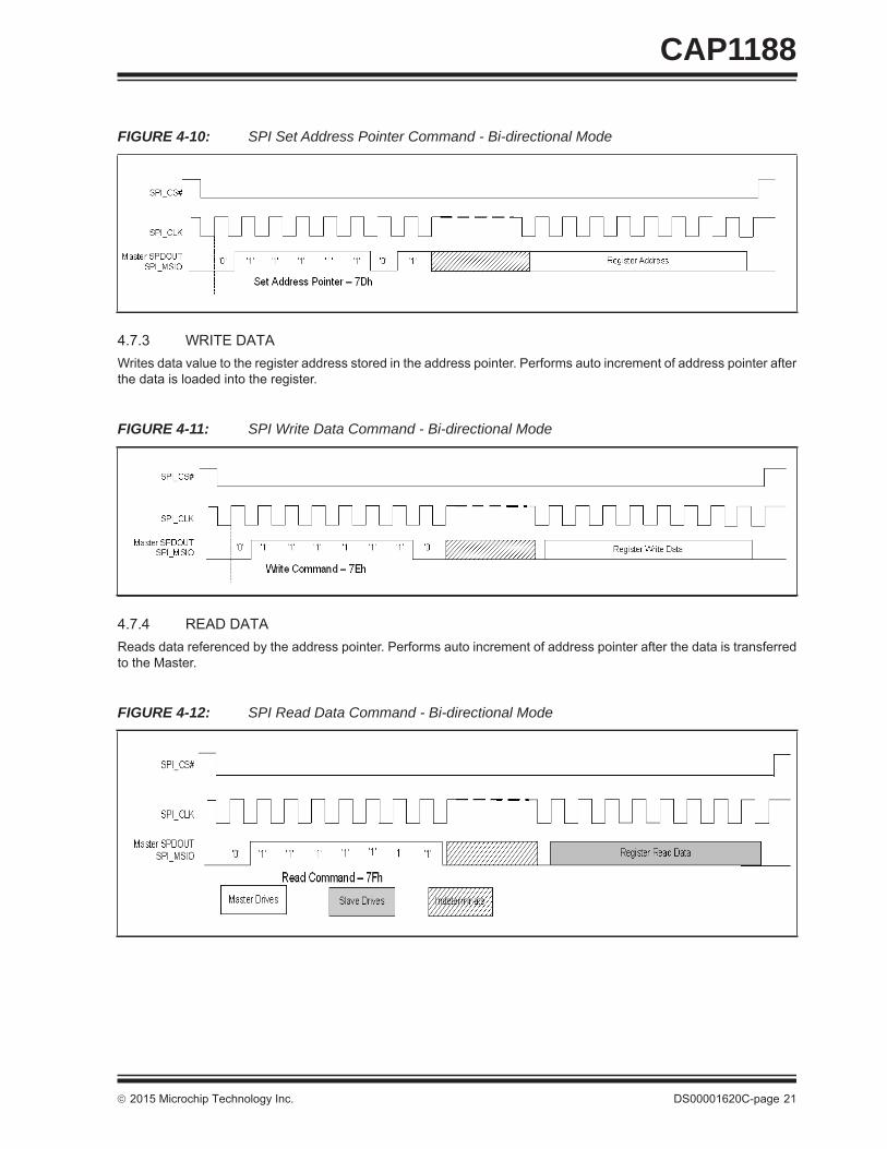
4.7.3 WRITE DATA Writes data value to the register address stored in the address pointer. Performs auto increment of address pointer afterthe data is loaded into the register.
4.7.4 READ DATAReads data referenced by the address pointer. Performs auto increment of address pointer after the data is transferredto the Master.
FIGURE 4-10: SPI Set Address Pointer Command - Bi-directional Mode
FIGURE 4-11: SPI Write Data Command - Bi-directional Mode
FIGURE 4-12: SPI Read Data Command - Bi-directional Mode
CAP1188
DS00001620C-page 22 2015 Microchip Technology Inc.
4.8 BC-Link InterfaceThe BC-Link is a proprietary bus developed to allow communication between a host controller device to a companiondevice. This device uses this serial bus to read and write registers and for interrupt processing. The interface uses adata port concept, where the base interface has an address register, data register and a control register, defined in the8051’s SFR space.
Refer to documentation for the BC-Link compatible host controller for details on how to access the CAP1188 via the BC-Link Interface.
2015 Microchip Technology Inc. DS00001620C-page 23
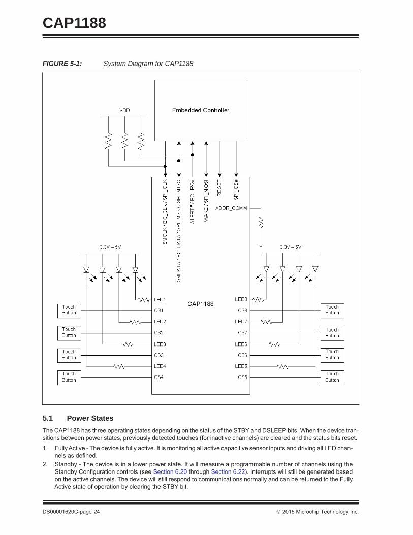
CAP11885.0 GENERAL DESCRIPTIONThe CAP1188 is a multiple channel Capacitive Touch sensor with multiple power LED drivers. It contains eight (8) indi-vidual capacitive touch sensor inputs with programmable sensitivity for use in touch sensor applications. Each sensorinput automatically recalibrates to compensate for gradual environmental changes.
The CAP1188 also contains eight (8) low side (or push-pull) LED drivers that offer full-on / off, variable rate blinking,dimness controls, and breathing. Each of the LED drivers may be linked to one of the sensor inputs to be actuated whena touch is detected. As well, each LED driver may be individually controlled via a host controller.
Finally, the device contains a dedicated RESET pin to act as a soft reset by the system.
The CAP1188 offers multiple power states. It operates at the lowest quiescent current during its Deep Sleep state. Inthe low power Standby state, it can monitor one or more channels and respond to communications normally. The devicecontains a wake pin (WAKE/SPI_MOSI) output to wake the system when a touch is detected in Standby and to wakethe device from Deep Sleep.
The device communicates with a host controller using the SPI bus, or via SMBus / I2C. The host controller may poll thedevice for updated information at any time or it may configure the device to flag an interrupt whenever a touch isdetected on any sensor pad.
A typical system diagram is shown in Figure 5-1.
CAP1188
DS00001620C-page 24 2015 Microchip Technology Inc.
5.1 Power StatesThe CAP1188 has three operating states depending on the status of the STBY and DSLEEP bits. When the device tran-sitions between power states, previously detected touches (for inactive channels) are cleared and the status bits reset.
1. Fully Active - The device is fully active. It is monitoring all active capacitive sensor inputs and driving all LED chan-nels as defined.
2. Standby - The device is in a lower power state. It will measure a programmable number of channels using theStandby Configuration controls (see Section 6.20 through Section 6.22). Interrupts will still be generated basedon the active channels. The device will still respond to communications normally and can be returned to the FullyActive state of operation by clearing the STBY bit.
FIGURE 5-1: System Diagram for CAP1188
2015 Microchip Technology Inc. DS00001620C-page 25
CAP11883. Deep Sleep - The device is in its lowest power state. It is not monitoring any capacitive sensor inputs and not
driving any LEDs. All LEDs will be driven to their programmed non-actuated state and no PWM operations willbe done. While in Deep Sleep, the device can be awakened by SMBus or SPI communications targeting thedevice. This will not cause the DSLEEP to be cleared so the device will return to Deep Sleep once all communi-cations have stopped.
If the device is not communicating via the 4-wire SPI bus, then during this state of operation, if the WAKE/SPI_MOSIpin is driven high by an external source, the device will clear the DSLEEP bit and return to Fully Active.
APPLICATION NOTE: In the Deep Sleep state, the LED output will be either high or low and will not be PWM’d atthe min or max duty cycle.
5.2 RESET PinThe RESET pin is an active high reset that is driven from an external source. While it is asserted high, all the internalblocks will be held in reset including the communications protocol used. No capacitive touch sensor inputs will be sam-pled and the LEDs will not be driven. All configuration settings will be reset to default states and all readings will becleared.
The device will be held in Deep Sleep that can only be removed by driving the RESET pin low. This will cause theRESET status bit to be set to a logic ‘1’ and generate an interrupt.
5.3 WAKE/SPI_MOSI Pin Operation The WAKE / SPI_MOSI pin is a multi-function pin depending on device operation. When the device is configured to com-municate using the 4-wire SPI bus, this pin is an input.
However, when the CAP1188 is placed in Standby and is not communicating using the 4-wire SPI protocol, the WAKEpin is an active high output. In this condition, the device will assert the WAKE/SPI_MOSI pin when a touch is detectedon one of its sampled sensor inputs. The pin will remain asserted until the INT bit has been cleared and then it will bede-asserted.
When the CAP1188 is placed in Deep Sleep and it is not communicating using the 4-wire SPI protocol, the WAKE/SPI_-MOSI pin is monitored by the device as an input. If the WAKE/SPI_MOSI pin is driven high by an external source, theCAP1188will clear the DSLEEP bit causing the device to return to Fully Active.
When the device is placed in Deep Sleep, this pin is a High-Z input and must have a pull-down resistor to GND for properoperation.
5.4 LED DriversThe CAP1188 contains eight (8) LED drivers. Each LED driver can be linked to its respective capacitive touch sensorinput or it can be controlled by the host. Each LED driver can be configured to operate in one of the following modeswith either push-pull or open drain drive.
1. Direct - The LED is configured to be on or off when the corresponding input stimulus is on or off (or inverted). Thebrightness of the LED can be programmed from full off to full on (default). Additionally, the LED contains controlsto individually configure ramping on, off, and turn-off delay.
2. Pulse 1 - The LED is configured to “Pulse” (transition ON-OFF-ON) a programmable number of times with pro-grammable rate and min / max brightness. This behavior may be actuated when a press is detected or when arelease is detected.
3. Pulse 2 - The LED is configured to “Pulse” while actuated and then “Pulse” a programmable number of times withprogrammable rate and min / max brightness when the sensor pad is released.
4. Breathe - The LED is configured to transition continuously ON-OFF-ON (i.e. to “Breathe”) with a programmablerate and min / max brightness.
When an LED is not linked to a sensor and is actuated by the host, there’s an option to assert the ALERT# pin whenthe initiated LED behavior has completed.
5.4.1 LINKING LEDS TO CAPACITIVE TOUCH SENSOR INPUTSAll LEDs can be linked to the corresponding capacitive touch sensor input so that when the sensor input detects a touch,the corresponding LED will be actuated at one of the programmed responses.
CAP1188
DS00001620C-page 26 2015 Microchip Technology Inc.
5.5 Capacitive Touch SensingThe CAP1188 contains eight (8) independent capacitive touch sensor inputs. Each sensor input has dynamic range todetect a change of capacitance due to a touch. Additionally, each sensor input can be configured to be automaticallyand routinely re-calibrated.
5.5.1 SENSING CYCLEEach capacitive touch sensor input has controls to be activated and included in the sensing cycle. When the device isactive, it automatically initiates a sensing cycle and repeats the cycle every time it finishes. The cycle polls through eachactive sensor input starting with CS1 and extending through CS8. As each capacitive touch sensor input is polled, itsmeasurement is compared against a baseline “Not Touched” measurement. If the delta measurement is large enough,a touch is detected and an interrupt is generated.
The sensing cycle time is programmable (see Section 6.10, "Averaging and Sampling Configuration Register").
5.5.2 RECALIBRATING SENSOR INPUTSThere are various options for recalibrating the capacitive touch sensor inputs. Recalibration re-sets the Base Count Reg-isters (Section 6.24, "Sensor Input Base Count Registers") which contain the “not touched” values used for touch detec-tion comparisons.
APPLICATION NOTE: The device will recalibrate all sensor inputs that were disabled when it transitions fromStandby. Likewise, the device will recalibrate all sensor inputs when waking out of DeepSleep.
5.5.2.1 Manual RecalibrationThe Calibration Activate Registers (Section 6.11, "Calibration Activate Register") force recalibration of selected sensorinputs. When a bit is set, the corresponding capacitive touch sensor input will be recalibrated (both analog and digital).The bit is automatically cleared once the recalibration routine has finished.
5.5.2.2 Automatic RecalibrationEach sensor input is regularly recalibrated at a programmable rate (see Section 6.17, "Recalibration Configuration Reg-ister"). By default, the recalibration routine stores the average 64 previous measurements and periodically updates thebase “not touched” setting for the capacitive touch sensor input.
5.5.2.3 Negative Delta Count RecalibrationIt is possible that the device loses sensitivity to a touch. This may happen as a result of a noisy environment, an acci-dental recalibration during a touch, or other environmental changes. When this occurs, the base untouched sensor inputmay generate negative delta count values. The NEG_DELTA_CNT bits (see Section 6.17, "Recalibration ConfigurationRegister") can be set to force a recalibration after a specified number of consecutive negative delta readings.
5.5.2.4 Delayed RecalibrationIt is possible that a “stuck button” occurs when something is placed on a button which causes a touch to be detectedfor a long period. By setting the MAX_DUR_EN bit (see Section 6.6, "Configuration Registers"), a recalibration can beforced when a touch is held on a button for longer than the duration specified in the MAX_DUR bits (see Section 6.8,"Sensor Input Configuration Register").
Note: During this recalibration routine, the sensor inputs will not detect a press for up to 200ms and the SensorBase Count Register values will be invalid. In addition, any press on the corresponding sensor pads willinvalidate the recalibration.
Note: Automatic recalibration only works when the delta count is below the active sensor input threshold. It is dis-abled when a touch is detected.
Note: During this recalibration, the device will not respond to touches.
2015 Microchip Technology Inc. DS00001620C-page 27
CAP1188
5.5.3 PROXIMITY DETECTIONEach sensor input can be configured to detect changes in capacitance due to proximity of a touch. This circuitry detectsthe change of capacitance that is generated as an object approaches, but does not physically touch, the enabled sensorpad(s). When a sensor input is selected to perform proximity detection, it will be sampled from 1x to 128x per samplingcycle. The larger the number of samples that are taken, the greater the range of proximity detection is available at thecost of an increased overall sampling time.
5.5.4 MULTIPLE TOUCH PATTERN DETECTIONThe multiple touch pattern (MTP) detection circuitry can be used to detect lid closure or other similar events. An eventcan be flagged based on either a minimum number of sensor inputs or on specific sensor inputs simultaneously exceed-ing an MTP threshold or having their Noise Flag Status Register bits set. An interrupt can also be generated. During anMTP event, all touches are blocked (see Section 6.15, "Multiple Touch Pattern Configuration Register").
5.5.5 LOW FREQUENCY NOISE DETECTIONEach sensor input has an EMI noise detector that will sense if low frequency noise is injected onto the input with suffi-cient power to corrupt the readings. If this occurs, the device will reject the corrupted sample and set the correspondingbit in the Noise Status register to a logic ‘1’.
5.5.6 RF NOISE DETECTIONEach sensor input contains an integrated RF noise detector. This block will detect injected RF noise on the CS pin. Thedetector threshold is dependent upon the noise frequency. If RF noise is detected on a CS line, that sample is removedand not compared against the threshold.
5.6 ALERT# PinThe ALERT# pin is an active low (or active high when configured) output that is driven when an interrupt event isdetected.
Whenever an interrupt is generated, the INT bit (see Section 6.1, "Main Control Register") is set. The ALERT# pin iscleared when the INT bit is cleared by the user. Additionally, when the INT bit is cleared by the user, status bits are onlycleared if no touch is detected.
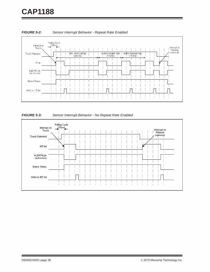
5.6.1 SENSOR INTERRUPT BEHAVIORThe sensor interrupts are generated in one of two ways:
1. An interrupt is generated when a touch is detected and, as a user selectable option, when a release is detected(by default - see Section 6.6). See Figure 5-3.
2. If the repeat rate is enabled then, so long as the touch is held, another interrupt will be generated based on theprogrammed repeat rate (see Figure 5-2).
When the repeat rate is enabled, the device uses an additional control called MPRESS that determines whether a touchis flagged as a simple “touch” or a “press and hold”. The MPRESS[3:0] bits set a minimum press timer. When the buttonis touched, the timer begins. If the sensor pad is released before the minimum press timer expires, it is flagged as atouch and an interrupt is generated upon release. If the sensor input detects a touch for longer than this timer value, itis flagged as a “press and hold” event. So long as the touch is held, interrupts will be generated at the programmedrepeat rate and upon release (if enabled).
APPLICATION NOTE: Figure 5-2 and Figure 5-3 show default operation which is to generate an interrupt uponsensor pad release and an active-low ALERT# pin.
APPLICATION NOTE: The host may need to poll the device twice to determine that a release has been detected.
Note: Delayed recalibration only works when the delta count is above the active sensor input threshold. Ifenabled, it is invoked when a sensor pad touch is held longer than the MAX_DUR bit setting.
CAP1188
DS00001620C-page 28 2015 Microchip Technology Inc.
FIGURE 5-2: Sensor Interrupt Behavior - Repeat Rate Enabled
FIGURE 5-3: Sensor Interrupt Behavior - No Repeat Rate Enabled
2015 Microchip Technology Inc. DS00001620C-page 29
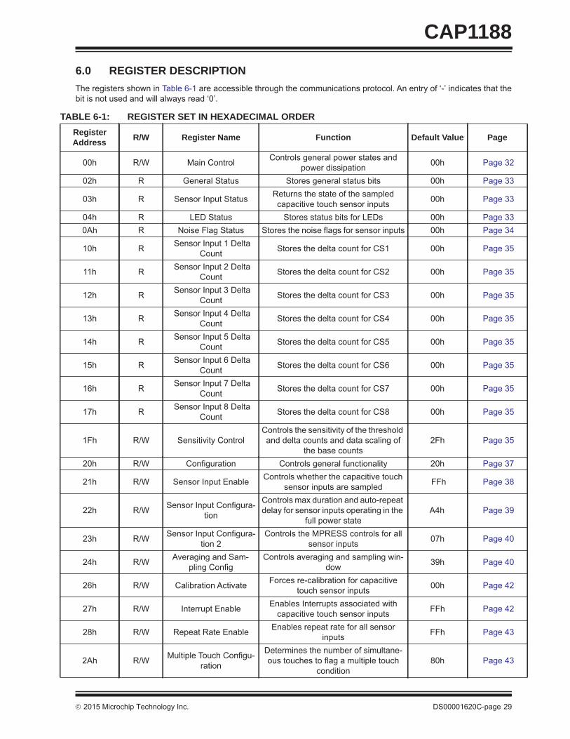
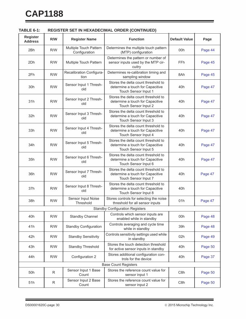
CAP11886.0 REGISTER DESCRIPTIONThe registers shown in Table 6-1 are accessible through the communications protocol. An entry of ‘-’ indicates that thebit is not used and will always read ‘0’.
TABLE 6-1: REGISTER SET IN HEXADECIMAL ORDER RegisterAddress R/W Register Name Function Default Value Page
00h R/W Main Control Controls general power states and power dissipation 00h Page 32
02h R General Status Stores general status bits 00h Page 33
03h R Sensor Input Status Returns the state of the sampled capacitive touch sensor inputs 00h Page 33
04h R LED Status Stores status bits for LEDs 00h Page 330Ah R Noise Flag Status Stores the noise flags for sensor inputs 00h Page 34
10h R Sensor Input 1 Delta Count Stores the delta count for CS1 00h Page 35
11h R Sensor Input 2 Delta Count Stores the delta count for CS2 00h Page 35
12h R Sensor Input 3 Delta Count Stores the delta count for CS3 00h Page 35
13h R Sensor Input 4 Delta Count Stores the delta count for CS4 00h Page 35
14h R Sensor Input 5 Delta Count Stores the delta count for CS5 00h Page 35
15h R Sensor Input 6 Delta Count Stores the delta count for CS6 00h Page 35
16h R Sensor Input 7 Delta Count Stores the delta count for CS7 00h Page 35
17h R Sensor Input 8 Delta Count Stores the delta count for CS8 00h Page 35
1Fh R/W Sensitivity ControlControls the sensitivity of the threshold and delta counts and data scaling of
the base counts2Fh Page 35
20h R/W Configuration Controls general functionality 20h Page 37
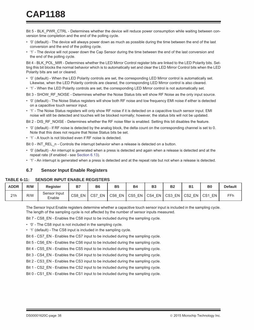
21h R/W Sensor Input Enable Controls whether the capacitive touch sensor inputs are sampled FFh Page 38
22h R/W Sensor Input Configura-tion
Controls max duration and auto-repeat delay for sensor inputs operating in the
full power stateA4h Page 39
23h R/W Sensor Input Configura-tion 2
Controls the MPRESS controls for all sensor inputs 07h Page 40
24h R/W Averaging and Sam-pling Config
Controls averaging and sampling win-dow 39h Page 40
26h R/W Calibration Activate Forces re-calibration for capacitive touch sensor inputs 00h Page 42
27h R/W Interrupt Enable Enables Interrupts associated with capacitive touch sensor inputs FFh Page 42
28h R/W Repeat Rate Enable Enables repeat rate for all sensor inputs FFh Page 43
2Ah R/W Multiple Touch Configu-ration
Determines the number of simultane-ous touches to flag a multiple touch
condition80h Page 43
CAP1188
DS00001620C-page 30 2015 Microchip Technology Inc.
2Bh R/W Multiple Touch Pattern Configuration
Determines the multiple touch pattern (MTP) configuration 00h Page 44
2Dh R/W Multiple Touch PatternDetermines the pattern or number of sensor inputs used by the MTP cir-
cuitryFFh Page 45
2Fh R/W Recalibration Configura-tion
Determines re-calibration timing and sampling window 8Ah Page 45
30h R/W Sensor Input 1 Thresh-old
Stores the delta count threshold to determine a touch for Capacitive
Touch Sensor Input 140h Page 47
31h R/W Sensor Input 2 Thresh-old
Stores the delta count threshold to determine a touch for Capacitive
Touch Sensor Input 240h Page 47
32h R/W Sensor Input 3 Thresh-old
Stores the delta count threshold to determine a touch for Capacitive
Touch Sensor Input 340h Page 47
33h R/W Sensor Input 4 Thresh-old
Stores the delta count threshold to determine a touch for Capacitive
Touch Sensor Input 440h Page 47
34h R/W Sensor Input 5 Thresh-old
Stores the delta count threshold to determine a touch for Capacitive
Touch Sensor Input 540h Page 47
35h R/W Sensor Input 6 Thresh-old
Stores the delta count threshold to determine a touch for Capacitive
Touch Sensor Input 640h Page 47
36h R/W Sensor Input 7 Thresh-old
Stores the delta count threshold to determine a touch for Capacitive
Touch Sensor Input 740h Page 47
37h R/W Sensor Input 8 Thresh-old
Stores the delta count threshold to determine a touch for Capacitive
Touch Sensor Input 840h
38h R/W Sensor Input Noise Threshold
Stores controls for selecting the noise threshold for all sensor inputs 01h Page 47
Standby Configuration Registers
40h R/W Standby Channel Controls which sensor inputs are enabled while in standby 00h Page 48
41h R/W Standby Configuration Controls averaging and cycle time while in standby 39h Page 48
42h R/W Standby Sensitivity Controls sensitivity settings used while in standby 02h Page 49
43h R/W Standby Threshold Stores the touch detection threshold for active sensor inputs in standby 40h Page 50
44h R/W Configuration 2 Stores additional configuration con-trols for the device 40h Page 37
Base Count Registers
50h R Sensor Input 1 Base Count
Stores the reference count value for sensor input 1 C8h Page 50
51h R Sensor Input 2 Base Count
Stores the reference count value for sensor input 2 C8h Page 50
TABLE 6-1: REGISTER SET IN HEXADECIMAL ORDER (CONTINUED) RegisterAddress R/W Register Name Function Default Value Page
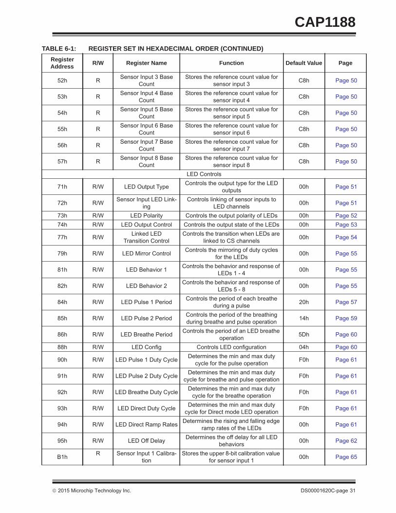
2015 Microchip Technology Inc. DS00001620C-page 31
CAP1188
52h R Sensor Input 3 Base Count
Stores the reference count value for sensor input 3 C8h Page 50
53h R Sensor Input 4 Base Count
Stores the reference count value for sensor input 4 C8h Page 50
54h R Sensor Input 5 Base Count
Stores the reference count value for sensor input 5 C8h Page 50
55h R Sensor Input 6 Base Count
Stores the reference count value for sensor input 6 C8h Page 50
56h R Sensor Input 7 Base Count
Stores the reference count value for sensor input 7 C8h Page 50
57h R Sensor Input 8 Base Count
Stores the reference count value for sensor input 8 C8h Page 50
LED Controls
71h R/W LED Output Type Controls the output type for the LED outputs 00h Page 51
72h R/W Sensor Input LED Link-ing
Controls linking of sensor inputs to LED channels 00h Page 51
73h R/W LED Polarity Controls the output polarity of LEDs 00h Page 5274h R/W LED Output Control Controls the output state of the LEDs 00h Page 53
77h R/W Linked LED Transition Control
Controls the transition when LEDs are linked to CS channels 00h Page 54
79h R/W LED Mirror Control Controls the mirroring of duty cycles for the LEDs 00h Page 55
81h R/W LED Behavior 1 Controls the behavior and response of LEDs 1 - 4 00h Page 55
82h R/W LED Behavior 2 Controls the behavior and response of LEDs 5 - 8 00h Page 55
84h R/W LED Pulse 1 Period Controls the period of each breathe during a pulse 20h Page 57
85h R/W LED Pulse 2 Period Controls the period of the breathing during breathe and pulse operation 14h Page 59
86h R/W LED Breathe Period Controls the period of an LED breathe operation 5Dh Page 60
88h R/W LED Config Controls LED configuration 04h Page 60
90h R/W LED Pulse 1 Duty Cycle Determines the min and max duty cycle for the pulse operation F0h Page 61
91h R/W LED Pulse 2 Duty Cycle Determines the min and max duty cycle for breathe and pulse operation F0h Page 61
92h R/W LED Breathe Duty Cycle Determines the min and max duty cycle for the breathe operation F0h Page 61
93h R/W LED Direct Duty Cycle Determines the min and max duty cycle for Direct mode LED operation F0h Page 61
94h R/W LED Direct Ramp Rates Determines the rising and falling edge ramp rates of the LEDs 00h Page 61
95h R/W LED Off Delay Determines the off delay for all LED behaviors 00h Page 62
B1h R Sensor Input 1 Calibra-tion
Stores the upper 8-bit calibration value for sensor input 1 00h Page 65
TABLE 6-1: REGISTER SET IN HEXADECIMAL ORDER (CONTINUED) RegisterAddress R/W Register Name Function Default Value Page
CAP1188
DS00001620C-page 32 2015 Microchip Technology Inc.
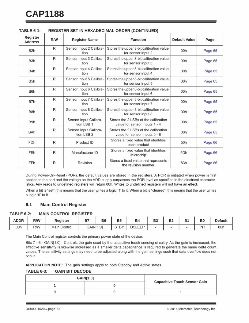
During Power-On-Reset (POR), the default values are stored in the registers. A POR is initiated when power is firstapplied to the part and the voltage on the VDD supply surpasses the POR level as specified in the electrical character-istics. Any reads to undefined registers will return 00h. Writes to undefined registers will not have an effect.
When a bit is “set”, this means that the user writes a logic ‘1’ to it. When a bit is “cleared”, this means that the user writesa logic ‘0’ to it.
6.1 Main Control Register
The Main Control register controls the primary power state of the device.
Bits 7 - 6 - GAIN[1:0] - Controls the gain used by the capacitive touch sensing circuitry. As the gain is increased, theeffective sensitivity is likewise increased as a smaller delta capacitance is required to generate the same delta countvalues. The sensitivity settings may need to be adjusted along with the gain settings such that data overflow does notoccur.
APPLICATION NOTE: The gain settings apply to both Standby and Active states.
B2h R Sensor Input 2 Calibra-tion
Stores the upper 8-bit calibration value for sensor input 2 00h Page 65
B3h R Sensor Input 3 Calibra-tion
Stores the upper 8-bit calibration value for sensor input 3 00h Page 65
B4h R Sensor Input 4 Calibra-tion
Stores the upper 8-bit calibration value for sensor input 4 00h Page 65
B5h R Sensor Input 5 Calibra-tion
Stores the upper 8-bit calibration value for sensor input 5 00h Page 65
B6h R Sensor Input 6 Calibra-tion
Stores the upper 8-bit calibration value for sensor input 6 00h Page 65
B7h R Sensor Input 7 Calibra-tion
Stores the upper 8-bit calibration value for sensor input 7 00h Page 65
B8h R Sensor Input 8 Calibra-tion
Stores the upper 8-bit calibration value for sensor input 8 00h Page 65
B9h R Sensor Input Calibra-tion LSB 1
Stores the 2 LSBs of the calibration value for sensor inputs 1 - 4 00h Page 65
BAh R Sensor Input Calibra-tion LSB 2
Stores the 2 LSBs of the calibration value for sensor inputs 5 - 8 00h Page 65
FDh R Product ID Stores a fixed value that identifies each product 50h Page 66
FEh R Manufacturer ID Stores a fixed value that identifies Microchip 5Dh Page 66
FFh R Revision Stores a fixed value that represents the revision number 83h Page 66
TABLE 6-2: MAIN CONTROL REGISTERADDR R/W Register B7 B6 B5 B4 B3 B2 B1 B0 Default
00h R/W Main Control GAIN[1:0] STBY DSLEEP - - - INT 00h
TABLE 6-3: GAIN BIT DECODE GAIN[1:0]
Capacitive Touch Sensor Gain1 0
0 0 1
TABLE 6-1: REGISTER SET IN HEXADECIMAL ORDER (CONTINUED) RegisterAddress R/W Register Name Function Default Value Page
2015 Microchip Technology Inc. DS00001620C-page 33
CAP1188
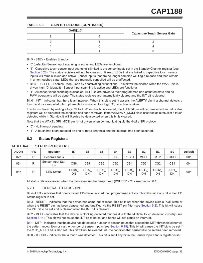
Bit 5 - STBY - Enables Standby.
• ‘0’ (default) - Sensor input scanning is active and LEDs are functional. • ‘1’ - Capacitive touch sensor input scanning is limited to the sensor inputs set in the Standby Channel register (see
Section 6.20). The status registers will not be cleared until read. LEDs that are linked to capacitive touch sensor inputs will remain linked and active. Sensor inputs that are no longer sampled will flag a release and then remain in a non-touched state. LEDs that are manually controlled will be unaffected.
• Bit 4 - DSLEEP - Enables Deep Sleep by deactivating all functions. This bit will be cleared when the WAKE pin is driven high. ‘0’ (default) - Sensor input scanning is active and LEDs are functional.
• ‘1’ - All sensor input scanning is disabled. All LEDs are driven to their programmed non-actuated state and no PWM operations will be done. The status registers are automatically cleared and the INT bit is cleared.
Bit 0 - INT - Indicates that there is an interrupt. When this bit is set, it asserts the ALERT# pin. If a channel detects atouch and its associated interrupt enable bit is not set to a logic ‘1’, no action is taken.
This bit is cleared by writing a logic ‘0’ to it. When this bit is cleared, the ALERT# pin will be deasserted and all statusregisters will be cleared if the condition has been removed. If the WAKE/SPI_MOSI pin is asserted as a result of a touchdetected while in Standby, it will likewise be deasserted when this bit is cleared.
Note that the WAKE / SPI_MOSI pin is not driven when communicating via the 4-wire SPI protocol.
• ‘0’ - No interrupt pending.• ‘1’ - A touch has been detected on one or more channels and the interrupt has been asserted.
6.2 Status Registers
All status bits are cleared when the device enters the Deep Sleep (DSLEEP = ‘1’ - see Section 6.1).
6.2.1 GENERAL STATUS - 02H Bit 4 - LED - Indicates that one or more LEDs have finished their programmed activity. This bit is set if any bit in the LEDStatus register is set.
Bit 3 - RESET - Indicates that the device has come out of reset. This bit is set when the device exits a POR state orwhen the RESET pin has been deasserted and qualified via the RESET pin filter (see Section 5.2). This bit will causethe INT bit to be set and is cleared when the INT bit is cleared.
Bit 2 - MULT - Indicates that the device is blocking detected touches due to the Multiple Touch detection circuitry (seeSection 6.14). This bit will not cause the INT bit to be set and hence will not cause an interrupt.
Bit 1 - MTP - Indicates that the device has detected a number of sensor inputs that exceed the MTP threshold either viathe pattern recognition or via the number of sensor inputs (see Section 6.15). This bit will cause the INT bit to be set ifthe MTP_ALERT bit is also set. This bit will not be cleared until the condition that caused it to be set has been removed.
Bit 0 - TOUCH - Indicates that a touch was detected. This bit is set if any bit in the Sensor Input Status register is set.
0 1 21 0 41 1 8
TABLE 6-4: STATUS REGISTERSADDR R/W Register B7 B6 B5 B4 B3 B2 B1 B0 Default
02h R General Status - - - LED RESET MULT MTP TOUCH 00h
03h R Sensor Input Sta-tus CS8 CS7 CS6 CS5 CS4 CS3 CS2 CS1 00h
04h R LED Status LED8_DN
LED7_DN
LED6_DN
LED5_DN
LED4_DN
LED3_DN
LED2_DN
LED1_DN 00h
TABLE 6-3: GAIN BIT DECODE (CONTINUED) GAIN[1:0]
Capacitive Touch Sensor Gain1 0
CAP1188
DS00001620C-page 34 2015 Microchip Technology Inc.
6.2.2 SENSOR INPUT STATUS - 03HThe Sensor Input Status Register stores status bits that indicate a touch has been detected. A value of ‘0’ in any bitindicates that no touch has been detected. A value of ‘1’ in any bit indicates that a touch has been detected.
All bits are cleared when the INT bit is cleared and if a touch on the respective capacitive touch sensor input is no longerpresent. If a touch is still detected, the bits will not be cleared (but this will not cause the interrupt to be asserted - seeSection 6.6).
Bit 7 - CS8 - Indicates that a touch was detected on Sensor Input 8. This sensor input can be linked to LED8.
Bit 6 - CS7 - Indicates that a touch was detected on Sensor Input 7. This sensor input can be linked to LED7.
Bit 5 - CS6 - Indicates that a touch was detected on Sensor Input 6. This sensor input can be linked to LED6.
Bit 4 - CS5 - Indicates that a touch was detected on Sensor Input 5. This sensor input can be linked to LED5.
Bit 3 - CS4 - Indicates that a touch was detected on Sensor Input 4. This sensor input can be linked to LED4.
Bit 2 - CS3 - Indicates that a touch was detected on Sensor Input 3. This sensor input can be linked to LED3.
Bit 1 - CS2 - Indicates that a touch was detected on Sensor Input 2. This sensor input can be linked to LED2.
Bit 0 - CS1 - Indicates that a touch was detected on Sensor Input 1. This sensor input can be linked to LED1.
6.2.3 LED STATUS - 04HThe LED Status Registers indicate when an LED has completed its configured behavior (see Section 6.31, "LED Behav-ior Registers") after being actuated by the host (see Section 6.28, "LED Output Control Register"). These bits areignored when the LED is linked to a capacitive sensor input. All LED Status bits are cleared when the INT bit is cleared.
Bit 7 - LED8_DN - Indicates that LED8 has finished its behavior after being actuated by the host.
Bit 6 - LED7_DN - Indicates that LED7 has finished its behavior after being actuated by the host.
Bit 5 - LED6_DN - Indicates that LED6 has finished its behavior after being actuated by the host.
Bit 4 - LED5_DN - Indicates that LED5 has finished its behavior after being actuated by the host.
Bit 3 - LED4_DN - Indicates that LED4 has finished its behavior after being actuated by the host.
Bit 2 - LED3_DN - Indicates that LED3 has finished its behavior after being actuated by the host.
Bit 1 - LED2_DN - Indicates that LED2 has finished its behavior after being actuated by the host.
Bit 0 - LED1_DN - Indicates that LED1 has finished its behavior after being actuated by the host.
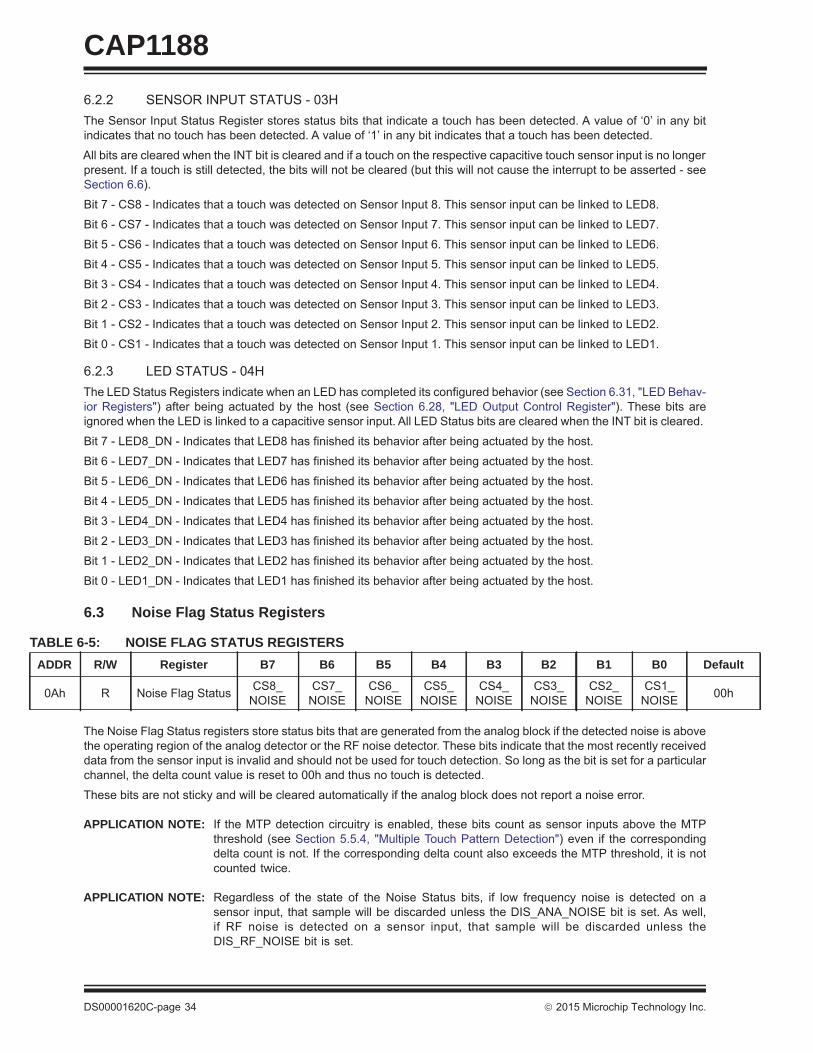
6.3 Noise Flag Status Registers
The Noise Flag Status registers store status bits that are generated from the analog block if the detected noise is abovethe operating region of the analog detector or the RF noise detector. These bits indicate that the most recently receiveddata from the sensor input is invalid and should not be used for touch detection. So long as the bit is set for a particularchannel, the delta count value is reset to 00h and thus no touch is detected.
These bits are not sticky and will be cleared automatically if the analog block does not report a noise error.
APPLICATION NOTE: If the MTP detection circuitry is enabled, these bits count as sensor inputs above the MTPthreshold (see Section 5.5.4, "Multiple Touch Pattern Detection") even if the correspondingdelta count is not. If the corresponding delta count also exceeds the MTP threshold, it is notcounted twice.
APPLICATION NOTE: Regardless of the state of the Noise Status bits, if low frequency noise is detected on asensor input, that sample will be discarded unless the DIS_ANA_NOISE bit is set. As well,if RF noise is detected on a sensor input, that sample will be discarded unless theDIS_RF_NOISE bit is set.
TABLE 6-5: NOISE FLAG STATUS REGISTERSADDR R/W Register B7 B6 B5 B4 B3 B2 B1 B0 Default
0Ah R Noise Flag Status CS8_NOISE
CS7_NOISE
CS6_NOISE
CS5_NOISE
CS4_NOISE
CS3_NOISE
CS2_NOISE
CS1_NOISE 00h
2015 Microchip Technology Inc. DS00001620C-page 35
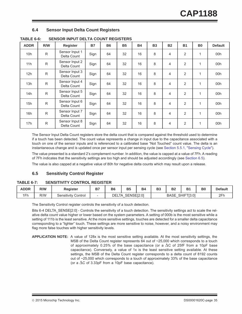
CAP11886.4 Sensor Input Delta Count Registers
The Sensor Input Delta Count registers store the delta count that is compared against the threshold used to determineif a touch has been detected. The count value represents a change in input due to the capacitance associated with atouch on one of the sensor inputs and is referenced to a calibrated base “Not Touched” count value. The delta is aninstantaneous change and is updated once per sensor input per sensing cycle (see Section 5.5.1, "Sensing Cycle").
The value presented is a standard 2’s complement number. In addition, the value is capped at a value of 7Fh. A readingof 7Fh indicates that the sensitivity settings are too high and should be adjusted accordingly (see Section 6.5).
The value is also capped at a negative value of 80h for negative delta counts which may result upon a release.
6.5 Sensitivity Control Register
The Sensitivity Control register controls the sensitivity of a touch detection.
Bits 6-4 DELTA_SENSE[2:0] - Controls the sensitivity of a touch detection. The sensitivity settings act to scale the rel-ative delta count value higher or lower based on the system parameters. A setting of 000b is the most sensitive while asetting of 111b is the least sensitive. At the more sensitive settings, touches are detected for a smaller delta capacitancecorresponding to a “lighter” touch. These settings are more sensitive to noise, however, and a noisy environment mayflag more false touches with higher sensitivity levels.
APPLICATION NOTE: A value of 128x is the most sensitive setting available. At the most sensitivity settings, theMSB of the Delta Count register represents 64 out of ~25,000 which corresponds to a touchof approximately 0.25% of the base capacitance (or a C of 25fF from a 10pF basecapacitance). Conversely, a value of 1x is the least sensitive setting available. At thesesettings, the MSB of the Delta Count register corresponds to a delta count of 8192 countsout of ~25,000 which corresponds to a touch of approximately 33% of the base capacitance(or a C of 3.33pF from a 10pF base capacitance).
TABLE 6-6: SENSOR INPUT DELTA COUNT REGISTERS ADDR R/W Register B7 B6 B5 B4 B3 B2 B1 B0 Default
10h R Sensor Input 1 Delta Count Sign 64 32 16 8 4 2 1 00h
11h R Sensor Input 2 Delta Count Sign 64 32 16 8 4 2 1 00h
12h R Sensor Input 3 Delta Count Sign 64 32 16 8 4 2 1 00h
13h R Sensor Input 4 Delta Count Sign 64 32 16 8 4 2 1 00h
14h R Sensor Input 5 Delta Count Sign 64 32 16 8 4 2 1 00h
15h R Sensor Input 6 Delta Count Sign 64 32 16 8 4 2 1 00h
16h R Sensor Input 7 Delta Count Sign 64 32 16 8 4 2 1 00h
17h R Sensor Input 8 Delta Count Sign 64 32 16 8 4 2 1 00h
TABLE 6-7: SENSITIVITY CONTROL REGISTERADDR R/W Register B7 B6 B5 B4 B3 B2 B1 B0 Default
1Fh R/W Sensitivity Control - DELTA_SENSE[2:0] BASE_SHIFT[3:0] 2Fh
CAP1188
DS00001620C-page 36 2015 Microchip Technology Inc.
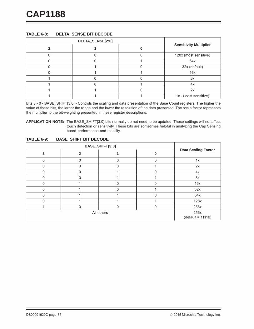
Bits 3 - 0 - BASE_SHIFT[3:0] - Controls the scaling and data presentation of the Base Count registers. The higher thevalue of these bits, the larger the range and the lower the resolution of the data presented. The scale factor representsthe multiplier to the bit-weighting presented in these register descriptions.
APPLICATION NOTE: The BASE_SHIFT[3:0] bits normally do not need to be updated. These settings will not affecttouch detection or sensitivity. These bits are sometimes helpful in analyzing the Cap Sensingboard performance and stability.
TABLE 6-8: DELTA_SENSE BIT DECODE DELTA_SENSE[2:0]
Sensitivity Multiplier2 1 0
0 0 0 128x (most sensitive)0 0 1 64x 0 1 0 32x (default) 0 1 1 16x1 0 0 8x1 0 1 4x1 1 0 2x1 1 1 1x - (least sensitive)
TABLE 6-9: BASE_SHIFT BIT DECODE BASE_SHIFT[3:0]
Data Scaling Factor3 2 1 0
0 0 0 0 1x0 0 0 1 2x0 0 1 0 4x0 0 1 1 8x0 1 0 0 16x0 1 0 1 32x0 1 1 0 64x0 1 1 1 128x1 0 0 0 256x
All others 256x (default = 1111b)
2015 Microchip Technology Inc. DS00001620C-page 37
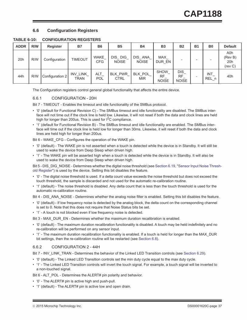
CAP11886.6 Configuration Registers
The Configuration registers control general global functionality that affects the entire device.
6.6.1 CONFIGURATION - 20HBit 7 - TIMEOUT - Enables the timeout and idle functionality of the SMBus protocol.
• ‘0’ (default for Functional Revision C) - The SMBus timeout and idle functionality are disabled. The SMBus inter-face will not time out if the clock line is held low. Likewise, it will not reset if both the data and clock lines are held high for longer than 200us. This is used for I2C compliance.
• ‘1’ (default for Functional Revision B) - The SMBus timeout and idle functionality are enabled. The SMBus inter-face will time out if the clock line is held low for longer than 30ms. Likewise, it will reset if both the data and clock lines are held high for longer than 200us.
Bit 6 - WAKE_CFG - Configures the operation of the WAKE pin.
• ‘0’ (default) - The WAKE pin is not asserted when a touch is detected while the device is in Standby. It will still be used to wake the device from Deep Sleep when driven high.
• ‘1’ - The WAKE pin will be asserted high when a touch is detected while the device is in Standby. It will also be used to wake the device from Deep Sleep when driven high.
Bit 5 - DIS_DIG_NOISE - Determines whether the digital noise threshold (see Section 6.19, "Sensor Input Noise Thresh-old Register") is used by the device. Setting this bit disables the feature.
• ‘0’ - The digital noise threshold is used. If a delta count value exceeds the noise threshold but does not exceed the touch threshold, the sample is discarded and not used for the automatic re-calibration routine.
• ‘1’ (default) - The noise threshold is disabled. Any delta count that is less than the touch threshold is used for the automatic re-calibration routine.
Bit 4 - DIS_ANA_NOISE - Determines whether the analog noise filter is enabled. Setting this bit disables the feature.
• ‘0’ (default) - If low frequency noise is detected by the analog block, the delta count on the corresponding channel is set to 0. Note that this does not require that Noise Status bits be set.
• ‘1’ - A touch is not blocked even if low frequency noise is detected.
Bit 3 - MAX_DUR_EN - Determines whether the maximum duration recalibration is enabled.
• ‘0’ (default) - The maximum duration recalibration functionality is disabled. A touch may be held indefinitely and no re-calibration will be performed on any sensor input.
• ‘1’ - The maximum duration recalibration functionality is enabled. If a touch is held for longer than the MAX_DUR bit settings, then the re-calibration routine will be restarted (see Section 6.8).
6.6.2 CONFIGURATION 2 - 44HBit 7 - INV_LINK_TRAN - Determines the behavior of the Linked LED Transition controls (see Section 6.29).
• ‘0’ (default) - The Linked LED Transition controls set the min duty cycle equal to the max duty cycle.• ‘1’ - The Linked LED Transition controls will invert the touch signal. For example, a touch signal will be inverted to
a non-touched signal.
Bit 6 - ALT_POL - Determines the ALERT# pin polarity and behavior.
• ‘0’ - The ALERT# pin is active high and push-pull. • ‘1’ (default) - The ALERT# pin is active low and open drain.
TABLE 6-10: CONFIGURATION REGISTERS ADDR R/W Register B7 B6 B5 B4 B3 B2 B1 B0 Default
20h R/W Configuration TIMEOUT WAKE_CFG
DIS_ DIG_NOISE
DIS_ ANA_NOISE
MAX_ DUR_EN - - -
A0h(Rev B)
20h(rev C)
44h R/W Configuration 2 INV_LINK_TRAN
ALT_POL
BLK_PWR_CTRL
BLK_POL_MIR
SHOW_RF_
NOISE
DIS_RF_
NOISE- INT_
REL_n 40h
CAP1188
DS00001620C-page 38 2015 Microchip Technology Inc.
Bit 5 - BLK_PWR_CTRL - Determines whether the device will reduce power consumption while waiting between con-version time completion and the end of the polling cycle.
• ‘0’ (default) - The device will always power down as much as possible during the time between the end of the last conversion and the end of the polling cycle.
• ‘1’ - The device will not power down the Cap Sensor during the time between the end of the last conversion and the end of the polling cycle.
Bit 4 - BLK_POL_MIR - Determines whether the LED Mirror Control register bits are linked to the LED Polarity bits. Set-ting this bit blocks the normal behavior which is to automatically set and clear the LED Mirror Control bits when the LEDPolarity bits are set or cleared.
• ‘0’ (default) - When the LED Polarity controls are set, the corresponding LED Mirror control is automatically set. Likewise, when the LED Polarity controls are cleared, the corresponding LED Mirror control is also cleared.
• ‘1’ - When the LED Polarity controls are set, the corresponding LED Mirror control is not automatically set.
Bit 3 - SHOW_RF_NOISE - Determines whether the Noise Status bits will show RF Noise as the only input source.
• ‘0’ (default) - The Noise Status registers will show both RF noise and low frequency EMI noise if either is detected on a capacitive touch sensor input.
• ‘1’ - The Noise Status registers will only show RF noise if it is detected on a capacitive touch sensor input. EMI noise will still be detected and touches will be blocked normally; however, the status bits will not be updated.
Bit 2 - DIS_RF_NOISE - Determines whether the RF noise filter is enabled. Setting this bit disables the feature.
• ‘0’ (default) - If RF noise is detected by the analog block, the delta count on the corresponding channel is set to 0. Note that this does not require that Noise Status bits be set.
• ‘1’ - A touch is not blocked even if RF noise is detected.
Bit 0 - INT_REL_n - Controls the interrupt behavior when a release is detected on a button.
• ‘0’ (default) - An interrupt is generated when a press is detected and again when a release is detected and at the repeat rate (if enabled - see Section 6.13).
• ‘1’ - An interrupt is generated when a press is detected and at the repeat rate but not when a release is detected.
6.7 Sensor Input Enable Registers
The Sensor Input Enable registers determine whether a capacitive touch sensor input is included in the sampling cycle.The length of the sampling cycle is not affected by the number of sensor inputs measured.
Bit 7 - CS8_EN - Enables the CS8 input to be included during the sampling cycle.
• ‘0’ - The CS8 input is not included in the sampling cycle.• ‘1’ (default) - The CS8 input is included in the sampling cycle.
Bit 6 - CS7_EN - Enables the CS7 input to be included during the sampling cycle.
Bit 5 - CS6_EN - Enables the CS6 input to be included during the sampling cycle.
Bit 4 - CS5_EN - Enables the CS5 input to be included during the sampling cycle.
Bit 3 - CS4_EN - Enables the CS4 input to be included during the sampling cycle.
Bit 2 - CS3_EN - Enables the CS3 input to be included during the sampling cycle.
Bit 1 - CS2_EN - Enables the CS2 input to be included during the sampling cycle.
Bit 0 - CS1_EN - Enables the CS1 input to be included during the sampling cycle.
TABLE 6-11: SENSOR INPUT ENABLE REGISTERSADDR R/W Register B7 B6 B5 B4 B3 B2 B1 B0 Default
21h R/W Sensor Input Enable CS8_EN CS7_EN CS6_EN CS5_EN CS4_EN CS3_EN CS2_EN CS1_EN FFh
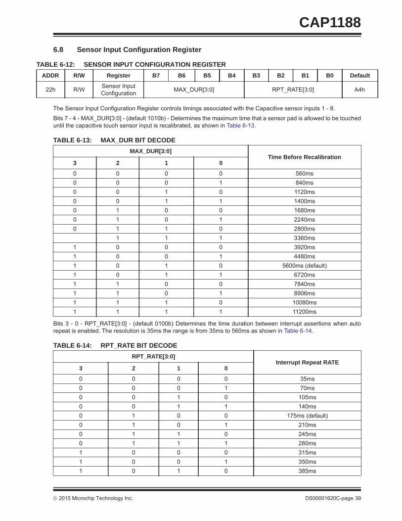
2015 Microchip Technology Inc. DS00001620C-page 39
CAP11886.8 Sensor Input Configuration Register
The Sensor Input Configuration Register controls timings associated with the Capacitive sensor inputs 1 - 8.
Bits 7 - 4 - MAX_DUR[3:0] - (default 1010b) - Determines the maximum time that a sensor pad is allowed to be toucheduntil the capacitive touch sensor input is recalibrated, as shown in Table 6-13.
Bits 3 - 0 - RPT_RATE[3:0] - (default 0100b) Determines the time duration between interrupt assertions when autorepeat is enabled. The resolution is 35ms the range is from 35ms to 560ms as shown in Table 6-14.
TABLE 6-12: SENSOR INPUT CONFIGURATION REGISTERADDR R/W Register B7 B6 B5 B4 B3 B2 B1 B0 Default
22h R/W Sensor Input Configuration MAX_DUR[3:0] RPT_RATE[3:0] A4h
TABLE 6-13: MAX_DUR BIT DECODE MAX_DUR[3:0]
Time Before Recalibration3 2 1 0
0 0 0 0 560ms0 0 0 1 840ms0 0 1 0 1120ms0 0 1 1 1400ms0 1 0 0 1680ms0 1 0 1 2240ms0 1 1 0 2800ms
1 1 1 3360ms1 0 0 0 3920ms1 0 0 1 4480ms1 0 1 0 5600ms (default) 1 0 1 1 6720ms1 1 0 0 7840ms1 1 0 1 8906ms1 1 1 0 10080ms1 1 1 1 11200ms
TABLE 6-14: RPT_RATE BIT DECODE RPT_RATE[3:0]
Interrupt Repeat RATE3 2 1 0
0 0 0 0 35ms0 0 0 1 70ms0 0 1 0 105ms0 0 1 1 140ms0 1 0 0 175ms (default) 0 1 0 1 210ms0 1 1 0 245ms0 1 1 1 280ms1 0 0 0 315ms1 0 0 1 350ms1 0 1 0 385ms
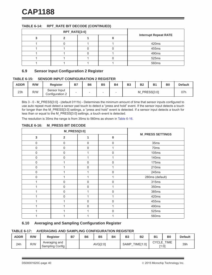
CAP1188
DS00001620C-page 40 2015 Microchip Technology Inc.
6.9 Sensor Input Configuration 2 Register
Bits 3 - 0 - M_PRESS[3:0] - (default 0111b) - Determines the minimum amount of time that sensor inputs configured touse auto repeat must detect a sensor pad touch to detect a “press and hold” event. If the sensor input detects a touchfor longer than the M_PRESS[3:0] settings, a “press and hold” event is detected. If a sensor input detects a touch forless than or equal to the M_PRESS[3:0] settings, a touch event is detected.
The resolution is 35ms the range is from 35ms to 560ms as shown in Table 6-16.
6.10 Averaging and Sampling Configuration Register
1 0 1 1 420ms1 1 0 0 455ms1 1 0 1 490ms1 1 1 0 525ms1 1 1 1 560ms
TABLE 6-15: SENSOR INPUT CONFIGURATION 2 REGISTERADDR R/W Register B7 B6 B5 B4 B3 B2 B1 B0 Default
23h R/W Sensor Input Configuration 2 - - - - M_PRESS[3:0] 07h
TABLE 6-16: M_PRESS BIT DECODE M_PRESS[3:0]
M_PRESS SETTINGS3 2 1 0
0 0 0 0 35ms0 0 0 1 70ms0 0 1 0 105ms0 0 1 1 140ms0 1 0 0 175ms0 1 0 1 210ms0 1 1 0 245ms0 1 1 1 280ms (default) 1 0 0 0 315ms1 0 0 1 350ms1 0 1 0 385ms1 0 1 1 420ms1 1 0 0 455ms1 1 0 1 490ms1 1 1 0 525ms1 1 1 1 560ms
TABLE 6-17: AVERAGING AND SAMPLING CONFIGURATION REGISTERADDR R/W Register B7 B6 B5 B4 B3 B2 B1 B0 Default
24h R/W Averaging and Sampling Config AVG[2:0] SAMP_TIME[1:0] CYCLE_TIME
[1:0] 39h
TABLE 6-14: RPT_RATE BIT DECODE (CONTINUED) RPT_RATE[3:0]
Interrupt Repeat RATE3 2 1 0
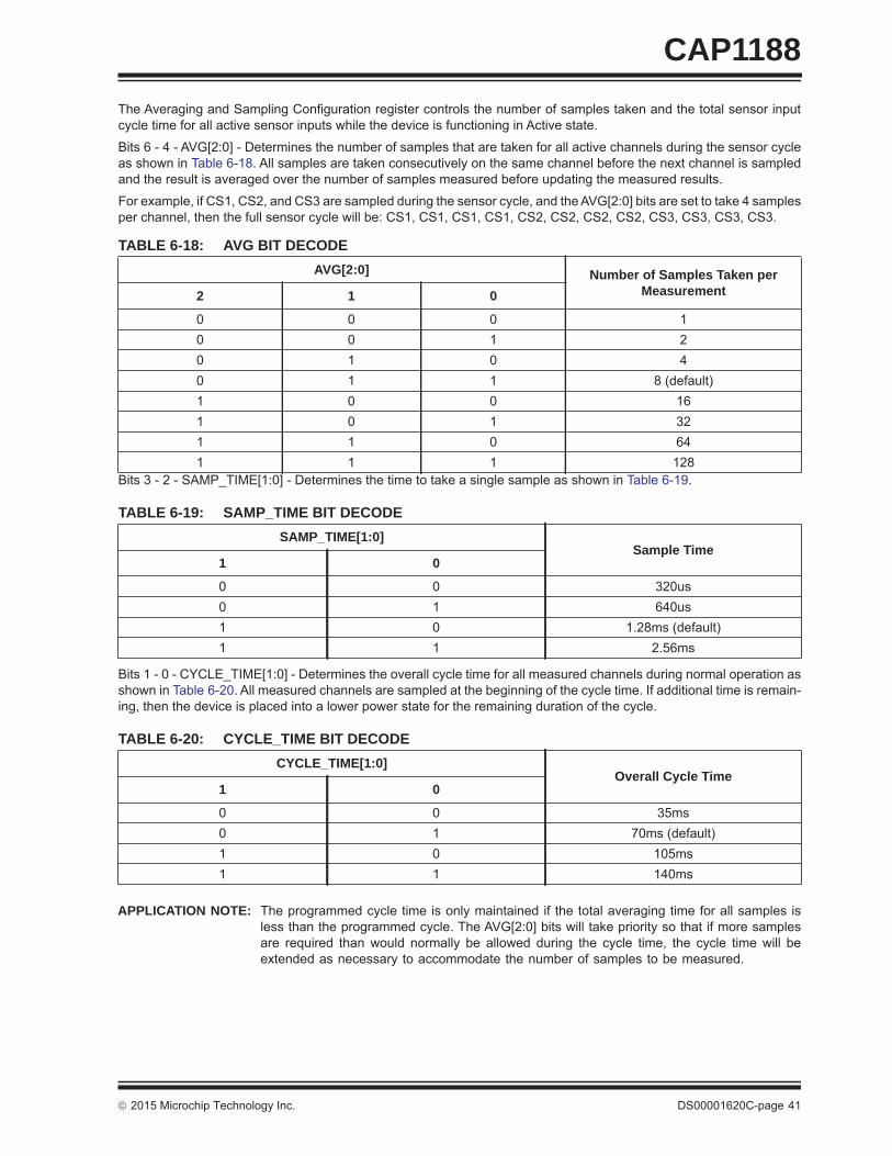
2015 Microchip Technology Inc. DS00001620C-page 41
CAP1188The Averaging and Sampling Configuration register controls the number of samples taken and the total sensor inputcycle time for all active sensor inputs while the device is functioning in Active state.
Bits 6 - 4 - AVG[2:0] - Determines the number of samples that are taken for all active channels during the sensor cycleas shown in Table 6-18. All samples are taken consecutively on the same channel before the next channel is sampledand the result is averaged over the number of samples measured before updating the measured results.
For example, if CS1, CS2, and CS3 are sampled during the sensor cycle, and the AVG[2:0] bits are set to take 4 samplesper channel, then the full sensor cycle will be: CS1, CS1, CS1, CS1, CS2, CS2, CS2, CS2, CS3, CS3, CS3, CS3.
Bits 3 - 2 - SAMP_TIME[1:0] - Determines the time to take a single sample as shown in Table 6-19.
Bits 1 - 0 - CYCLE_TIME[1:0] - Determines the overall cycle time for all measured channels during normal operation asshown in Table 6-20. All measured channels are sampled at the beginning of the cycle time. If additional time is remain-ing, then the device is placed into a lower power state for the remaining duration of the cycle.
APPLICATION NOTE: The programmed cycle time is only maintained if the total averaging time for all samples isless than the programmed cycle. The AVG[2:0] bits will take priority so that if more samplesare required than would normally be allowed during the cycle time, the cycle time will beextended as necessary to accommodate the number of samples to be measured.
TABLE 6-18: AVG BIT DECODE AVG[2:0] Number of Samples Taken per
Measurement2 1 0
0 0 0 1 0 0 1 20 1 0 40 1 1 8 (default) 1 0 0 161 0 1 321 1 0 641 1 1 128
TABLE 6-19: SAMP_TIME BIT DECODE SAMP_TIME[1:0]
Sample Time1 0
0 0 320us0 1 640us1 0 1.28ms (default) 1 1 2.56ms
TABLE 6-20: CYCLE_TIME BIT DECODE CYCLE_TIME[1:0]
Overall Cycle Time1 0
0 0 35ms 0 1 70ms (default) 1 0 105ms1 1 140ms
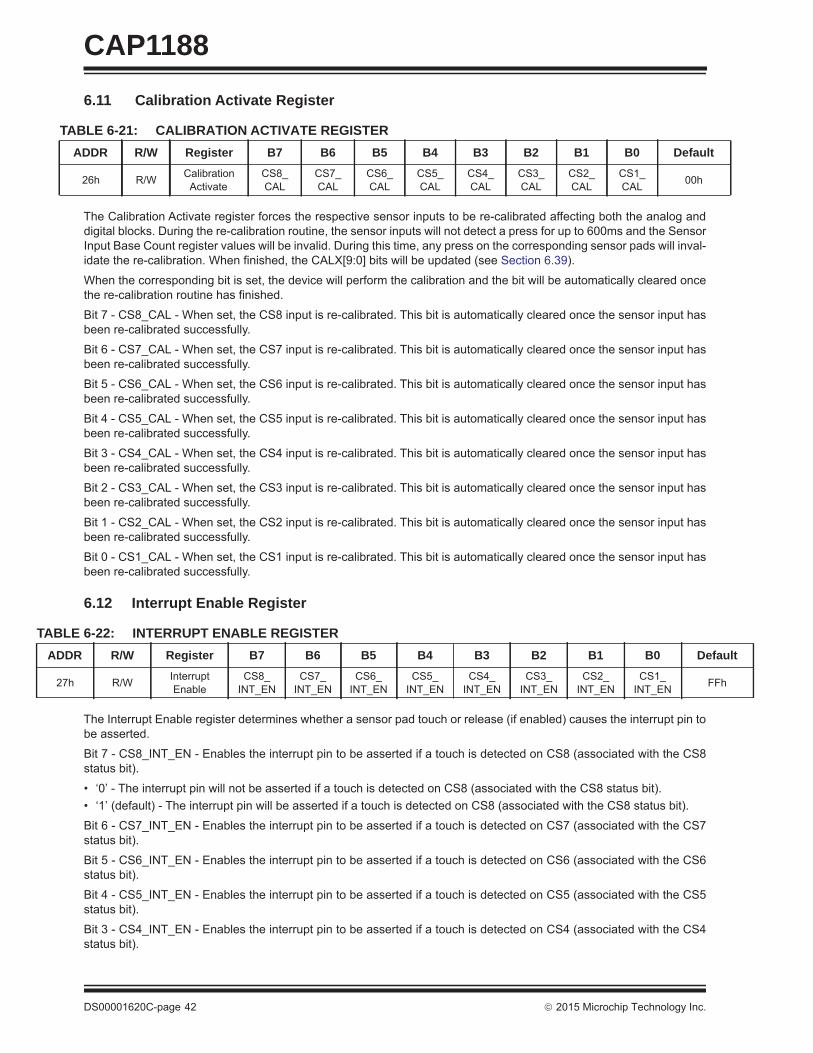
CAP1188
DS00001620C-page 42 2015 Microchip Technology Inc.
6.11 Calibration Activate Register
The Calibration Activate register forces the respective sensor inputs to be re-calibrated affecting both the analog anddigital blocks. During the re-calibration routine, the sensor inputs will not detect a press for up to 600ms and the SensorInput Base Count register values will be invalid. During this time, any press on the corresponding sensor pads will inval-idate the re-calibration. When finished, the CALX[9:0] bits will be updated (see Section 6.39).
When the corresponding bit is set, the device will perform the calibration and the bit will be automatically cleared oncethe re-calibration routine has finished.
Bit 7 - CS8_CAL - When set, the CS8 input is re-calibrated. This bit is automatically cleared once the sensor input hasbeen re-calibrated successfully.
Bit 6 - CS7_CAL - When set, the CS7 input is re-calibrated. This bit is automatically cleared once the sensor input hasbeen re-calibrated successfully.
Bit 5 - CS6_CAL - When set, the CS6 input is re-calibrated. This bit is automatically cleared once the sensor input hasbeen re-calibrated successfully.
Bit 4 - CS5_CAL - When set, the CS5 input is re-calibrated. This bit is automatically cleared once the sensor input hasbeen re-calibrated successfully.
Bit 3 - CS4_CAL - When set, the CS4 input is re-calibrated. This bit is automatically cleared once the sensor input hasbeen re-calibrated successfully.
Bit 2 - CS3_CAL - When set, the CS3 input is re-calibrated. This bit is automatically cleared once the sensor input hasbeen re-calibrated successfully.
Bit 1 - CS2_CAL - When set, the CS2 input is re-calibrated. This bit is automatically cleared once the sensor input hasbeen re-calibrated successfully.
Bit 0 - CS1_CAL - When set, the CS1 input is re-calibrated. This bit is automatically cleared once the sensor input hasbeen re-calibrated successfully.
6.12 Interrupt Enable Register
The Interrupt Enable register determines whether a sensor pad touch or release (if enabled) causes the interrupt pin tobe asserted.
Bit 7 - CS8_INT_EN - Enables the interrupt pin to be asserted if a touch is detected on CS8 (associated with the CS8status bit).
• ‘0’ - The interrupt pin will not be asserted if a touch is detected on CS8 (associated with the CS8 status bit).• ‘1’ (default) - The interrupt pin will be asserted if a touch is detected on CS8 (associated with the CS8 status bit).
Bit 6 - CS7_INT_EN - Enables the interrupt pin to be asserted if a touch is detected on CS7 (associated with the CS7status bit).
Bit 5 - CS6_INT_EN - Enables the interrupt pin to be asserted if a touch is detected on CS6 (associated with the CS6status bit).
Bit 4 - CS5_INT_EN - Enables the interrupt pin to be asserted if a touch is detected on CS5 (associated with the CS5status bit).
Bit 3 - CS4_INT_EN - Enables the interrupt pin to be asserted if a touch is detected on CS4 (associated with the CS4status bit).
TABLE 6-21: CALIBRATION ACTIVATE REGISTERADDR R/W Register B7 B6 B5 B4 B3 B2 B1 B0 Default
26h R/W Calibration Activate
CS8_ CAL
CS7_ CAL
CS6_ CAL
CS5_ CAL
CS4_ CAL
CS3_ CAL
CS2_ CAL
CS1_ CAL 00h
TABLE 6-22: INTERRUPT ENABLE REGISTERADDR R/W Register B7 B6 B5 B4 B3 B2 B1 B0 Default
27h R/W Interrupt Enable
CS8_INT_EN
CS7_INT_EN
CS6_INT_EN
CS5_INT_EN
CS4_INT_EN
CS3_INT_EN
CS2_INT_EN
CS1_INT_EN FFh
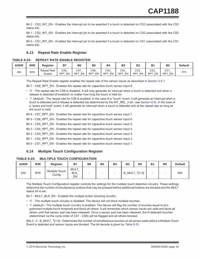
2015 Microchip Technology Inc. DS00001620C-page 43
CAP1188Bit 2 - CS3_INT_EN - Enables the interrupt pin to be asserted if a touch is detected on CS3 (associated with the CS3status bit).
Bit 1 - CS2_INT_EN - Enables the interrupt pin to be asserted if a touch is detected on CS2 (associated with the CS2status bit).
Bit 0 - CS1_INT_EN - Enables the interrupt pin to be asserted if a touch is detected on CS1 (associated with the CS1status bit).
6.13 Repeat Rate Enable Register
The Repeat Rate Enable register enables the repeat rate of the sensor inputs as described in Section 5.6.1.
Bit 7 - CS8_RPT_EN - Enables the repeat rate for capacitive touch sensor input 8.
• ‘0’ - The repeat rate for CS8 is disabled. It will only generate an interrupt when a touch is detected and when a release is detected (if enabled) no matter how long the touch is held for.
• ‘1’ (default) - The repeat rate for CS8 is enabled. In the case of a “touch” event, it will generate an interrupt when a touch is detected and a release is detected (as determined by the INT_REL_n bit - see Section 6.6). In the case of a “press and hold” event, it will generate an interrupt when a touch is detected and at the repeat rate so long as the touch is held.
Bit 6 - CS7_RPT_EN - Enables the repeat rate for capacitive touch sensor input 7.
Bit 5 - CS6_RPT_EN - Enables the repeat rate for capacitive touch sensor input 6.
Bit 4 - CS5_RPT_EN - Enables the repeat rate for capacitive touch sensor input 5.
Bit 3 - CS4_RPT_EN - Enables the repeat rate for capacitive touch sensor input 4.
Bit 2 - CS3_RPT_EN - Enables the repeat rate for capacitive touch sensor input 3.
Bit 1 - CS2_RPT_EN - Enables the repeat rate for capacitive touch sensor input 2.
Bit 0 - CS1_RPT_EN - Enables the repeat rate for capacitive touch sensor input 1.
6.14 Multiple Touch Configuration Register
The Multiple Touch Configuration register controls the settings for the multiple touch detection circuitry. These settingsdetermine the number of simultaneous buttons that may be pressed before additional buttons are blocked and the MULTstatus bit is set.
Bit 7 - MULT_BLK_EN - Enables the multiple button blocking circuitry.
• ‘0’ - The multiple touch circuitry is disabled. The device will not block multiple touches.• ‘1’ (default) - The multiple touch circuitry is enabled. The device will flag the number of touches equal to pro-
grammed multiple touch threshold and block all others. It will remember which sensor inputs are valid and block all others until that sensor pad has been released. Once a sensor pad has been released, the N detected touches (determined via the cycle order of CS1 - CS8) will be flagged and all others blocked.
Bits 3 - 2 - B_MULT_T[1:0] - Determines the number of simultaneous touches on all sensor pads before a Multiple TouchEvent is detected and sensor inputs are blocked. The bit decode is given by Table 6-25.
TABLE 6-23: REPEAT RATE ENABLE REGISTERADDR R/W Register B7 B6 B5 B4 B3 B2 B1 B0 Default
28h R/W Repeat Rate Enable
CS8_RPT_EN
CS7_RPT_EN
CS6_RPT_EN
CS5_RPT_EN
CS4_RPT_EN
CS3_RPT_EN
CS2_RPT_EN
CS1_RPT_EN FFh
TABLE 6-24: MULTIPLE TOUCH CONFIGURATIONADDR R/W Register B7 B6 B5 B4 B3 B2 B1 B0 Default
2Ah R/W Multiple Touch Config
MULT_BLK_ EN
- - - B_MULT_T[1:0] - - 80h
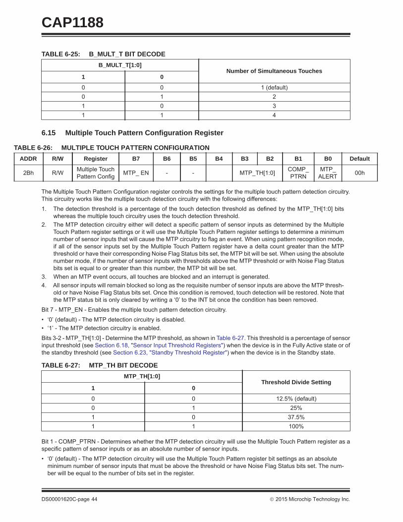
CAP1188
DS00001620C-page 44 2015 Microchip Technology Inc.
6.15 Multiple Touch Pattern Configuration Register
The Multiple Touch Pattern Configuration register controls the settings for the multiple touch pattern detection circuitry.This circuitry works like the multiple touch detection circuitry with the following differences:
1. The detection threshold is a percentage of the touch detection threshold as defined by the MTP_TH[1:0] bitswhereas the multiple touch circuitry uses the touch detection threshold.
2. The MTP detection circuitry either will detect a specific pattern of sensor inputs as determined by the MultipleTouch Pattern register settings or it will use the Multiple Touch Pattern register settings to determine a minimumnumber of sensor inputs that will cause the MTP circuitry to flag an event. When using pattern recognition mode,if all of the sensor inputs set by the Multiple Touch Pattern register have a delta count greater than the MTPthreshold or have their corresponding Noise Flag Status bits set, the MTP bit will be set. When using the absolutenumber mode, if the number of sensor inputs with thresholds above the MTP threshold or with Noise Flag Statusbits set is equal to or greater than this number, the MTP bit will be set.
3. When an MTP event occurs, all touches are blocked and an interrupt is generated.4. All sensor inputs will remain blocked so long as the requisite number of sensor inputs are above the MTP thresh-
old or have Noise Flag Status bits set. Once this condition is removed, touch detection will be restored. Note thatthe MTP status bit is only cleared by writing a ‘0’ to the INT bit once the condition has been removed.
Bit 7 - MTP_EN - Enables the multiple touch pattern detection circuitry.
• ‘0’ (default) - The MTP detection circuitry is disabled.• ‘1’ - The MTP detection circuitry is enabled.
Bits 3-2 - MTP_TH[1:0] - Determine the MTP threshold, as shown in Table 6-27. This threshold is a percentage of sensorinput threshold (see Section 6.18, "Sensor Input Threshold Registers") when the device is in the Fully Active state or ofthe standby threshold (see Section 6.23, "Standby Threshold Register") when the device is in the Standby state.
Bit 1 - COMP_PTRN - Determines whether the MTP detection circuitry will use the Multiple Touch Pattern register as aspecific pattern of sensor inputs or as an absolute number of sensor inputs.
• ‘0’ (default) - The MTP detection circuitry will use the Multiple Touch Pattern register bit settings as an absolute minimum number of sensor inputs that must be above the threshold or have Noise Flag Status bits set. The num-ber will be equal to the number of bits set in the register.
TABLE 6-25: B_MULT_T BIT DECODEB_MULT_T[1:0]
Number of Simultaneous Touches1 0
0 0 1 (default) 0 1 21 0 31 1 4
TABLE 6-26: MULTIPLE TOUCH PATTERN CONFIGURATIONADDR R/W Register B7 B6 B5 B4 B3 B2 B1 B0 Default
2Bh R/W Multiple Touch Pattern Config MTP_ EN - - MTP_TH[1:0] COMP_
PTRNMTP_
ALERT 00h
TABLE 6-27: MTP_TH BIT DECODE MTP_TH[1:0]
Threshold Divide Setting1 0
0 0 12.5% (default) 0 1 25% 1 0 37.5%1 1 100%
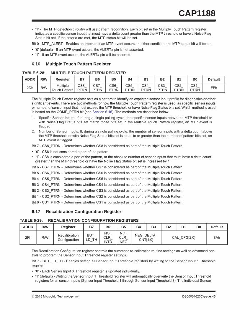
2015 Microchip Technology Inc. DS00001620C-page 45
CAP1188• ‘1’ - The MTP detection circuitry will use pattern recognition. Each bit set in the Multiple Touch Pattern register
indicates a specific sensor input that must have a delta count greater than the MTP threshold or have a Noise Flag Status bit set. If the criteria are met, the MTP status bit will be set.
Bit 0 - MTP_ALERT - Enables an interrupt if an MTP event occurs. In either condition, the MTP status bit will be set.
• ‘0’ (default) - If an MTP event occurs, the ALERT# pin is not asserted. • ‘1’ - If an MTP event occurs, the ALERT# pin will be asserted.
6.16 Multiple Touch Pattern Register
The Multiple Touch Pattern register acts as a pattern to identify an expected sensor input profile for diagnostics or othersignificant events. There are two methods for how the Multiple Touch Pattern register is used: as specific sensor inputsor number of sensor input that must exceed the MTP threshold or have Noise Flag Status bits set. Which method is usedis based on the COMP_PTRN bit (see Section 6.15). The methods are described below.
1. Specific Sensor Inputs: If, during a single polling cycle, the specific sensor inputs above the MTP threshold orwith Noise Flag Status bits set match those bits set in the Multiple Touch Pattern register, an MTP event isflagged.
2. Number of Sensor Inputs: If, during a single polling cycle, the number of sensor inputs with a delta count abovethe MTP threshold or with Noise Flag Status bits set is equal to or greater than the number of pattern bits set, anMTP event is flagged.
Bit 7 - CS8_PTRN - Determines whether CS8 is considered as part of the Multiple Touch Pattern.
• ‘0’ - CS8 is not considered a part of the pattern.• ‘1’ - CS8 is considered a part of the pattern, or the absolute number of sensor inputs that must have a delta count
greater than the MTP threshold or have the Noise Flag Status bit set is increased by 1.
Bit 6 - CS7_PTRN - Determines whether CS7 is considered as part of the Multiple Touch Pattern.
Bit 5 - CS6_PTRN - Determines whether CS6 is considered as part of the Multiple Touch Pattern.
Bit 4 - CS5_PTRN - Determines whether CS5 is considered as part of the Multiple Touch Pattern.
Bit 3 - CS4_PTRN - Determines whether CS4 is considered as part of the Multiple Touch Pattern.
Bit 2 - CS3_PTRN - Determines whether CS3 is considered as part of the Multiple Touch Pattern.
Bit 1 - CS2_PTRN - Determines whether CS2 is considered as part of the Multiple Touch Pattern.
Bit 0 - CS1_PTRN - Determines whether CS1 is considered as part of the Multiple Touch Pattern.
6.17 Recalibration Configuration Register
The Recalibration Configuration register controls the automatic re-calibration routine settings as well as advanced con-trols to program the Sensor Input Threshold register settings.
Bit 7 - BUT_LD_TH - Enables setting all Sensor Input Threshold registers by writing to the Sensor Input 1 Thresholdregister.
• ‘0’ - Each Sensor Input X Threshold register is updated individually. • ‘1’ (default) - Writing the Sensor Input 1 Threshold register will automatically overwrite the Sensor Input Threshold
registers for all sensor inputs (Sensor Input Threshold 1 through Sensor Input Threshold 8). The individual Sensor
TABLE 6-28: MULTIPLE TOUCH PATTERN REGISTERADDR R/W Register B7 B6 B5 B4 B3 B2 B1 B0 Default
2Dh R/W Multiple Touch Pattern
CS8_PTRN
CS7_PTRN
CS6_PTRN
CS5_PTRN
CS4_PTRN
CS3_PTRN
CS2_PTRN
CS1_PTRN FFh
TABLE 6-29: RECALIBRATION CONFIGURATION REGISTERSADDR R/W Register B7 B6 B5 B4 B3 B2 B1 B0 Default
2Fh R/W Recalibration Configuration
BUT_LD_TH
NO_CLR_INTD
NO_CLR_NEG
NEG_DELTA_CNT[1:0] CAL_CFG[2:0] 8Ah
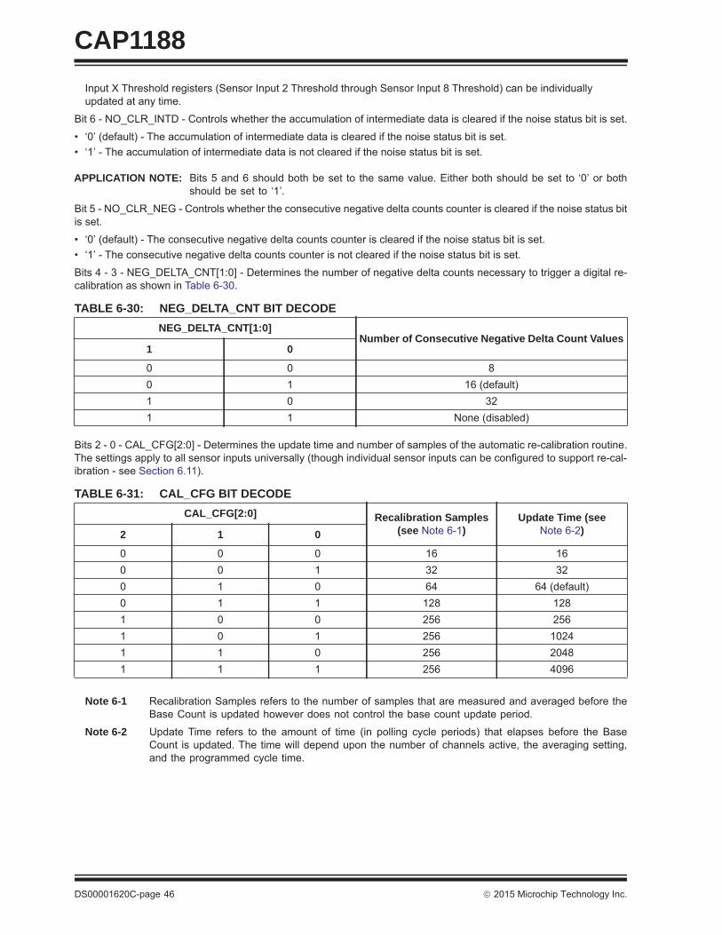
CAP1188
DS00001620C-page 46 2015 Microchip Technology Inc.
Input X Threshold registers (Sensor Input 2 Threshold through Sensor Input 8 Threshold) can be individually updated at any time.
Bit 6 - NO_CLR_INTD - Controls whether the accumulation of intermediate data is cleared if the noise status bit is set.
• ‘0’ (default) - The accumulation of intermediate data is cleared if the noise status bit is set.• ‘1’ - The accumulation of intermediate data is not cleared if the noise status bit is set.
APPLICATION NOTE: Bits 5 and 6 should both be set to the same value. Either both should be set to ‘0’ or bothshould be set to ‘1’.
Bit 5 - NO_CLR_NEG - Controls whether the consecutive negative delta counts counter is cleared if the noise status bitis set.
• ‘0’ (default) - The consecutive negative delta counts counter is cleared if the noise status bit is set.• ‘1’ - The consecutive negative delta counts counter is not cleared if the noise status bit is set.
Bits 4 - 3 - NEG_DELTA_CNT[1:0] - Determines the number of negative delta counts necessary to trigger a digital re-calibration as shown in Table 6-30.
Bits 2 - 0 - CAL_CFG[2:0] - Determines the update time and number of samples of the automatic re-calibration routine.The settings apply to all sensor inputs universally (though individual sensor inputs can be configured to support re-cal-ibration - see Section 6.11).
Note 6-1 Recalibration Samples refers to the number of samples that are measured and averaged before theBase Count is updated however does not control the base count update period.
Note 6-2 Update Time refers to the amount of time (in polling cycle periods) that elapses before the BaseCount is updated. The time will depend upon the number of channels active, the averaging setting,and the programmed cycle time.
TABLE 6-30: NEG_DELTA_CNT BIT DECODE NEG_DELTA_CNT[1:0]
Number of Consecutive Negative Delta Count Values1 0
0 0 80 1 16 (default) 1 0 321 1 None (disabled)
TABLE 6-31: CAL_CFG BIT DECODE CAL_CFG[2:0] Recalibration Samples
(see Note 6-1) Update Time (see
Note 6-2)2 1 0
0 0 0 16 16 0 0 1 32 320 1 0 64 64 (default) 0 1 1 128 128 1 0 0 256 2561 0 1 256 10241 1 0 256 20481 1 1 256 4096
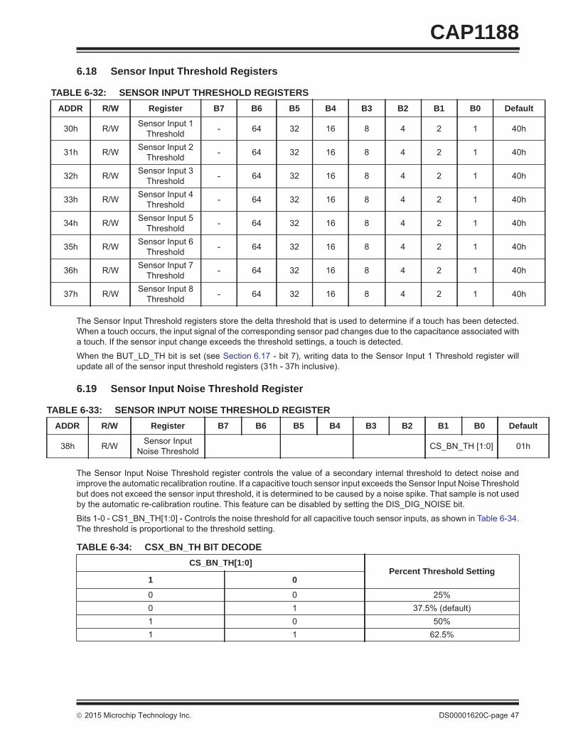
2015 Microchip Technology Inc. DS00001620C-page 47
CAP11886.18 Sensor Input Threshold Registers
The Sensor Input Threshold registers store the delta threshold that is used to determine if a touch has been detected.When a touch occurs, the input signal of the corresponding sensor pad changes due to the capacitance associated witha touch. If the sensor input change exceeds the threshold settings, a touch is detected.
When the BUT_LD_TH bit is set (see Section 6.17 - bit 7), writing data to the Sensor Input 1 Threshold register willupdate all of the sensor input threshold registers (31h - 37h inclusive).
6.19 Sensor Input Noise Threshold Register
The Sensor Input Noise Threshold register controls the value of a secondary internal threshold to detect noise andimprove the automatic recalibration routine. If a capacitive touch sensor input exceeds the Sensor Input Noise Thresholdbut does not exceed the sensor input threshold, it is determined to be caused by a noise spike. That sample is not usedby the automatic re-calibration routine. This feature can be disabled by setting the DIS_DIG_NOISE bit.
Bits 1-0 - CS1_BN_TH[1:0] - Controls the noise threshold for all capacitive touch sensor inputs, as shown in Table 6-34.The threshold is proportional to the threshold setting.
TABLE 6-32: SENSOR INPUT THRESHOLD REGISTERS ADDR R/W Register B7 B6 B5 B4 B3 B2 B1 B0 Default
30h R/W Sensor Input 1 Threshold - 64 32 16 8 4 2 1 40h
31h R/W Sensor Input 2 Threshold - 64 32 16 8 4 2 1 40h
32h R/W Sensor Input 3 Threshold - 64 32 16 8 4 2 1 40h
33h R/W Sensor Input 4 Threshold - 64 32 16 8 4 2 1 40h
34h R/W Sensor Input 5 Threshold - 64 32 16 8 4 2 1 40h
35h R/W Sensor Input 6 Threshold - 64 32 16 8 4 2 1 40h
36h R/W Sensor Input 7 Threshold - 64 32 16 8 4 2 1 40h
37h R/W Sensor Input 8 Threshold - 64 32 16 8 4 2 1 40h
TABLE 6-33: SENSOR INPUT NOISE THRESHOLD REGISTERADDR R/W Register B7 B6 B5 B4 B3 B2 B1 B0 Default
38h R/W Sensor Input Noise Threshold CS_BN_TH [1:0] 01h
TABLE 6-34: CSX_BN_TH BIT DECODE CS_BN_TH[1:0]
Percent Threshold Setting1 0
0 0 25%0 1 37.5% (default) 1 0 50%1 1 62.5%
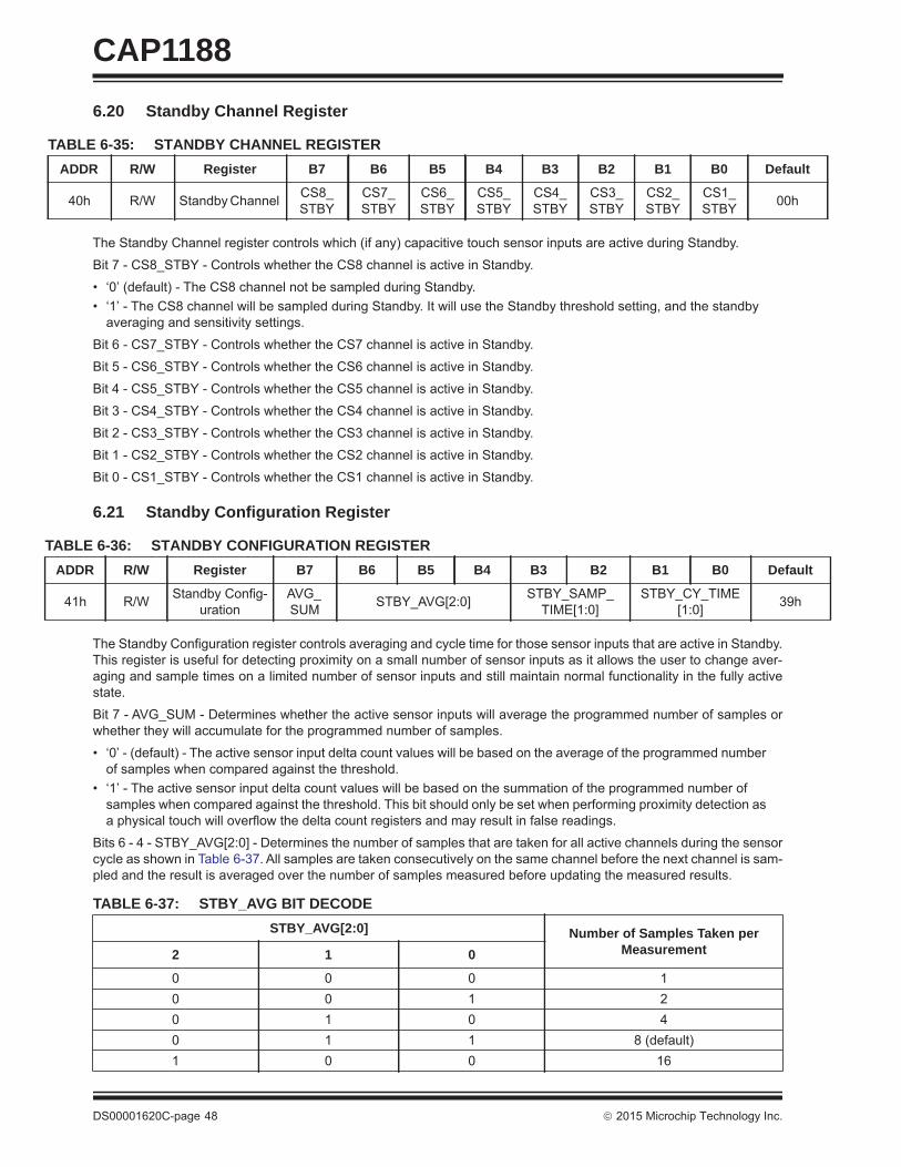
CAP1188
DS00001620C-page 48 2015 Microchip Technology Inc.
6.20 Standby Channel Register
The Standby Channel register controls which (if any) capacitive touch sensor inputs are active during Standby.
Bit 7 - CS8_STBY - Controls whether the CS8 channel is active in Standby.
• ‘0’ (default) - The CS8 channel not be sampled during Standby. • ‘1’ - The CS8 channel will be sampled during Standby. It will use the Standby threshold setting, and the standby
averaging and sensitivity settings.
Bit 6 - CS7_STBY - Controls whether the CS7 channel is active in Standby.
Bit 5 - CS6_STBY - Controls whether the CS6 channel is active in Standby.
Bit 4 - CS5_STBY - Controls whether the CS5 channel is active in Standby.
Bit 3 - CS4_STBY - Controls whether the CS4 channel is active in Standby.
Bit 2 - CS3_STBY - Controls whether the CS3 channel is active in Standby.
Bit 1 - CS2_STBY - Controls whether the CS2 channel is active in Standby.
Bit 0 - CS1_STBY - Controls whether the CS1 channel is active in Standby.
6.21 Standby Configuration Register
The Standby Configuration register controls averaging and cycle time for those sensor inputs that are active in Standby.This register is useful for detecting proximity on a small number of sensor inputs as it allows the user to change aver-aging and sample times on a limited number of sensor inputs and still maintain normal functionality in the fully activestate.
Bit 7 - AVG_SUM - Determines whether the active sensor inputs will average the programmed number of samples orwhether they will accumulate for the programmed number of samples.
• ‘0’ - (default) - The active sensor input delta count values will be based on the average of the programmed number of samples when compared against the threshold.
• ‘1’ - The active sensor input delta count values will be based on the summation of the programmed number of samples when compared against the threshold. This bit should only be set when performing proximity detection as a physical touch will overflow the delta count registers and may result in false readings.
Bits 6 - 4 - STBY_AVG[2:0] - Determines the number of samples that are taken for all active channels during the sensorcycle as shown in Table 6-37. All samples are taken consecutively on the same channel before the next channel is sam-pled and the result is averaged over the number of samples measured before updating the measured results.
TABLE 6-35: STANDBY CHANNEL REGISTERADDR R/W Register B7 B6 B5 B4 B3 B2 B1 B0 Default
40h R/W Standby Channel CS8_STBY
CS7_STBY
CS6_STBY
CS5_STBY
CS4_STBY
CS3_STBY
CS2_STBY
CS1_STBY 00h
TABLE 6-36: STANDBY CONFIGURATION REGISTERADDR R/W Register B7 B6 B5 B4 B3 B2 B1 B0 Default
41h R/W Standby Config-uration
AVG_SUM STBY_AVG[2:0] STBY_SAMP_
TIME[1:0]STBY_CY_TIME
[1:0] 39h
TABLE 6-37: STBY_AVG BIT DECODE STBY_AVG[2:0] Number of Samples Taken per
Measurement2 1 0
0 0 0 1 0 0 1 20 1 0 40 1 1 8 (default) 1 0 0 16
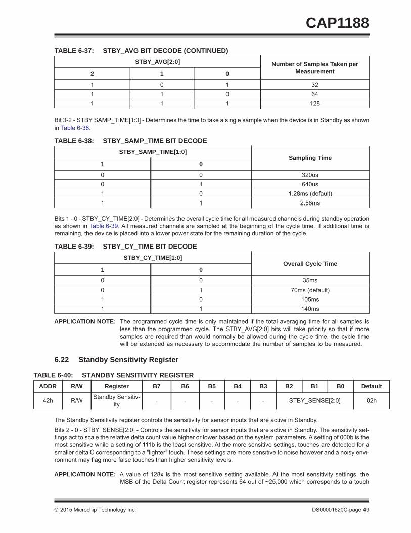
2015 Microchip Technology Inc. DS00001620C-page 49
CAP1188
Bit 3-2 - STBY SAMP_TIME[1:0] - Determines the time to take a single sample when the device is in Standby as shownin Table 6-38.
Bits 1 - 0 - STBY_CY_TIME[2:0] - Determines the overall cycle time for all measured channels during standby operationas shown in Table 6-39. All measured channels are sampled at the beginning of the cycle time. If additional time isremaining, the device is placed into a lower power state for the remaining duration of the cycle.
APPLICATION NOTE: The programmed cycle time is only maintained if the total averaging time for all samples isless than the programmed cycle. The STBY_AVG[2:0] bits will take priority so that if moresamples are required than would normally be allowed during the cycle time, the cycle timewill be extended as necessary to accommodate the number of samples to be measured.
6.22 Standby Sensitivity Register
The Standby Sensitivity register controls the sensitivity for sensor inputs that are active in Standby.
Bits 2 - 0 - STBY_SENSE[2:0] - Controls the sensitivity for sensor inputs that are active in Standby. The sensitivity set-tings act to scale the relative delta count value higher or lower based on the system parameters. A setting of 000b is themost sensitive while a setting of 111b is the least sensitive. At the more sensitive settings, touches are detected for asmaller delta C corresponding to a “lighter” touch. These settings are more sensitive to noise however and a noisy envi-ronment may flag more false touches than higher sensitivity levels.
APPLICATION NOTE: A value of 128x is the most sensitive setting available. At the most sensitivity settings, theMSB of the Delta Count register represents 64 out of ~25,000 which corresponds to a touch
1 0 1 321 1 0 641 1 1 128
TABLE 6-38: STBY_SAMP_TIME BIT DECODE STBY_SAMP_TIME[1:0]
Sampling Time1 0
0 0 320us0 1 640us 1 0 1.28ms (default)1 1 2.56ms
TABLE 6-39: STBY_CY_TIME BIT DECODE STBY_CY_TIME[1:0]
Overall Cycle Time1 0
0 0 35ms0 1 70ms (default) 1 0 105ms1 1 140ms
TABLE 6-40: STANDBY SENSITIVITY REGISTERADDR R/W Register B7 B6 B5 B4 B3 B2 B1 B0 Default
42h R/W Standby Sensitiv-ity - - - - - STBY_SENSE[2:0] 02h
TABLE 6-37: STBY_AVG BIT DECODE (CONTINUED) STBY_AVG[2:0] Number of Samples Taken per
Measurement2 1 0
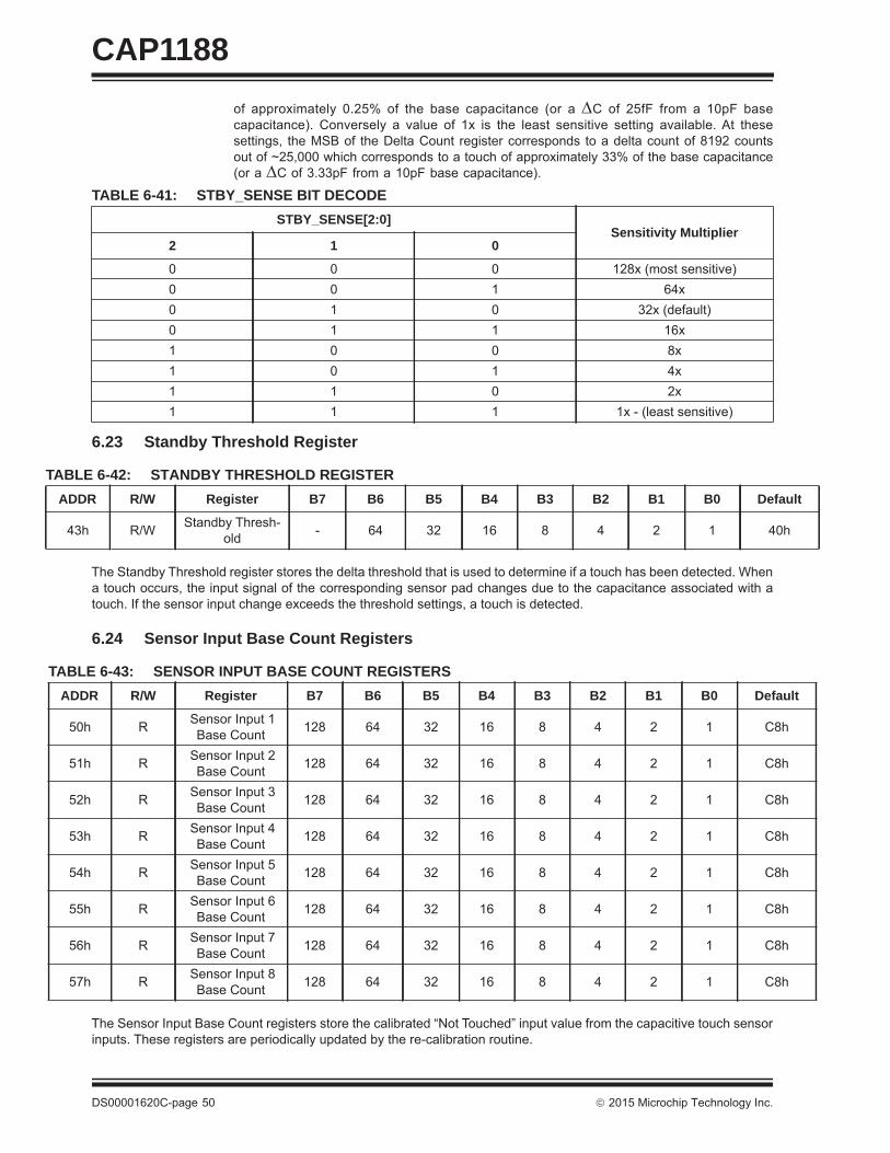
CAP1188
DS00001620C-page 50 2015 Microchip Technology Inc.
of approximately 0.25% of the base capacitance (or a C of 25fF from a 10pF basecapacitance). Conversely a value of 1x is the least sensitive setting available. At thesesettings, the MSB of the Delta Count register corresponds to a delta count of 8192 countsout of ~25,000 which corresponds to a touch of approximately 33% of the base capacitance(or a C of 3.33pF from a 10pF base capacitance).
6.23 Standby Threshold Register
The Standby Threshold register stores the delta threshold that is used to determine if a touch has been detected. Whena touch occurs, the input signal of the corresponding sensor pad changes due to the capacitance associated with atouch. If the sensor input change exceeds the threshold settings, a touch is detected.
6.24 Sensor Input Base Count Registers
The Sensor Input Base Count registers store the calibrated “Not Touched” input value from the capacitive touch sensorinputs. These registers are periodically updated by the re-calibration routine.
TABLE 6-41: STBY_SENSE BIT DECODE STBY_SENSE[2:0]
Sensitivity Multiplier2 1 0
0 0 0 128x (most sensitive)0 0 1 64x 0 1 0 32x (default) 0 1 1 16x1 0 0 8x1 0 1 4x1 1 0 2x1 1 1 1x - (least sensitive)
TABLE 6-42: STANDBY THRESHOLD REGISTERADDR R/W Register B7 B6 B5 B4 B3 B2 B1 B0 Default
43h R/W Standby Thresh-old - 64 32 16 8 4 2 1 40h
TABLE 6-43: SENSOR INPUT BASE COUNT REGISTERS ADDR R/W Register B7 B6 B5 B4 B3 B2 B1 B0 Default
50h R Sensor Input 1 Base Count 128 64 32 16 8 4 2 1 C8h
51h R Sensor Input 2 Base Count 128 64 32 16 8 4 2 1 C8h
52h R Sensor Input 3 Base Count 128 64 32 16 8 4 2 1 C8h
53h R Sensor Input 4 Base Count 128 64 32 16 8 4 2 1 C8h
54h R Sensor Input 5 Base Count 128 64 32 16 8 4 2 1 C8h
55h R Sensor Input 6 Base Count 128 64 32 16 8 4 2 1 C8h
56h R Sensor Input 7 Base Count 128 64 32 16 8 4 2 1 C8h
57h R Sensor Input 8 Base Count 128 64 32 16 8 4 2 1 C8h
2015 Microchip Technology Inc. DS00001620C-page 51
CAP1188The routine uses an internal adder to add the current count value for each reading to the sum of the previous readingsuntil sample size has been reached. At this point, the upper 16 bits are taken and used as the Sensor Input Base Count.The internal adder is then reset and the re-calibration routine continues.
The data presented is determined by the BASE_SHIFT[3:0] bits (see Section 6.5).
6.25 LED Output Type Register
The LED Output Type register controls the type of output for the LED pins. Each pin is controlled by a single bit. Referto application note 21.4 CAP1188 Family LED Configuration Options for more information about implementing LEDs.
Bit 7 - LED8_OT - Determines the output type of the LED8 pin.
• ‘0’ (default) - The LED8 pin is an open-drain output with an external pull-up resistor. When the appropriate pin is set to the “active” state (logic ‘1’), the pin will be driven low. Conversely, when the pin is set to the “inactive” state (logic ‘0’), then the pin will be left in a High Z state and pulled high via an external pull-up resistor.
• ‘1’ - The LED8 pin is a push-pull output. When driving a logic ‘1’, the pin is driven high. When driving a logic ‘0’, the pin is driven low.
Bit 6 - LED7_OT - Determines the output type of the LED7 pin.
Bit 5 - LED6_OT - Determines the output type of the LED6 pin.
Bit 4 - LED5_OT - Determines the output type of the LED5 pin.
Bit 3 - LED4_OT - Determines the output type of the LED4 pin.
Bit 2 - LED3_OT - Determines the output type of the LED3 pin.
Bit 1 - LED2_OT - Determines the output type of the LED2 pin.
Bit 0 - LED1_OT - Determines the output type of the LED1 pin.
6.26 Sensor Input LED Linking Register
The Sensor Input LED Linking register controls whether a capacitive touch sensor input is linked to an LED output. Ifthe corresponding bit is set, then the appropriate LED output will change states defined by the LED Behavior controls(see Section 6.31) in response to the capacitive touch sensor input.
Bit 7 - CS8_LED8 - Links the LED8 output to a detected touch on the CS8 sensor input. When a touch is detected, theLED is actuated and will behave as determined by the LED Behavior controls.
• ‘0’ (default) - The LED8 output is not associated with the CS8 input. If a touch is detected on the CS8 input, then the LED will not automatically be actuated. The LED is enabled and controlled via the LED Output Control register (see Section 6.28) and the LED Behavior registers (see Section 6.31).
• ‘1’ - The LED8 output is associated with the CS8 input. If a touch is detected on the CS8 input, the LED will be actuated and behave as defined in Table 6-52.
Bit 6 - CS7_LED7 - Links the LED7 output to a detected touch on the CS7 sensor input. When a touch is detected, theLED is actuated and will behave as determined by the LED Behavior controls.
Bit 5 - CS6_LED6 - Links the LED6 output to a detected touch on the CS6 sensor input. When a touch is detected, theLED is actuated and will behave as determined by the LED Behavior controls.
Bit 4 - CS5_LED5 - Links the LED5 output to a detected touch on the CS5 sensor input. When a touch is detected, theLED is actuated and will behave as determined by the LED Behavior controls.
TABLE 6-44: LED OUTPUT TYPE REGISTERADDR R/W Register B7 B6 B5 B4 B3 B2 B1 B0 Default
71h R/W LED Output Type
LED8_OT
LED7_OT
LED6_OT
LED5_OT
LED4_OT
LED3_OT
LED2_OT
LED1_OT 00h
TABLE 6-45: SENSOR INPUT LED LINKING REGISTERADDR R/W Register B7 B6 B5 B4 B3 B2 B1 B0 Default
72h R/W Sensor Input LED Linking
CS8_LED8
CS7_LED7
CS6_LED6
CS5_LED5
CS4_LED4
CS3_LED3
CS2_LED2
CS1_LED1
00h
CAP1188
DS00001620C-page 52 2015 Microchip Technology Inc.
Bit 3 - CS4_LED4 - Links the LED4 output to a detected touch on the CS4 sensor input. When a touch is detected, theLED is actuated and will behave as determined by the LED Behavior controls.
Bit 2 - CS3_LED3 - Links the LED3 output to a detected touch on the CS3 sensor input. When a touch is detected, theLED is actuated and will behave as determined by the LED Behavior controls.
Bit 1 - CS2_LED2 - Links the LED2 output to a detected touch on the CS2 sensor input. When a touch is detected, theLED is actuated and will behave as determined by the LED Behavior controls.
Bit 0 - CS1_LED1 - Links the LED1 output to a detected touch on the CS1 sensor input. When a touch is detected, theLED is actuated and will behave as determined by the LED Behavior controls.
6.27 LED Polarity Register
The LED Polarity register controls the logical polarity of the LED outputs. When these bits are set or cleared, the corre-sponding LED Mirror controls are also set or cleared (unless the BLK_POL_MIR bit is set - see Section 6.6, "Configu-ration Registers"). Table 6-48, "LED Polarity Behavior" shows the interaction between the polarity controls, outputcontrols, and relative brightness.
APPLICATION NOTE: The polarity controls determine the final LED pin drive. A touch on a linked capacitive touchsensor input is treated in the same way as the LED Output Control bit being set to a logic ‘1’.
APPLICATION NOTE: The LED drive assumes that the LEDs are configured such that if the LED pin is driven toa logic ‘0’ then the LED will be on and that the CAP1188 LED pin is sinking the LED current.Conversely, if the LED pin is driven to a logic ‘1’, the LED will be off and there is no currentflow. See Figure 5-1, "System Diagram for CAP1188".
APPLICATION NOTE: This application note applies when the LED polarity is inverted (LEDx_POL = ‘0’). For LEDoperation, the duty cycle settings determine the % of time that the LED pin will be driven toa logic ‘0’ state in. The Max Duty Cycle settings define the maximum % of time that the LEDpin will be driven low (i.e. maximum % of time that the LED is on) while the Min Duty Cyclesettings determine the minimum % of time that the LED pin will be driven low (i.e. minimum% of time that the LED is on). When there is no touch detected or the LED Output Controlregister bit is at a logic ‘0’, the LED output will be driven at the minimum duty cycle setting.Breathe operations will ramp the duty cycle from the minimum duty cycle to the maximumduty cycle.
APPLICATION NOTE: This application note applies when the LED polarity is non-inverted (LEDx_POL = ‘1’). ForLED operation, the duty cycle settings determine the % of time that the LED pin will be drivento a logic ‘1’ state. The Max Duty Cycle settings define the maximum % of time that the LEDpin will be driven high (i.e. maximum % of time that the LED is off) while the Min Duty Cyclesettings determine the minimum % of time that the LED pin will be driven high (i.e. minimum% of time that the LED is off). When there is no touch detected or the LED Output Controlregister bit is at a logic ‘0’, the LED output will be driven at 100 minus the minimum dutycycle setting. Breathe operations will ramp the duty cycle from 100 minus the minimum dutycycle to 100 minus the maximum duty cycle.
APPLICATION NOTE: The LED Mirror controls (see Section 6.30, "LED Mirror Control Register") work with thepolarity controls with respect to LED brightness but will not have a direct effect on the outputpin drive.
TABLE 6-46: LED POLARITY REGISTER ADDR R/W Register B7 B6 B5 B4 B3 B2 B1 B0 Default
73h R/W LED Polarity LED8_POL
LED7_POL
LED6_POL
LED5_POL
LED4_POL
LED3_POL
LED2_POL
LED1_POL 00h
2015 Microchip Technology Inc. DS00001620C-page 53
CAP1188Bit 7 - LED8_POL - Determines the polarity of the LED8 output.
• ‘0’ (default) - The LED8 output is inverted. For example, a setting of ‘1’ in the LED Output Control register will cause the LED pin output to be driven to a logic ‘0’.
• ‘1’ - The LED8 output is non-inverted. For example, a setting of ‘1’ in the LED Output Control register will cause the LED pin output to be driven to a logic ‘1’ or left in the high-z state as determined by its output type.
Bit 6 - LED7_POL - Determines the polarity of the LED7 output.
Bit 5 - LED6_POL - Determines the polarity of the LED6 output.
Bit 4 - LED5_POL - Determines the polarity of the LED5 output.
Bit 3 - LED4_POL - Determines the polarity of the LED4 output.
Bit 2 - LED3_POL - Determines the polarity of the LED3 output.
Bit 1 - LED2_POL - Determines the polarity of the LED2 output.
Bit 0 - LED1_POL - Determines the polarity of the LED1 output.
6.28 LED Output Control Register
The LED Output Control Register controls the output state of the LED pins that are not linked to sensor inputs.
The LED Polarity Control Register will determine the non actuated state of the LED pins. The actuated LED behavior isdetermined by the LED behavior controls (see Section 6.31, "LED Behavior Registers").
Table 6-48 shows the interaction between the polarity controls, output controls, and relative brightness.
Bit 7 - LED8_DR - Determines whether the LED8 output is driven high or low.
• ‘0’ (default) - The LED8 output is driven at the minimum duty cycle or not actuated. • ‘1’ - The LED8 output is driven at the maximum duty cycle or is actuated.
Bit 6 - LED7_DR - Determines whether LED7 output is driven high or low.
Bit 5 - LED6_DR - Determines whether LED6 output is driven high or low.
Bit 4 - LED5_DR - Determines whether LED5 output is driven high or low.
Bit 3 - LED4_DR - Determines whether LED4 output is driven high or low.
Bit 2 - LED3_DR - Determines whether LED3 output is driven high or low.
Bit 1 - LED2_DR - Determines whether LED2 output is driven high or low.
Bit 0 - LED1_DR - Determines whether LED1 output is driven high or low.
TABLE 6-47: LED OUTPUT CONTROL REGISTERADDR R/W Register B7 B6 B5 B4 B3 B2 B1 B0 Default
74h R/W LED Output Control
LED8_DR
LED7_DR
LED6_DR
LED5_DR
LED4_DR
LED3_DR
LED2_DR
LED1_DR 00h
Note: If an LED is linked to a sensor input in the Sensor Input LED Linking Register (Section 6.26, "Sensor InputLED Linking Register"), the corresponding bit in the LED Output Control Register is ignored (i.e. a linkedLED cannot be host controlled).
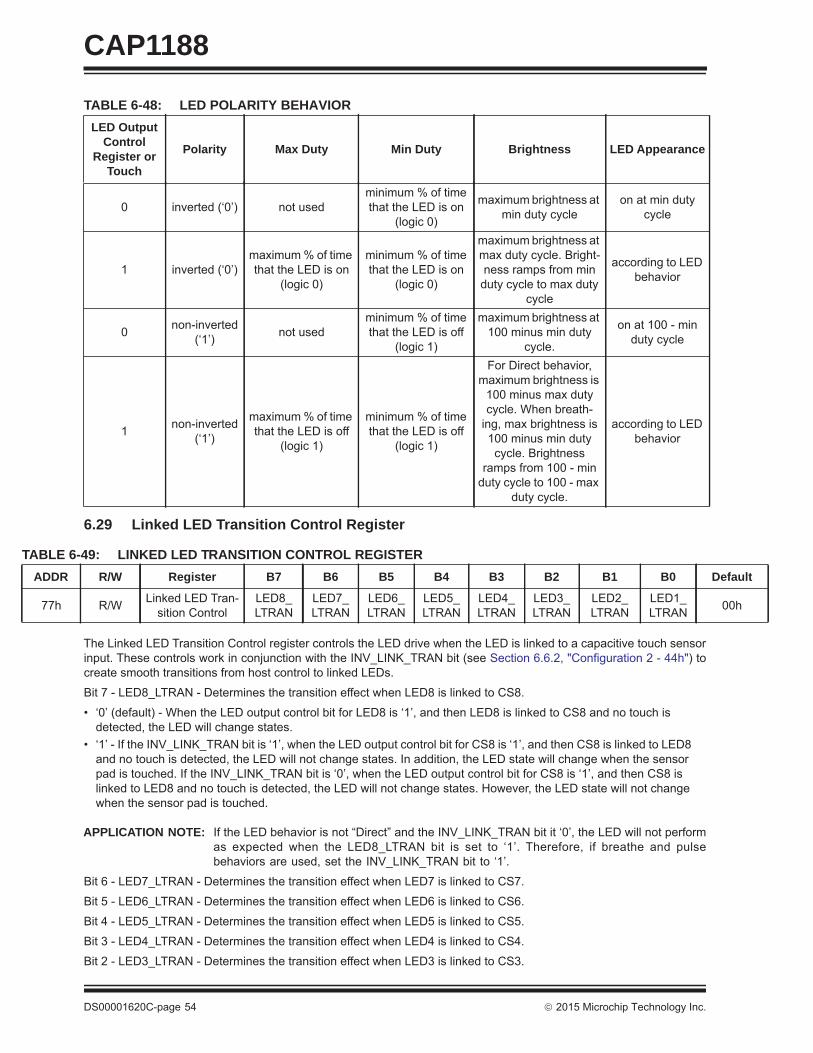
CAP1188
DS00001620C-page 54 2015 Microchip Technology Inc.
6.29 Linked LED Transition Control Register
The Linked LED Transition Control register controls the LED drive when the LED is linked to a capacitive touch sensorinput. These controls work in conjunction with the INV_LINK_TRAN bit (see Section 6.6.2, "Configuration 2 - 44h") tocreate smooth transitions from host control to linked LEDs.
Bit 7 - LED8_LTRAN - Determines the transition effect when LED8 is linked to CS8.
• ‘0’ (default) - When the LED output control bit for LED8 is ‘1’, and then LED8 is linked to CS8 and no touch is detected, the LED will change states.
• ‘1’ - If the INV_LINK_TRAN bit is ‘1’, when the LED output control bit for CS8 is ‘1’, and then CS8 is linked to LED8 and no touch is detected, the LED will not change states. In addition, the LED state will change when the sensor pad is touched. If the INV_LINK_TRAN bit is ‘0’, when the LED output control bit for CS8 is ‘1’, and then CS8 is linked to LED8 and no touch is detected, the LED will not change states. However, the LED state will not change when the sensor pad is touched.
APPLICATION NOTE: If the LED behavior is not “Direct” and the INV_LINK_TRAN bit it ‘0’, the LED will not performas expected when the LED8_LTRAN bit is set to ‘1’. Therefore, if breathe and pulsebehaviors are used, set the INV_LINK_TRAN bit to ‘1’.
Bit 6 - LED7_LTRAN - Determines the transition effect when LED7 is linked to CS7.
Bit 5 - LED6_LTRAN - Determines the transition effect when LED6 is linked to CS6.
Bit 4 - LED5_LTRAN - Determines the transition effect when LED5 is linked to CS5.
Bit 3 - LED4_LTRAN - Determines the transition effect when LED4 is linked to CS4.
Bit 2 - LED3_LTRAN - Determines the transition effect when LED3 is linked to CS3.
TABLE 6-48: LED POLARITY BEHAVIOR LED Output
Control Register or
Touch
Polarity Max Duty Min Duty Brightness LED Appearance
0 inverted (‘0’) not usedminimum % of time that the LED is on
(logic 0)
maximum brightness at min duty cycle
on at min duty cycle
1 inverted (‘0’)maximum % of time that the LED is on
(logic 0)
minimum % of time that the LED is on
(logic 0)
maximum brightness at max duty cycle. Bright-ness ramps from min
duty cycle to max duty cycle
according to LED behavior
0 non-inverted (‘1’) not used
minimum % of time that the LED is off
(logic 1)
maximum brightness at 100 minus min duty
cycle.
on at 100 - min duty cycle
1 non-inverted (‘1’)
maximum % of time that the LED is off
(logic 1)
minimum % of time that the LED is off
(logic 1)
For Direct behavior, maximum brightness is
100 minus max duty cycle. When breath-
ing, max brightness is 100 minus min duty
cycle. Brightness ramps from 100 - min
duty cycle to 100 - max duty cycle.
according to LED behavior
TABLE 6-49: LINKED LED TRANSITION CONTROL REGISTER ADDR R/W Register B7 B6 B5 B4 B3 B2 B1 B0 Default
77h R/W Linked LED Tran-sition Control
LED8_LTRAN
LED7_LTRAN
LED6_LTRAN
LED5_LTRAN
LED4_LTRAN
LED3_LTRAN
LED2_LTRAN
LED1_LTRAN 00h
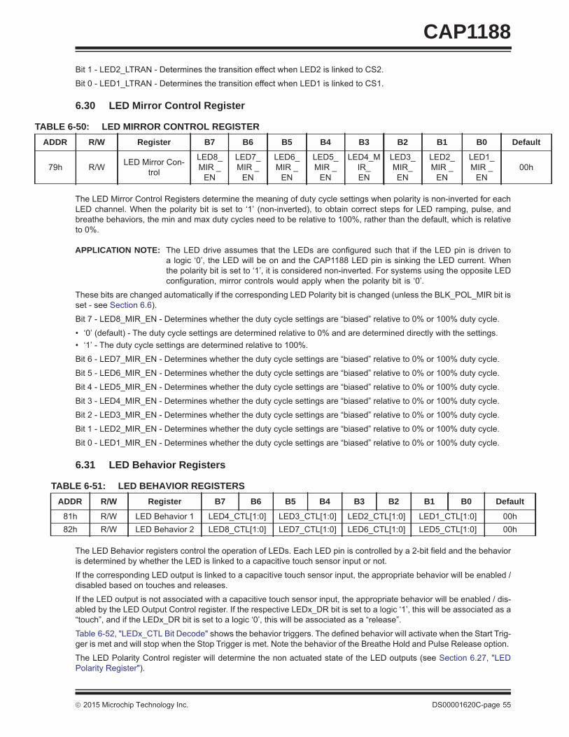
2015 Microchip Technology Inc. DS00001620C-page 55
CAP1188Bit 1 - LED2_LTRAN - Determines the transition effect when LED2 is linked to CS2.
Bit 0 - LED1_LTRAN - Determines the transition effect when LED1 is linked to CS1.
6.30 LED Mirror Control Register
The LED Mirror Control Registers determine the meaning of duty cycle settings when polarity is non-inverted for eachLED channel. When the polarity bit is set to ‘1’ (non-inverted), to obtain correct steps for LED ramping, pulse, andbreathe behaviors, the min and max duty cycles need to be relative to 100%, rather than the default, which is relativeto 0%.
APPLICATION NOTE: The LED drive assumes that the LEDs are configured such that if the LED pin is driven toa logic ‘0’, the LED will be on and the CAP1188 LED pin is sinking the LED current. Whenthe polarity bit is set to ‘1’, it is considered non-inverted. For systems using the opposite LEDconfiguration, mirror controls would apply when the polarity bit is ‘0’.
These bits are changed automatically if the corresponding LED Polarity bit is changed (unless the BLK_POL_MIR bit isset - see Section 6.6).
Bit 7 - LED8_MIR_EN - Determines whether the duty cycle settings are “biased” relative to 0% or 100% duty cycle.
• ‘0’ (default) - The duty cycle settings are determined relative to 0% and are determined directly with the settings. • ‘1’ - The duty cycle settings are determined relative to 100%.
Bit 6 - LED7_MIR_EN - Determines whether the duty cycle settings are “biased” relative to 0% or 100% duty cycle.
Bit 5 - LED6_MIR_EN - Determines whether the duty cycle settings are “biased” relative to 0% or 100% duty cycle.
Bit 4 - LED5_MIR_EN - Determines whether the duty cycle settings are “biased” relative to 0% or 100% duty cycle.
Bit 3 - LED4_MIR_EN - Determines whether the duty cycle settings are “biased” relative to 0% or 100% duty cycle.
Bit 2 - LED3_MIR_EN - Determines whether the duty cycle settings are “biased” relative to 0% or 100% duty cycle.
Bit 1 - LED2_MIR_EN - Determines whether the duty cycle settings are “biased” relative to 0% or 100% duty cycle.
Bit 0 - LED1_MIR_EN - Determines whether the duty cycle settings are “biased” relative to 0% or 100% duty cycle.
6.31 LED Behavior Registers
The LED Behavior registers control the operation of LEDs. Each LED pin is controlled by a 2-bit field and the behavioris determined by whether the LED is linked to a capacitive touch sensor input or not.
If the corresponding LED output is linked to a capacitive touch sensor input, the appropriate behavior will be enabled /disabled based on touches and releases.
If the LED output is not associated with a capacitive touch sensor input, the appropriate behavior will be enabled / dis-abled by the LED Output Control register. If the respective LEDx_DR bit is set to a logic ‘1’, this will be associated as a“touch”, and if the LEDx_DR bit is set to a logic ‘0’, this will be associated as a “release”.
Table 6-52, "LEDx_CTL Bit Decode" shows the behavior triggers. The defined behavior will activate when the Start Trig-ger is met and will stop when the Stop Trigger is met. Note the behavior of the Breathe Hold and Pulse Release option.
The LED Polarity Control register will determine the non actuated state of the LED outputs (see Section 6.27, "LEDPolarity Register").
TABLE 6-50: LED MIRROR CONTROL REGISTER ADDR R/W Register B7 B6 B5 B4 B3 B2 B1 B0 Default
79h R/W LED Mirror Con-trol
LED8_MIR _
EN
LED7_MIR _
EN
LED6_MIR _
EN
LED5_MIR _
EN
LED4_MIR_EN
LED3_MIR_EN
LED2_ MIR _
EN
LED1_MIR _
EN00h
TABLE 6-51: LED BEHAVIOR REGISTERSADDR R/W Register B7 B6 B5 B4 B3 B2 B1 B0 Default
81h R/W LED Behavior 1 LED4_CTL[1:0] LED3_CTL[1:0] LED2_CTL[1:0] LED1_CTL[1:0] 00h82h R/W LED Behavior 2 LED8_CTL[1:0] LED7_CTL[1:0] LED6_CTL[1:0] LED5_CTL[1:0] 00h
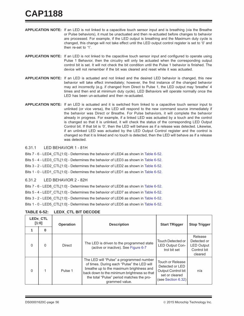
CAP1188
DS00001620C-page 56 2015 Microchip Technology Inc.
APPLICATION NOTE: If an LED is not linked to a capacitive touch sensor input and is breathing (via the Breatheor Pulse behaviors), it must be unactuated and then re-actuated before changes to behaviorare processed. For example, if the LED output is breathing and the Maximum duty cycle ischanged, this change will not take effect until the LED output control register is set to ‘0’ andthen re-set to ‘1’.
APPLICATION NOTE: If an LED is not linked to the capacitive touch sensor input and configured to operate usingPulse 1 Behavior, then the circuitry will only be actuated when the corresponding outputcontrol bit is set. It will not check the bit condition until the Pulse 1 behavior is finished. Thedevice will not remember if the bit was cleared and reset while it was actuated.
APPLICATION NOTE: If an LED is actuated and not linked and the desired LED behavior is changed, this newbehavior will take effect immediately; however, the first instance of the changed behaviormay act incorrectly (e.g. if changed from Direct to Pulse 1, the LED output may ‘breathe’ 4times and then end at minimum duty cycle). LED Behaviors will operate normally once theLED has been un-actuated and then re-actuated.
APPLICATION NOTE: If an LED is actuated and it is switched from linked to a capacitive touch sensor input tounlinked (or vice versa), the LED will respond to the new command source immediately ifthe behavior was Direct or Breathe. For Pulse behaviors, it will complete the behavioralready in progress. For example, if a linked LED was actuated by a touch and the controlis changed so that it is unlinked, it will check the status of the corresponding LED OutputControl bit. If that bit is ‘0’, then the LED will behave as if a release was detected. Likewise,if an unlinked LED was actuated by the LED Output Control register and the control ischanged so that it is linked and no touch is detected, then the LED will behave as if a releasewas detected.
6.31.1 LED BEHAVIOR 1 - 81HBits 7 - 6 - LED4_CTL[1:0] - Determines the behavior of LED4 as shown in Table 6-52.
Bits 5 - 4 - LED3_CTL[1:0] - Determines the behavior of LED3 as shown in Table 6-52.
Bits 3 - 2 - LED2_CTL[1:0] - Determines the behavior of LED2 as shown in Table 6-52.
Bits 1 - 0 - LED1_CTL[1:0] - Determines the behavior of LED1 as shown in Table 6-52.
6.31.2 LED BEHAVIOR 2 - 82HBits 7 - 6 - LED8_CTL[1:0] - Determines the behavior of LED8 as shown in Table 6-52.
Bits 5 - 4 - LED7_CTL[1:0] - Determines the behavior of LED7 as shown in Table 6-52.
Bits 3 - 2 - LED6_CTL[1:0] - Determines the behavior of LED6 as shown in Table 6-52.
Bits 1 - 0 - LED5_CTL[1:0] - Determines the behavior of LED5 as shown in Table 6-52.
TABLE 6-52: LEDX_CTL BIT DECODE LEDx_CTL
[1:0] Operation Description Start TRigger Stop Trigger1 0
0 0 Direct The LED is driven to the programmed state (active or inactive). See Figure 6-7
Touch Detected or LED Output Con-
trol bit set
Release Detected or LED Output Control bit
cleared
0 1 Pulse 1
The LED will “Pulse” a programmed number of times. During each “Pulse” the LED will
breathe up to the maximum brightness and back down to the minimum brightness so that
the total “Pulse” period matches the pro-grammed value.
Touch or Release Detected or LED Output Control bit
set or cleared (see Section 6.32)
n/a
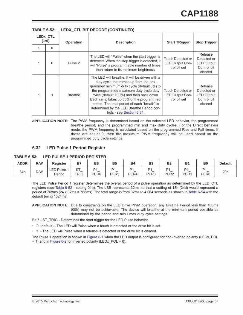
2015 Microchip Technology Inc. DS00001620C-page 57
CAP1188
APPLICATION NOTE: The PWM frequency is determined based on the selected LED behavior, the programmedbreathe period, and the programmed min and max duty cycles. For the Direct behaviormode, the PWM frequency is calculated based on the programmed Rise and Fall times. Ifthese are set at 0, then the maximum PWM frequency will be used based on theprogrammed duty cycle settings.
6.32 LED Pulse 1 Period Register
The LED Pulse Period 1 register determines the overall period of a pulse operation as determined by the LED_CTLregisters (see Table 6-52 - setting 01b). The LSB represents 32ms so that a setting of 18h (24d) would represent aperiod of 768ms (24 x 32ms = 768ms). The total range is from 32ms to 4.064 seconds as shown in Table 6-54 with thedefault being 1024ms.
APPLICATION NOTE: Due to constraints on the LED Drive PWM operation, any Breathe Period less than 160ms(05h) may not be achievable. The device will breathe at the minimum period possible asdetermined by the period and min / max duty cycle settings.
Bit 7 - ST_TRIG - Determines the start trigger for the LED Pulse behavior.
• ‘0’ (default) - The LED will Pulse when a touch is detected or the drive bit is set.• ‘1’ - The LED will Pulse when a release is detected or the drive bit is cleared.
The Pulse 1 operation is shown in Figure 6-1 when the LED output is configured for non-inverted polarity (LEDx_POL= 1) and in Figure 6-2 for inverted polarity (LEDx_POL = 0).
1 0 Pulse 2
The LED will “Pulse” when the start trigger is detected. When the stop trigger is detected, it will “Pulse” a programmable number of times
then return to its minimum brightness.
Touch Detected or LED Output Con-
trol bit set
Release Detected or LED Output Control bit
cleared
1 1 Breathe
The LED will breathe. It will be driven with a duty cycle that ramps up from the pro-
grammed minimum duty cycle (default 0%) to the programmed maximum duty cycle duty cycle (default 100%) and then back down.
Each ramp takes up 50% of the programmed period. The total period of each “breath” is
determined by the LED Breathe Period con-trols - see Section 6.34.
Touch Detected or LED Output Con-
trol bit set
Release Detected or LED Output Control bit
cleared
TABLE 6-53: LED PULSE 1 PERIOD REGISTERADDR R/W Register B7 B6 B5 B4 B3 B2 B1 B0 Default
84h R/W LED Pulse 1 Period
ST_TRIG
P1_PER6
P1_PER5
P1_PER4
P1_PER3
P1_PER2
P1_PER1
P1_PER0 20h
TABLE 6-52: LEDX_CTL BIT DECODE (CONTINUED) LEDx_CTL
[1:0] Operation Description Start TRigger Stop Trigger1 0
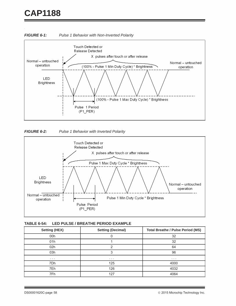
CAP1188
DS00001620C-page 58 2015 Microchip Technology Inc.
.
FIGURE 6-1: Pulse 1 Behavior with Non-Inverted Polarity
FIGURE 6-2: Pulse 1 Behavior with Inverted Polarity
TABLE 6-54: LED PULSE / BREATHE PERIOD EXAMPLE Setting (HEX) Setting (Decimal) Total Breathe / Pulse Period (MS)
00h 0 3201h 1 3202h 2 6403h 3 96. . . . . . . . . 7Dh 125 40007Eh 126 40327Fh 127 4064
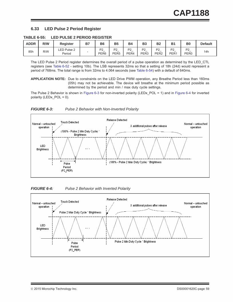
2015 Microchip Technology Inc. DS00001620C-page 59
CAP11886.33 LED Pulse 2 Period Register
The LED Pulse 2 Period register determines the overall period of a pulse operation as determined by the LED_CTLregisters (see Table 6-52 - setting 10b). The LSB represents 32ms so that a setting of 18h (24d) would represent aperiod of 768ms. The total range is from 32ms to 4.064 seconds (see Table 6-54) with a default of 640ms.
APPLICATION NOTE: Due to constraints on the LED Drive PWM operation, any Breathe Period less than 160ms(05h) may not be achievable. The device will breathe at the minimum period possible asdetermined by the period and min / max duty cycle settings.
The Pulse 2 Behavior is shown in Figure 6-3 for non-inverted polarity (LEDx_POL = 1) and in Figure 6-4 for invertedpolarity (LEDx_POL = 0).
TABLE 6-55: LED PULSE 2 PERIOD REGISTER ADDR R/W Register B7 B6 B5 B4 B3 B2 B1 B0 Default
85h R/W LED Pulse 2 Period - P2_
PER6P2_
PER5P2_
PER4P2_
PER3P2_
PER2P2_
PER1P2_
PER0 14h
FIGURE 6-3: Pulse 2 Behavior with Non-Inverted Polarity
FIGURE 6-4: Pulse 2 Behavior with Inverted Polarity
CAP1188
DS00001620C-page 60 2015 Microchip Technology Inc.
6.34 LED Breathe Period Register
The LED Breathe Period register determines the overall period of a breathe operation as determined by the LED_CTLregisters (see Table 6-52 - setting 11b). The LSB represents 32ms so that a setting of 18h (24d) would represent aperiod of 768ms. The total range is from 32ms to 4.064 seconds (see Table 6-54) with a default of 2976ms.
APPLICATION NOTE: Due to constraints on the LED Drive PWM operation, any Breathe Period less than 160ms(05h) may not be achievable. The device will breathe at the minimum period possible asdetermined by the period and min / max duty cycle settings.
6.35 LED Configuration Register
The LED Configuration register controls general LED behavior as well as the number of pulses that are sent for thePULSE LED output behavior.
Bit 6 - RAMP_ALERT - Determines whether the device will assert the ALERT# pin when LEDs actuated by the LEDOutput Control register bits have finished their respective behaviors. Interrupts will only be generated if the LED activityis generated by writing the LED Output Control registers. Any LED activity associated with touch detection will not causean interrupt to be generated when the LED behavior has been finished.
• ‘0’ (default) - The ALERT# pin will not be asserted when LEDs actuated by the LED Output Control register have finished their programmed behaviors.
• ‘1’ - The ALERT# pin will be asserted whenever any LED that is actuated by the LED Output Control register has finished its programmed behavior.
Bits 5 - 3 - PULSE2_CNT[2:0] - Determines the number of pulses used for the Pulse 2 behavior as shown in Table 6-58.
Bits 2 - 0 - PULSE1_CNT[2:0] - Determines the number of pulses used for the Pulse 1 behavior as shown in Table 6-58.
TABLE 6-56: LED BREATHE PERIOD REGISTERADDR R/W Register B7 B6 B5 B4 B3 B2 B1 B0 Default
86h R/W LED Breathe Period - BR_
PER6BR_
PER5BR_
PER4BR_
PER3BR_
PER2BR_
PER1BR_
PER0 5Dh
TABLE 6-57: LED CONFIGURATION REGISTERADDR R/W Register B7 B6 B5 B4 B3 B2 B1 B0 Default
88h R/W LED Config - RAMP_ALERT PULSE2_CNT[2:0] PULSE1_CNT[2:0] 04h
TABLE 6-58: PULSEX_CNT DECODE PULSEX_CNT[2:0]
Number of Breaths2 1 0
0 0 0 1 (default - Pulse 2)0 0 1 20 1 0 30 1 1 41 0 0 5 (default - Pulse 1)1 0 1 61 1 0 71 1 1 8
2015 Microchip Technology Inc. DS00001620C-page 61
CAP11886.36 LED Duty Cycle Registers
The LED Duty Cycle registers determine the minimum and maximum duty cycle settings used for the LED for each LEDbehavior. These settings affect the brightness of the LED when it is fully off and fully on.
The LED driver duty cycle will ramp up from the minimum duty cycle to the maximum duty cycle and back down again.
APPLICATION NOTE: When operating in Direct behavior mode, changes to the Duty Cycle settings will be appliedimmediately. When operating in Breathe, Pulse 1, or Pulse 2 modes, the LED must beunactuated and then re-actuated before changes to behavior are processed.
Bits 7 - 4 - X_MAX_DUTY[3:0] - Determines the maximum PWM duty cycle for the LED drivers as shown in Table 6-60.
Bits 3 - 0 - X_MIN_DUTY[3:0] - Determines the minimum PWM duty cycle for the LED drivers as shown in Table 6-60.
6.37 LED Direct Ramp Rates Register
TABLE 6-59: LED DUTY CYCLE REGISTERS ADDR R/W Register B7 B6 B5 B4 B3 B2 B1 B0 Default
90h R/W LED Pulse 1 Duty Cycle P1_MAX_DUTY[3:0] P1_MIN_DUTY[3:0] F0h
91h R/W LED Pulse 2 Duty Cycle P2_MAX_DUTY[3:0] P2_MIN_DUTY[3:0] F0h
92h R/W LED Breathe Duty Cycle BR_MAX_DUTY[3:0] BR_MIN_DUTY[3:0] F0h
93h R/W Direct Duty Cycle DR_MAX_DUTY[3:0] DR_MIN_DUTY[3:0] F0h
TABLE 6-60: LED DUTY CYCLE DECODE x_MAX/MIN_Duty [3:0]
Maximum Duty Cycle Minimum Duty Cycle3 2 1 0
0 0 0 0 7% 0%0 0 0 1 9% 7%0 0 1 0 11% 9%0 0 1 1 14% 11%0 1 0 0 17% 14%0 1 0 1 20% 17%0 1 1 0 23% 20%0 1 1 1 26% 23%1 0 0 0 30% 26%1 0 0 1 35% 30%1 0 1 0 40% 35%1 0 1 1 46% 40%1 1 0 0 53% 46%1 1 0 1 63% 53%1 1 1 0 77% 63%1 1 1 1 100% 77%
TABLE 6-61: LED DIRECT RAMP RATES REGISTERADDR R/W Register B7 B6 B5 B4 B3 B2 B1 B0 Default
94h R/W LED Direct Ramp Rates - - RISE_RATE[2:0] FALL_RATE[2:0] 00h
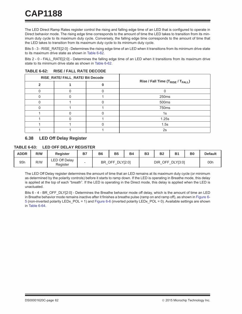
CAP1188
DS00001620C-page 62 2015 Microchip Technology Inc.
The LED Direct Ramp Rates register control the rising and falling edge time of an LED that is configured to operate inDirect behavior mode. The rising edge time corresponds to the amount of time the LED takes to transition from its min-imum duty cycle to its maximum duty cycle. Conversely, the falling edge time corresponds to the amount of time thatthe LED takes to transition from its maximum duty cycle to its minimum duty cycle.
Bits 5 - 3 - RISE_RATE[2:0] - Determines the rising edge time of an LED when it transitions from its minimum drive stateto its maximum drive state as shown in Table 6-62.
Bits 2 - 0 - FALL_RATE[2:0] - Determines the falling edge time of an LED when it transitions from its maximum drivestate to its minimum drive state as shown in Table 6-62.
6.38 LED Off Delay Register
The LED Off Delay register determines the amount of time that an LED remains at its maximum duty cycle (or minimumas determined by the polarity controls) before it starts to ramp down. If the LED is operating in Breathe mode, this delayis applied at the top of each “breath”. If the LED is operating in the Direct mode, this delay is applied when the LED isunactuated.
Bits 6 - 4 - BR_OFF_DLY[2:0] - Determines the Breathe behavior mode off delay, which is the amount of time an LEDin Breathe behavior mode remains inactive after it finishes a breathe pulse (ramp on and ramp off), as shown in Figure 6-5 (non-inverted polarity LEDx_POL = 1) and Figure 6-6 (inverted polarity LEDx_POL = 0). Available settings are shownin Table 6-64.
TABLE 6-62: RISE / FALL RATE DECODE RISE_RATE/ FALL_RATE/ Bit Decode
Rise / Fall Time (TRISE / TFALL)2 1 0
0 0 0 00 0 1 250ms0 1 0 500ms0 1 1 750ms1 0 0 1s1 0 1 1.25s1 1 0 1.5s1 1 1 2s
TABLE 6-63: LED OFF DELAY REGISTERADDR R/W Register B7 B6 B5 B4 B3 B2 B1 B0 Default
95h R/W LED Off Delay Register - BR_OFF_DLY[2:0] DIR_OFF_DLY[3:0] 00h
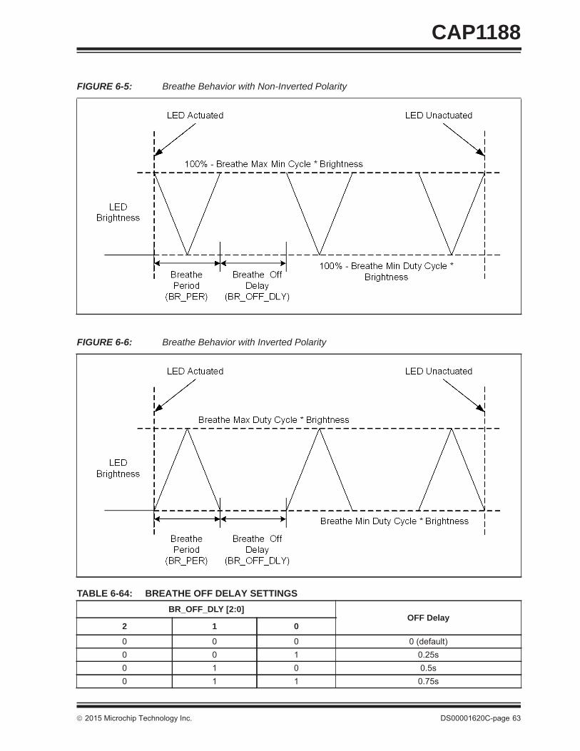
2015 Microchip Technology Inc. DS00001620C-page 63
CAP1188
FIGURE 6-5: Breathe Behavior with Non-Inverted Polarity
FIGURE 6-6: Breathe Behavior with Inverted Polarity
TABLE 6-64: BREATHE OFF DELAY SETTINGS BR_OFF_DLY [2:0]
OFF Delay2 1 0
0 0 0 0 (default)0 0 1 0.25s0 1 0 0.5s0 1 1 0.75s
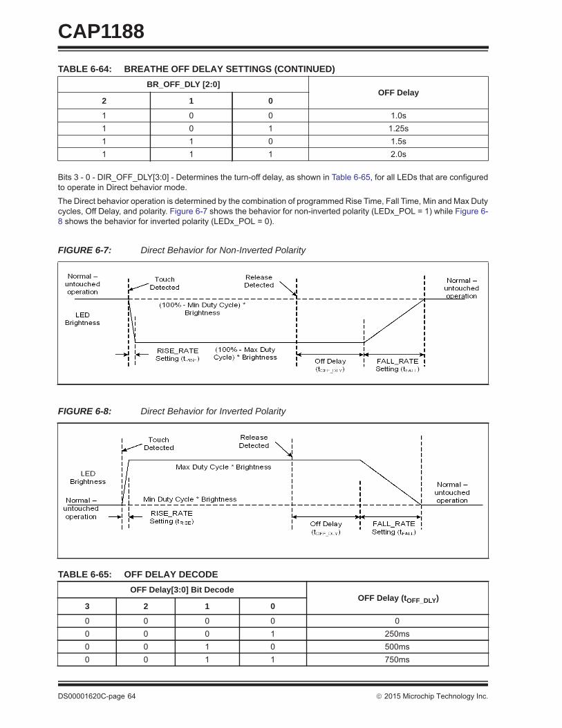
CAP1188
DS00001620C-page 64 2015 Microchip Technology Inc.
Bits 3 - 0 - DIR_OFF_DLY[3:0] - Determines the turn-off delay, as shown in Table 6-65, for all LEDs that are configuredto operate in Direct behavior mode.
The Direct behavior operation is determined by the combination of programmed Rise Time, Fall Time, Min and Max Dutycycles, Off Delay, and polarity. Figure 6-7 shows the behavior for non-inverted polarity (LEDx_POL = 1) while Figure 6-8 shows the behavior for inverted polarity (LEDx_POL = 0).
1 0 0 1.0s1 0 1 1.25s1 1 0 1.5s1 1 1 2.0s
FIGURE 6-7: Direct Behavior for Non-Inverted Polarity
FIGURE 6-8: Direct Behavior for Inverted Polarity
TABLE 6-65: OFF DELAY DECODE OFF Delay[3:0] Bit Decode
OFF Delay (tOFF_DLY)3 2 1 0
0 0 0 0 00 0 0 1 250ms0 0 1 0 500ms0 0 1 1 750ms
TABLE 6-64: BREATHE OFF DELAY SETTINGS (CONTINUED) BR_OFF_DLY [2:0]
OFF Delay2 1 0
2015 Microchip Technology Inc. DS00001620C-page 65
CAP1188
6.39 Sensor Input Calibration Registers
The Sensor Input Calibration registers hold the 10-bit value that represents the last calibration value.
0 1 0 0 1s0 1 0 1 1.25s0 1 1 0 1.5s0 1 1 1 2s1 0 0 0 2.5s1 0 0 1 3.0s1 0 1 0 3.5s1 0 1 1 4.0s1 1 0 0 4.5s
All others 5.0s
TABLE 6-66: SENSOR INPUT CALIBRATION REGISTERSADDR Register R/W B7 B6 B5 B4 B3 B2 B1 B0 Default
B1h Sensor Input 1 Calibration R CAL1_9 CAL1_8 CAL1_7 CAL1_6 CAL1_5 CAL1_4 CAL1_3 CAL1_2 00h
B2h Sensor Input 2 Calibration R CAL2_9 CAL2_8 CAL2_7 CAL2_6 CAL2_5 CAL2_4 CAL2_3 CAL2_2 00h
B3h Sensor Input 3 Calibration R CAL3_9 CAL3_8 CAL3_7 CAL3_6 CAL3_5 CAL3_4 CAL3_3 CAL3_2 00h
B4h Sensor Input 4 Calibration R CAL4_9 CAL4_8 CAL4_7 CAL4_6 CAL4_5 CAL4_4 CAL4_3 CAL4_2 00h
B5h Sensor Input 5 Calibration R CAL5_9 CAL5_8 CAL5_7 CAL5_6 CAL5_5 CAL5_4 CAL5_3 CAL5_2 00h
B6h Sensor Input 6 Calibration R CAL6_9 CAL6_8 CAL6_7 CAL6_6 CAL6_5 CAL6_4 CAL6_3 CAL6_2 00h
B7h Sensor Input 7 Calibration R CAL7_9 CAL7_8 CAL7_7 CAL7_6 CAL7_5 CAL7_4 CAL7_3 CAL7_2 00h
B8h Sensor Input 8 Calibration R CAL8_9 CAL8_8 CAL8_7 CAL8_6 CAL8_5 CAL8_4 CAL8_3 CAL8_2 00h
B9hSensor Input
Calibration LSB 1
R CAL4_1 CAL4_0 CAL3_1 CAL3_0 CAL2_1 CAL2_0 CAL1_1 CAL1_0 00h
BAhSensor Input
Calibration LSB 2
R CAL8_1 CAL8_0 CAL7_1 CAL7_0 CAL6_1 CAL6_0 CAL5_1 CAL5_0 00h
TABLE 6-65: OFF DELAY DECODE (CONTINUED) OFF Delay[3:0] Bit Decode
OFF Delay (tOFF_DLY)3 2 1 0
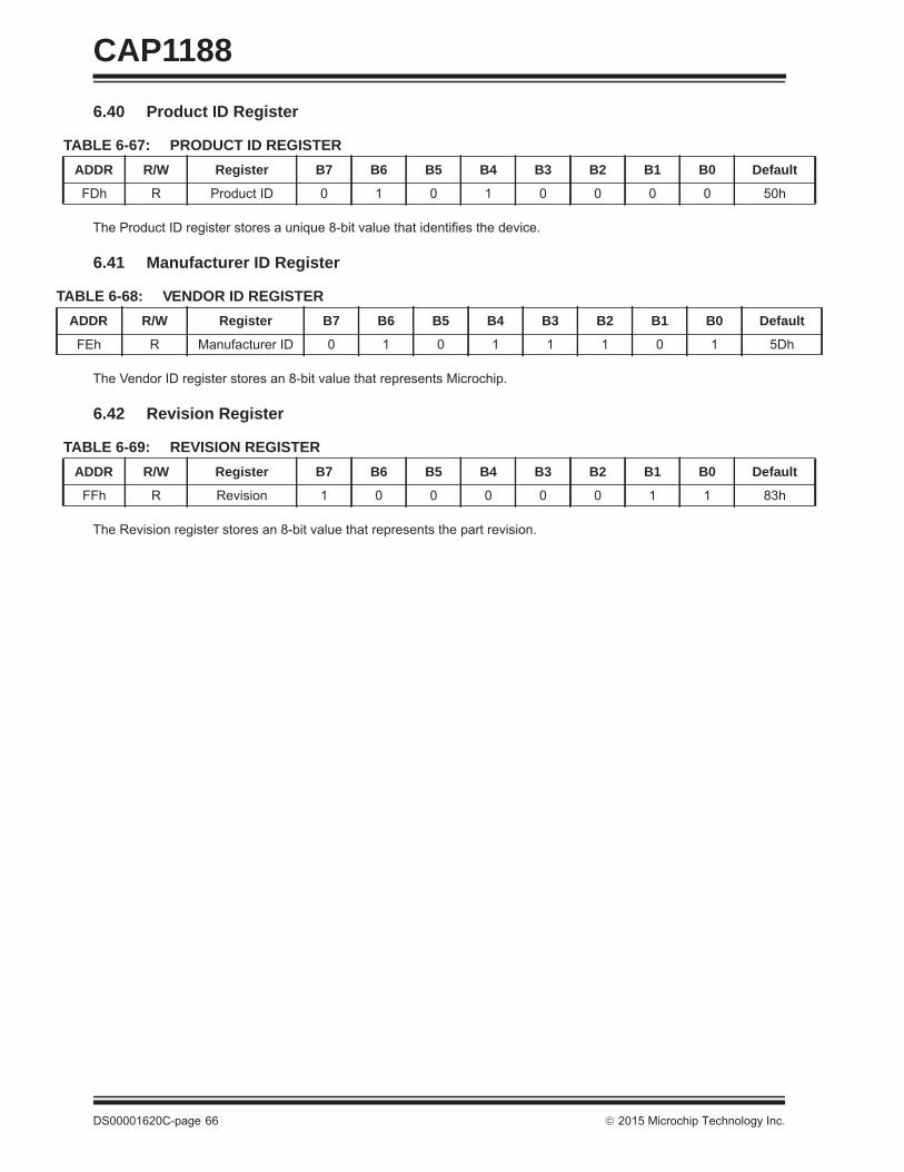
CAP1188
DS00001620C-page 66 2015 Microchip Technology Inc.
6.40 Product ID Register
The Product ID register stores a unique 8-bit value that identifies the device.
6.41 Manufacturer ID Register
The Vendor ID register stores an 8-bit value that represents Microchip.
6.42 Revision Register
The Revision register stores an 8-bit value that represents the part revision.
TABLE 6-67: PRODUCT ID REGISTER ADDR R/W Register B7 B6 B5 B4 B3 B2 B1 B0 Default
FDh R Product ID 0 1 0 1 0 0 0 0 50h
TABLE 6-68: VENDOR ID REGISTERADDR R/W Register B7 B6 B5 B4 B3 B2 B1 B0 Default
FEh R Manufacturer ID 0 1 0 1 1 1 0 1 5Dh
TABLE 6-69: REVISION REGISTERADDR R/W Register B7 B6 B5 B4 B3 B2 B1 B0 Default
FFh R Revision 1 0 0 0 0 0 1 1 83h
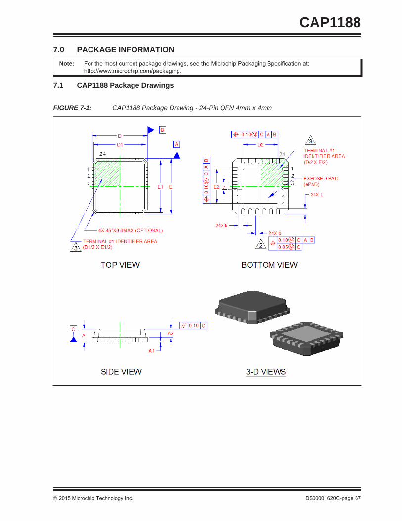
2015 Microchip Technology Inc. DS00001620C-page 67
CAP11887.0 PACKAGE INFORMATION
7.1 CAP1188 Package Drawings
Note: For the most current package drawings, see the Microchip Packaging Specification at: http://www.microchip.com/packaging.
FIGURE 7-1: CAP1188 Package Drawing - 24-Pin QFN 4mm x 4mm
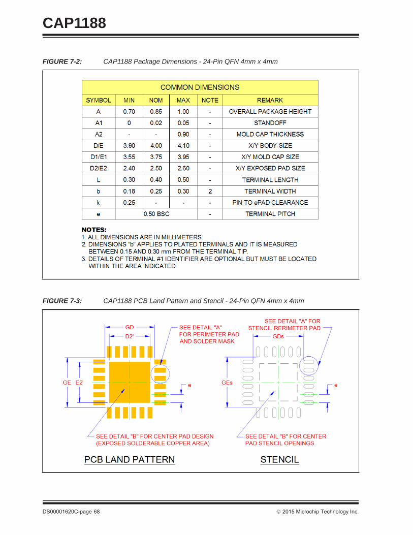
CAP1188
DS00001620C-page 68 2015 Microchip Technology Inc.
FIGURE 7-2: CAP1188 Package Dimensions - 24-Pin QFN 4mm x 4mm
FIGURE 7-3: CAP1188 PCB Land Pattern and Stencil - 24-Pin QFN 4mm x 4mm
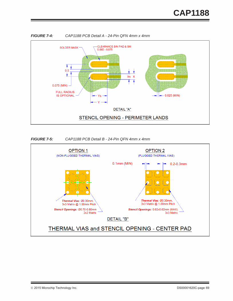
2015 Microchip Technology Inc. DS00001620C-page 69
CAP1188
FIGURE 7-4: CAP1188 PCB Detail A - 24-Pin QFN 4mm x 4mm
FIGURE 7-5: CAP1188 PCB Detail B - 24-Pin QFN 4mm x 4mm
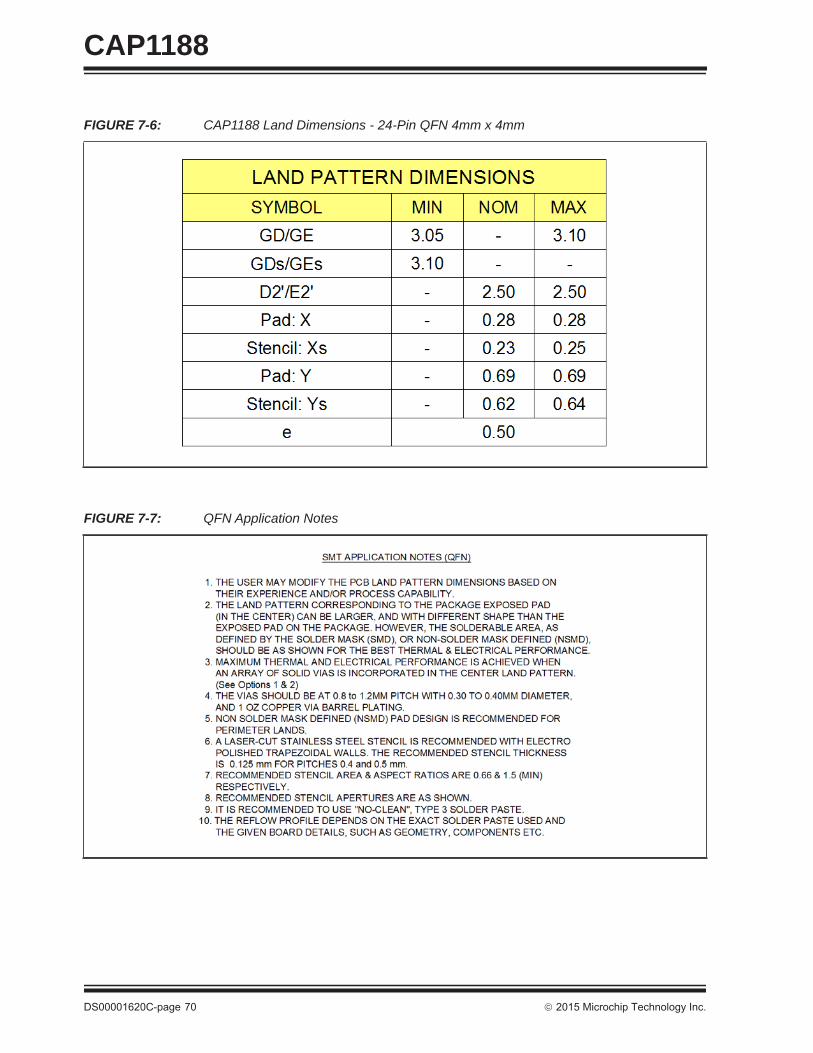
CAP1188
DS00001620C-page 70 2015 Microchip Technology Inc.
FIGURE 7-6: CAP1188 Land Dimensions - 24-Pin QFN 4mm x 4mm
FIGURE 7-7: QFN Application Notes
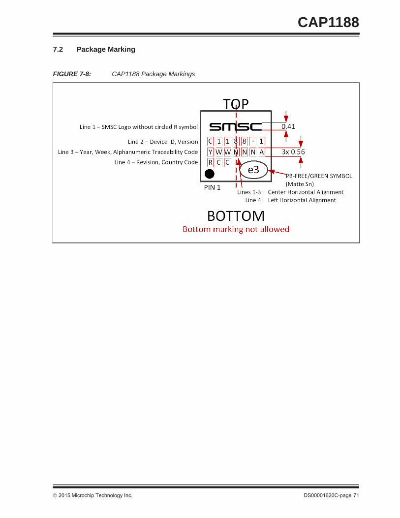
2015 Microchip Technology Inc. DS00001620C-page 71
CAP11887.2 Package Marking
FIGURE 7-8: CAP1188 Package Markings
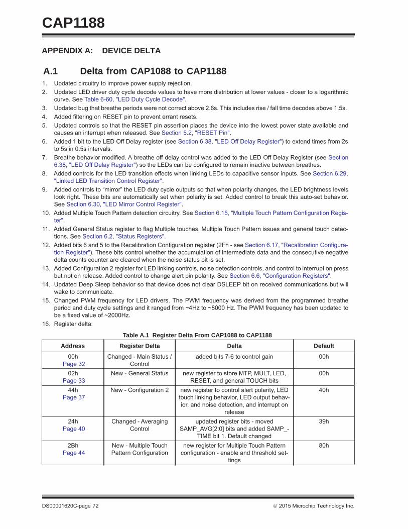
CAP1188
DS00001620C-page 72 2015 Microchip Technology Inc.
APPENDIX A: DEVICE DELTA
A.1 Delta from CAP1088 to CAP11881. Updated circuitry to improve power supply rejection. 2. Updated LED driver duty cycle decode values to have more distribution at lower values - closer to a logarithmic
curve. See Table 6-60, "LED Duty Cycle Decode".3. Updated bug that breathe periods were not correct above 2.6s. This includes rise / fall time decodes above 1.5s. 4. Added filtering on RESET pin to prevent errant resets.5. Updated controls so that the RESET pin assertion places the device into the lowest power state available and
causes an interrupt when released. See Section 5.2, "RESET Pin". 6. Added 1 bit to the LED Off Delay register (see Section 6.38, "LED Off Delay Register") to extend times from 2s
to 5s in 0.5s intervals. 7. Breathe behavior modified. A breathe off delay control was added to the LED Off Delay Register (see Section
6.38, "LED Off Delay Register") so the LEDs can be configured to remain inactive between breathes.8. Added controls for the LED transition effects when linking LEDs to capacitive sensor inputs. See Section 6.29,
"Linked LED Transition Control Register".9. Added controls to “mirror” the LED duty cycle outputs so that when polarity changes, the LED brightness levels
look right. These bits are automatically set when polarity is set. Added control to break this auto-set behavior.See Section 6.30, "LED Mirror Control Register".
10. Added Multiple Touch Pattern detection circuitry. See Section 6.15, "Multiple Touch Pattern Configuration Regis-ter".
11. Added General Status register to flag Multiple touches, Multiple Touch Pattern issues and general touch detec-tions. See Section 6.2, "Status Registers".
12. Added bits 6 and 5 to the Recalibration Configuration register (2Fh - see Section 6.17, "Recalibration Configura-tion Register"). These bits control whether the accumulation of intermediate data and the consecutive negativedelta counts counter are cleared when the noise status bit is set.
13. Added Configuration 2 register for LED linking controls, noise detection controls, and control to interrupt on pressbut not on release. Added control to change alert pin polarity. See Section 6.6, "Configuration Registers".
14. Updated Deep Sleep behavior so that device does not clear DSLEEP bit on received communications but willwake to communicate.
15. Changed PWM frequency for LED drivers. The PWM frequency was derived from the programmed breatheperiod and duty cycle settings and it ranged from ~4Hz to ~8000 Hz. The PWM frequency has been updated tobe a fixed value of ~2000Hz.
16. Register delta:
Table A.1 Register Delta From CAP1088 to CAP1188
Address Register Delta Delta Default
00h Page 32
Changed - Main Status / Control
added bits 7-6 to control gain 00h
02h Page 33
New - General Status new register to store MTP, MULT, LED, RESET, and general TOUCH bits
00h
44h Page 37
New - Configuration 2 new register to control alert polarity, LED touch linking behavior, LED output behav-ior, and noise detection, and interrupt on
release
40h
24h Page 40
Changed - Averaging Control
updated register bits - moved SAMP_AVG[2:0] bits and added SAMP_-
TIME bit 1. Default changed
39h
2Bh Page 44
New - Multiple Touch Pattern Configuration
new register for Multiple Touch Pattern configuration - enable and threshold set-
tings
80h
2015 Microchip Technology Inc. DS00001620C-page 73
CAP1188
2Dh Page 45
New - Multiple Touch Pattern Register
new register for Multiple Touch Pattern detection circuitry - pattern or number of
sensor inputs
FFh
2Fh Page 45
Changed - Recalibration Configuration
updated register - updated CAL_CFG bit decode to add a 128 averages setting and
removed highest time setting. Default changed. Added bit 6 NO_CLR_INTD and
bit 5 NO_CLR_NEG.
8Ah
38h Page 47
Changed - Sensor Input Noise Threshold
updated register bits - removed bits 7 - 3 and consolidated all controls into bits 1 - 0. These bits will set the noise threshold for
all channels. Default changed
01h
39h Removed - Noise Threshold Register 2
removed register n/a
41h Page 48
Changed - Standby Con-figuration
updated register bits - moved STBY_AVG[2:0] bits and added STBY_-
TIME bit 1. Default changed
39h
77h Page 54
New - Linked LED Tran-sition Control
new register to control transition effect when LED linked to sensor inputs
00h
79h Page 55
New - LED Mirror Control new register to control LED output mirror-ing for brightness control when polarity
changed
00h
90h Page 61
Changed - LED Pulse 1 Duty Cycle
changed bit decode to be more logarithmic F0h
91h Page 61
Changed - LED Pulse 2 Duty Cycle
changed bit decode to be more logarithmic F0h
92h Page 61
Changed - LED Breathe Duty Cycle
changed bit decode to be more logarithmic F0h
93h Page 61
Changed - LED Direct Duty Cycle
changed bit decode to be more logarithmic F0h
95h Added controls - LED Off Delay
Added bits 6-4 BR_OFF_DLY[2:0]Added bit 3 DIR_OFF_DLY[3]
00h
FDh Page 66
Changed - Product ID Changed bit decode for CAP1188 50h
Table A.1 Register Delta From CAP1088 to CAP1188 (continued)
Address Register Delta Delta Default
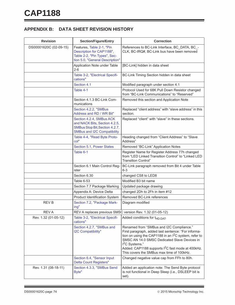
CAP1188
DS00001620C-page 74 2015 Microchip Technology Inc.
APPENDIX B: DATA SHEET REVISION HISTORY
Revision Section/Figure/Entry Correction
DS00001620C (02-09-15) Features, Table 2-1, "Pin Description for CAP1188", Table 2-2, "Pin Types", Sec-tion 5.0, "General Description"
References to BC-Link Interface, BC_DATA, BC_-CLK, BC-IRQ#, BC-Link bus have been removed
Application Note under Table 2-6
[BC-Link] hidden in data sheet
Table 3-2, "Electrical Specifi-cations"
BC-Link Timing Section hidden in data sheet
Section 4.1 Modified paragraph under section 4.1Table 4-1 Protocol Used for 68K Pull Down Resistor changed
from “BC-Link Communications” to “Reserved”Section 4.1.3 BC-Link Com-munications
Removed this section and Application Note
Section 4.2.2, "SMBus Address and RD / WR Bit"
Replaced “client address” with “slave address” in this section.
Section 4.2.4, SMBus ACK and NACK Bits, Section 4.2.5, SMBus Stop Bit,Section 4.2.7, SMBus and I2C Compatibility
Replaced “client” with “slave” in these sections.
Table 4-4, "Read Byte Proto-col"
Heading changed from “Client Address” to “Slave Address”
Section 5.1, Power States Removed “BC-Link” Application Notes Table 6-1 Register Name for Register Address 77h changed
from “LED Linked Transition Control” to “Linked LED Transition Control”
Section 6.1 Main Control Reg-ister
BC-Link paragraph removed from Bit 4 under Table 6-3
Section 6.30 changed CS8 to LED8Table 6-53 Modified B3 bit nameSection 7.7 Package Marking Updated package drawingAppendix A: Device Delta changed 2Dh to 2Fh in item #12Product Identification System Removed BC-Link references
REV B Section 7.2, "Package Mark-ing"
Diagram modified
REV A REV A replaces previous SMSC version Rev. 1.32 (01-05-12)Rev. 1.32 (01-05-12) Table 3-2, "Electrical Specifi-
cations"Added conditions for tHD:DAT.
Section 4.2.7, "SMBus and I2C Compatibility"
Renamed from “SMBus and I2C Compliance.” First paragraph, added last sentence: “For informa-tion on using the CAP1188 in an I2C system, refer to SMSC AN 14.0 SMSC Dedicated Slave Devices in I2C Systems.”Added: CAP1188 supports I2C fast mode at 400kHz. This covers the SMBus max time of 100kHz.
Section 6.4, "Sensor Input Delta Count Registers"
Changed negative value cap from FFh to 80h.
Rev. 1.31 (08-18-11) Section 4.3.3, "SMBus Send Byte"
Added an application note: The Send Byte protocol is not functional in Deep Sleep (i.e., DSLEEP bit is set).
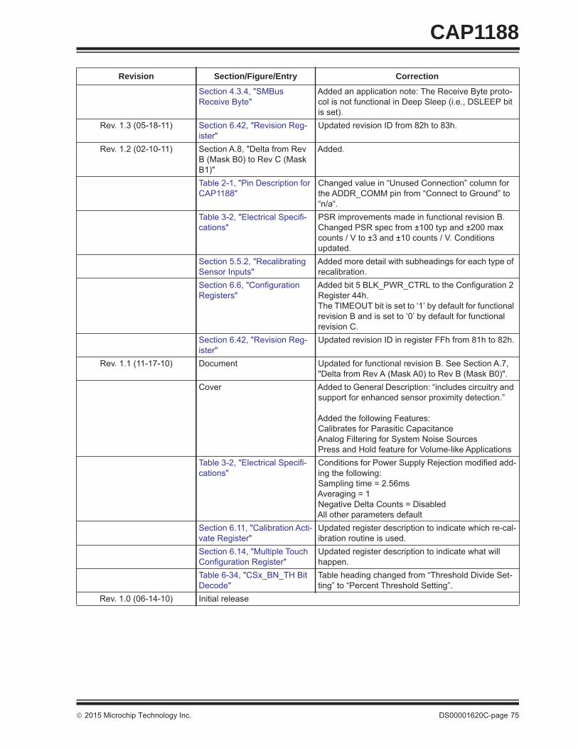
2015 Microchip Technology Inc. DS00001620C-page 75
CAP1188
Section 4.3.4, "SMBus Receive Byte"
Added an application note: The Receive Byte proto-col is not functional in Deep Sleep (i.e., DSLEEP bit is set).
Rev. 1.3 (05-18-11) Section 6.42, "Revision Reg-ister"
Updated revision ID from 82h to 83h.
Rev. 1.2 (02-10-11) Section A.8, "Delta from Rev B (Mask B0) to Rev C (Mask B1)"
Added.
Table 2-1, "Pin Description for CAP1188"
Changed value in “Unused Connection” column for the ADDR_COMM pin from “Connect to Ground” to “n/a“.
Table 3-2, "Electrical Specifi-cations"
PSR improvements made in functional revision B. Changed PSR spec from ±100 typ and ±200 max counts / V to ±3 and ±10 counts / V. Conditions updated.
Section 5.5.2, "Recalibrating Sensor Inputs"
Added more detail with subheadings for each type of recalibration.
Section 6.6, "Configuration Registers"
Added bit 5 BLK_PWR_CTRL to the Configuration 2 Register 44h.The TIMEOUT bit is set to ‘1’ by default for functional revision B and is set to ‘0’ by default for functional revision C.
Section 6.42, "Revision Reg-ister"
Updated revision ID in register FFh from 81h to 82h.
Rev. 1.1 (11-17-10) Document Updated for functional revision B. See Section A.7, "Delta from Rev A (Mask A0) to Rev B (Mask B0)".
Cover Added to General Description: “includes circuitry and support for enhanced sensor proximity detection.”
Added the following Features:Calibrates for Parasitic CapacitanceAnalog Filtering for System Noise SourcesPress and Hold feature for Volume-like Applications
Table 3-2, "Electrical Specifi-cations"
Conditions for Power Supply Rejection modified add-ing the following:Sampling time = 2.56msAveraging = 1Negative Delta Counts = DisabledAll other parameters default
Section 6.11, "Calibration Acti-vate Register"
Updated register description to indicate which re-cal-ibration routine is used.
Section 6.14, "Multiple Touch Configuration Register"
Updated register description to indicate what will happen.
Table 6-34, "CSx_BN_TH Bit Decode"
Table heading changed from “Threshold Divide Set-ting” to “Percent Threshold Setting”.
Rev. 1.0 (06-14-10) Initial release
Revision Section/Figure/Entry Correction
CAP1188
DS00001620C-page 76 2015 Microchip Technology Inc.
THE MICROCHIP WEB SITEMicrochip provides online support via our WWW site at www.microchip.com. This web site is used as a means to makefiles and information easily available to customers. Accessible by using your favorite Internet browser, the web site con-tains the following information:
• Product Support – Data sheets and errata, application notes and sample programs, design resources, user’s guides and hardware support documents, latest software releases and archived software
• General Technical Support – Frequently Asked Questions (FAQ), technical support requests, online discussion groups, Microchip consultant program member listing
• Business of Microchip – Product selector and ordering guides, latest Microchip press releases, listing of semi-nars and events, listings of Microchip sales offices, distributors and factory representatives
CUSTOMER CHANGE NOTIFICATION SERVICEMicrochip’s customer notification service helps keep customers current on Microchip products. Subscribers will receivee-mail notification whenever there are changes, updates, revisions or errata related to a specified product family ordevelopment tool of interest.
To register, access the Microchip web site at www.microchip.com. Under “Support”, click on “Customer Change Notifi-cation” and follow the registration instructions.
CUSTOMER SUPPORTUsers of Microchip products can receive assistance through several channels:
• Distributor or Representative• Local Sales Office• Field Application Engineer (FAE)• Technical Support
Customers should contact their distributor, representative or field application engineer (FAE) for support. Local salesoffices are also available to help customers. A listing of sales offices and locations is included in the back of this docu-ment.
Technical support is available through the web site at: http://www.microchip.com/support
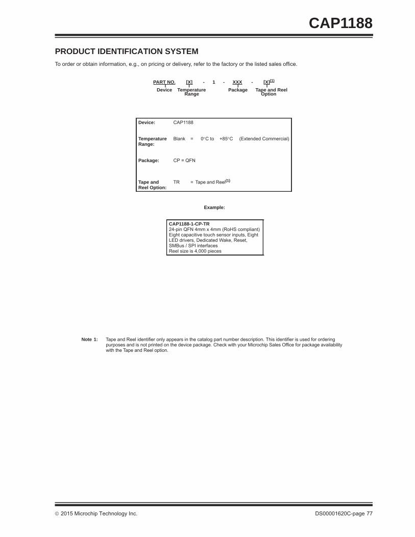
2015 Microchip Technology Inc. DS00001620C-page 77
CAP1188PRODUCT IDENTIFICATION SYSTEMTo order or obtain information, e.g., on pricing or delivery, refer to the factory or the listed sales office.
PART NO. [X] - 1 - XXX - [X](1) l l l l Device Temperature Package Tape and Reel Range Option
Example:
Note 1: Tape and Reel identifier only appears in the catalog part number description. This identifier is used for ordering purposes and is not printed on the device package. Check with your Microchip Sales Office for package availability with the Tape and Reel option.
Device: CAP1188
Temperature Range:
Blank = 0C to +85C (Extended Commercial)
Package: CP = QFN
Tape and Reel Option:
TR = Tape and Reel(1)
CAP1188-1-CP-TR24-pin QFN 4mm x 4mm (RoHS compliant)Eight capacitive touch sensor inputs, Eight LED drivers, Dedicated Wake, Reset, SMBus / SPI interfacesReel size is 4,000 pieces
CAP1188
DS00001620C-page 78 2015 Microchip Technology Inc.
Note the following details of the code protection feature on Microchip devices:• Microchip products meet the specification contained in their particular Microchip Data Sheet.
• Microchip believes that its family of products is one of the most secure families of its kind on the market today, when used in the intended manner and under normal conditions.
• There are dishonest and possibly illegal methods used to breach the code protection feature. All of these methods, to our knowledge, require using the Microchip products in a manner outside the operating specifications contained in Microchip’s Data Sheets. Most likely, the person doing so is engaged in theft of intellectual property.
• Microchip is willing to work with the customer who is concerned about the integrity of their code.
• Neither Microchip nor any other semiconductor manufacturer can guarantee the security of their code. Code protection does not mean that we are guaranteeing the product as “unbreakable.”
Code protection is constantly evolving. We at Microchip are committed to continuously improving the code protection features of ourproducts. Attempts to break Microchip’s code protection feature may be a violation of the Digital Millennium Copyright Act. If such actsallow unauthorized access to your software or other copyrighted work, you may have a right to sue for relief under that Act.
Information contained in this publication regarding device applications and the like is provided only for your convenience and may besuperseded by updates. It is your responsibility to ensure that your application meets with your specifications. MICROCHIP MAKES NOREPRESENTATIONS OR WARRANTIES OF ANY KIND WHETHER EXPRESS OR IMPLIED, WRITTEN OR ORAL, STATUTORY OROTHERWISE, RELATED TO THE INFORMATION, INCLUDING BUT NOT LIMITED TO ITS CONDITION, QUALITY, PERFORMANCE,MERCHANTABILITY OR FITNESS FOR PURPOSE. Microchip disclaims all liability arising from this information and its use. Use ofMicrochip devices in life support and/or safety applications is entirely at the buyer’s risk, and the buyer agrees to defend, indemnify andhold harmless Microchip from any and all damages, claims, suits, or expenses resulting from such use. No licenses are conveyed, implic-itly or otherwise, under any Microchip intellectual property rights.
Trademarks
The Microchip name and logo, the Microchip logo, dsPIC, FlashFlex, flexPWR, JukeBlox, KEELOQ, KEELOQ logo, Kleer, LANCheck, MediaLB, MOST, MOST logo, MPLAB, OptoLyzer, PIC, PICSTART, PIC32 logo, RightTouch, SpyNIC, SST, SST Logo, SuperFlash and UNI/O are registered trademarks of Microchip Technology Incorporated in the U.S.A. and other countries.
The Embedded Control Solutions Company and mTouch are registered trademarks of Microchip Technology Incorporated in the U.S.A.
Analog-for-the-Digital Age, BodyCom, chipKIT, chipKIT logo, CodeGuard, dsPICDEM, dsPICDEM.net, ECAN, In-Circuit Serial Programming, ICSP, Inter-Chip Connectivity, KleerNet, KleerNet logo, MiWi, MPASM, MPF, MPLAB Certified logo, MPLIB, MPLINK, MultiTRAK, NetDetach, Omniscient Code Generation, PICDEM, PICDEM.net, PICkit, PICtail, RightTouch logo, REAL ICE, SQI, Serial Quad I/O, Total Endurance, TSHARC, USBCheck, VariSense, ViewSpan, WiperLock, Wireless DNA, and ZENA are trademarks of Microchip Technology Incorporated in the U.S.A. and other countries.
SQTP is a service mark of Microchip Technology Incorporated in the U.S.A.
Silicon Storage Technology is a registered trademark of Microchip Technology Inc. in other countries.
GestIC is a registered trademarks of Microchip Technology Germany II GmbH & Co. KG, a subsidiary of Microchip Technology Inc., in other countries.
All other trademarks mentioned herein are property of their respective companies.
© 2015, Microchip Technology Incorporated, Printed in the U.S.A., All Rights Reserved.
ISBN: 9781632770301
Microchip received ISO/TS-16949:2009 certification for its worldwide headquarters, design and wafer fabrication facilities in Chandler and Tempe, Arizona; Gresham, Oregon and design centers in California and India. The Company’s quality system processes and procedures are for its PIC® MCUs and dsPIC® DSCs, KEELOQ® code hopping devices, Serial EEPROMs, microperipherals, nonvolatile memory and analog products. In addition, Microchip’s quality system for the design and manufacture of development systems is ISO 9001:2000 certified.

2015 Microchip Technology Inc. DS00001620C-page 79
AMERICASCorporate Office2355 West Chandler Blvd.Chandler, AZ 85224-6199Tel: 480-792-7200 Fax: 480-792-7277Technical Support: http://www.microchip.com/supportWeb Address: www.microchip.comAtlantaDuluth, GA Tel: 678-957-9614 Fax: 678-957-1455Austin, TXTel: 512-257-3370 BostonWestborough, MA Tel: 774-760-0087 Fax: 774-760-0088ChicagoItasca, IL Tel: 630-285-0071 Fax: 630-285-0075ClevelandIndependence, OH Tel: 216-447-0464 Fax: 216-447-0643DallasAddison, TX Tel: 972-818-7423 Fax: 972-818-2924DetroitNovi, MI Tel: 248-848-4000Houston, TX Tel: 281-894-5983IndianapolisNoblesville, IN Tel: 317-773-8323Fax: 317-773-5453Los AngelesMission Viejo, CA Tel: 949-462-9523 Fax: 949-462-9608New York, NY Tel: 631-435-6000San Jose, CA Tel: 408-735-9110Canada - TorontoTel: 905-673-0699 Fax: 905-673-6509
ASIA/PACIFICAsia Pacific OfficeSuites 3707-14, 37th FloorTower 6, The GatewayHarbour City, KowloonHong KongTel: 852-2943-5100Fax: 852-2401-3431Australia - SydneyTel: 61-2-9868-6733Fax: 61-2-9868-6755China - BeijingTel: 86-10-8569-7000 Fax: 86-10-8528-2104China - ChengduTel: 86-28-8665-5511Fax: 86-28-8665-7889China - ChongqingTel: 86-23-8980-9588Fax: 86-23-8980-9500China - DongguanTel: 86-769-8702-9880 China - HangzhouTel: 86-571-8792-8115 Fax: 86-571-8792-8116China - Hong Kong SARTel: 852-2943-5100 Fax: 852-2401-3431China - NanjingTel: 86-25-8473-2460Fax: 86-25-8473-2470China - QingdaoTel: 86-532-8502-7355Fax: 86-532-8502-7205China - ShanghaiTel: 86-21-5407-5533 Fax: 86-21-5407-5066China - ShenyangTel: 86-24-2334-2829Fax: 86-24-2334-2393China - ShenzhenTel: 86-755-8864-2200 Fax: 86-755-8203-1760China - WuhanTel: 86-27-5980-5300Fax: 86-27-5980-5118China - XianTel: 86-29-8833-7252Fax: 86-29-8833-7256
ASIA/PACIFICChina - XiamenTel: 86-592-2388138 Fax: 86-592-2388130China - ZhuhaiTel: 86-756-3210040 Fax: 86-756-3210049India - BangaloreTel: 91-80-3090-4444 Fax: 91-80-3090-4123India - New DelhiTel: 91-11-4160-8631Fax: 91-11-4160-8632India - PuneTel: 91-20-3019-1500Japan - OsakaTel: 81-6-6152-7160 Fax: 81-6-6152-9310Japan - TokyoTel: 81-3-6880- 3770 Fax: 81-3-6880-3771Korea - DaeguTel: 82-53-744-4301Fax: 82-53-744-4302Korea - SeoulTel: 82-2-554-7200Fax: 82-2-558-5932 or 82-2-558-5934Malaysia - Kuala LumpurTel: 60-3-6201-9857Fax: 60-3-6201-9859Malaysia - PenangTel: 60-4-227-8870Fax: 60-4-227-4068Philippines - ManilaTel: 63-2-634-9065Fax: 63-2-634-9069SingaporeTel: 65-6334-8870Fax: 65-6334-8850Taiwan - Hsin ChuTel: 886-3-5778-366Fax: 886-3-5770-955Taiwan - KaohsiungTel: 886-7-213-7828Taiwan - TaipeiTel: 886-2-2508-8600 Fax: 886-2-2508-0102Thailand - BangkokTel: 66-2-694-1351Fax: 66-2-694-1350
EUROPEAustria - WelsTel: 43-7242-2244-39Fax: 43-7242-2244-393Denmark - CopenhagenTel: 45-4450-2828 Fax: 45-4485-2829France - ParisTel: 33-1-69-53-63-20 Fax: 33-1-69-30-90-79Germany - DusseldorfTel: 49-2129-3766400Germany - MunichTel: 49-89-627-144-0 Fax: 49-89-627-144-44Germany - PforzheimTel: 49-7231-424750Italy - Milan Tel: 39-0331-742611 Fax: 39-0331-466781Italy - VeniceTel: 39-049-7625286 Netherlands - DrunenTel: 31-416-690399 Fax: 31-416-690340Poland - WarsawTel: 48-22-3325737 Spain - MadridTel: 34-91-708-08-90Fax: 34-91-708-08-91Sweden - StockholmTel: 46-8-5090-4654UK - WokinghamTel: 44-118-921-5800Fax: 44-118-921-5820
Worldwide Sales and Service
01/27/15