California PC FLASH CompactFlash™ Card Full...
68
CaliforniaPC.com California Peripherals & Components, Inc. “WorldWide Supplier of Computer Hardware & Software” Any Where. AnyTemperature.* California PC FLASH CompactFlash™ Card Full Specifications Series II Industrial Grade -40°C to +85°C California Peripherals & Components, Inc. www.CaliforniaPC.com California_PC_FLASH_CF_specs_full-V-02.3 California PC FLASH - Industrial Grade CompactFlash California PC FLASH - CompactFlash (CF) Full Specifications - 32MB to 16GB V02.3 1
Transcript of California PC FLASH CompactFlash™ Card Full...

CaliforniaPC.com California Peripherals & Components, Inc.
“WorldWide Supplier of Computer Hardware & Software”
Any Where. AnyTemperature.*
California PC FLASH CompactFlash™ Card Full
Specifications Series II
Industrial Grade -40°C to +85°C
California Peripherals & Components, Inc.
www.CaliforniaPC.com
California_PC_FLASH_CF_specs_full-V-02.3
California PC FLASH - Industrial Grade CompactFlash
California PC FLASH - CompactFlash (CF) Full Specifications - 32MB to 16GB V02.3 1

Contents: 1. Scope.................................................................................................................. 2
2. Introduction ....................................................................................................... 2
3. System Features................................................................................................ 3
4. Product Specifications...................................................................................... 4
4.1. System Environmental Specification .................................................... 4
4.2. System Power Requirement .................................................................. 4
4.3. System Performance .............................................................................. 5
4.4. System Reliability ................................................................................... 5
4.5. Physical Specifications .......................................................................... 6
4.5.1. Physical Specifications ....................................................................... 6
4.5.2. Dimension ............................................................................................... 6
4.6. Capacity Specification............................................................................ 7
4.7. Card Block Diagram ............................................................................... 7
5. Interface Description......................................................................................... 8
5.1. Pin Assignments ..................................................................................... 8
5.2. Pin Descriptions ................................................................................... 10
6. Electrical Specification ................................................................................... 16
6.1. Power Pin Description.......................................................................... 16
6.2. Absolute Maximum Rating................................................................... 16
6.2.1. CompactFlash interface I/O at 5.0V ................................................ 16
6.2.2. CompactFlash interface I/O at 3.3V ................................................ 17
6.2.3. The I/O pins other than CompactFlash interface........................ 18
6.3. Recommended Operating Conditions ................................................ 18
6.4. AC Characteristics................................................................................ 19
6.4.1. Attribute Memory Read Timing........................................................ 19
6.4.2. Configuration Register (Attribute Memory) Write Timing ........ 20
6.4.3. Common Memory Read Timing ....................................................... 21
6.4.4. Common Memory Write Timing....................................................... 22
6.4.5. I/O Read Timing ................................................................................... 24
6.4.6. I/O Write Timing ................................................................................... 26
6.4.7. True IDE PIO Mode Read/Write Timing.......................................... 28
6.4.8. True IDE Multiword DMA Mode Read/Write Timing ................... 31
6.4.9. Ultra DMA Signal Usage In Each Interface Mode........................ 33
6.4.10. Ultra DMA Data Burst Timing Requirements ............................... 30
6.4.11. Ultra DMA Data Burst Timing Descriptions.................................. 32
6.4.12. Ultra DMA Sender and Recipient IC Timing Requirements ..... 34
California PC FLASH - Industrial Grade CompactFlash
California PC FLASH - CompactFlash (CF) Full Specifications - 32MB to 16GB V02.3 2

6.4.13. Ultra DMA AC Signal Requirements............................................... 35
6.4.14. Ultra DMA Data-In Burst Initiation Timing .................................... 36
6.4.15. Sustained Ultra DMA Data-In Burst Timing .................................. 37
6.4.16. Ultra DMA Data-In Burst Host Pause Timing ............................... 38
6.4.17. Ultra DMA Data-In Burst Device Termination Timing ................ 39
6.4.18. Ultra DMA Data-In Burst Host Termination Timing .................... 40
6.4.19. Ultra DMA Data-Out Burst Initiation Timing ................................. 41
6.4.20. Sustained Ultra DMA Data-Out Burst Timing............................... 42
6.4.21. Ultra DMA Data-Out Burst Device Pause Timing ........................ 43
6.4.22. Ultra DMA Data-Out Burst Device Termination Timing............. 44
6.4.23. Ultra DMA Data-Out Burst Host Termination Timing................. 45
7. CF – ATA Command Description .................................................................... 46
7.1. CF – ATA Command Set ....................................................................... 47
7.2. SMART Command Support.................................................................. 48
7.3. Identify Drive Information(True IDE Mode) ......................................... 50
7.4. ID Table Information (PCMCIA Mode).................................................. 52
APPENDIX ............................................................................................................... 61
A. Order Information..................................................................................... 61
1. Part Number .......................................................................................... 61
2. Part Number Decoder ........................................................................... 61
California PC FLASH - Industrial Grade CompactFlash
California PC FLASH - CompactFlash (CF) Full Specifications - 32MB to 16GB V02.3 3

1. Scope
2. Introduction
This document describes the features and specifications and installation guide of California PC FLASH CompactFlashTM Cards. In the appendix there is order
information with all part numbers and standard options.
The California PC FLASH CompactFlashTM Cards are designed based on
CompactFlashTM Card Specification 3.0 with a flash memory controller and NAND-Type
flash memory. It can support a capacity of 16MB, 32MB, 64MB,128MB, 256MB, 512MB,
1GB, 2GB, 4GB, 8GB, and 16GB. The California PC FLASH CompactFlashTM card is available with Commercial operating temperature grade (0℃~+70 ℃) and Industrial operating temperature grade (-40ÜC ~ +85ºC) to work with various specialized applications in normal or harsh operating environments. CompactFlashTM Card is
ideal solution for critical applications which request for long term supply with consistent
key components.
California PC FLASH - Industrial Grade CompactFlash
California PC FLASH - CompactFlash (CF) Full Specifications - 32MB to 16GB V02.3 4

3. System Features
CompactFlashTM Card Specification 3.0 compliant
Operating Modes:
PC Card Memory Mode.
PC Card I/O Mode.
True-IDE Mode.
Ultra DMA Mode supported up to Mode 4
Hardware RS-code ECC capable of correcting 24 bits in a 1,024 byte data
Reliable wear-leveling algorithm to ensure the best of flash endurance.
Very low power consumption
Very high performance
Rugged environment is working well
Automatic error correction and retry capabilities
Supports power down commands and Auto Stand-by / Sleep Mode
+5 V ±10% or +3.3 V ±5% operation
Low weight
Noiseless
MTBF > 1,000,000 hours
Minimum 10,000 insertions
Support O/S: Windows 31/95/98/Me, Windows NT/2000/XP/2003, WinCE, QNX,
Linux, DOS and more
Capacity:128MB, 256MB, 512 MB, 1GB, 2GB, 4GB, 8GB, 16GB,
32GB(unformatted)
California PC FLASH - Industrial Grade CompactFlash
California PC FLASH - CompactFlash (CF) Full Specifications - 32MB to 16GB V02.3 5

4. Product Specifications
For all the following specifications, values are defined at ambient temperature and nominal supply voltage unless otherwise stated.
4.1. System Environmental Specifications Reference Part Number FCFX1-XXXX2-X3X4XX
Commercial Temperature
Operating 0°C to +70ºC Non-operating -20°C to +80ºC
Industrial Temperature
Operating -40°C to +70ºC Non-operating -50° to +95º
Humidity Operating 5% ~ 95% non-condensing Non-operating
Vibration Operating 15G peak-to-peak maximum Non-operating
Shock Operating 2,000 G maximum Non-operating
Altitude Operating 50,000 fee maximum Non-operatingPart Number Notes:
1) X1: Blank = Commercial Temperature (0°C to 70°C) and I = IndustrialTemperature (-40° to +85°)
2) XXXX2: Capacities include 16MB, 32MB, 64MB, 128MB, 256MB, 512MB,01GB, 02GB, 04GB, 08GB, and 16GB
3) X3: Transfer mode: 2 = (PIO 4), 3 = DMA 2 (Multi Word), 4 = UDMA 4 (UltraDMA 4)
4) X4: Disk mode: 1 = Removable Disk Mode, 2 = Fixed Disk Mode, 3 = AutoDetect Disk Mode
California PC FLASH - Industrial Grade CompactFlash
California PC FLASH - CompactFlash (CF) Full Specifications - 32MB to 16GB V02.3 6

4.3. System Performance
Data Transfer Rate To/From Flash 25 Mbytes /sec burst
Ultra DMA mode 4 66 Mbytes /sec burst Data Transfer Rate To/From Host PIO mode 4 16.6Mbytes /sec burst
Sequential Read 43 M bytes / sec Max. SLC Performance
Sequential Write 35 M bytes / sec Max.
Sequential Read 35 M bytes / sec Max. MLC Performance
Sequential Write 15.5 M bytes / sec Max.
4.4. System Reliability
MTBF > 1,000,000 hours
Data Reliability < 1 non-recoverable error in 1014 bits read < 1 erroneous correction in 1020 bits read
Wear-leveling Algorithms Supportive
ECC Technology Hardware RS-code ECC capable of correcting 24 bits in a 1,024 byte data
Endurance (SLC) Greater than 1,000,000 cycles Logically contributed by Wear-leveling and advanced bad sector management
Endurance (MLC) Greater than 100,000 cycles Logically contributed by Wear-leveling and advanced bad sector management
Data Retention 10 years
California PC FLASH - Industrial Grade CompactFlash
California PC FLASH - CompactFlash (CF) Full Specifications - 32MB to 16GB V02.3 7

4.5. Physical Specifications
4.5.1. Physical Specifications
Length 36.40 ± 0.15 mm (1.433 ±.006 in)
Width 42.80 ± 0.10 mm (1.685 ±.004 in)
Thickness 3.3 mm ± 0.10 mm (.130 ±.004 in) (Excluding Lip)
Weight 11.4 g (.40 oz) typical, 14.2 g (.50 oz) maximum
4.5.2. Dimension
California PC FLASH - Industrial Grade CompactFlash
California PC FLASH - CompactFlash (CF) Full Specifications - 32MB to 16GB V02.3 8

4.6. Capacity Specification
The specific capacities for the various models and the default number of heads,
sectors and cylinders.
Capacity Default Cylinder Default Head Default Sector User Data Size
128MB 253 16 63
256MB 500 16 63
512MB 991 16 63
1GB 1,966 16 63
2GB 3,900 16 63
4GB 7,785 16 63
8GB 15,538 16 63
16GB 31,045 16 63
32GB 62,041 16 63
Depended on file
management
4.7. Card Block Diagram
California PC FLASH - Industrial Grade CompactFlash
California PC FLASH - CompactFlash (CF) Full Specifications - 32MB to 16GB V02.3 9

5. Interface Description
5.1. Pin Assignments
Memory card mode I/O card mode True IDE mode
Pin NO. Signal name I/O Signal name I/O Signal name I/O
1 GND - GND - GND -
2 D3 I/O D3 I/O D3 I/O
3 D4 I/O D4 I/O D4 I/O
4 D5 I/O D5 I/O D5 I/O
5 D6 I/O D6 I/O D6 I/O
6 D7 I/O D7 I/O D7 I/O
7 -CE1 I -CE1 I -CE0 I
8 A10 I A10 I A102 I
9 -OE I -OE I -ATA SEL I
10 A9 I A9 I A92 I
11 A8 I A8 I A82 I
12 A7 I A7 I A72 I
13 VCC - VCC - VCC -
14 A6 I A6 I A62 I
15 A5 I A5 I A52 I
16 A4 I A4 I A42 I
17 A3 I A3 I A32 I
18 A2 I A2 I A2 I
19 A1 I A1 I A1 I
20 A0 I A0 I A0 I
21 D0 I/O D0 I/O D0 I/O
22 D1 I/O D1 I/O D1 I/O
23 D2 I/O D2 I/O D2 I/O
24 WP O -IOIS16 O -IOCS16 O
25 -CD2 O -CD2 O -CD2 O
26 -CD1 O -CD1 O -CD1 O
27 D111 I/O D111 I/O D111 I/O
28 D121 I/O D121 I/O D121 I/O
29 D131 I/O D131 I/O D131 I/O
California PC FLASH - Industrial Grade CompactFlash
California PC FLASH - CompactFlash (CF) Full Specifications - 32MB to 16GB V02.3 10

Memory card mode I/O card mode True IDE mode
Pin NO. Signal name I/O Signal name I/O Signal name I/O
30 D141 I/O D141 I/O D141 I/O
31 D151 I/O D151 I/O D151 I/O
32 -CE21 I -CE21 I -CE11 I
33 -VS1 O -VS1 O -VS1 O
-IORD7
HSTROBE834 -IORD I -IORD I
-HDMARDY9
I
-IOWR7
35 -IOWR I -IOWR ISTOP8, 9
I
36 -WE I -WE I -WE3 I
37 RDY/-BSY O -IREQ O INTRQ O
38 VCC — VCC — VCC —
39 -CSEL5 I -CSEL5 I -CSEL I
40 -VS2 O -VS2 O -VS2 O
41 RESET I RESET I -RESET I
-IORDY7
-DDMARDY8 42 -WAIT O -WAIT O
DSTROBE9
O
43 -INPACK O -INPACK O DMARQ O
44 -REG I -REG I -DMACK6 I
45 BVD2 I/O -SPKR I/O -DASP I/O
46 BVD1 I/O -STSCHG I/O -PDIAG I/O
47 D81 I/O D81 I/O D81 I/O
48 D91 I/O D91 I/O D91 I/O
49 D101 I/O D101 I/O D101 I/O
50 GND — GND — GND —
Note:
1) These signals are required only for 16 bit accesses and not required when installed in 8 bit
systems. Devices should allow for 3-state signals not to consume current.
2) The signal should be grounded by the host.
3) The signal should be tied to VCC by the host.
4) The mode is optional for CF+ Cards, but required for CompactFlashTM Storage Cards.
California PC FLASH - Industrial Grade CompactFlash
California PC FLASH - CompactFlash (CF) Full Specifications - 32MB to 16GB V02.3 11

5) The -CSEL signal is ignored by the card in PC Card modes. However, because it is not pulled
up on the card in these modes, it should not be left floating by the host in PC Card modes. In
these modes, the pin should be connected by the host to PC Card A25 or grounded by the host.
6) If DMA operations are not used, the signal should be held high or tied to VCC by the host. For
proper operation in older hosts: while DMA operations are not active, the card shall ignore this
signal, including a floating condition
7) Signal usage in True IDE Mode except when Ultra DMA mode protocol is active.
8) Signal usage in True IDE Mode when Ultra DMA mode protocol DMA Write is active.
9) Signal usage in True IDE Mode when Ultra DMA mode protocol DMA Read is active.
5.2. Pin Descriptions
Signal Name Dir Pin No. Description
A10 to A0
(PC Card Memory
Mode)
A10 to A0
(PC Card I/O Mode)
8,10,11,12,14,15,
16,17,18,19,20
These address lines along with the-REG
signal are used to select the following: The
I/O port address registers within the
CompactFlashTM Storage Card or CF + Card,
the memory mapped port add address
registers within the CompactFlashTM Storage
Card or CF+ Card , a byte in the card’s
information structure and its configuration
control and status registers.
A2 to A0
(True IDE Mode)
I
18,19,20
In True IDE Mode only {2:0} are used to
select the one of eight registers in the Task
File. The remaining address lines should be
grounded by the host.
BVD1
(PC Card Memory
mode)
This signal is asserted high as BVD1 is not
supported.
-STSCHG
(PC Card Memory
Mode)
This Signal is asserted low to alert the host
to changes in the RDY/-BSY and Write
Protect states; while the I/O interface is
configured. Its use is controlled by the Card
Configured and Status Register.
-PDIAG
(True IDE Mode)
I/O 46
In the True IDE Mode, this input/output is the
Pass Diagnostic signal in the Master/Slave
handshake protocol.
California PC FLASH - Industrial Grade CompactFlash
California PC FLASH - CompactFlash (CF) Full Specifications - 32MB to 16GB V02.3 12

Signal Name Dir Pin No. Description
BVD2 (PC Card Memory
Mode)
This signal is asserted high, as BVD2 is not supported.
-SPKR (PC Card I/O Mode)
This line is Binary AUDIO OUTPUT From the Card. If the Card doesn’t support the Binary Audio function, this line should be held
negated.
-DASP (True IDE Mode)
I/O 45
In the True IDE Mode, this input/output is the Disk Active/Slave Present signal in the Master/Slave.
-CD1, -CD2
(PC Card Memory Mode)
O 25,26
These Card Detect pins are connected to
ground on the CompactFlashTM Storage Card or CF+ Card. They are used by the host to determined that the CompactFlashTM
Storage Card or CF+ Card is fully inserted into its socket.
-CE1,-CE2 (PC Card Memory
Mode)
-CE1,-CE2 (PC Card I/O Mode)
There input signals are used both to select the card and to indicate to the card whether
a byte or a word operation is being performed. –CE2 always accesses the odd byte of the word depending on A0 and –CE2.
A multiplexing scheme based on A1. –DE1, -CE2 allow 8-bit hosts to access all data on D0 to D7. See Access Specification below.
-CS0,-CS1
(True IDE Mode)
I 7,32
In the True IDE Mode CS0 is the chip select
for the task file registers while CS1 is used to select the Alternate Status Register and Device Control Register.
-CSEL
(PC Card Memory Mode)
This signal is not used for this mode.
-CSEL (PC Card I/O Mode)
-CSEL
(True IDE Mode)
I 39This internally pulled up signal is used to configure this device as a Master or a Slave
when configured in the True IDE Mode. When this pin is grounded, this device is configured as a Master. When the pin is
open, this device is configured as a Slave.
D15 to D00 (PC Card Memory
Mode)
D15 to D00
(PC Card I/O Mode)
I/O 31,30,29,38,37,49,48,48,6,5,4,3,2,2
3,22,21
These lines carry the Data, commands and Status information between the host and the controller. D00 is the LSB of the Even Byte
of the Word D08 is the LSB of the Odd Byte of the Word.
California PC FLASH - Industrial Grade CompactFlash
California PC FLASH - CompactFlash (CF) Full Specifications - 32MB to 16GB V02.3 13

Signal Name Dir Pin No. Description
D15 to D00 (True IDE Mode)
I/O
31,30,29,38,37,49,48,48,6,5,4,3,2,2
3,22,21
True IDE Mode, all Task File operations occur in byte mode on the low order bus D00
to D07 while all data transfers are 16 but using D00 to D15.
GND (PC Card Memory
Mode)
GND (PC Card I/O Mode)
GND (True IDE Mode)
Ground
-INPCAK
(PC Card Memory Mode)
This signal is not used in this Mode.
-INPACK (PC Card I/O Mode)
The Input Acknowledge signal is asserted by the CompactFlashTM Storage Card or CF+
Card when the card is selected and responding to an I/O read cycle at the address that is on the address bus. This
signal is used by the host to control the enable of any input data buffers between the CompactFlashTM Storage Card or CF+ Card
and the CPU.
-INPACK (True IDE Mode)
O 43
In True IDE Mode this output signal is not used and should not be connected at the host.
-IORD
(PC Card Memory Mode)
This signal is not used in this mode.
-IORD (PC Card I/O Mode)
This is an I/O Read strobe generated by the host. This signal gates I/O data onto the bus
from the CompactFlashTM Storage Card or CF+ Card when the card is configured to use the I/O interface.
-IORD
(True IDE Mode)
I 34
In True IDE Mode, this signal has same
function as in PC Card I/O Mode.
California PC FLASH - Industrial Grade CompactFlash
California PC FLASH - CompactFlash (CF) Full Specifications - 32MB to 16GB V02.3 14

Signal Name Dir Pin No. Description
-IOWR (PC Card Memory
Mode)
This signal is not used in this mode.
-IOWR (PC Card I/O Mode)
The I/O Write strobe pulse is used to clock I/O data on the Card Data bus into the CompactFlashTM Storage Card or CF+ Card
controller registers when he Compact Storage Card or CF+ Card is configured to use the I/O interface. The clocking will occur
on the negative to positive edge of the signal (Trailing edge).
-IOWR (True IDE Mode)
I 35
In True IDE Mode, this signal has the same function as in PC Card I/O Mode.
-OE
(PC Card Memory Mode)
This is an Output Enable strobe generated
by the host interface. It is used to read data from the CompactFlashTM Storage Card or CF+ Card in Memory Mode and to read the
CIS and configuration registers.
-OE (PC Card I/O Mode)
In PC Card I/O Mode. This signal is used to read the CIS and configuration registers.
-ATA SEL (True IDE Mode)
I 9
To enable True IDE Mode this input should be grounded by the host.
PDY/BSY
(PC Card Memory Mode)
O 37
In Memory Mode this signal is set high when
the CompactFlashTM Storage Card or CF+ Card is ready to accept a new data transfer operation and held low when the card is
busy. Theo Host memory card socket must provide a pull-up resistor. At power up and at Reset the RDY/-BSY signal is held low
(busy) until the CompactFlashTM Storage Card or CF+ Card has completed its power up or reset function. No access of any type
should be made to the CompactFlashTM Storage Card or CF+ Card during this time. The RDY/-BSY signal is held high (disabled
from being busy) whenever the following condition is true. The CompactFlashTM Storage Card or CF+ Card has been
powered up with + RESET continuously disconnected or asserted.
California PC FLASH - Industrial Grade CompactFlash
California PC FLASH - CompactFlash (CF) Full Specifications - 32MB to 16GB V02.3 15

Signal Name Dir Pin No. Description
-IREQ (PC Card I/O Mode)
Operation – After the CompactFlashTM Storage Card or CF+ Card has been
configured for I/O operational this signal is used as interrupt Request. This line is strobe low to generate a pulse mode interrupt or
held low for a level mode interrupt.
INTRO (True IDE Mode)
In True IDE Mode signal is the active high interrupt Request to the host.
-REG (PC Card Memory
Mode)
This signal is used during Memory Cycles to distinguish between Common Memory and
Register (Attribute) Memory accesses. High for Common Memory. Low for Attribute Memory.
-REG
(PC Card I/O Mode)
The signal must also be active (low) during
I/O Cycles when the I/O address is on the Bus.
-REG (True IDE Mode)
I 44
In the True IDE Mode this input pin is the active low hardware reset from the host.
RESET
(PC Card Memory Mode)
RESET (PC Card I/O Mode)
When the pin is high, this signal Resets the
CompactFlashTM Storage Card or CF+ Card. The CompactFlashTM Card or CF+ Car is Reset only at power up if this pin is left high
or open from power-up. The CompactFlashTM Storage CF Card or CF+ Card is also Reset when the Soft Reset bit in
the Card Configuration Option Register is set.
RESET (True IDE Mode)
I 41
In the True IDE Mode this input pin is the active low hardware reset from the host.
VCC
(PC Card Memory Mode)
(PC Card I/O Mode)
(True IDE Mode)
- 13,38
+5V, +3.3V power
-VS1/-VS2 (PC Card Memory
Mode)
(PC Card I/O Mode) (True IDE Mode)
O 3,40
Voltage Sense Signals. – VS1 is grounded o that the CompactFlashTM Storage Card or CF+ Card CIS can be read at 3.3 volts
and –VS2 is reserved by PCMCIA for a secondary voltage.
California PC FLASH - Industrial Grade CompactFlash
California PC FLASH - CompactFlash (CF) Full Specifications - 32MB to 16GB V02.3 16

Signal Name Dir Pin No. Description
-WAIT (PC Card Memory
Mode)
The –Wait signal is driven low by the CompactFlashTM Storage Card or CF+ Card
to signal the host to delay completion of a memory or I/O cycles that is in progress.
IORDY (True IDE Mode)
O 42
In True IDE Mode this output signal may be used as IORDY.
-WE
(PC Card Memory Mode)
This is a signal driven by the host and used
for starting memory write data to the registers of the CompactFlashTM Storage Card or CF+ Card when the card is
configured I the memory interface mode. It is also used for writing the configuration registers.
-WE
(PC Card I/O Mode)
In PC Card I/O Mode, this signal is used for
writing the configuration registers.
-WE (True IDE Mode)
I 36
In True IDE Mode this input signal is not used and should be connected to VCC by the Host.
WP
(PC Card Memory Mode)
O 24
Memory Mode-The CompactFlashTM
Storage Card or CF+ Card does not have a write protect switch. This signal is held low after the completion of the reset initialization
sequence.
-IOIS16 (PC Card I/O Mode)
I/O Operation-When the CompactFlashTM Storage Card or CF+ Card is configured for I/O operation Pin 24 is used for the – I/O
Selected is 16 Bit Port (-IOIS1) function. A Low signal indicates that a 16 bit or odd byte only operation can be performed at the
addressed port.
-IOIS16 (True IDE Mode)
In True IDE Mode this output signal is asserted low when this device is expecting a word data transfer cycle.
California PC FLASH - Industrial Grade CompactFlash
California PC FLASH - CompactFlash (CF) Full Specifications - 32MB to 16GB V02.3 17
6. Electrical Specification
Commercial Temperature Products
VCC = 5V ±10% VCC = 3.3V ± 5% Ta = 0°C to 70°C
6.1. Power Pin Description
Pin Name I/O Description
VCCk Power Host VCC
VCC 3.3V Power 3.3V VCC
GND Power GND
6.2. Absolute Maximum Rating
6.2.1. CompactFlash interface I/O at 5.0V
Symbol Parameter Min. Max. Units
VCC Power Supply 4.5 5.5 V
VOH Output Voltage High Level VCC-0.8 V
VOL Output Voltage Low Level 0.8 V
VIH Input Voltage High Level 2.92 V
VIL Input Voltage Low Level 1.7 V
TOPR-W Operating temperature for wide grade -40 +85 ℃
TOPR-S Operating temperature for standard grade 0 +70 ℃
TSTG Storage temperature -40 125 ℃
The following table defines all D.C. Characteristics for the CompactFlashTM Series. The conditions are:
California PC FLASH - Industrial Grade CompactFlash
California PC FLASH - CompactFlash (CF) Full Specifications - 32MB to 16GB V02.3 18

6.2.2. CompactFlash interface I/O at 3.3V
Symbol Parameter Min. Max. Units
VCC Power Supply 2.97 3.63 V
VOH Output Voltage High Level VCC-0.8 V
VOL Output Voltage Low Level 0.8 V
VIH Input Voltage High Level 2.05 V
VIL Input Voltage Low Level 1.25 V
TOPR-W Operating Temperature For Wide Grade -40 +85 ℃
TOPR-S Operating Temperature For Standard Grade 0 +70 ℃
TSTG Storage Temperature -40 125 ℃
California PC FLASH - Industrial Grade CompactFlash
California PC FLASH - CompactFlash (CF) Full Specifications - 32MB to 16GB V02.3 19

6.2.3. The I/O pins other than CompactFlash interface
Symbol Parameter Min. Max. Unit Remark
VCC Supply Voltage 2.7 3.6 V
VOH High level output voltage 2.4 V
VOL Low level output voltage 0.4 V
2.0 V Non-Schmitt triggerVIH High level input voltage
1.4 2.0 V Schmitt trigger3
0.8 V Non-Schmitt triggerVIL Low level input voltage
0.8 1.2 V Schmitt trigger3
6.3. Recommended Operating Conditions
Symbol Parameter Min Typ Max Unit
VCC Power Supply Voltage 3.0 3.3 3.6 V
VIN Input Voltage -0.3 - VCC +0.3 V
Vccq Power Supply for Host
I/O
3.0 -5.5 V
VIN_Host Input Voltage for Host I/O -0.3 - Vccq +0.3 V
California PC FLASH - Industrial Grade CompactFlash
California PC FLASH - CompactFlash (CF) Full Specifications - 32MB to 16GB V02.3 20

6.4. AC Characteristics
6.4.1. Attribute Memory Read Timing
Speed Version 300 ns
Symbol Item IEEE Symbol Min Max
tc(R) Read Cycle Time tAVAV 300
ta(A) Address Access Time tAVQV 300
ta(CE) Card Enable Access Time tELQV 300
ta(OE) Output Enable Access Time tGLQV 150
tdis(CE) Output Disable Time from CE tEHQZ 100
tdis(OE) Output Disable Time from OE tGHQZ 100
tsu (A) Address Setup Time tAVGL 30
ten(CE) Output Enable Time from CE tELQNZ 5
ten(OE) Output Enable Time from OE tGLQNZ 5
tv(A) Data Valid from Address Change tAXQX 0
Attribute Memory Read Timing Diagram
California PC FLASH - Industrial Grade CompactFlash
California PC FLASH - CompactFlash (CF) Full Specifications - 32MB to 16GB V02.3 21

6.4.2. Configuration Register (Attribute Memory) Write Timing
Speed Version 250 ns
Symbol Item IEEE Symbol Min Max
tc(W) Write Cycle Time tAVAV 250
tw(WE) Write Pulse Width tWLWH 150
tsu(A) Address Setup Time tAVWL 30
trec(WE) Write Recovery Time tWMAX 30
tsu(D-WEH) Data Setup Time for WE tDVWH 80
th(D) Data Hold Time tWMDX 30
Note:
All times are in nanoseconds. Din signifies data provided by the system to the CompactFlash Storage
Card or CF+ Card.
Configuration Register (Attribute Memory) Write Timing Diagram
California PC FLASH - Industrial Grade CompactFlash
California PC FLASH - CompactFlash (CF) Full Specifications - 32MB to 16GB V02.3 22

6.4.3. Common Memory Read Timing
Cycle Time Mode: 250 ns 120 ns 100 ns 80 ns
Symbol Item IEEE
Symbol Min Max Min Max Min Max Min Max
ta(OE) Output Enable Access Time
tGLQV 125 60 50 45
Tdis(OE) Output Disable Time from OE
tGHQZ 100 60 50 45
tsu(A) Address Setup Time tAVGL 30 15 10 10
th(A) Address Hold Time tGHAX 20 15 15 10
tsu(CE) CE Setup before OE tELGL 0 0 0 0
th(CE) CE Hold following OE tGHEH 20 15 15 10
tv(WT-OE) Wait Delay Falling from OE
tGLWTV 35 35 35 na1
tv(WT) Data Setup for Wait Release
tQVWTH 0 0 0 na1
tw(WT) Wait Width Time2 tWTLWTH 350 350 350 na1
Note:
1) –WAIT is not supported in this mode.
2) The maximum load on -WAIT is 1 LSTTL with 50 pF (40pF below 120nsec Cycle Time) total
load. All times are in nanoseconds. Dout signifies data provided by the CompactFlash Storage
Card or CF+Card to the system. The -WAIT signal may be ignored if the -OE cycle to cycle time
is greater than the Wait Width time. The Max Wait Width time can be determined from the Card
Information Structure. The Wait Width time meets the PCMCIA specification of 12μs but is
intentionally less in this specification.
Common Memory Read Timing Diagram
California PC FLASH - Industrial Grade CompactFlash
California PC FLASH - CompactFlash (CF) Full Specifications - 32MB to 16GB V02.3 23

6.4.4. Common Memory Write Timing
Cycle Time Mode: 250 ns 120 ns 100 ns 80 ns
Symbol Item IEEE
Symbol Min Max Min Max Min Max Min Max
tsu
(D-WEH)
Data Setup before
WE tDVWH 80 50 40 30
th
(D)
Data Hold
following WE tWMDX 30 15 10 10
tw
(WE) WE Pulse Width tWLWH 150 70 60 55
tsu
(A)
Address Setup
Time tAVWL 30 15 10 10
tsu
(CE)
CE Setup before
WE tELWL 0 0 0 0
trec
(WE)
Write Recovery
Time tWMAX 30 15 15 15
th
(A)
Address Hold
Time tGHAX 20 15 15 15
th
(CE)
CE Hold following
WE tGHEH 20 15 15 10
tv
(WT-WE)
Wait Delay Falling
from WE tWLWTV 35 35 35 na1
tv
(WT)
WE High from Wait
Release tWTHWH 0 0 0 na1
tw
(WT) Wait Width Time2 tWTLWTH 350 350 350 na1
Note:
1) –WAIT is not supported in this mode.
2) The maximum load on -WAIT is 1 LSTTL with 50 pF (40pF below 120nsec Cycle Time) total
load. All times are in nanoseconds. Din signifies data provided by the system to the
CompactFlash Storage Card. The -WAIT signal may be ignored if the -WE cycle to cycle time is
greater than the Wait Width time. The Max Wait Width time can be determined from the Card
Information Structure. The Wait Width time meets the PCMCIA specification of 12μs but is
intentionally less in this specification.
California PC FLASH - Industrial Grade CompactFlash
California PC FLASH - CompactFlash (CF) Full Specifications - 32MB to 16GB V02.3 24

Common Memory Write Timing Diagram
California PC FLASH - Industrial Grade CompactFlash
California PC FLASH - CompactFlash (CF) Full Specifications - 32MB to 16GB V02.3 25

6.4.5. I/O Read Timing
Cycle Time Mode: 250 ns 120 ns 100 ns 80 ns
Symbol Item IEEE
Symbol Min Max Min Max Min Max Min Max
Td
(IORD)
Data Delay
after IORD tlGLQV 100 50 45 45
Th
(IORD)
Data Hold
following IORD tlGHQX 0 5 5 5
Tw
(IORD)
IORD Width
Time tlGLIGH 165 70 65 55
tsuA
(IORD)
Address Setup
before IORD tAVIGL 70 25 25 15
thA
(IORD)
Address Hold
following IORD tlGHAX 20 10 10 10
tsuCE
(IORD)
CE Setup
before IORD tELIGL 5 5 5 5
thCE
(IORD)
CE Hold
following IORD tlGHEH 20 10 10 10
tsuREG
(IORD)
REG Setup
before IORD tRGLIGL 5 5 5 5
thREG
(IORD)
REG Hold
following IORD tlGHRGH 0 0 0 0
tdfINPACK
(IORD)
INPACK Delay
Falling from
IORD3
tlGLIAL 0 45 0 na1 0 na1 0 na1
tdrINPACK
(IORD)
INPACK Delay
Rising from
IORD3
tlGHIAH 45 na1 na1 na1
tdfIOIS16
(ADR)
IOIS16 Delay
Falling from
Address3
tAVISL 35 na1 na1 na1
tdrIOIS16
(ADR)
IOIS16 Delay
Rising from
Address3
tAVISH 35 na1 na1 na1
California PC FLASH - Industrial Grade CompactFlash
California PC FLASH - CompactFlash (CF) Full Specifications - 32MB to 16GB V02.3 26

Cycle Time Mode: 250 ns 120 ns 100 ns 80 ns
Symbol Item IEEE
Symbol Min Max Min Max Min Max Min Max
tdWT
(IORD)
Wait Delay
Falling from
IORD3
tlGLWTL 35 35 35 na2
Td
(WT)
Data Delay
from Wait
Rising3
tWTHQV 0 0 0 na2
Tw
(WT)
Wait Width
Time3 tWTLWTH 350 350 350 na2
Note:
(1) -IOIS16 and -INPACK are not supported in this mode.
(2) -WAIT is not supported in this mode.
(3) Maximum load on -WAIT, -INPACK and -IOIS16 is 1 LSTTL with 50 pF (40pF below
120nsec Cycle Time) total load. All times are in nanoseconds. Minimum time from -WAIT
high to -IORD high is 0 nsec, but minimum -IORD width shall still be met. Dout signifies
data provided by the CompactFlash Storage Card or CF+ Card to the system. Wait Width
time meets PCMCIA specification of 12μs but is intentionally less in this spec.
I/O Read Timing Diagram
California PC FLASH - Industrial Grade CompactFlash
California PC FLASH - CompactFlash (CF) Full Specifications - 32MB to 16GB V02.3 27

6.4.6. I/O Write Timing
Cycle Time Mode: 250 ns 120 ns 100 ns 80 ns
Symbol Item IEEE
Symbol Min Max Min Max Min Max Min Max
Tsu
(IOWR)
Data Setup before
IOWR tDVIWH 60 20 20 15
Th
(IOWR)
Data Hold
following IOWR tlWHDX 30 10 5 5
Tw
(IOWR) IOWR Width Time tlWLIWH 165 70 65 55
tsuA
(IOWR)
Address Setup
before IOWR tAVIWL 70 25 25 15
thA
(IOWR)
Address Hold
following IOWR tlWHAX 20 20 10 10
tsuCE
(IOWR)
CE Setup before
IOWR tELIWL 5 5 5 5
thCE
(IOWR)
CE Hold following
IOWR tlWHEH 20 20 10 10
tsuREG
(IOWR)
REG Setup
before IOWR tRGLIWL 5 5 5 5
thREG
(IOWR)
REG Hold
following IOWR tlWHRGH 0 0 0 0
tdfIOIS16
(ADR)
IOIS16 Delay
Falling from
Address3
tAVISL 35 na1 na1 na1
tdrIOIS16
(ADR)
IOIS16 Delay
Rising from
Address3
tAVISH 35 na1 na1 na1
tdWT
(IOWR)
Wait Delay Falling
from IOWR3 tlWLWTL 35 35 35 na2
tdrIOWR
(WT)
IOWR high from
Wait high3 tWTJIWH 0 0 0 na2
Tw
(WT) Wait Width Time3 tWTLWTH 350 350 350 na2
California PC FLASH - Industrial Grade CompactFlash
California PC FLASH - CompactFlash (CF) Full Specifications - 32MB to 16GB V02.3 28
Note:
1) -IOIS16 and -INPACK are not supported in this mode.
2) -WAIT is not supported in this mode.
3) The maximum load on -WAIT, -INPACK, and -IOIS16 is 1 LSTTL with 50 pF (40pF below
120nsec Cycle Time) total load. All times are in nanoseconds. Minimum time from -WAIT high
to -IOWR high is 0 nsec, but minimum -IOWR width shall still be met. Din signifies data provided
by the system to the CompactFlash Storage Card or CF+ Card. The Wait Width time meets the
PCMCIA specification of 12 μs but is intentionally less in this specification.
I/O Write Timing Diagram
California PC FLASH - Industrial Grade CompactFlash
California PC FLASH - CompactFlash (CF) Full Specifications - 32MB to 16GB V02.3 29

6.4.7. True IDE PIO Mode Read/Write Timing
Item Mode
0
Mode
1
Mode
2
Mode
3
Mode
4
Mode
5
Mode
6
t0 Cycle time (min)1 600 383 240 180 120 100 80
t1 Address Valid to HIOE/HIOW setup
(min) 70 50 30 30 25 15 10
t2 HIOE/HIOW (min)1 165 125 100 80 70 65 55
t2 HIOE/HIOW (min) Register (8 bit)1 290 290 290 80 70 65 55
t2i HIOE/HIOW recovery time (min)1 - - - 70 25 25 20
t3 HIOW data setup (min) 60 45 30 30 20 20 15
t4 HIOW data hold (min) 30 20 15 10 10 5 5
t5 HIOE data setup (min) 50 35 20 20 20 15 10
t6 HIOE data hold (min) 5 5 5 5 5 5 5
t6Z HIOE data tristate (max)2 30 30 30 30 30 20 20
t7
Address valid to IOCS16 assertion
(max)4 90 50 40 n/a n/a n/a n/a
t8
Address valid to IOCS16 released
(max)4 60 45 30 n/a n/a n/a n/a
t9 HIOE/HIOW to address valid hold 20 15 10 10 10 10 10
tRD
Read Data Valid to IORDY active
(min), if IORDY initially low after tA 0 0 0 0 0 0 0
tA IORDY Setup time3 35 35 35 35 35 na5 na5
tB IORDY Pulse Width (max) 1250 1250 1250 1250 1250 na5 na5
tC IORDY assertion to release (max) 5 5 5 5 5 na5 na5
Note:
All timings are in nanoseconds. The maximum load on -IOCS16 is 1 LSTTL with a 50 pF (40pF below
120nsec Cycle Time) total load. All times are in nanoseconds. Minimum time from -IORDY high to
-IORD high is 0 nsec, but minimum -IORD width shall still be met.
1) t0 is the minimum total cycle time, t2 is the minimum command active time, and t2i is the
minimum command recovery time or command inactive time. The actual cycle time equals the
sum of the actual command active time and the actual command inactive time. The three timing
requirements of t0, t2, and t2i shall be met. The minimum total cycle time requirement is greater
than the sum of t2 and t2i. This means a host implementation can lengthen either or both t2 or
t2i to ensure that t0 is equal to or greater than the value reported in the device’s identify device
data. A CompactFlash Storage Card implementation shall support any legal host
implementation.
California PC FLASH - Industrial Grade CompactFlash
California PC FLASH - CompactFlash (CF) Full Specifications - 32MB to 16GB V02.3 30
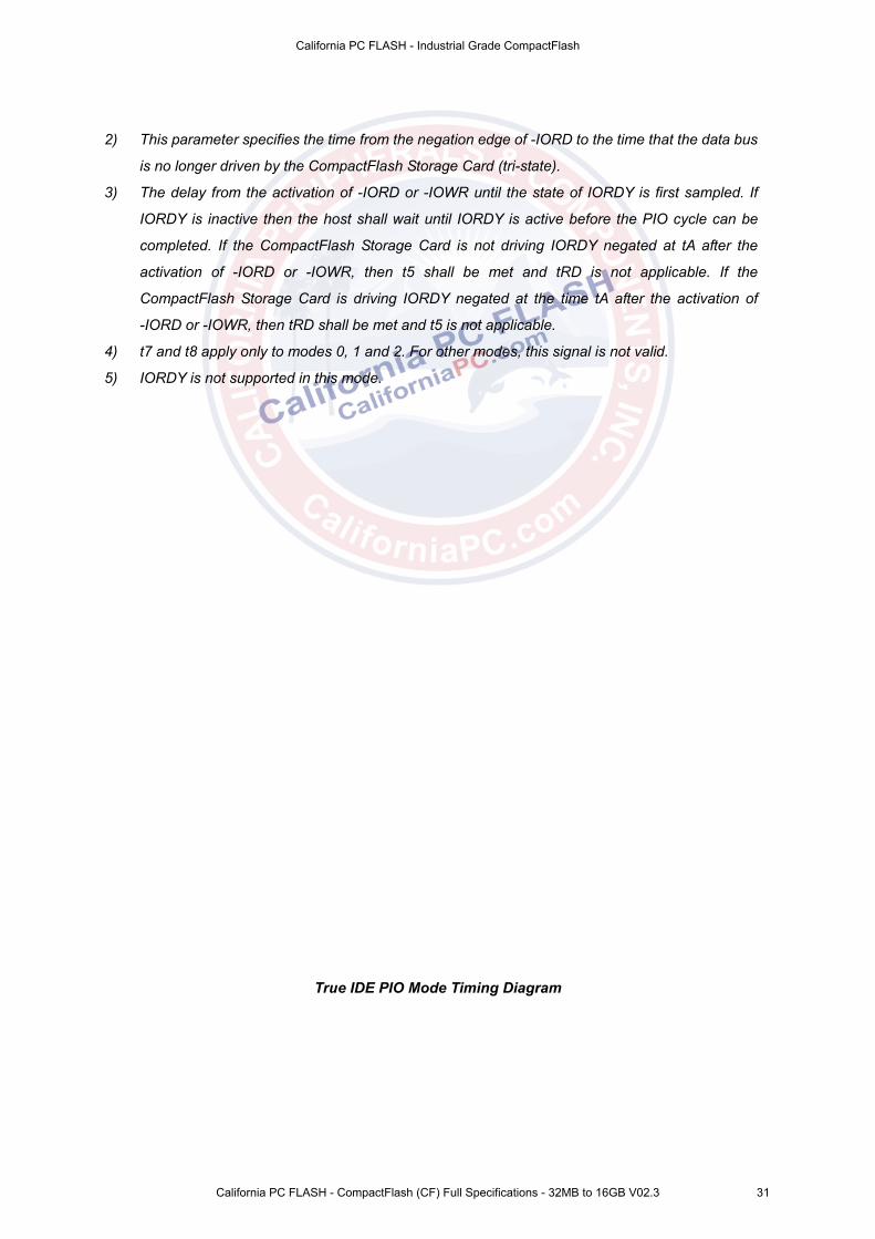
2) This parameter specifies the time from the negation edge of -IORD to the time that the data bus
is no longer driven by the CompactFlash Storage Card (tri-state).
3) The delay from the activation of -IORD or -IOWR until the state of IORDY is first sampled. If
IORDY is inactive then the host shall wait until IORDY is active before the PIO cycle can be
completed. If the CompactFlash Storage Card is not driving IORDY negated at tA after the
activation of -IORD or -IOWR, then t5 shall be met and tRD is not applicable. If the
CompactFlash Storage Card is driving IORDY negated at the time tA after the activation of
-IORD or -IOWR, then tRD shall be met and t5 is not applicable.
4) t7 and t8 apply only to modes 0, 1 and 2. For other modes, this signal is not valid.
5) IORDY is not supported in this mode.
True IDE PIO Mode Timing Diagram
California PC FLASH - Industrial Grade CompactFlash
California PC FLASH - CompactFlash (CF) Full Specifications - 32MB to 16GB V02.3 31

Notes:
(1) Device address consists of CE0, CE1, and HA[2:0]
(2) Data consists of HD[15:00] (16-bit) or HD[7:0] (8 bit)
(3) IOCS16 is shown for PIO modes 0, 1 and 2. For other modes, this signal is ignored.
(4) The negation of IORDY by the device is used to extend the PIO cycle. The determination of
whether the cycle is to be extended is made by the host after tA from the assertion of HIOE or
HIOW. The assertion and negation of IORDY is described in the following three cases:
(4-1) Device never negates IORDY: No wait is generated.
(4-2) Device drives IORDY low before tA: wait generated. The cycle completes after IORDY is
reasserted. For cycles where a wait is generated and HIOE is asserted, the device shall place
read data on D15-D00 for tRD before causing IORDY to be asserted.
California PC FLASH - Industrial Grade CompactFlash
California PC FLASH - CompactFlash (CF) Full Specifications - 32MB to 16GB V02.3 32

6.4.8. True IDE Multiword DMA Mode Read/Write Timing
Item Mode 0 Mode 1 Mode 2 Mode 3 Mode 4 Note
tO Cycle time (min) 480 150 120 100 80 1
tD HIOE / HIOW asserted width (min) 215 80 70 65 55 1
tE HIOE data access (max) 150 60 50 50 45
tF HIOE data hold (min) 5 5 5 5 5
tG HIOE/HIOW data setup (min) 100 30 20 15 10
tH HIOW data hold (min) 20 15 10 5 5
tI DMACK(HREG) to HIOE/HIOW setup
(min) 0 0 0 0 0
tJ HIOE / HIOW to -DMACK hold (min) 20 5 5 5 5
tKR HIOE negated width (min) 50 50 25 25 20 1
tKW HIOW negated width (min) 215 50 25 25 20 1
tLR HIOE to DMARQ delay (max) 120 40 35 35 35
tLW HIOW to DMARQ delay (max) 40 40 35 35 35
tM CEx valid to HIOE / HIOW 50 30 25 10 5
tN CEx hold 15 10 10 10 10
Notes:
t0 is the minimum total cycle time and tD is the minimum command active time, while tKR and tKW
are the minimum command recovery time or command inactive time for input and output cycles
respectively. The actual cycle time equals the sum of the actual command active time and the
actual command inactive time. The three timing requirements of t0, tD, tKR, and tKW shall be met.
The minimum total cycle time requirement is greater than the sum of tD and tKR or tKW.for input
and output cycles respectively. This means a host implementation can lengthen either or both of tD
and either of tKR, and tKW as needed to ensure that t0 is equal to or greater than the value
reported in the device's identify device data. A CompactFlash Storage Card implementation shall
support any legal host implementation.
California PC FLASH - Industrial Grade CompactFlash
California PC FLASH - CompactFlash (CF) Full Specifications - 32MB to 16GB V02.3 33
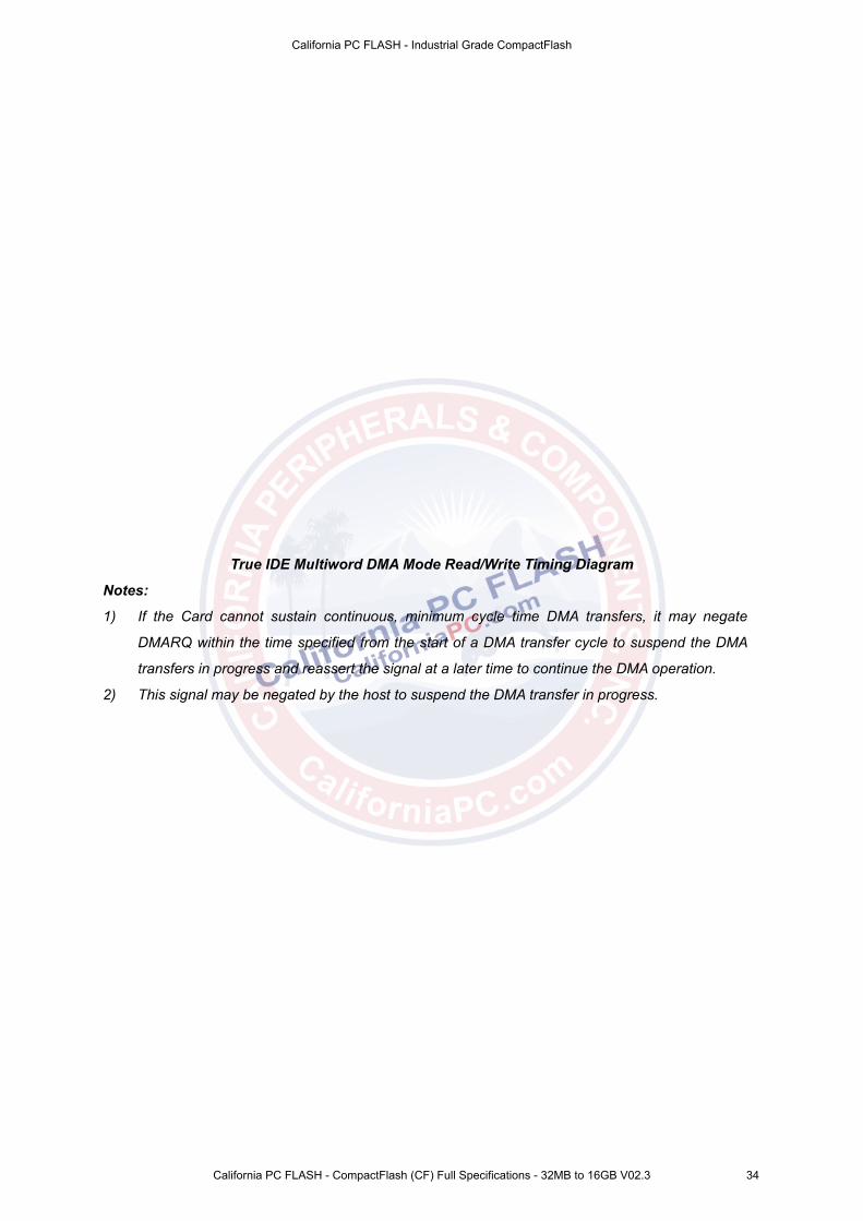
True IDE Multiword DMA Mode Read/Write Timing Diagram
Notes:
1) If the Card cannot sustain continuous, minimum cycle time DMA transfers, it may negate
DMARQ within the time specified from the start of a DMA transfer cycle to suspend the DMA
transfers in progress and reassert the signal at a later time to continue the DMA operation.
2) This signal may be negated by the host to suspend the DMA transfer in progress.
California PC FLASH - Industrial Grade CompactFlash
California PC FLASH - CompactFlash (CF) Full Specifications - 32MB to 16GB V02.3 34

6.4.9. Ultra DMA Signal Usage In Each Interface Mode
Signal Type (Non UDMA
MEM MODE)
PC CARD MEM MODE UDMA
PC CARD IO MODE UDMA
TRUE IDE MODE UDMA
DMARQ Output (-INPACK) -DMARQ -DMARQ DMARQ
HREG Input (-REG) -DMACK DMACK -DMACK
HIOW Input (-IOWR) STOP1 STOP1 STOP1
HIOE Input (-IORD) -HDMARDY(R) 1,2
HSTROBE(W) 1, 3, 4 -HDMARDY(R) 1, 2 HSTROBE(W) 1, 3, 4
-HDMARDY(R) 1, 2 HSTROBE(W)1, 3, 4
IORDY Output (-WAIT) -DDMARDY(W) 1, 3 DSTROBE(R) 1. 2. 4
-DDMARDY(W) 1, 3 DSTROBE(R) 1. 2. 4
-DDMARDY(W) 1, 3 DSTROBE(R) 1. 2. 4
HD[15:00] Bidir (D[15:00]) D[15:00] D[15:00] D[15:00]
HA[10:00] Input (A[10:00]) A[10:00] A[10:00] A[02:00] 5
CSEL Input (-CSEL) -CSEL -CSEL -CSEL
HIRQ Output (READY) READY -INTRQ INTRQ
CE1 CE2 Input (-CE1) (-CE2)
-CE1 -CE2 -CE1 -CE2 -CS0 -CS1
Notes:
1) The UDMA interpretation of this signal is valid only during an Ultra DMA data burst.
2) The UDMA interpretation of this signal is valid only during and Ultra DMA data burst during a
DMA Read command.
3) The UDMA interpretation of this signal is valid only during an Ultra DMA data burst during a
DMA Write command.
4) The HSTROBE and DSTROBE signals are active on both the rising and the falling edge.
5) Address lines 03 through 10 are not used in True IDE mode.
California PC FLASH - Industrial Grade CompactFlash
California PC FLASH - CompactFlash (CF) Full Specifications - 32MB to 16GB V02.3 35

6.4.10. Ultra DMA Data Burst Timing Requirements
UDMA
Mode 0
UDMA
Mode 1
UDMA
Mode 2
UDMA
Mode 3
UDMA
Mode 4
UDMA
Mode 5 Name
Min Max Min Max Min Max Min Max Min Max Min Max
Measure
Location2
t2CYCTYP 240 160 120 90 60 40 Sender
tCYC 112 73 54 39 25 16.8 Note3
t2CYC 230 153 115 86 57 38 Sender
tDS 15.0 10.0 7.0 7.0 5.0 4.0 Recipient
tDH 5.0 5.0 5.0 5.0 5.0 4.6 Recipient
tDVS 70.0 48.0 31.0 20.0 6.7 4.8 Sender
tDVH 6.2 6.2 6.2 6.2 6.2 4.8 Sender
tCS 15.0 10.0 7.0 7.0 5.0 5.0 Device
tCH 5.0 5.0 5.0 5.0 5.0 5.0 Device
tCVS 70.0 48.0 31.0 20.0 6.7 10.0 Host
tCVH 6.2 6.2 6.2 6.2 6.2 10.0 Host
tZFS 0 0 0 0 0 35 Device
tDZFS 70.0 48.0 31.0 20.0 6.7 25 Sender
tFS 230 200 170 130 120 90 Device
tLI 0 150 0 150 0 150 0 100 0 100 0 75 Note4
tMLI 20 20 20 20 20 20 Host
tUI 0 0 0 0 0 0 Host
tAZ 10 10 10 10 10 10 Note5
tZAH 20 20 20 20 20 20 Host
tZAD 0 0 0 0 0 0 Device
tENV 20 70 20 70 20 70 20 55 20 55 20 50 Host
tRFS 75 70 60 60 60 50 Sender
tRP 160 125 100 100 100 85 Recipient
tIORDYZ 20 20 20 20 20 20 Device
tZIORDY 0 0 0 0 0 0 Device
tACK 20 20 20 20 20 20 Host
tSS 50 50 50 50 50 50 Sender
California PC FLASH - Industrial Grade CompactFlash
California PC FLASH - CompactFlash (CF) Full Specifications - 32MB to 16GB V02.3 36

All Timings in ns
1) All timing measurement switching points (low to high and high to low) shall be taken at 1.5 V.
2) All signal transitions for a timing parameter shall be measured at the connector specified in the
measurement location column. For example, in the case of tRFS, both STROBE
and –DMARDY transitions are measured at thesender connector.
3) The parameter tCYC shall be measured at the recipient ’s connector farthest from the sender.
4) The parameter tLI shall be measured at the connector of the sender or recipient that is
responding to an incoming transition from the recipient or sender respectively. Both the
incoming signal and the outgoing response shall be measured at the same connector.
5) The parameter tAZ shall be measured at the connector of the sender or recipient that is driving
the bus but must release the bus to allow for a bus turnaround.
6) See the AC Timing requirements in Table 28: Ultra DMA AC Signal Requirements.
California PC FLASH - Industrial Grade CompactFlash
California PC FLASH - CompactFlash (CF) Full Specifications - 32MB to 16GB V02.3 37

6.4.11. Ultra DMA Data Burst Timing Descriptions
Name Comment Notes
t2CYCTYP Typical sustained average two cycle time
tCYC Cycle time allowing for asymmetry and clock variations (from STROBE edge to
STROBE edge)
t2CYC Two cycle time allowing for clock variations (from rising edge to next rising edge or
from falling edge next falling edge of STROBE)
tDS Data setup time at recipient (from data valid until STROBE edge) 2
tDH Data hold time at recipient (from STROBE edge until data may become invalid) 2
tDVS Data valid setup time at sender (from data valid until STROBE edge) 3
tDVH Data valid hold time at sender (from STROBE edge until data may become invalid) 3
tCS CRC word setup time at device 2
tCH CRC word hold time device 2
tCVS CRC word valid setup time at host (from CRC valid until -DMACK negation) 3
tCVH CRC word valid hold time at sender (from -DMACK negation until CRC may become
invalid) 3
tZFS Time from STROBE output released-to-driving until the first transition of critical
timing.
tDZFS Time from data output released-to-driving until the first transition of critical timing.
tFS First STROBE time (for device to first negate DSTROBE from STOP during a data in
burst)
tLI Limited interlock time 1
tMLI Interlock time with minimum 1
tUI Unlimited interlock time 1
tAZ Maximum time allowed for output drivers to release (from asserted or negated)
tZAH Minimum delay time required for output
tZAD drivers to assert or negate (from released)
tENV Envelope time (from -DMACK to STOP and -HDMARDY during data in burst initiation
and from DMACK to STOP during data out burst initiation)
tRFS Ready-to-final-STROBE time (no STROBE edges shall be sent this long after
negation of -DMARDY)
tRP Ready-to-pause time (that recipient shall wait to pause after negating -DMARDY)
tIORDYZ Maximum time before releasing IORDY
tZIORDY Minimum time before driving IORDY 4
California PC FLASH - Industrial Grade CompactFlash
California PC FLASH - CompactFlash (CF) Full Specifications - 32MB to 16GB V02.3 38

Name Comment Notes
tACK Setup and hold times for -DMACK (before assertion or negation)
tSS Time from STROBE edge to negation of DMARQ or assertion of STOP (when sender
terminates a burst)
Notes:
(1) The parameters tUI, tMLI (in 6.4.17: Ultra DMA Data-In Burst Device Termination Timing and
6.4.18: Ultra DMA Data-In Burst Host Termination Timing), and tLI indicate sender-to-recipient or
recipient-to-sender interlocks, i.e., one agent (either sender or recipient) is waiting for the other
agent to respond with a signal before proceeding. tUI is an unlimited interlock that has no
maximum time value. tMLI is a limited time-out that has a defined minimum. tLI is a limited
time-out that has a defined maximum.
(2) 80-conductor cabling (see ATA specification :Annex A) shall be required in order to meet setup
(tDS, tCS) and hold (tDH, tCH) times in modes greater than 2.
(3) Timing for tDVS, tDVH, tCVS and tCVH shall be met for lumped capacitive loads of 15 and 40 pF at
the connector where the Data and STROBE signals have the same capacitive load value. Due
to reflections on the cable, these timing measurements are not valid in a normally functioning
system.
1) For all timing modes the parameter tZIORDY may be greater than tENV due to the fact that the host
has a pull-up on IORDY- giving it a known state when released.
California PC FLASH - Industrial Grade CompactFlash
California PC FLASH - CompactFlash (CF) Full Specifications - 32MB to 16GB V02.3 39

6.4.12. Ultra DMA Sender and Recipient IC Timing Requirements
UDMA
Mode 0
UDMA
Mode 1
UDMA
Mode 2
UDMA
Mode 3
UDMA
Mode 4
UDMA
Mode 5
UDMA
Mode 6 Name
Min Max Min Max Min Max Min Max Min Max Min Max Min Max
tDSIC 14.7 9.7 6.8 2.3 4.8 2.3 2.3
tDHIC 4.8 4.8 4.8 2.8 4.8 2.8 2.8
tDVSIC 72.9 50.9 33.9 6.0 9.5 6.0 5.2
tDVHIC 9.0 9.0 9.0 6.0 9.0 6.0 5.2
tDSIC Recipient IC data setup time (from data valid until STROBE edge) (see note 2)
tDHIC Recipient IC data hold time (from STROBE edge until data may become invalid) (see note 2)
tDVSIC Sender IC data valid setup time (from data valid until STROBE edge) (see note 3)
tDVHIC Sender IC data valid hold time (from STROBE edge until data may become invalid) (see note 3)
Notes:
1) All timing measurement switching points (low to high and high to low) shall be taken at 1.5 V.
2) The correct data value shall be captured by the recipient given input data with a slew rate of 0.4
V/ns rising and falling and the input STROBE with a slew rate of 0.4 V/ns rising and falling at
tDSIC and tDHIC timing (as measured through 1.5 V).
3) The parameters tDVSIC and tDVHIC shall be met for lumped capacitive loads of 15 and 40 pF
at the IC where all signals have the same capacitive load value. Noise that may couple onto the
output signals from external sources has not been included in these values.
California PC FLASH - Industrial Grade CompactFlash
California PC FLASH - CompactFlash (CF) Full Specifications - 32MB to 16GB V02.3 40

6.4.13. Ultra DMA AC Signal Requirements
Name Comment Min [V/ns] Max [V/ns] Notes
SRISE Rising Edge Slew Rate for any signal 1.25 1
SFALL Falling Edge Slew Rate for any signal 1.25 1
Notes:
1) The sender shall be tested while driving an 18 inch long, 80 conductor cable with PVC
insulation material. The signal under test shall be cut at a test point so that it has not trace,
cable or recipient loading after the test point. All other signals should remain connected through
to the recipient. The test point may be located at any point between the sender’s series
termination resistor and one half inch or less of conductor exiting the connector. If the test point
is on a cable conductor rather than the PCB, an adjacent ground conductor shall also be cut
within one half inch of the connector.
The test load and test points should then be soldered directly to the exposed source side
connectors. The test loads consist of a 15 pF or a 40 pF, 5%, 0.08 inch by 0.05 inch surface
mount or smaller size capacitor from the test point to ground. Slew rates shall be met for both
capacitor values.
Measurements shall be taken at the test point using a <1 pF, >100 Kohm, 1 Ghz or faster probe
and a 500 MHz or faster oscilloscope. The average rate shall be measured from 20% to 80% of
the settled VOH level with data transitions at least 120 nsec apart. The settled VOH level shall
be measured as the average output high level under the defined testing conditions from 100
nsec after 80% of a rising edge until 20% of the subsequent falling edge.
California PC FLASH - Industrial Grade CompactFlash
California PC FLASH - CompactFlash (CF) Full Specifications - 32MB to 16GB V02.3 41

6.4.14. Ultra DMA Data-In Burst Initiation Timing
Ultra DMA Data-In Burst Initiation Timing Diagram
ALL WAVEFORMS IN THIS DIAGRAM ARE SHOWN WITH THE ASSERTED
STATE HIGH. NEGATIVE TRUE SIGNALS APPEAR INVERTED ON THE BUS
RELATIVE TO THE DIAGRAM.
Notes:
The definitions for the IORDY:-DDMARDY:DSTROBE, -IORD:-HDMARDY:HSTROBE, and
-IOWR:STOP signal lines are not in effect until DMARQ and -DMACK are asserted. HA[02:00], -CS0
& -CS1 are True IDE mode signal definitions. HA[10:00], -CE1 and -CE2 are PC Card mode signals.
The Bus polarity of (-) DMACK and (-) DMARQ are dependent on interface mode active.
California PC FLASH - Industrial Grade CompactFlash
California PC FLASH - CompactFlash (CF) Full Specifications - 32MB to 16GB V02.3 42

6.4.15. Sustained Ultra DMA Data-In Burst Timing
Sustained Ultra DMA Data-In Burst Timing Diagram
Notes:
HD[15:00] and DSTROBE signals are shown at both the host and the device to emphasize that cable
settling time as well as cable propagation delay shall not allow the data signals to be considered
stable at the host until some time after they are driven by the device.
California PC FLASH - Industrial Grade CompactFlash
California PC FLASH - CompactFlash (CF) Full Specifications - 32MB to 16GB V02.3 43

6.4.16. Ultra DMA Data-In Burst Host Pause Timing
Ultra DMA Data-In Burst Host Pause Timing Diagram
All waveforms in this diagram are shown with the asserted state high. Negative true
signals appear inverted on the bus relative to the diagram.
Notes:
1) The host may assert STOP to request termination of the Ultra DMA data burst no sooner than
tRP after -HDMARDY is negated.
2) After negating -HDMARDY, the host may receive zero, one, two, or three more data words from
the device.
3) The bus polarity of the (-) DMARQ and (-)DMACK signals is dependent on the active interface
mode.
California PC FLASH - Industrial Grade CompactFlash
California PC FLASH - CompactFlash (CF) Full Specifications - 32MB to 16GB V02.3 44

6.4.17. Ultra DMA Data-In Burst Device Termination Timing
Ultra DMA Data-In Burst Device Termination Timing Diagram
All waveforms in this diagram are shown with the asserted state high. Negative true
signals appear inverted on the bus relative to the diagram.
Notes:
The definitions for the STOP, HDMARDY, and DSTROBE signal lines are no longer in effect after
DMARQ and DMACK are negated. HA[02:00], -CS0 & -CS1 are True IDE mode signal definitions.
HA[10:00], -CE1 and -CE2 are PC Card mode signals. The bus polarity of DMARQ and DMACK are
dependent on the active interface mode.
California PC FLASH - Industrial Grade CompactFlash
California PC FLASH - CompactFlash (CF) Full Specifications - 32MB to 16GB V02.3 45

6.4.18. Ultra DMA Data-In Burst Host Termination Timing
Ultra DMA Data-In Burst Host Termination Timing Diagram
All waveforms in this diagram are shown with the asserted state high. Negative true
signals appear inverted on the bus relative to the diagram.
Notes:
The definitions for the STOP, HDMARDY, and DSTROBE signal lines are no longer in effect after
DMARQ and DMACK are negated. HA[02:00], -CS0 & -CS1 are True IDE mode signal definitions.
HA[10:00],-CE1 and -CE2 are PC Card mode signal definitions. The bus polarity of DMARQ and
DMACK depend on the active interface mode.
California PC FLASH - Industrial Grade CompactFlash
California PC FLASH - CompactFlash (CF) Full Specifications - 32MB to 16GB V02.3 46

6.4.19. Ultra DMA Data-Out Burst Initiation Timing
Ultra DMA Data-Out Burst Initiation Timing Diagram
All waveforms in this diagram are shown with the asserted state high. Negative true
signals appear inverted on the bus relative to the diagram.
Note:
The definitions for the STOP, DDMARDY, and HSTROBE signal lines are not in effect until DMARQ
and DMACK are asserted. HA[02:00], -CS0 & -CS1 are True IDE mode signal definitions. HA[10:00],
-CE1 and -CE2 are PC Card mode signal definitions. The bus polarity of DMARQ and DMACK
depend on the active interface mode.
California PC FLASH - Industrial Grade CompactFlash
California PC FLASH - CompactFlash (CF) Full Specifications - 32MB to 16GB V02.3 47

6.4.20. Sustained Ultra DMA Data-Out Burst Timing
Sustained Ultra DMA Data-Out Burst Timing Diagram
Note:
Data (HD[15:00]) and HSTROBE signals are shown at both the device and the host to emphasize
that cable settling time as well as cable propagation delay shall not allow the data signals to be
considered stable at the device until some time after they are driven by the host.
California PC FLASH - Industrial Grade CompactFlash
California PC FLASH - CompactFlash (CF) Full Specifications - 32MB to 16GB V02.3 48

6.4.21. Ultra DMA Data-Out Burst Device Pause Timing
Ultra DMA Data-Out Burst Device Pause Timing Diagram
All waveforms in this diagram are shown with the asserted state high. Negative true
signals appear inverted on the bus relative to the diagram.
Notes:
1) The device may negate DMARQ to request termination of the Ultra DMA data burst no sooner
than tRP after -DDMARDY is negated.
2) After negating -DDMARDY, the device may receive zero, one, two, or three more data words
from the host.
3) The bus polarity of DMARQ and DMACK depend on the active interface mode.
California PC FLASH - Industrial Grade CompactFlash
California PC FLASH - CompactFlash (CF) Full Specifications - 32MB to 16GB V02.3 49

6.4.22. Ultra DMA Data-Out Burst Device Termination Timing
Ultra DMA Data-Out Burst Device Termination Timing Diagram
All waveforms in this diagram are shown with the asserted state high. Negative true
signals appear inverted on the bus relative to the diagram.
Note:
The definitions for the STOP, DDMARDY, and HSTROBE signal lines are no longer in effect after
DMARQ and DMACK are negated. HA[02:00], -CS0 & -CS1 are True IDE mode signal definitions.
HA[00:10], -CE1 and -CE2 are PC Card mode signals. The bus polarity of DMARQ and DMACK
depend on the active interface mode.
California PC FLASH - Industrial Grade CompactFlash
California PC FLASH - CompactFlash (CF) Full Specifications - 32MB to 16GB V02.3 50

6.4.23. Ultra DMA Data-Out Burst Host Termination Timing
Ultra DMA Data-Out Burst Host Termination Timing Diagram
All waveforms in this diagram are shown with the asserted state high. Negative true
signals appear inverted on the bus relative to the diagram.
Notes:
The definitions for the STOP, DDMARDY, and HSTROBE signal lines are no longer in effect after
DMARQ and DMACK are negated. HA[02:00], -CS0 & -CS1 are True IDE mode signal definitions.
HA[10:00], -CE1 and -CE2 are PC Card mode signal definitions. The bus polarity of DMARQ and
DMACK depend on the active interface mode.
California PC FLASH - Industrial Grade CompactFlash
California PC FLASH - CompactFlash (CF) Full Specifications - 32MB to 16GB V02.3 51

7. CF – ATA Command Description
This section defines the software requirements and the format of the commands the
host sends to the CompactFlashTM Storage Cards. Commands are issued to the
CompactFlashTM Storage Card by loading the required registers in the command
block with the supplied parameters, and then writing the command code to the
Command Register. The manner in which a command is accepted varies. There are
three classes (see Table 37: CF-ATA Command Set) of command acceptance, all
dependent on the host not issuing commands unless the CompactFlashTM Storage
Card is not busy (BSY=0). All commands listed in this specification shall be
implemented. Commands can be implemented as “no operation” to meet this
requirement. The Security Mode feature set (command codes F1, F2, F3, F4, F5, and
F6) should not be implemented unless the device is intended to be used in an
embedded, non-removable application. The Security Mode feature set was not
designed for removable devices and certain problems may be encountered when
using these commands in a removable application. This specification introduces some
new commands and features. If these commands are used on an older CF card, an
Invalid Command Error may occur. Upon receipt of a Class 1 command, the
CompactFlashTM Storage Card sets BSY within 400 nsec. Upon receipt of a Class 2
command, the CompactFlashTM Storage Card sets BSY within 400 nsec, sets up the
sector buffer for a write operation, sets DRQ within 700 µsec, and clears BSY within
400 nsec of setting DRQ. Upon receipt of a Class 3 command, the CompactFlashTM
Storage Card sets BSY within 400 nsec, sets up the sector buffer for a write operation,
sets DRQ within 20 msec (assuming no re-assignments), and clears BSY within 400
nsec of setting DRQ.
California PC FLASH - Industrial Grade CompactFlash
California PC FLASH - CompactFlash (CF) Full Specifications - 32MB to 16GB V02.3 52

7.1. CF – ATA Command Set
Command Code FR SC SN CY DH LBA
Check Power Mode E5 or 98h – – – – Y – Support
Execute Drive Diagnostic 90h – – – – Y – Support
Erase Sector C0h – Y Y Y Y Y Support
Format Track 50h – Y – Y Y Y Support
Identify Device Ech – – – – Y – Support
Idle E3h or 97h – Y – – Y – Support
Idle Immediate E1h or 95h – – – – Y – Support
Initialize Drive Parameters 91h – Y – – Y – Support
NOP 00h – – – – Y – Support
Read Buffer E4h – – – – Y – Support
Read DMA C8h – Y Y Y Y Y Support
Read Multiple C4h – Y Y Y Y Y Support
Read Sector(s) 20h or 21h – Y Y Y Y Y Support
Read Verify Sector(s) 40h or 41h – Y Y Y Y Y Support
Recalibrate 1Xh – – – – Y – Support
Request Sense 03h – – – – Y – Support
Seek 7Xh – – Y Y Y Y Support
Set Feature EFh Y – – – Y – Support
Set Multiple Mode C6h – Y – – Y – Support
Set Sleep Mode E6h or 99h – – – – Y – Support
Standby E2 or 96h – – – – Y – Support
Standby Immediate E0 or 94h – – – – Y – Support
Translate Sector 87h – Y Y Y Y Y Support
Wear Level F5h – – – – Y – Support
Write Buffer E8h – – – – Y – Support
Write DMA CAh – Y Y Y Y Y Support
Write Multiple C5h – Y Y Y Y Y Support
Write Multiple w/o Erase CDh – Y Y Y Y Y Support
Write Sector(s) 30h or 31h – Y Y Y Y Y Support
Write Sector(s) w/o Erase 38h – Y Y Y Y Y Support
Write Verify 3Ch – Y Y Y Y Y Support
California PC FLASH - Industrial Grade CompactFlash
California PC FLASH - CompactFlash (CF) Full Specifications - 32MB to 16GB V02.3 53

Definitions:
FR = Features Register
SC = Sector Count Register (00H-FFH; 00H means 256 sectors)
SN = Sector Number Register
CY = Cylinder Low/High Register
DH = Head No. (0-15) of Drive/Head Register
LBA = Logic Block Address Mode Support
- = Not used for the command
Y = Used for the command
7.2. SMART Command Support
CompactFlashTM Card series supports SMART command set and define some
vendor specific data to report spare/bad block number in each memory
management unit. Users can get the data by “Read Data” command.
SMART Feature Register Values
D0h Read Data D4h Execute OFF-LINE Immediate
D1h Read Attribute Threshold D8h Enable SMART Operations
D2h Enable/Disable Autosave D9h Disable SMART Operations
D3h Save Attribute Values DAh Return Status
Notes: If reserved size below the Threshold, the status can be read from Cylinder register by Return
Status command (DAh).
SMART Data Structure (READ DATA (D0h))
BYTE F / V Decription
0-1 X Revision code
2-361 X Vendor specific
362 V Off line data collection status
363 X Self-test execution status byte
364-365 V Total time in seconds to complete off-line data collection activity
366 X Vendor specific
367 F Off-line data collection capability
368-369 F SMART capability
370 F
Error logging capability
7-1 Reserved
0 1=Device error logging supported
371 X Vendor specific
California PC FLASH - Industrial Grade CompactFlash
California PC FLASH - CompactFlash (CF) Full Specifications - 32MB to 16GB V02.3 54

BYTE F / V Decription
372 F Short self-test routine recommended polling time (in minutes)
373 F Extended self-test routine recommended polling time (in minutes)
374 F Conveyance self-test routine recommended polling time (in minutes)
375-385 R Reserved
386-395 F Firmware Version/Date Code
396 V Number of MU in device (0~n)
397+(n*6) V MU number
398+(n*6) V MU data block
400+(n*6) V MU spare block
401+(n*6) V Init. Bad block
402+(n*6) V Run time Bad block information
511 V Data structure checksum
Notes:
F = the content of the byte is fixed and does not change.
V = the content of the byte is variable and may change depending on the state of the device or the
commands executed by the device.
X = the content of the byte is vendor specific and may be fixed or variable.
R = the content of the byte is reserved and shall be zero.
N = Nth Management Unit
* 4 Byte value : [MSB] [2] [1] [LSB]
California PC FLASH - Industrial Grade CompactFlash
California PC FLASH - CompactFlash (CF) Full Specifications - 32MB to 16GB V02.3 55

7.3. Identify Drive Information(True IDE Mode)
Word
Address
Default
value
Total
Bytes Data Field Type information
0 848Ah 2 General configuration - signature for the CompactFlash Storage Card
1 XXXXh 2 Default number of cylinders
2 0000h 2 Reserved
3 00XXh 2 Default number of heads
4 0000h 2 Obsolete
5 0240h 2 Obsolete
6 XXXXh 2 Default number of sectors per track
7-8 XXXXh 4 Number of sectors per card (Word 7 = MSW, Word 8 = LSW)
9 0000h 2 Obsolete
10-19 XXXXh 20 Serial number in ASCII (Right Justified)
20 0002h 2 Obsolete
21 0002h 2 Obsolete
22 0004h 2 Number of ECC bytes passed on Read/Write Long Commands
23-26 XXXXh 8 Firmware revision in ASCII. Big Endean Byte Order in Word
27-46 XXXXh 40 Model number in ASCII (Left Justified) Big Endean Byte Order in
Word
47 8001h 2 Maximum number of sectors on Read/Write Multiple command
48 0000h 2 Reserved
49 0300h 2 Capabilities
50 0000h 2 Reserved
51 0200h 2 PIO data transfer cycle timing mode
52 0000h 2 Obsolete
53 0007h 2 Field validity
54 XXXXh 2 Current numbers of cylinders
55 XXXXh 2 Current numbers of heads
56 XXXXh 2 Current sectors per track
57-58 XXXXh 4 Current capacity in sectors (LBAs)(Word57=LSW , Word58=MSW)
59 0101h 2 Multiple sector setting
60-61 XXXXh 4 Total number of sectors addressable in LBA Mode
62 0000h 2 Reserved
63 0007h 2 Multiword DMA transfer. In PCMCIA mode this value shall be oh
64 0003h 2 Advanced PIO modes supported
California PC FLASH - Industrial Grade CompactFlash
California PC FLASH - CompactFlash (CF) Full Specifications - 32MB to 16GB V02.3 56

Word
Address
Default
value
Total
Bytes Data Field Type information
65 0078h 2 Minimum Multiword DMA transfer cycle time per word.
66 0078h 2 Recommended Multiword DMA transfer cycle time.
67 0078h 2 Minimum PIO transfer cycle time without flow control
68 0078h 2 Minimum PIO transfer cycle time with lORDY flow control
69-79 0000h 20 Reserved
80 0010h 2 Major version number
81 0000h 2 Minor version number
82 7028h 2 Command sets supported
83 5000h 2 Command sets supported
84 4000h 2 Command sets supported
85 0001h 2 Command sets Enable
86 0000h 2 Command sets Enable
87 0002h 2 Command sets Enable
88 001Fh 2 Ultra DMA support and selected
89 0000h 2 Time required for Security erase unit completion
90 0000h 2 Time required for Enhanced security erase unit completion
91 0000h 2 Current Advanced power management value
92 0000h 2 Master Password Revision Code
93
600Fh
6F00h
603Fh
2
Hardware reset result (Master)
Hardware reset result (Slave)
Hardware reset result (Master w/ slave present)
94-127 0000h 68 Reserved
128 0000h 2 Security status
129-159 0000h 64 vendor unique bytes
160 81F4h 2 Power requirement description
161 0000h 2 Reserved
162 0000h 2 Key management schemes supported
163 0092h 2 CF Advanced True lDE Timing Mode Capability and Setting
164 0000h 2
CF Advanced PCMCIA I/O and Memory Timing Mode Capability and
Setting
80ns cycle in memory and I/O mode
165-175 0000h 22 Reserved
176-255 0000h 140 Reserved
California PC FLASH - Industrial Grade CompactFlash
California PC FLASH - CompactFlash (CF) Full Specifications - 32MB to 16GB V02.3 57

7.4. ID Table Information (PCMCIA Mode)
Word
Address
Default
value
Total
Bytes Data Field Type lnformation
0 848Ah 2 General configuration - signature for the CompactFlash Storage Card
1 XXXXh 2 Default number of cylinders
2 0000h 2 Reserved
3 00XXh 2 Default number of heads
4 0000h 2 Obsolete
5 0240h 2 Obsolete
6 XXXXh 2 Default number of sectors per track
7-8 XXXXh 4 Number of sectors per card (Word 7 = MSW, Word 8 = LSW)
9 0000h 2 Obsolete
10-19 XXXXh 20 Serial number in ASCII (Right Justified)
20 0002h 2 Obsolete
21 0002h 2 Obsolete
22 0004h 2 Number of ECC bytes passed on Read/Write Long Commands
23-26 XXXXh 8 Firmware revision in ASCII. Big Endian Byte Order in Word
27-46 XXXXh 40 Model number in ASCII (Left Justified) Big Endian Byte Order in Word
47 8001h 2 Maximum number of sectors on Read/Write Multiple command
48 0000h 2 Reserved
49 0200h 2 Capabilities
50 0000h 2 Reserved
51 0200h 2 PIO data transfer cycle timing mode
52 0000h 2 Obsolete
53 0003h 2 Field validity
54 XXXXh 2 Current numbers of cylinders
55 XXXXh 2 Current numbers of heads
56 XXXXh 2 Current sectors per track
57-58 XXXXh 4 Current capacity in sectors (LBAs)(Word57=LSW , Word58=MSW)
59 0100h 2 Multiple sector setting
60-61 XXXXh 4 Total number of sectors addressable in LBA Mode
62 0000h 2 Reserved
63 0000h 2 Multiword DMA transfer. In PCMCIA mode this value shall be oh
64 0003h 2 Advanced PIO modes supported
California PC FLASH - Industrial Grade CompactFlash
California PC FLASH - CompactFlash (CF) Full Specifications - 32MB to 16GB V02.3 58

Word
Address
Default
value
Total
Bytes Data Field Type lnformation
65 0000h 2 Minimum Multiword DMA transfer cycle time per word. ln PCMCIA mode
this value shall be 0h
66 0000h 2 Recommended Multiword DMA transfer cycle time. In PCMCIA mode
this value shall be oh
67 0078h 2 Minimum PIO transfer cycle time without flow control
68 0078h 2 Minimum PIO transfer cycle time with lORDY flow control
69-79 0000h 20 Reserved
80 0000h 2 Major version number
81 0000h 2 Minor version number
82 7028h 2 Command sets supported 0
83 500Ch 2 Command sets supported 1
84 4000h 2 Command sets supported 2
85 0001h 2 Command sets Enable 0
86 0000h 2 Command sets Enable 1
87 0000h 2 Command sets Enable 2
88 0000h 2 Ultra DMA supported and selected
89 0000h 2 Time required for Security erase unit completion
90 0000h 2 Time required for Enhanced security erase unit completion
91 0000h 2 Current Advanced power management value
93-127 0000h 70 Reserved
128 0000h 2 Security status
129-159 0000h 64 vendor unique bytes
160 81F4h 2 Power requirement description
161 0000h 2 Reserved
162 0000h 2 Key management schemes supported
163 0000h 2 CF Advanced True lDE Timing Mode Capability and Setting
164 891Bh 2 CF Advanced PCMCIA I/O and Memory Timing Mode Capability and Setting
165-175 0000h 22 Reserved
176-255 0000h 140 Reserved
California PC FLASH - Industrial Grade CompactFlash
California PC FLASH - CompactFlash (CF) Full Specifications - 32MB to 16GB V02.3 59

Identify Drive Information Description
Word 0: General Configuration
This field indicates that the device is a CompactFlashTM Storage Card. Note to host
implementers: If Word 0 of the Identify drive information is 848Ah then the device
complies with the CFA specification, not with the ATA-4 specification.
Word 1: Default Number of Cylinders
This field contains the number of translated cylinders in the default translation mode.
This value will be the same as the number of cylinders.
Word 3: Default Number of Heads
This field contains the number of translated heads in the default translation mode.
Word 6: Default Number of Sectors per Track
This field contains the number of sectors per track in the default translation mode.
Words 7-8: Number of Sectors per Card
This field contains the number of sectors per CompactFlashTM Storage Card. This
double word value is also the first invalid address in LBA translation mode.
Words 10-19: Serial Number
This field contains the serial number for this CompactFlashTM Storage Card and is
right justified and padded with spaces (20h).
Word 22: ECC Count
This field defines the number of ECC bytes used on each sector in the Read and
Write Long commands. This value shall be set to 0004h.
Words 23-26: Firmware Revision
This field contains the revision of the firmware for this product.
Words 27-46: Model Number
This field contains the model number for this product and is left justified and padded
with spaces (20h).
Word 47: Read/Write Multiple Sector Count
Bits 15-8 shall be the recommended value of 80h or the permitted value of 00h.
Bits 7-0 of this word define the maximum number of sectors per block that the
CompactFlashTM Storage Card supports for Read/Write Multiple commands.
California PC FLASH - Industrial Grade CompactFlash
California PC FLASH - CompactFlash (CF) Full Specifications - 32MB to 16GB V02.3 60
Word 49: Capabilities
Bit 13: Standby Timer If bit 13 is set to 1 then the Standby timer is supported as
defined by the IDLE command If bit 13 is set to 0 then the Standby timer operation is
defined by the vendor. Bit 11: IORDY Supported If bit 11 is set to 1 then this
CompactFlashTM Storage Card supports IORDY operation. If bit 11 is set to 0 then this
CompactFlashTM Storage Card may support IORDY operation. Bit 10: IORDY may be
disabled Bit 10 shall be set to 0, indicating that IORDY may not be disabled. Bit 9: LBA
supported Bit 9 shall be set to 1, indicating that this CompactFlashTM Storage Card
supports LBA mode addressing. CF devices shall support LBA addressing. Bit 8:
DMA Supported If bit 8 is set to 1 then Read DMA and Write DMA commands are
supported. Bit 8 shall be set to 0. Read/Write DMA commands are not currently
permitted on CF cards.
Word 51: PIO Data Transfer Cycle Timing Mode
The PIO transfer timing for each CompactFlashTM Storage Card falls into modes that
have unique parametric timing specifications. The value returned in Bits 15-8 shall be
00h for mode 0, 01h for mode 1, or 02h for mode 2. Values 03h through FFh are
reserved.
Word 53: Translation Parameters Valid
Bit 0 shall be set to 1 indicating that words 54 to 58 are valid and reflect the current
number of cylinders, heads and sectors. If bit 1 of word 53 is set to 1, the values in
words 64 through 70 are valid. If this bit is cleared to 0, the values reported in words
64-70 are not valid. Any CompactFlashTM Storage Card that supports PIO mode 3 or
above shall set bit 1 of word 53 to one and support the fields contained in words 64
through 70.
Words 54-56: Current Number of Cylinders, Heads, Sectors/Track
These fields contain the current number of user addressable Cylinders,
Heads, and Sectors/Track in the current translation mode.
Words 57-58: Current Capacity
This field contains the product of the current cylinders times heads times sectors.
Word 59: Multiple Sector Setting
Bits 15-9 are reserved and shall be set to 0. Bit 8 shall be set to 1 indicating that the
Multiple Sector Setting is valid. Bits 7-0 are the current setting for the number of
sectors that shall be transferred per interrupt on Read/Write Multiple commands.
Words 60-61: Total Sectors Addressable in LBA Mode
This field contains the total number of user addressable sectors for the
CompactFlashTM Storage Card in LBA mode only.
California PC FLASH - Industrial Grade CompactFlash
California PC FLASH - CompactFlash (CF) Full Specifications - 32MB to 16GB V02.3 61

Word 64: Advanced PIO transfer modes supported
Bits 7 through 0 of word 64 of the Identify Device parameter information is defined as
the advanced PIO data transfer supported field. If this field is supported, bit 1 of word
53 shall be set to one. This field is bit significant. Any number of bits may be set to one
in this field by the CompactFlashTM Storage Card to indicate the advanced PIO modes
it is capable of supporting. Of these bits, bits 7 through 2 are reserved for future
advanced PIO modes. Bit 0, if set to one, indicates that the CompactFlashTM Storage
Card supports PIO mode 3. Bit 1, if set to one, indicates that the CompactFlashTM
Storage Card supports PIO mode 4.
Word 67: Minimum PIO transfer cycle time without flow control
Word 67 of the parameter information of the Identify Device command is defined as
the minimum PIO transfer without flow control cycle time. This field defines, in
nanoseconds, the minimum cycle time that, if used by the host, the CompactFlashTM
Storage Card guarantees data integrity during the transfer without utilization of flow
control. If this field is supported, Bit 1 of word 53 shall be set to one. Any
CompactFlashTM Storage Card that supports PIO mode 3 or above shall support this
field, and the value in word 67 shall not be less than the value reported in word 68. If
bit 1 of word 53 is set to one because a CompactFlashTM Storage Card supports a
field in words 64-70 other than this field and the CompactFlashTM Storage Card does
not support this field, the CompactFlashTM Storage Card shall return a value of zero in
this field.
Word 68: Minimum PIO transfer cycle time with IORDY
Word 68 of the parameter information of the Identify Device command is defined as
the minimum PIO transfer with IORDY flow control cycle time. This field defines, in
nanoseconds, the minimum cycle time that the CompactFlashTM Storage Card
supports while performing data transfers while utilizing IORDY flow control. If this field
is supported, Bit 1 of word 53 shall be set to one. Any CompactFlashTM Storage Card
that supports PIO mode 3 or above shall support this field, and the value in word 68
shall be the fastest defined PIO mode supported by the CompactFlashTM Storage
Card. If bit 1 of word 53 is set to one because a CompactFlashTM Storage Card
supports a field in words 64-70 other than this field and the CompactFlashTM Storage
Card does not support this field, the CompactFlashTM Storage Card shall return a
value of zero in this field.
California PC FLASH - Industrial Grade CompactFlash
California PC FLASH - CompactFlash (CF) Full Specifications - 32MB to 16GB V02.3 62

Words 82-84: Features/command sets supported
Words 82, 83, and 84 shall indicate features/command sets supported. The value
0000h or FFFFh was placed in each of these words by CompactFlashTM Storage
Cards prior to ATA-3 and shall be interpreted by the host as meaning that
features/command sets supported are not indicated. Bits 1 through 13 of word 83 and
bits 0 through 13 of word 84 are reserved. Bit 14 of word 83 and word 84 shall be set
to one and bit 15 of word 83 and word 84 shall be cleared to zero to provide indication
that the features/command sets supported words are valid. The values in these words
should not be depended on by host implementers. Bit 0 of word 82 shall be set to zero;
the SMART feature set is not supported. If bit 1 of word 82 is set to one, the Security
Mode feature set is supported. Bit 2 of word 82 shall be set to zero; the Removable
Media feature set is not supported. Bit 3 of word 82 shall be set to one; the Power
Management feature set is supported. Bit 4 of word 82 shall be set to zero; the Packet
Command feature set is not supported. If bit 5 of word 82 is set to one, write cache is
supported. If bit 6 of word 82 is set to one, look-ahead is supported. Bit 7 of word 82
shall be set to zero; release interrupt is not supported. Bit 8 of word 82 shall be set to
zero; Service interrupt is not supported. Bit 9 of word 82 shall be set to zero; the
Device Reset command is not supported. Bit 10 of word 82 shall be set to zero; the
Host Protected Area feature set is not supported. Bit 11 of word 82 is obsolete. Bit 12
of word 82 shall be set to one; the CompactFlashTM Storage Card supports the Write
Buffer command. Bit 13 of word 82 shall be set to one; the CompactFlashTM Storage
Card supports the Read Buffer command. Bit 14 of word 82 shall be set to one; the
CompactFlashTM Storage Card supports the NOP command.
Bit 15 of word 82 is obsolete. Bit 0 of word 83 shall be set to zero; the
CompactFlashTM Storage Card does not support the Download Microcode command.
Bit 1 of word 83 shall be set to zero; the CompactFlashTM Storage Card does not
support the Read DMA Queued and Write DMA Queued commands. Bit 2 of word 83
shall be set to one; the CompactFlashTM Storage Card supports the CFA feature set. If
bit 3 of word 83 is set to one, the CompactFlashTM Storage Card supports the
Advanced Power Management feature set. Bit 4 of word 83 shall be set to zero; the
CompactFlashTM Storage Card does not support the Removable Media Status feature
set.
California PC FLASH - Industrial Grade CompactFlash
California PC FLASH - CompactFlash (CF) Full Specifications - 32MB to 16GB V02.3 63

Words 85-87: Features/command sets enabled
Words 85, 86, and 87 shall indicate features/command sets enabled. The value
0000h or FFFFh was placed in each of these words by CompactFlashTM Storage
Cards prior to ATA-4 and shall be interpreted by the host as meaning that
features/command sets enabled are not indicated. Bits 1 through 15 of word 86 are
reserved. Bits 0-13 of word 87 are reserved. Bit 14 of word 87 shall be set to one and
bit 15 of word 87 shall be cleared to zero to provide indication that the
features/command sets enabled words are valid. The values in these words should
not be depended on by host implementers. Bit 0 of word 85 shall be set to zero; the
SMART feature set is not enabled. If bit 1 of word 85 is set to one, the Security Mode
feature set has been enabled via the Security Set Password command. Bit 2 of word
85 shall be set to zero; the Removable Media feature set is not supported. Bit 3 of
word 85 shall be set to one; the Power Management feature set is supported. Bit 4 of
word 85 shall be set to zero; the Packet Command feature set is not enabled. If bit 5
of word 85 is set to one, write cache is enabled. If bit 6 of word 85 is set to one,
look-ahead is enabled. Bit 7 of word 85 shall be set to zero; release interrupt is not
enabled. Bit 8 of word 85 shall be set to zero; Service interrupt is not enabled. Bit 9 of
word 85 shall be set to zero; the Device Reset command is not supported. Bit 10 of
word 85 shall be set to zero; the Host Protected Area feature set is not supported. Bit
11 of word 85 is obsolete. Bit 12 of word 85 shall be set to one; the CompactFlashTM
Storage Card supports the Write Buffer command. Bit 13 of word 85 shall be set to
one; the CompactFlashTM Storage Card supports the Read Buffer command. Bit 14 of
word 85 shall be set to one; the CompactFlashTM Storage Card supports the NOP
command.
Bit 15 of word 85 is obsolete. Bit 0 of word 86 shall be set to zero; the
CompactFlashTM Storage Card does not support the Download Microcode command.
Bit 1 of word 86 shall be set to zero; the CompactFlashTM Storage Card does not
support the Read DMA Queued and Write DMA Queued commands. If bit 2 of word
86 shall be set to one, the CompactFlashTM Storage Card supports the CFA feature
set. If bit 3 of word 86 is set to one, the Advanced Power Management feature set has
been enabled via the Set Features command. Bit 4 of word 86 shall be set to zero; the
CompactFlashTM Storage Card does not support the Removable Media Status feature
set.
Word 89: Time required for Security erase unit completion
Word 89 specifies the time required for the Security Erase Unit command to
complete. This command shall be supported on CompactFlashTM Storage Cards
that support security.
California PC FLASH - Industrial Grade CompactFlash
California PC FLASH - CompactFlash (CF) Full Specifications - 32MB to 16GB V02.3 64

Value Time
0 Value not specified
1-254 (Value * 2) minute
255 >508 minutes
Word 90: Time required for Enhanced security erase unit completion
Word 90 specifies the time required for the Enhanced Security Erase Unit command
to complete. This command shall be supported on CompactFlashTM Storage Cards
that support security.
Value Time
0 Value not specified
1-254 (Value * 2) minutes
255 >508 minutes
Word 91: Advanced power management level value
Bits 7-0 of word 91 contain the current Advanced Power Management level setting.
Word 128: Security Status
Bit 8: Security Level
If set to 1, indicates that security mode is enabled and the security level is maximum.
If set to 0 and security mode is enabled, indicates that the security level is high.
Bit 5: Enhanced security erase unit feature supported
If set to 1, indicates that the Enhanced security erase unit feature set is supported.
Bit 4: Expire
If set to 1, indicates that the security count has expired and Security Unlock and
Security Erase
Unit are command aborted until a power-on reset or hard reset.
Bit 3: Freeze
If set to 1, indicates that the security is Frozen.
Bit 2: Lock
If set to 1, indicates that the security is locked.
Bit 1: Enable/Disable
If set to 1, indicates that the security is enabled.
If set to 0, indicates that the security is disabled.
Bit 0: Capability If set to 1, indicates that CompactFlashTM Storage Card supports
security mode feature set. If set to 0, indicates that CompactFlashTM Storage Card
does not support security mode feature set.
California PC FLASH - Industrial Grade CompactFlash
California PC FLASH - CompactFlash (CF) Full Specifications - 32MB to 16GB V02.3 65

Word 160: Power Requirement Description
This word is required for CompactFlashTM Storage Cards that support power mode 1.
Bit 15: VLD
If set to 1, indicates that this word contains a valid power requirement description.
If set to 0, indicates that this word does not contain a power requirement description.
Bit 14: RSV
This bit is reserved and must be 0.
Bit 13: -XP
If set to 1, indicates that the CompactFlashTM Storage Card does not have Power
Level 1
commands.
If set to 0, indicates that the CompactFlashTM Storage Card has Power Level 1
commands
Bit 12: -XE
If set to 1, indicates that Power Level 1 commands are disabled.
If set to 0, indicates that Power Level 1 commands are enabled.
Bit 0-11: Maximum current
This field contains the CompactFlashTM Storage Card’s maximum current in mA.
Word 162: Key Management Schemes Supported
Bit 0: CPRM support
If set to 1, the device supports CPRM Scheme (Content Protection for Recordable
Media)
If set to 0, the device does not support CPRM.
Bits 1-15 are reserved for future additional Key Management schemes.
California PC FLASH - Industrial Grade CompactFlash
California PC FLASH - CompactFlash (CF) Full Specifications - 32MB to 16GB V02.3 66

APPENDIX
A. Ordering Information 1. Part Numbers
Capacity Commercial Temperature (0º to +70º)
Industrial Temperature (-40º to +85º)
16MB FCF-16MB-X1X2XX FCFI-16MB-X1X2XX32MB FCF-32MB-X1X2XX FCFI-32MB-X1X2XX64MB FCF-64MB-X1X2XX FCFI-64MB-X1X2XX128MB FCF-128MB-X1X2XX FCFI-128MB-X1X2XX256MB FCF-256MB-X1X2XX FCFI-256MB-X1X2XX512MB FCF-512MB-X1X2XX FCFI-512MB-X1X2XX1GB FCF-01GB-X1X2XX FCFI-01GB-X1X2XX2GB FCF-02GB-X1X2XX FCFI-02GB-X1X2XX4GB FCF-04GB-X1X2XX FCFI-04GB-X1X2XX8GB FCF-08GB-X1X2XX FCFI-08GB-X1X2XX16GB FCF-16GB-X1X2XX FCFI-16GB-X1X2XX
1) X1: Transfer mode: 2 = (PIO 4), 3 = DMA 2 (Multi Word), 4 = UDMA 4 (UltraDMA)
2) X2: Disk mode: 1 = Removable Disk, 2 = Fixed Disk, 3 = Auto Detect Disk
*Available Options:
*Other options available upon request
Warranty is 3 Years
32MB to 2GB -2132 = Removable, PIO 4 -2232 = Fixed, PIO 4 -3232 = Fixed, DMA2 -3332 = Auto Detect, DMA 2-4132 = Removable, UDMA 4 -4232 = Fixed, UDMA 4 -4332 = Auto Detect, UDMA 4
4GB to 16GB -2133 = Removable, PIO 4 -2233 = Fixed, PIO 4 -3233 = Fixed, DMA2 -3333 = Auto Detect, DMA 2 -4133 = Removable, UDMA 4 -4233 = Fixed, UDMA 4 -4333 = Auto Detect, UDMA 4
California PC FLASH - Industrial Grade CompactFlash
California PC FLASH - CompactFlash (CF) Full Specifications - 32MB to 16GB V02.3 67

California PC FLASH is available for purchase online from www.CaliforniaPC.com as well as from several dealers in the U.S. and WorldWide.
California PC FLASH Division of California Peripherals & Components, Inc. 216 Avenida Fabricante, Ste 108 San Clemente, CA 92672 USA
Tel: 1-949-487-1213 FAX: 1-949-487-1866
Toll Free: 1-877-487-1213
California PC FLASH - Industrial Grade CompactFlash
California PC FLASH - CompactFlash (CF) Full Specifications - 32MB to 16GB V02.3 68