Cadence OrCAD PCB Designer - School of...
47
Electronic Design Project 2 Cadence OrCAD PCB Designer 16.2 Professor John H. Davies 2010 January 25 Objectives After completing these laboratories, you should be able to: • analyse by hand, capture, simulate and lay out a simple, one-transistor amplifier on a one-sided printed circuit board (PCB) with manual routing • lay out an instrumentation amplifier based on three op-amps, comparing one-sided and double-sided boards with automatic routing, and produce photomasks for pro- duction • lay out a mixed-signal system, comparable with the final project in this course, fol- lowing standard procedures for schematic capture. Preamble Please ensure that you have the following two items for every laboratory. • A bound, A4 laboratory notebook for recording your results and making notes. You will get no marks if you don’t have a book with you. • University (Novell) printer credits so that you can print the circuits, layouts and the results of your simulations. Printouts should be attached firmly into your laboratory book for future reference. The first part of these laboratories, which is a ‘pencil and paper’ analysis of a one-transistor amplifier, must be written up in your laboratory book as you do it. The remaining parts do not need much of a record to be kept but you will find it useful to make a note of tricks and tips for using OrCAD. This will be valuable when you have to design your own circuits later this year and in subsequent projects. These laboratories form part of your professional development because it is expected that every electronic engineer should be able to design, populate and test a printed circuit board (PCB). You must therefore complete the first two designs to be awarded credit. Most of the marks are awarded simply for completion but extra marks will be awarded for good layouts. Late work will be considered for credit but marks will not be awarded. 1
Transcript of Cadence OrCAD PCB Designer - School of...

Electronic Design Project 2Cadence OrCAD PCB Designer 16.2
Professor John H. Davies
2010 January 25
Objectives
After completing these laboratories, you should be able to:
• analyse by hand, capture, simulate and lay out a simple, one-transistor amplifier ona one-sided printed circuit board (PCB) with manual routing
• lay out an instrumentation amplifier based on three op-amps, comparing one-sidedand double-sided boards with automatic routing, and produce photomasks for pro-duction
• lay out a mixed-signal system, comparable with the final project in this course, fol-lowing standard procedures for schematic capture.
PreamblePlease ensure that you have the following two items for every laboratory.
• A bound, A4 laboratory notebook for recording your results and making notes. You willget no marks if you don’t have a book with you.
• University (Novell) printer credits so that you can print the circuits, layouts and the resultsof your simulations. Printouts should be attached firmly into your laboratory book forfuture reference.
The first part of these laboratories, which is a ‘pencil and paper’ analysis of a one-transistoramplifier, must be written up in your laboratory book as you do it. The remaining parts do notneed much of a record to be kept but you will find it useful to make a note of tricks and tips forusing OrCAD. This will be valuable when you have to design your own circuits later this yearand in subsequent projects.
These laboratories form part of your professional development because it is expected thatevery electronic engineer should be able to design, populate and test a printed circuit board(PCB). You must therefore complete the first two designs to be awarded credit. Most of themarks are awarded simply for completion but extra marks will be awarded for good layouts.Late work will be considered for credit but marks will not be awarded.
1

Contents1 Introduction 2
2 One-transistor amplifier: simple analysis 4
3 Schematic capture and simulation 6
4 Preparation for PCB layout 9
5 OrCAD PCB Editor 17
6 Instrumentation amplifier – single-sided board 27
7 Instrumentation amplifier – double-sided board 38
8 A mixed-signal system 41
A How to correct a layout if you spot an error in the circuit 45
B Summary: PCB design flow 46
1 IntroductionThese exercises introduce you to schematic capture, simulation and PCB layout using CadenceOrCAD PCB Designer with PSpice. This suite comprises three main applications.
• Capture is used to draw the circuit on the screen (schematic capture). It is easy toincorporate changes to the design and to correct errors. (On the other hand, it is muchfaster to develop the outline of a circuit using pencil and paper, as we shall do for the firstexercise.)
• PSpice simulates a captured circuit and confirm that it performs as specified. Plots wereproduced by a separate application called Probe in the past and I’ll stick to this name,although this functionality has long been integrated into PSpice.
• PCB Editor (Allegro) is the application for laying out a printed circuit board. Thisincludes an automatic router (SPECCTRA) that works out the arrangement of tracksneeded to connect your components on the PCB. The output is a set of files that can besent to a manufacturer or printouts for the electronics workshop in the Rankine Building.
The first two applications should be familiar from last year but the third is new. These programsare accessed via networked Windows PCs in the department, with up to 40 users at any onetime. Unfortunately the licensing arrangements do not permit access from outwith the RankineBuilding. A demonstration version on DVD is available; please ask.
OrCAD PCB Designer is the most basic version of Cadence’s Allegro suite for PCB designand much of the documentation refers to ‘Allegro’ rather than ‘PCB Editor’. Allegro is widelyused in industry and is similar to the Cadence software for laying out integrated circuits (ICs),which you will experience in Digital Circuit Design 3.
2

Fixup. I have encountered various problems with the software, mainly due to incompatibilitiesbetween the libraries supplied for Capture and those for PCB Editor. These are marked asFixups. I hope that we will find smoother ways around these difficulties in the future. I’d alsobe grateful for suggestions for improving these instructions. ¦
1.1 Libraries, files, directories and design rulesPCB Designer uses and creates a large number of files and libraries. It is essential to keep thesein the expected locations. Three types of information are needed for each component.
• Electrical symbols are used to draw the circuit in Capture.
• Electrical models allow you to simulate the circuit in PSpice.
• Footprints or package symbols show the physical size and shapes of the pads (wherethe pins are soldered to the board) and the outline of the package. They are used to layout the circuit in PCB Editor.
These are stored in different sets of libraries and you must select the files needed for a particulardesign. You might wonder why footprints are needed as well as electrical symbols. The reasonis that components with the same electrical behaviour come in different packages. For example,an integrated circuit might come in two versions:
• a traditional, plastic dual-in-line package (PDIP) with pins 0.1′′ apart
• a smaller, surface-mount device (SMD) with pins only 0.5 mm apart, if it has pins at all
The opposite is also true: resistors of a particular shape come in a wide range of values.Further information is needed to describe the characteristics of the printed circuit board on
which the components are mounted. The details are important for high-speed designs but weneed to know only the number of layers of copper, called etch in PCB Designer. This tutorialcovers only single-sided boards, which have components on top and copper on the bottom,and double-sided boards, which have copper on both surfaces but components only on the top.Fancier boards often have two internal planes of copper used for power and ground; complexdesigns need further layers.
Design rules are required to lay out the circuit on the PCB. The full details are complex butthe basic rules specify the minimum width of tracks and the gap between them. Manufacturersoften express these numbers in the format 10/8, meaning minimum widths of 10 for tracks and8 for gaps (although the numbers are usually the same). The units are almost always mils,which mean thousands of an inch; see section 4.4 on page 13. We use 25/25 rules, which areextremely coarse but produce boards that are easy for inexperienced students to solder.
1.2 Help!Extensive documentation is provided with OrCAD. Please try this before asking a demonstrator– it is part of the learning process. Most professional software is so complicated that evenexperts make regular use of the help files. An unhelpful feature of the Cadence help systemis that it opens only with the page associated with the most recent action rather than offering
3

Figure 1. Cadence Help system with the Navigation pane opened.
the full range of documents. Go to the menu bar of the Cadence Help page and choose View >Navigation > Show, which produces a screen like that in figure 1. Use the navigation panel onthe left to choose the appropriate product and type the desired topic into the Topics box.
You should know this by now but a reminder is never a bad idea: Save your work fre-quently and take regular backups of important circuits.
2 One-transistor amplifier: simple analysisFigure 2 shows the circuit of a simple amplifier with one transistor. It is intended to amplifyaudio signals, say from 20 Hz – 20 kHz. Always make a rough design of a circuit using penciland paper before simulating it. You will not learn how to design this particular circuit untilthe Analogue Electronics 2 course later in year, so we shall ‘reverse engineer’ it instead. Thecalculations are simple and should be done in your laboratory book. You should be pleasantlysurprised to find that you don’t need to know much about transistors to analyse this. In fact youdid most of it in Electronic Engineering 1Y. Make sure that you recognise the emitter, base andcollector of the transistor.
We first find the bias point, also called the operating point or quiescent point. This meansthe conditions when no signal is applied and the circuit is ‘resting’. The 10 mVac source cantherefore be ignored.
4

Figure 2. A simple, one-transistor amplifier that can be simulated using Spice.
1. Resistors R1 and R2 form a simple potential divider if we ignore the other componentsattached to them. (We should go back and check this assumption when the currents areknown.) Calculate the voltage on the base of the transistor Q1.
2. The base–emitter junction of a transistor is a forward-biassed diode (hence the arrow onits symbol) and therefore has a voltage of Vbe ≈ 0.7V across it. Use this to calculate thevoltage on the emitter.
3. We now know the voltage across the resistor R4. Calculate the current through it.
4. The current into the base of a transistor is much smaller than the other two currents, sothe current flowing into the collector is nearly equal to that flowing out of the emitter.Calculate the voltage dropped across R3 and hence the voltage on the collector.
This has shown why the four resistors are needed but not the capacitors. What is the expressionfor the impedance of a capacitor (remember that it is complex) and how does its magnitudedepend on frequency? The capacitors in this circuit allow high frequencies to pass – the signalsthat we wish to amplify – but block the steady voltages that set the bias point.
• We have seen that the base of the transistor is kept at a particular voltage by the potentialdivider, which sets the bias point. The capacitor C1 on the input isolates this voltage fromthe previous stage of the system but lets the signal through.
• Look at the circuit through which the input signal flows. It passes ‘through’ the capacitorC1, the base–emitter junction of the transistor, R4 and C2 in parallel, and back to theground connection of the input. Only the part of the voltage across the base–emitterjunction gets amplified; the rest is wasted and should therefore be made as small aspossible. This means that we would like to get rid of R4 but this cannot be done becauseit is needed to set the bias point – it determines the current through the transistor, as yousaw above.
5

The solution is to put the bypass capacitor C2 across the resistor. The bias has zerofrequency so it all flows through the resistor. The signal has a ‘high’ frequency so mostof it flows through the capacitor, which must therefore have a much smaller impedancethan the resistor.
Ideally the impedance of C2 should obey |ZC( f )| � R4 for all frequencies in the signal. Is thistrue for the values in figure 2?
Finally, we should estimate the voltage gain of the circuit. This needs some background ontransistors that you have not yet covered so I’ll just quote the result. The gain is given by
VoutVin
=−gmR3 (1)
where gm is called the transconductance of the transistor, defined by ∂ Ic/∂Vbe. Its value isgiven by
gm =Ic
VT(2)
where Ic is the collector current at the bias point, which you have calculated already, and VTis called the thermal voltage. This is in turn given by VT = kBT/e where kB is Boltzmann’sconstant (remember this from physics courses?), T is the absolute temperature and e is themagnitude of the electronic charge. Don’t worry about the formula because VT≈ 25mV at roomtemperature, which isn’t too hard to remember. Now you can calculate the transconductanceand voltage gain. Express the gain both as a ratio and in decibels (dB).
* Milestone: Show your results to a member of staff and be prepared to explain them.
An interesting feature is that we haven’t used any details of the transistor at all! This makesit easy to design circuits based on bipolar junction transistors, to give them their full name.
Now we’ll capture the circuit in OrCAD, simulate it and check these estimates.
3 Schematic capture and simulationAlways create a fresh directory for every new project in OrCAD otherwise you will en-counter strange errors, from which it seems impossible to recover. It also keeps your workorganised.
Select Start > Programs > OrCAD 16.2 > OrCAD Capture. I use ‘>’ throughout thisdocument to show the levels of a hierarchical menu. There will be a short delay while thesoftware is loaded and the licence server is accessed. Alternatively, you will be asked if youwish to use Demo mode if no licence can be found. You may be offered a Cadence ProductChoices box, in which case you should choose OrCAD PCB Designer with PSpice. Thescreen eventually shows the OrCAD Capture main window with a menu bar and tool bar. Asub-window at the bottom shows the session log.
3.1 Create a projectThe first step in any design is always to create a project in OrCAD.
6

1. Create a new directory in Windows to hold all files for the project.
2. Select File > New > Project from the menu bar of Capture.
3. In the New Project dialog box:
• Select an Analog or Mixed A/D project. This choice is essential or you will not beable to simulate the circuit.
• Click on the Browse key, select your H drive and navigate to the new directory thatyou created for this design. Click OK.
• Give the project a meaningful name.
• The path and directory now show in the location box (if you can see them – theyare usually too long). Click OK in the New Project dialog box.
• Click Next.
4. Select the Create a blank project button in the small dialog box that appears and clickOK.
5. Your project will now be created. The Project Manager window at the top left shows thefiles associated with your design and the resources used, such as library files. Its title isthe full pathname of your project, which is usually far too long to fit. Check that the Filetab is selected if the view looks unfamiliar.
6. Expand the Design Resources folder in the project, then the design (called ./project-name.dsn, where project-name is the name of your project), then the SCHEMATIC1folder and finally double-click PAGE1 to open the schematic page for your design. Lo-cate the Title box in the lower right-hand corner, double-click on the placeholders, whichare in angle brackets <>, and replace them with a descriptive title and so on.
3.2 Draw the circuitLay out the circuit in figure 2 on page 5. The method is exactly the same as last year but hereare a few tips in case you have forgotten. The names of the components are listed in table 1 onpage 12. I’ve renamed some of them to make their functions clearer.
Jargon: The label that identifies each component on the schematic drawing is called its refer-ence or refdes, short for reference designator. For example, the transistor has refdes Q1. Eachrefdes must be unique: No other component can be called Q1. ¦
• All circuits must have a ground node called 0 (zero) for simulation. Get it with Place >Ground. . . from the menu bar or from the ground button on the right.
• PSpice is unhelpful about notation. Usage like 10ˆ6 doesn’t work but it won’t tell you!(It will just stop at the caret and take the value as 10.) Use 1e6 or 1Meg instead – not 1Mbecause a single m or M means milli, not mega.
7

• Libraries must be chosen from the pspice folder, otherwise the components will not havePSpice models and you will not be able to simulate them.
• Basic components like resistors are in the analog library, sources such as VDC are insource and the param block is in special. Use Search if you can’t guess where a com-ponent is located. You will probably need to do this for the transistor.
• The capacitor C2 is an electrolytic type, which must be installed with the correct polarityor it will explode. Its parameter CMAX is the maximum working voltage, which is notneeded for simulation but important when you pick out a real component. Set it to 16 V,which is a common value.
• Always join components with wires, not by placing them so close that their pins overlap.
• Wires and components sometimes become joined incorrectly if you move them about.Use Place > Junction or the junction tool from the buttons on the right to eliminatespurious connections.
• Place Voltage Level Markers on the points on the circuit where you want to plot thevalues. This is easier than selecting them from the list of variables in Probe.
• I like to use off-page connectors to label nodes such as input and output, where thevoltages will be plotted. Place them from the menu or button. The names appear inProbe and make it much easier to identify the traces.
3.3 Simulate the circuitSet up a Simulation Profile to make an AC Sweep of the circuit from 10 Hz to 100 kHz. Re-member that the sweep should be logarithmic in decades, not linear. About 10 points perdecade should be adequate. Run the simulation and plot the results. First, check that the biaspoint agrees with the pencil-and-paper calculations. Go back to Capture and click the V buttonto Enable Bias Voltage Display. Check the current through the transistor too.
Next, plot the voltage gain in decibels (dB) rather than the output voltage itself. You shouldremember how to do this from the RC filter last year but here is a reminder.
1. Delete all the traces in the plot window.
2. Choose Trace > Add Trace from the menu bar. The dialog box shows variables on theleft and functions on the right.
3. Choose the DB function from the right and insert the output voltage divided by theinput voltage using the variables from the left. The final expression should look likeDB(V(Output)/V(Input)) if you used the same names as me.
Does the gain match the estimated value? Is it reasonably constant with frequency across theaudio range?
I found that the gain did not behave as expected (so now I have given you the answer tothe first question!) and suspect that the capacitor C2 across the emitter resistor R4 is too small.Check this by simulating the circuit for a set of values of C2. This requires a parameter. Youshould remember how to do this but the procedure is clumsy so here is a reminder.
8
1. First place a param block on your schematic from the special library.
2. Open the Property Editor for the param block with one of these three methods (I’ll onlymention one in future): choose Edit > Properties. . . from the menu bar, select the EditProperties. . . contextual menu item or double-click the block.
3. Choose Add row. . . (or column, depending on the orientation of your spreadsheet) tocreate the parameter. Give it a name, such as Cap2, and a default value (use its previous,fixed value). Click OK to get rid of the dialog box.
4. The parameter does not appear on the schematic by default so you must select the newlyadded row/column in the spreadsheet, click the Display button, select Name and Valueand click OK. Close the Property Editor. You should now see your parameter in the block.
5. Change the value of C2 from a fixed value to the parameter. Remember that the parametermust be enclosed in curly brackets {} in the Value field.
6. Create a new simulation profile with the same frequency sweep plus a parametric sweepon Cap2 from 0.1 µF – 1000 µF. Use a logarithmic sweep with one value per decade.Run the simulation and print your results. The printout looks better if you make the linesthicker. (If you print in black and white, set the number of trace colours to zero so thatthe curves show up.)
Does a larger value of C2 improve the performance? What value would you recommend?
* Milestone: Show your results to a member of staff and be prepared to explain them.
4 Preparation for PCB layoutOnce the design of the circuit has been finalised, it can be laid out on a printed circuit board(PCB). This takes a few steps before you leave Capture. The overall design flow for making aPCB is shown in figure 3 on the following page with a summary in section B on page 46.
4.1 Edit the circuitFirst, the ‘virtual components’ in the schematic must be replaced by real components. Herethis means the voltage sources and param block. There is no way that you can build a realcircuit with a param block for instance! (Well, you could use a pair of sockets and unplug thecomponent to change it.) The real circuit has connectors for input, output and power, whichmust be placed instead. This is shown in figure 4. The types of connector are HEADER 2and the like. They are in the connector library, which is in the directory one level above thepspice directory (OrCAD16.2/tools/capture/library/). The connectors are oriented so that pin1 is connected to ground in both cases. It is shown by a square marker on the PCB. Changethe ‘values’ of the connectors to make them more descriptive than the defaults. For example, Ichanged HEADER 2 to Input for J1. Add text to label the pins of each connector and put yourname on the circuit, or you won’t be able to identify it when it comes out of the printer.
9

Capture PCB Editor
Draw schematic
Add footprints
Create netlist
Set up bare board (outline, design rules)
Engineering Change Order (ECO)
Place and arrange components Export to
SPECCTRA
Return to PCB Editor
Route board automatically
Spread and mitre tracks
Route board automatically
Check vias, gloss board
Route board manually
Annotate and print board
Libraries
Figure 3. Design flow for making a PCB with Capture and PCB Editor. The three paths forPCB Editor depend on whether the tracks are drawn manually (as we shall do for our firstdesign), automatically within PCB Editor, or by running the automatic router (SPECCTRA) asa separate application.
+10V
Gnd
Gnd
Output
Input
J2
Output
J2
Output
123
R22.7kR22.7k
R3390R3390
C2100u16V
C2100u16V
1
2
Q1
BFY51
Q1
BFY51
J1
Input
J1
Input
12
R4180R4180
C1
1u
C1
1u
R17.4kR17.4k
Figure 4. The simple, one-transistor amplifier with only real components, ready for layout. Thepin numbers on the electrolytic capacitor are not normally visible but are shown to illustrate afixup later.
10

Figure 5. Edit Part window and Pin Properties dialogue box for correcting the numbering ofthe pins of the electrolytic capacitor.
Fixup. The electrolytic capacitor C_elect in the analog library is incompatible with its foot-print. The pins of the footprint are numbered 1, 2 but those of the capacitor are p, n. This meansthat the software cannot match the capacitor to its footprint. Edit the electrolytic capacitor andchange the numbers of its pins to resolve this.
1. Select the electrolytic capacitor and choose Edit > Part from the menu bar. A windowopens with an enlarged view of the capacitor.
2. The positive pin is shown as a circle on the left. Select it and and choose Edit > Proper-ties. . . . This brings up the Pin Properties dialogue box, shown in figure 5.
3. Change the Number to 1 and click OK. Don’t worry about the name of the pin.
4. The negative pin is shown as a red line on the right. Change its Number to 2.
5. Choose File > Close. You have the choice of updating this part alone, or all ‘part in-stances’ – that means all C_elect components in your design. There is only one so itdoesn’t matter whether you choose Update Current or Update All in this case.
I made the pin numbers visible for the electrolytic capacitor in figure 4 on the previous page asa reminder of this fixup. You need not do this. ¦
Print the schematic drawing and stick it into your laboratory book. The circuit takes up onlya small part of the page so it is a good idea to choose File > Print Area > Set and mark out arectangle that includes only the part of the page that you wish to print.
* Milestone: Have your drawing checked before you go any further. It is much easier tocorrect mistakes at this stage.
4.2 Add footprintsThe main task in preparing the design for layout is to associate a footprint with each compo-nent. The footprint shows the physical outline of the components including the copper pads to
11

Table 1. Components, names in Capture and footprints for the one-transistor amplifier. Thenames are not case-sensitive.
Part Capture name Footprint name
Resistor R GU-RC400Capacitor C GU-RC500C, polarised C_elect GU-CAPCYL200Connector HEADER 2 GU-MOLEX2Connector HEADER 3 GU-MOLEX3Transistor BFY51 GU-TO5 (letter ‘oh’ not number zero)
which the pins are soldered. Most pads are either circular or oval except for pin 1, which hassquare corners to identify it. The components in the pspice library have footprints already butunfortunately they are mostly wrong. We must therefore enter the correct footprints, which arelisted in table 1 for this circuit. Please type carefully and don’t muddle the letter ‘O’ with thenumeral ‘0’.
1. Drag the cursor over your schematic drawing so that all the components are enclosed ina rectangle. Do not include the title box.
2. Choose Edit > Properties. . . from the menu bar, which brings up the Properties spread-sheet.
3. Type each name into the PCB Footprint field of the Properties spreadsheet. All theresistors have same footprint so use copy and paste for speed.
A problem with footprints. . .
PCB Editor comes with a library of footprints but they are intended for commercial productionand are unsuitable for boards made in this department. Mr I. Young of the SPEED group hastherefore designed a more suitable set of footprints, whose names begin with GU- to distinguishthem. A catalogue is included at the end of this handout, which you should be able to matchwith components kept in stores.
4.3 Design rules checkThe next step is a Design Rules Check to ensure that no errors have been introduced.
1. Click on the Project Manager window and highlight your design (with extension .dsn).
2. Select Tools > Design Rules Check. . . from the menu bar.
3. Choose options (probably the default):
• report identical part references
12

• check unconnected nets
4. Click OK, and look at the report in the Session log window. No positive message is givento confirm that all rules have been passed successfully, just an absence of complaints. Thefinal line is usually Check bus width mismatch; I don’t know why it starts with Check,which is misleading, rather than Checking like the others.
5. Return to your drawing and correct any errors, shown by green circles (a strange choiceof colour). Repeat until the Design Rules Check runs silently.
6. You may wish to run the Design Rules Check and select Action > Delete existing DRCmarkers to get rid of the green circles. They do not vanish by themselves.
4.4 Make a bare board in PCB EditorThe simplest way of creating a PCB is first to set up an empty PCB, then to add your compo-nents and connections to the board. This follows the design flow shown in figure 3 on page 10.
First create a directory allegro within your directory for the current project. PCB Editorlikes to keep its files in a directory with this name. Then choose Start > Programs > OrCAD16.2 > OrCAD PCB Editor, which opens the OrCAD PCB Designer application (Cadenceseem muddled about the name). I’ll leave the details of the interface until later because weneed only two dialogue boxes for this step.
Set up the search paths for footprints
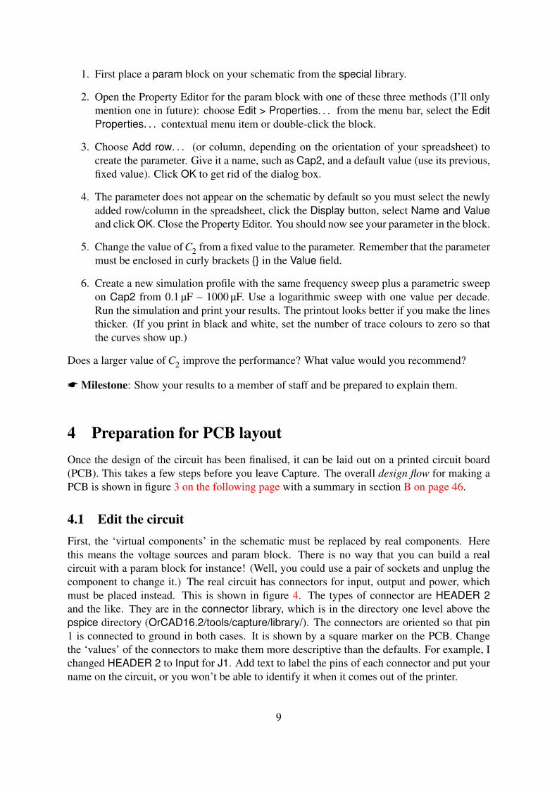
I mentioned above that we use a local library of footprints rather than those supplied with PCBEditor and must therefore tell the applications where to find our library. You should only haveto do this once.
1. Choose Setup > User Preferences. . . from the menu bar, which brings up the UserPreferences Editor.
2. Expand Paths in the list of Categories and choose the Library folder.
3. First change psmpath, where PCB Editor looks for package symbols (footprints). Clickon the Value button, which shows only ‘. . . ’, to bring up a box entitled psmpath Items.
4. Click the New (Insert) button (the leftmost one), which adds an empty item to the listwith another ‘. . . ’ button. Click this button, which brings up the usual Windows SelectDirectory box.
5. Navigate to the Elecapps drive (Q), find the allegro directory, then pcb_lib and finallysymbols. Click OK to select this directory.
6. Next we must tell PCB Editor to look in our local directory before the default libraries,denoted by $psmpath. Click on $psmpath followed by the Move Down arrow. Thepsmpath Items box should now look like figure 6 on the next page except that yourdirectories are different (my computer is not on the same network). Click OK.
13
Figure 6. Completed dialogue box for setting up psmpath. Your directory path is different.
7. Follow the same procedure for padpath, which uses the padstacks directory withinpcb_lib. This is the information for the padstacks, the copper islands used for mount-ing components, including holes for pin-through-hole components.
8. Click OK to dismiss the User Preferences Editor.
Define the board
Choose File > New. . . from the menu. In the first dialogue box, set the Drawing Type toBoard (wizard). Click Browse. . . , navigate to your new allegro directory and give the board aname such as bare.brd. Click Open then OK to bring up the new board wizard. This takes youthrough several screens to define the parameters of the PCB. Some of these are obvious, suchas the size of the board, while others set up the design rules – the width of tracks on the PCB,how much space must be left between them, and so on.
1. The first screen is purely descriptive. Read it, then click Next >.
2. This asks for a board template. We don’t have one so select No (probably the default)and click Next >.
3. You are next asked for a ‘tech’ file. This is short for a technology file, which specifies thedesign rules – number of layers, widths and separation of tracks and so on. We won’t useone for this design so select No and click Next >.
4. This asks for a board symbol. We don’t have one so select No again and click Next >.
5. We now reach the screens for the parameters that must be set up. The units shouldbe Mils. These are not millimeters but the American term for thousandths of an inch;1mm≈ 40mils. All dimensions are given in these units so get used to them.
14

Leave the drawing size at A. This is an American size but you aren’t allowed EuropeanA4 if the units are mils. Leave the origin at the centre.
6. Set the grid spacing to be 100 mils.
The Etch layer count is the number of copper layers on the board – the number of layersof tracks for signals and power. Leave this at 2, although we shall use only one layer inthe first design.
Don’t worry about the artwork films – we don’t use them.
7. Leave the names of the layers as Top and Bottom and their types as Routing Layer.
8. Enter 25 for the Minimum Line width (in mils). This value will propagate into the otherboxes. It means 0.025′′ or about 0.64 mm, which is very wide for a track nowadays butmakes the board easy to produce and solder by hand.
For the Default via padstack, click on the button with . . . and choose GU-VIA80. Thisdesign is far too simple to need vias, which carry a signal from one layer of the PCB toanother, but they may be required in future projects.
9. Rectangular board (it’s curious that a circular board is the default).
10. Enter a width of 3000 and height of 2000 mils. This defines the board outline as 3′′×2′′.There is no corner cutoff.
Specify the Route keepin distance as 100. A keepin means that objects must be keptinside the specified region. In this case it means that tracks cannot go any closer than100 mils to the edge of the board. It gives a border around the PCB to aid handling andmanufacture. (We’ll encounter keepouts as well later.)
Set the Package keepin distance to 250. Components must be placed within this keepinand therefore cannot be closer than 250 mils to the edge of the board. The gap betweenthe two keepins allows you to run tracks around the outside of all the components, whichis often helpful on a more complicated board.
11. Click Finish – that’s it.
This has set up the design rules and made an empty board, which you can see in the mainwindow of PCB Editor, shown in figure 8 on page 18. Three rectangles are visible for the boardoutline, route keepin and package keepin. Choose File > Save and close PCB Editor.
The next step is to return to Capture and send the circuit to PCB Editor so that it can beadded to the bare board.
4.5 Create a netlistThe information about your design is sent from Capture to PCB Editor in the form of a netlist,which contains a description of the circuit and its components. (The netlist comprises threefiles but you don’t need to look at them.)
1. Highlight your design (the object whose name ends in .dsn) in the Project Managerwindow of Capture.
15

Figure 7. Completed dialogue box for netlisting the design and sending it to PCB Editor. Yourfile names will be different.
2. Select Tools > Create Netlist. . . from the menu bar, which brings up a dialogue box asin figure 7. Make sure that the PCB Editor tab is active.
3. Check that the PCB Footprint box contains PCB Footprint.
4. Check that the box underneath for Create PCB Editor Netlist is selected.
5. Under Options, the Netlist Files Directory should be shown as allegro. Select Create orUpdate PCB Editor Board (Netrev).
6. For Input Board File, choose the bare board that you have just set up. Click on the ‘. . . ’button to navigate.
7. The Output Board File usually shows something sensible automatically; edit it if not. Itshould use the new allegro directory.
8. Under Board Launching Option, select Open Board in OrCAD PCB Editor because ourlicence doesn’t cover the full version of Allegro.
9. The entries in the dialogue box should now resemble figure 7 except for the pathnames.Click OK to dismiss this dialog box and start the netlister.
16

You are warned that your design will be saved by Capture, then a Progress box shows thevarious processes needed: Netlisting the design followed by Updating OrCAD PCB EditorBoard. PCB Editor is then launched with your new board.
• A Warning box tells you that Netrev succeeded with warnings. Check the Session Logif this happens. Messages about RVMAX and CMAX can be ignored; these are maximumvoltage ratings of the components and are not important for this circuit. Pay attention toany others and seek advice if they are unclear.
• OrCAD PCB Editor gives you a warning that Database was last saved by a higher tiertool, which you can ignore.
You should now see your empty board outline on the screen of PCB Editor again; the compo-nents are invisible at this stage.
5 OrCAD PCB EditorOrCAD PCB Editor is the basic version of the Allegro PCB Editor from Cadence. Despitebeing ‘basic’ it is vastly more powerful than is needed for the simple designs that we shalllay out in this course. Its interface may feel unfamiliar because the application was originallydeveloped for unix and has been ported to Windows with minimal changes. Some distinctivefeatures are obvious almost immediately.
• The design window, which shows your board, has no scroll bars.
• One design is always open; you cannot open more than one, nor close the current designwithout opening a new one or exiting the application.
• There is no ‘null’ tool, such as the pointer shown by most drawing applications when noother tool is selected.
An important aspect of the interface is that tools can be used in two ways.
• First choose a command, either from the menu bar or by clicking a button, then theelement of the design on which the tool should operate.
• Select the object first, then the command from the contextual menu by right-clicking.
I shall use both methods in the tutorials, picking whichever seems most natural at the time.However, confusion can arise when you change from one method to the other. It is therefore agood idea when switching to disable any active tool (right-click and choose Done if it is offered)and clear any selection (left-click outside the board or right-click and choose Selection Set >Clear All Selections).
5.1 The screenPCB Editor needs a big screen – the elderly laptop that I have used to illustrate these instructionsis not large enough to show all the toolbars! The main elements of the application are shown infigure 8 on the next page.
17

Figure 8. Screenshot of OrCAD PCB Editor with an empty board. The rectangles show theboard outline (outer), route keepin and package keepin (inner). The control panels have col-lapsed to tabs on the right and the background of the windows has been changed to white for aclearer printout.
• Design window, occupying most of the screen, where you lay out the PCB. It alwaysshows the board viewed from the top; the bottom layer is seen through the board as if itwere transparent.
• Menu bar along the top as usual.
• Toolbars in two rows under the menu bar and a further column down the left-hand side.Their arrangement depends on the size of the screen. Hover the pointer over a button toreveal its function.
• Control panels with tabs on the right-hand side. Each panel pops out when you movethe pointer over its tab. Click the pin to lock a panel open.
– Find selects the type of object that is highlighted when you move the mouse aroundthe drawing.
– Options changes according to the current mode and command; it selects the activeclass and subclass when PCB Editor is idle, then offers appropriate options when acommand is chosen.
18

– Visibility hides layers of etch while routing the board.
Pin the Find and Options panels open if your screen is large enough; Visibility is lessuseful in boards with only one or two layers of etch.
• Command console window at the bottom left of the screen. This prints a running logof your actions and is useful to show when Allegro is waiting for input from you. It alsodisplays the output from commands such as Design Rules Check.
• Worldview window at bottom right shows how the relation between the board outlineand the view in the main design window. It is useful for moving the design windowaround the board as we shall soon see.
• Status bar at the bottom of the screen. It shows the coordinates of the pointer (crosshairs).The P (Pick) button is useful for typing coordinates instead of clicking with the mouse ifyour hand is unsteady.
At the far right is a coloured block called DRC, which stands for Design Rules Check (asyou remember from Capture, of course). It may be yellow because checking is not up todate. Usually it should be green to show that automatic checking is turned on and that noerrors are detected.
A lot of jargon is associated with Allegro. It often refers to your design as the database, becausethat’s what it is from the point of view of the computer. The various elements of the designare classified into classes and subclasses, which I’ll write as class/subclass in the instructions.Here are some common examples.
• The Etch class includes the regions of copper that act as pads for the components andthe tracks that carry the signals between them. Our designs have two subclasses of etch,Top and Bottom. They are coloured green and yellow respectively.
• The Board Geometry class includes the Outline, which we have already seen. Sub-classes Silkscreen_Bottom and Silkscreen_Top are used for text to annotate the board.
• We have also seen the Package Keepin class, used to prevent components being placedtoo close to the edge of the board. It has no subclasses.
The active class and subclass can be chosen in the Options control panel but PCB Editor usuallyselects them automatically when you make a tool active.
5.2 Moving around the designTwo methods can be used to pan or roam around the design – move the display to the region ofinterest.
• Use the arrow keys on the keyboard.
• Hold down the middle button of the mouse and drag. A confusing feature of this is thatit drags the window over the design. This means that the design moves in the oppositedirection to your drag. It is the reverse of the hand ‘grabber’ in applications such asAcrobat, which drag the design under the window.
19
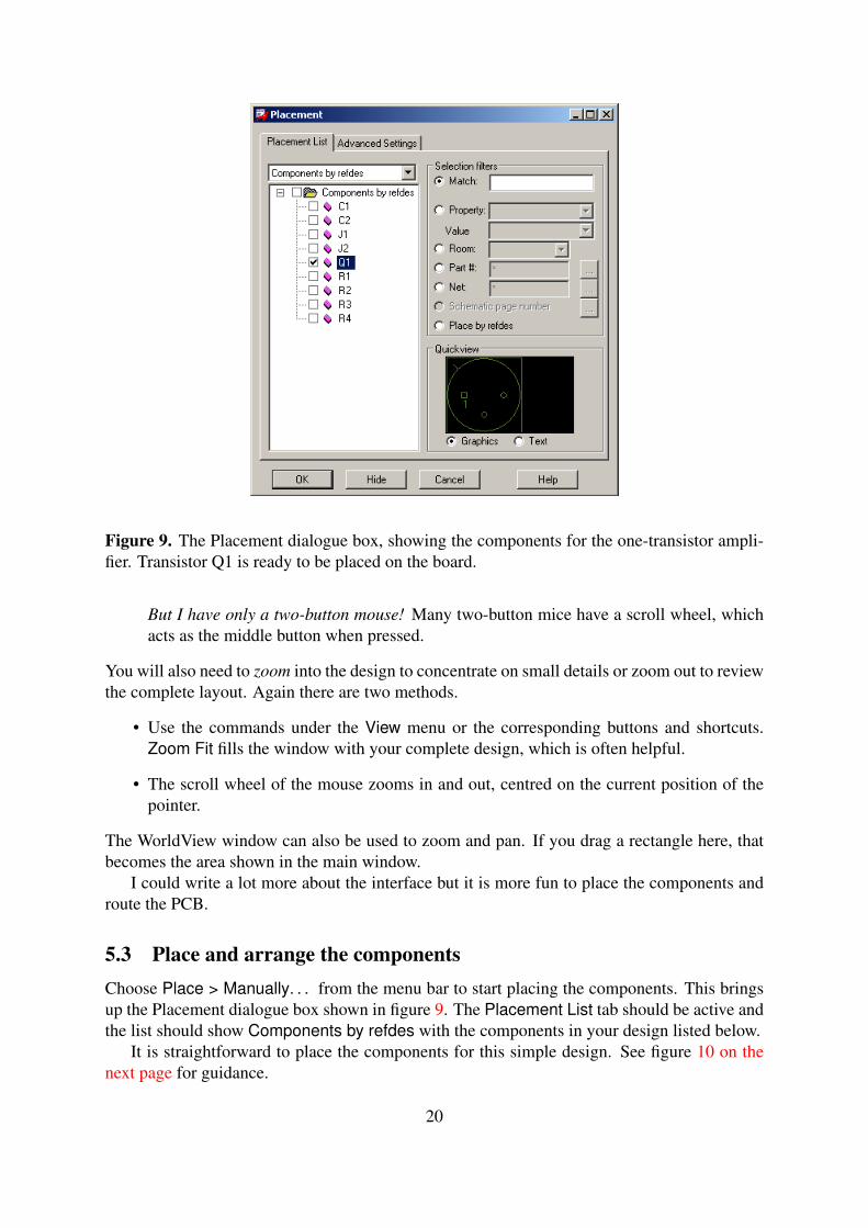
Figure 9. The Placement dialogue box, showing the components for the one-transistor ampli-fier. Transistor Q1 is ready to be placed on the board.
But I have only a two-button mouse! Many two-button mice have a scroll wheel, whichacts as the middle button when pressed.
You will also need to zoom into the design to concentrate on small details or zoom out to reviewthe complete layout. Again there are two methods.
• Use the commands under the View menu or the corresponding buttons and shortcuts.Zoom Fit fills the window with your complete design, which is often helpful.
• The scroll wheel of the mouse zooms in and out, centred on the current position of thepointer.
The WorldView window can also be used to zoom and pan. If you drag a rectangle here, thatbecomes the area shown in the main window.
I could write a lot more about the interface but it is more fun to place the components androute the PCB.
5.3 Place and arrange the componentsChoose Place > Manually. . . from the menu bar to start placing the components. This bringsup the Placement dialogue box shown in figure 9. The Placement List tab should be active andthe list should show Components by refdes with the components in your design listed below.
It is straightforward to place the components for this simple design. See figure 10 on thenext page for guidance.
20

Figure 10. Screenshot of the board for the simple, one-transistor amplifier after all compo-nents have been placed and arranged. Cyan lines of the ratsnest show the connections betweencomponents.
1. Start with the transistor. Click the box next to Q1 in the Placement dialogue. Its outlineappears in the Quickview box.
2. Move the cursor out of the Placement box on to your design. The outline of the transistoris attached to the cursor. Left-click to place it centrally on your board. The outline willbe filled in and a small P for ‘placed’ appears in the Placement box next to the refdes.
3. Place the connectors for input and output next. Select the boxes for both J1 and J2.Move the mouse onto the design and a two-pin header for J1 appears on the cursor. Clicksomewhere near the left-hand side to place it. Don’t worry about its orientation for now.
4. The outline of J2 now appears automatically on the cursor; place this on the right-handside.
5. Next place the four resistors. Put them in the same positions relative to the transistor thatthey have on your schematic drawing. This makes the circuit easier to wire. Refer toyour schematic drawing to identify each resistor.
Keep all components inside the inner purple rectangle, which shows the Package Keepin.It turns green if you try to place any part of a component outside it.
6. Place the two capacitors in the same way. This completes the placement so dismiss thedialogue box.
The components are joined by a set of cyan lines called the ratsnest to show their logicalconnections. These lines will be turned into copper tracks when you route the board. The linesof the ratsnest simply take the shortest path between components and therefore cross otherlines. Real tracks cannot do this. It is therefore vital to adjust the orientation and position of theplaced components to reduce the number of crossings in the ratsnest and make routing easier.
Before doing this, experiment by moving the mouse around the design window withoutclicking. Elements of the design are highlighted and an explanatory note appears as the mouse
21
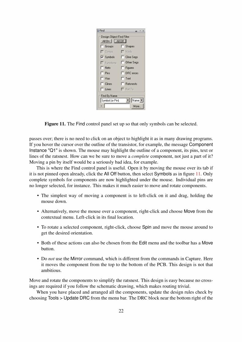
Figure 11. The Find control panel set up so that only symbols can be selected.
passes over; there is no need to click on an object to highlight it as in many drawing programs.If you hover the cursor over the outline of the transistor, for example, the message ComponentInstance "Q1" is shown. The mouse may highlight the outline of a component, its pins, text orlines of the ratsnest. How can we be sure to move a complete component, not just a part of it?Moving a pin by itself would be a seriously bad idea, for example.
This is where the Find control panel is useful. Open it by moving the mouse over its tab ifit is not pinned open already, click the All Off button, then select Symbols as in figure 11. Onlycomplete symbols for components are now highlighted under the mouse. Individual pins areno longer selected, for instance. This makes it much easier to move and rotate components.
• The simplest way of moving a component is to left-click on it and drag, holding themouse down.
• Alternatively, move the mouse over a component, right-click and choose Move from thecontextual menu. Left-click in its final location.
• To rotate a selected component, right-click, choose Spin and move the mouse around toget the desired orientation.
• Both of these actions can also be chosen from the Edit menu and the toolbar has a Movebutton.
• Do not use the Mirror command, which is different from the commands in Capture. Hereit moves the component from the top to the bottom of the PCB. This design is not thatambitious.
Move and rotate the components to simplify the ratsnest. This design is easy because no cross-ings are required if you follow the schematic drawing, which makes routing trivial.
When you have placed and arranged all the components, update the design rules check bychoosing Tools > Update DRC from the menu bar. The DRC block near the bottom right of the
22

Figure 12. Screenshot of the routed board for the simple, one-transistor amplifier. The tracksare yellow, which shows that they are on the bottom of the board. Your screen may not matchthis image exactly because it depends on which classes are active at the time.
window turns green and the Command window shows No DRC errors detected if everythingis correct. If you have placed a component outside the keepin, for example, the message wouldbe DRC done; 1 errors detected. The error is shown by a tiny red ‘butterfly’ marker on thedesign. Move the component inside the keepin and the marker disappears.
Save your design with a new name for the populated board. Unusually, Allegro asks youif you wish to overwrite an existing file when you Save it. You may wish to save successiveversions under different names in case you need to go back and repeat a step. Allegro does notsave backups automatically.
5.4 Route the boardThe electrical connections depicted by the ratsnest must now be replaced by copper tracks onthe PCB. This procedure is called routing the board. The layers of copper are called etch inAllegro because of the usual manufacturing process. Tracks should be drawn on the bottomof the board with the components on the top (where they go by default). The wires from thecomponents pass through the holes in the pads and are soldered to the tracks on the bottom ofthe board.
Jargon: cline is short for connecting line, a segment of a copper track. A plain line may showthe edge of the board or the outline of a component and is not a conductor. ¦
Keep the layout of tracks as straightforward as possible – imagine that you are solderingthe board yourself. Do not make life difficult by running tracks unnecessarily close to pads, forinstance. You should aim for something like the layout shown in figure 12 but there is no needto follow this precisely.
Draw the tracks as follows. Before starting, check that no objects are selected (left-clickoutside the board or right-click and choose Selection Set > Clear All Selections) and that no
23

(a) (b) (c)
Figure 13. (a) Options and (b) Find control panels for the Add Connect command, and (c) Op-tions for Slide.
tool is active (right-click and choose Done if it is offered). Pin the Find and Options controlpanels open, which makes it easier to control the tools.
1. Choose Route > Connect from the menu bar.
2. The Options control panel changes to reflect the current activity and it now shows thelayers available for routing. We want all the tracks to go on the bottom of the board sochange the Act (active) layer to Bottom, which is painted yellow. You can also changethe Alt (alternate) layer to Top, which is painted green, but we need only one layer forthis circuit. Line lock should be 45 (degrees), which determines the allowed change indirection of a track. See figure 13(a).
The Find control panel (figure 13(b)) is automatically configured to select the relevantobjects for routing: pins, vias, shapes, cline segments and ratsnests. (Shapes are typicallyareas of etch, which is why they are active.)
3. Left-click on a pin to start routing a segment – the part of a track that runs from one pinto another. A segment of the ratsnest highlights to show that it is available for routing.
4. Move the mouse towards the pin at the other end of the highlighted ratsnest. A thickyellow line is drawn to show the copper track and replaces the line of the ratsnest.
5. Click at intermediate points to fix corners. These automatically turn through 45°, whichis good practice. It is a bad idea to draw 90° corners because they are prone to breakageduring etching.
6. Click on the destination pin to complete the track.
7. Repeat to route all segments of the ratsnest. Right-click and choose Done when you havefinished.
24

Run a design rules check to detect any problems with routing. For further details, chooseDisplay > Status. . . from the menu bar. The section on Symbols and nets should show thateverything has been placed and routed, while DRC errors should be shown as Up To Date withno errors. Save your board.
Oops! – I made a mistake
There are several ways of undoing an error.
• Right-click the mouse and choose Oops. This undoes the most recent partial action, suchas drawing the last segment of a track.
• Right-click and choose Cancel, which undoes the last complete action.
• Try Edit > Undo to go further back.
• If you have made a complete mess, go to the menu File > Recent Designs and reloadyour design without saving changes (there is no Revert to Saved command). This aban-dons all changes since you last saved the file, which I hope was not too long ago. . . .
My tracks don’t look very good: How can I improve them?
PCB Editor offers many ways of adjusting the tracks. First make sure that you are not still usingthe Connect tool by right-clicking and choosing Done if this appears on the contextual menu.Small adjustments to routed tracks can be made with the Route > Slide tool, which loads theOptions control panel as shown in figure 13(c) on the previous page. I suggest that you changeBubble from its default of Shove preferred, because this encourages Allegro to move tracksaround in a startling manner; Hug only is more gentle. Click and release the mouse button on asegment to select it, slide it around and click again when you are satisfied with the result. Otherhelpful tools include Edit >Vertex and Edit > Delete Vertex.
For larger changes, you might wish to remove part of a track or the complete track andredraw it. Proceed as follows.
• Move the mouse over a cline segment, which should highlight. If it does not, open theFind control panel and choose All On.
• You can delete the etch at three levels using the contextual menu:
– Delete removes the segment – a single straight line of track between corners orpins.
– Connect Line > Delete removes the complete track (cline) between the two nearestpins or junctions.
– Net > Ripup etch unroutes the complete net.
• Use Route > Connect to redraw the track.
This nicely illustrates the way in which PCB Editor allows a hierarchy of selections: just asegment, a complete line, or the whole net.
25

Aaarghh! – I’ve just spotted an error in the circuit
If you spot an error in the circuit, rather than the layout, follow the instructions in section Aon page 45. You can correct the schematic drawing in Capture and send a new netlist to PCBEditor, which makes only the minimum number of alterations to your board. It is not necessaryto repeat the whole layout. This is one of the advantages of computer-aided design.
5.5 Add textNext add some text to the board to make it easier to fabricate and use. In particular, all con-nectors (headers) must have the function of each pin identified as on the schematic. Your namewould be useful too. There is no need to add a label for each component because the refdes andvalue are shown automatically. Text and the outlines of components are printed on a commer-cial board using ink or paint as a layer called the silkscreen. We cannot produce a silkscreen inthe department and text must therefore be placed on the copper layers.
1. Start by putting your name on the board, which is always a good idea if you want to claimit. Choose Add > Text from the menu.
2. Use the Options control panel to select the destination for the text. You are probablygetting the hang of the interface by now: choose a command, select options, then do it.
• Put essential text such as your name on the bottom layer of copper because this ispart of every board. The Active Class should therefore be Etch and the Subclassshould be Bottom.
• Text on the bottom of the board should be mirrored so that it reads correctly frombelow, so select the Mirror box.
• Text block is a confusing way of specifying the size of text. A larger number for theblock produces larger text. Something like 4 is about right for your name.
3. Click in the design where you would like the text and type. Hit Return (Enter) to get anew line. Click to begin a new block of text elsewhere or right-click and choose Donewhen you have finished.
4. Now add some text on top of the board to identify the connectors. Again choose Add >Text but this time set the active class and subclass to Etch/Top. Turn off the mirroringand reduce the size to 2.
Add text for Input and Ground near the input connector and Power, Output and Groundby the output connector. Keep the text away from the pads: It is printed in copper andcould cause a short circuit.
Congratulations! – you have finished your first PCB. Don’t forget to save it.
5.6 Print the designThe simplest way of printing the design is to ‘plot’ it (the usage goes back to the days of penplotters). Select File > Plot Setup. . . from the menu and choose the following settings.
26

• Usually the Plot scaling should be unity so that the size of the printout matches that ofthe PCB. This board is so simple that it is better to enlarge the drawing so enter 2 instead.
• Change the Default line weight to 10, otherwise the outlines are thin and indistinct.
• Set the Plot method to Color and close the dialogue box.
Open the Options control panel and set the active class to Etch/Bottom. This emphasizes themost important features. Now print your layout with File > Plot. . . .
• Click on the Setup. . . button and check that the paper is in landscape orientation.
• Adjust the Print quality if necessary (probably not).
Check the output with the PDF printer first to save printer credits. The result should resemblefigure 12 on page 23. Print the final image on paper using the colour printer, whose price hasbeen reduced for this class, and stick the output in your laboratory record book.
This plot is not useful for manufacturing the PCB. In the next design I’ll show you how toget printouts that can be used to make your PCB in the department.
* Milestone: Ask a member of staff to assess your finished design.
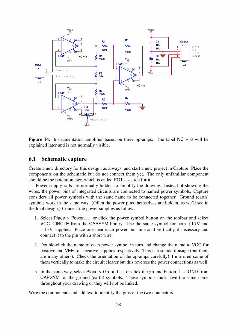
6 Instrumentation amplifier – single-sided boardThe second design is another classic circuit, shown in figure 14 on the following page. This isan instrumentation amplifier based on three op-amps. You will study its operation in AnalogueElectronics 2. Its main characteristics are as follows.
• Both inputs have a high input resistance because each is connected directly to the non-inverting input of an op-amp.
• The third op-amp acts as a subtracter to pick out the difference between its inputs (it canprovide gain as well but I have chosen not to do this).
• The gain for differential signals (the difference V+−V−) can be adjusted with the singleresistor R2.
• The gain for common-mode signals (where V+ = V−) is very low.
The circuit is used to amplify a small difference in voltage between its two inputs while reject-ing a large background or noise voltage that affects the two inputs equally. This is often neededwith sensors, so remember this in Team Design Project 3. It may also be helpful later this year.
In practice it is unlikely that the circuit would be built using three separate packages withsingle op-amps as in this design. Complete instrumentation amplifiers are available in 8-pinpackages. Even if these were unsuitable, a quad package that contains four op-amps could beused although these lack the pins for trimming the offset voltage. We shall not simulate thiscircuit, just lay out the PCB. The LF411 is a widely used op-amp.
27
VCC
VEE
VEE
VCC
VEE
VCC
VEE
VCC
VEE
Inverting
Non-inverting
+15 V
0 V
-15 V
Output
Offset null
J2
Output
J2
Output
1234
U2
LF411
NC = 8U2
LF411
NC = 8
+3
-2
V+
7V
-4
OUT6
B11
B25
R7
100k
R7
100k
R6
100k
R6
100k
C1
10u
16V
C1
10u
16V
R5
100k
R5
100k
R4
100k
R4
100k
J1
Input
J1
Input
12
R8
10K
SET = 0.5
R8
10K
SET = 0.5
R3100kR3100k
C2
10u
16V
C2
10u
16V
R210kR210k
R1100kR1100k
U1
LF411 NC = 8
U1
LF411 NC = 8
+3
-2
V+
7V
-4
OUT6
B11
B25
U3
LF411
NC = 8U3
LF411
NC = 8
+3
-2
V+
7V
-4
OUT6
B11
B25
Figure 14. Instrumentation amplifier based on three op-amps. The label NC = 8 will beexplained later and is not normally visible.
6.1 Schematic captureCreate a new directory for this design, as always, and start a new project in Capture. Place thecomponents on the schematic but do not connect them yet. The only unfamiliar componentshould be the potentiometer, which is called POT – search for it.
Power supply rails are normally hidden to simplify the drawing. Instead of showing thewires, the power pins of integrated circuits are connected to named power symbols. Captureconsiders all power symbols with the same name to be connected together. Ground (earth)symbols work in the same way. (Often the power pins themselves are hidden, as we’ll see inthe final design.) Connect the power supplies as follows.
1. Select Place > Power. . . or click the power symbol button on the toolbar and selectVCC_CIRCLE from the CAPSYM library. Use the same symbol for both +15V and−15V supplies. Place one near each power pin, mirror it vertically if necessary andconnect it to the pin with a short wire.
2. Double-click the name of each power symbol in turn and change the name to VCC forpositive and VEE for negative supplies respectively. This is a standard usage (but thereare many others). Check the orientation of the op-amps carefully! I mirrored some ofthem vertically to make the circuit clearer but this reverses the power connections as well.
3. In the same way, select Place > Ground. . . or click the ground button. Use GND fromCAPSYM for the ground (earth) symbols. These symbols must have the same namethroughout your drawing or they will not be linked.
Wire the components and add text to identify the pins of the two connectors.
28

Two of the op-amps have unconnected pins. These pins are intentionally unused becausethey are for offset adjustment and it is only necessary to do this on one op-amp. PCB Editormust be told about this, otherwise it assumes that you omitted the connections by mistakeand flags an error. Show that the pins are deliberately unconnected by choosing Place > NoConnect from the menu bar or clicking the appropriate button, then clicking on the pins. Asmall cross appears as in figure 14 on the previous page. PCB Editor requires every pin to beconnected or explicitly marked as not connected.
Run a Design Rules Check and correct any errors. Next enter the footprints. I’m not givingyou a table this time: You must work out which to use. A catalogue of our local library isshown at the end of this handout and the components themselves are available in the laboratoryso that you can match them up.
Fixup. Incompatibilities between Capture and PCB Editor must again be corrected beforemaking the netlist. First, the pins of the electrolytic capacitors are wrongly numbered. Repeatthe instructions in section 4.1 on page 9 to fix this. ¦
Fixup. A new problem is that only 7 pins are defined on the electrical symbols for the op-ampsbut the package has 8 pins. You might hope that the software would assume that undefined pinsare not connected but it does not: It must be told this formally.
1. Select one of the op-amps and choose Edit > Part, which brings up the Part Editor.
2. Choose Options > Part Properties. . . , which brings up the list of User Properties.
3. Click the New. . . button. Give the new property the name NC, which stands for No Con-nect, and the value 8, which is the number of the unconnected pin. (Use a list separatedby commas, such as 7,8, if more pins are not connected.)
4. Click OK to get rid of the dialog boxes and close the Part Editor. Choose Update All sothat this change is applied to all LF411 parts in your design.
I have made the NC property visible on the schematic in figure 14 on the previous page, whichtherefore shows NC = 8, but you need not do this. ¦
Print your schematic when it has been completed correctly and survived the DRC.
* Milestone: Have your drawing checked before you go any further.
6.2 Create the PCB and place the componentsRemember to make an allegro directory first. Set up the board as before (section 4.4 on page 13)but make it 3.5′′×2.5′′, which gives you plenty of room for the larger number of components.Save the board and quit from PCB Editor. Back in Capture, create a netlist and send the designto PCB Editor as before. Check the Session Log: Ignore any warnings about RVMAX butinvestigate any others.
We’ll place the components using a different technique this time. Choose Place > Quick-place. . . from the menu bar. The defaults should be suitable (Place all components, Around
29

Figure 15. Constraint manager after changing the widths of the three power nets but beforecorrecting the vias. The widths should be 50 and 25, not 30 and 20 as shown here.
package keepin, Top). Click Place then OK. Your components are now arranged at the top ofthe board, ready for you to move them into position.
Move the components onto the board, arrange them to resemble the schematic drawing andadjust them to make the ratsnest simple with as few crossings as possible (it is not possible toeliminate all of the crossings). This step is really important. It is easy to route the tracks ona well-placed board; conversely, a poorly-placed board needs long, convoluted tracks or mayeven be unroutable.
Run a Design Rules Check when the components have all been placed and save your board.
6.3 Add mounting holesMost PCBs need to be mounted inside a piece of equipment and therefore need holes for fixings.Mounting holes and similar features are called mechanical symbols and are placed in a slightlydifferent way from electronic components because they are not part of the netlist.
1. Select Place > Manually. . . to open the Placement dialogue box, bring the AdvancedSettings tab forward and choose to Display definitions from Library. This is necessarybecause the symbols are not in the database imported from Capture.
2. Return to the Placement List tab and select Mechanical symbols from the drop-down list.
3. Use the same procedure as before to place a GU-MOUNTING156 symbol near eachcorner of the board. This is a hole of diameter 156 mils or 5
32′′. Do not place the holes
too close to the edge or the board may break when it is drilled.
Mounting holes are shown on my routed PCB in figure 20 on page 35.
30
6.4 Preparation for routingPower tracks are usually made wider than signal tracks because they have to carry more current.Our tracks are already so wide that it’s barely necessary but we’ll do it for future reference.
1. Choose Setup > Constraints > Physical. . . from the menu bar. This brings up theConstraint Manager and a Tip of the Day if you are unlucky (sigh).
2. The left-hand part of the window shows the various properties that can be edited. Clickon All Layers under Net. See figure 15 on the preceding page for guidance.
3. The main part of the window now shows a list of the nets in your design. Most of themhave random-looking numbers, such as N00451, but a few are named. These are thenets that carry power, to which we assigned names in Capture: VCC, VEE and GND orsomething similar, depending on the symbol that you chose.
4. Change the minimum width for these three nets from 25 to 50 mil.
5. Choose File > Close to return to PCB Editor.
Save a copy of your board before routing so that you can use it for double-sided routing.
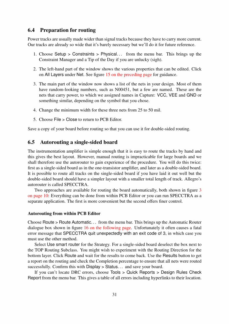
6.5 Autorouting a single-sided boardThe instrumentation amplifier is simple enough that it is easy to route the tracks by hand andthis gives the best layout. However, manual routing is impracticable for large boards and weshall therefore use the autorouter to gain experience of the procedure. You will do this twice:first as a single-sided board as in the one-transistor amplifier, and later as a double-sided board.It is possible to route all tracks on the single-sided board if you have laid it out well but thedouble-sided board should have a simpler layout with a smaller total length of track. Allegro’sautorouter is called SPECCTRA.
Two approaches are available for routing the board automatically, both shown in figure 3on page 10: Everything can be done from within PCB Editor or you can run SPECCTRA as aseparate application. The first is more convenient but the second offers finer control.
Autorouting from within PCB Editor
Choose Route > Route Automatic. . . from the menu bar. This brings up the Automatic Routerdialogue box shown in figure 16 on the following page. Unfortunately it often causes a fatalerror message that SPECCTRA quit unexpectedly with an exit code of 3, in which case youmust use the other method.
Select Use smart router for the Strategy. For a single-sided board deselect the box next tothe TOP Routing Subclass. You might wish to experiment with the Routing Direction for thebottom layer. Click Route and wait for the results to come back. Use the Results button to geta report on the routing and check the Completion percentage to ensure that all nets were routedsuccessfully. Confirm this with Display > Status. . . and save your board.
If you can’t locate DRC errors, choose Tools > Quick Reports > Design Rules CheckReport from the menu bar. This gives a table of all errors including hyperlinks to their location.
31

Figure 16. Dialog box for running the autorouter from within PCB Editor.
After all tracks have been successfully routed, choose Route > Gloss. . . from the menubar. Glossing means to tidy up the design. This includes spreading tracks apart where possibleand replacing 90° corners by 45° bends (mitering). Accept the defaults and gloss your design.Finally, use Tools > Quick Reports > Etch Length by Layer Report to find the lengths of thetracks and add them up. In general, a better design has shorter tracks.
Autorouting with SPECCTRA
Use the manual equivalent of the flow described in the previous section if automatic routingdoes not work from PCB Editor. It’s a bit clumsier but gives better control over the process andmakes it easier to experiment with different settings.
Note. At some point you may get a Licensing Error warning from SPECCTRA. Click IgnoreFeature for This Session if it appears. ¦
1. Choose File > Export > Router from the menu bar of PCB Editor. It asks you for aname for the Auto-Router Design file and you can probably accept the suggestion. ClickRun. You may be warned about overwriting the file, which isn’t a problem. A messageTranslation Completed should appear, after which you can close the box.
32

Figure 17. Startup dialogue box for importing a design into SPECCTRA.
Figure 18. Screenshot of SPECCTRA, ready to route the instrumentation amplifier. I havechanged the background of the window to white for a clearer printout.
33

Figure 19. Settings in the Layers box for single-sided routing on the bottom layer anddouble-sided routing on both layers.
2. Start SPECCTRA for OrCAD from the Windows Start menu. You are presented withthe fairly complicated dialogue box shown in figure 17 on the previous page. Use theBrowse. . . buttons to open the following two files.
• For the Design / Session File (the first), choose the file that you just exported fromPCB Editor.
• For the Do File (the last), choose the file with _rules appended to the name of yourboard file.
Click Start Allegro PCB Router to dismiss the box. SPECCTRA starts and you shouldnow see your components joined by the ratsnest within the outline of the route keepin asin figure 18 on the preceding page. Some components have shaded footprints, which I’llexplain later.
3. Tell SPECCTRA to route only the bottom layer. Choose View > Layers. . . from themenu bar. Turn routing off for the top layer by clicking on the drop-down menu next toTOP as shown in figure 19 and selecting the � symbol. You might like to experimentwith the setting of the BOTTOM layer. The directions are hints to the router but inpractice tracks will be drawn in both directions. Click Close when you have finished.
4. Choose Autoroute > Route. . . . Leave Smart selected and click OK. The autorouterwill work away and you will see Message: Smart_route finished, completion rate:100.00% if all is well. The tracks should be in colour, yellow for the bottom, if they arerouted successfully. Sometimes they are drawn white, which should indicate a designrules error, even when they appear to be correct – I don’t know why.
See the suggestions below if the autorouter is unable to route your board.
5. Two further commands improve the tracks for assembly. First choose Autoroute > PostRoute > Spread Wires. . . and accept the defaults. This spreads the tracks away fromeach other and from the solder pads.
6. You’ll have noticed that the autorouted board has 90° bends in the tracks, which I toldyou to avoid when you routed the board by hand. We’ll now sort this out. Run Autoroute> Post Route > [Un]Miter Corners. . . and accept the defaults. The corners will berounded off and tracks run diagonally where possible.
34

Figure 20. My one-sided layout after autorouting. The total routed length was 29.3′′.
7. To see the details of the finished layout, choose Report > Route Status. This will show alot more than you want to know! Look near the bottom and confirm that the Unconnectedlength is zero. Record the Routed length in your notebook.
8. Choose File > Quit. . . and agree to Save and Quit. This writes a session file thatdescribes the routed tracks.
9. Return to PCB Editor and choose File > Import > Router. . . . Locate the Session Filewhose name matches your board and click Run. You should see a message TranslationCompleted. Close the box.
10. The window now shows your design with tracks instead of the ratsnest. Save it under adifferent name to preserve the unrouted board for later.
Help! – My board won’t route
Here are some suggestions for helping the autorouter.
1. If routing has almost worked (only one or two unrouted segments), try changing the hintsgiven to the router. For the one-sided board there is only the suggested direction of tracks.It is best to unroute the board and begin afresh. Choose Edit > Delete Wires > All Wiresfrom the menu bar of SPECCTRA or reload the unrouted version of your board in PCBEditor.
2. If you are far from success, look at the layout to see where the problems lie. Often oneparticular track prevents successful routing. Can you rearrange the components to solvethe problem?
35

Figure 21. Part of the Color Dialog box, showing the settings for the Stack-Up to plot thebottom layer.
Quit from SPECCTRA without saving, or reload the previous version of your board inPCB Editor. Rearrange or reorientate components to make the ratsnest simpler and easethe problem before trying the autorouter again.
If none of this works, get advice from a demonstrator.
6.6 Final touchesAdd text on the top etch layer to identify all pins on the connectors and put your name on thebottom etch layer as before. Run a final design rule check, save your routed board and makea coloured plot as before. My layout is shown in figure 20 on the preceding page. It is a poorboard in many respects despite the successful routing. The power tracks are excessively long inparticular. It is not hard to see how the components could be rearranged to improve the layout.
6.7 PhotomaskThis section explains how to get a black-and-white plot that can be used as a photomask tomanufacture your board in this department. I’m afraid that the procedure is complicated be-cause Allegro is not intended for such a primitive process. A further difficulty is that we needholes in the pads to guide the drill. The general idea is to hide unwanted elements of the designand colour the desired features black. Save your design first.
1. Open the Color Dialog box with Display > Color/Visibility. . . from the menu bar.
2. Click the button to turn Global Visibility Off, agree to Make all classes invisible in thesmall dialogue and click Apply in the main dialogue (this is needed after every change tosee the effect). The design vanishes from the design window.
3. Click the Display folder in the list on the left. We must change the Background colourof the window so that tracks show up after their colour has been changed to black. Clickon the white swatch in the Color swatches (samples of each colour) near the bottom ofthe window, then click the swatch next to Background, which turns white. Click Applyto update the design window, which also turns white.
36

Figure 22. Printout at actual size for manufacturing a single-sided board (bottom layer) withholes in the pads to guide the drill.
4. Now we need make the desired features visible again and paint them black. Start byselecting Board Geometry from the list on the left. This brings up a set of Subclasses tothe right. Select the checkbox next to Outline to turn it on. Change its colour to black byclicking in the black swatch in the Color region, then the swatch next to Outline. Finally,click Apply and the board outline becomes visible in the design window.
5. This must be repeated for all the features that we wish to print. For the bottom of a PCBthese are Stack-Up/Conductor/Bottom/Pin, Via and Etch. Activate and make them blackas shown in figure 21 on the previous page. Click Apply and your tracks appear.
6. Finally we must make the drill holes white. They are normally hidden in a layer calledthe filmmask, which must be made visible. Click All for Filmmaskbottom to activate itand change its colour to white. Click OK to close the Color Dialog.
7. The holes do not yet appear on the screen because they are ‘under’ the etch. Go to theOptions control panel and choose the Pin/Filmmaskbottom class, which makes it activeand draws it on top of everything else. Pale holes appear on the pads as desired. Thiscompletes the bottom of the PCB.
8. Check the Plot Setup. Set the Scaling factor to 1.00 so that the mask has the correctdimensions for the finished PCB. Leave the Default line weight as 10 or text may be toothin for reliable etching.
9. Finally, choose File > Plot. . . as usual and you should get a beautiful picture with theboard outline and etch as in figure 22.
After all this, quit from PCB Editor without saving (or reload your design) to avoid messing upthe colours next time you use it.
* Milestone: Ask a member of staff to assess your design.
37
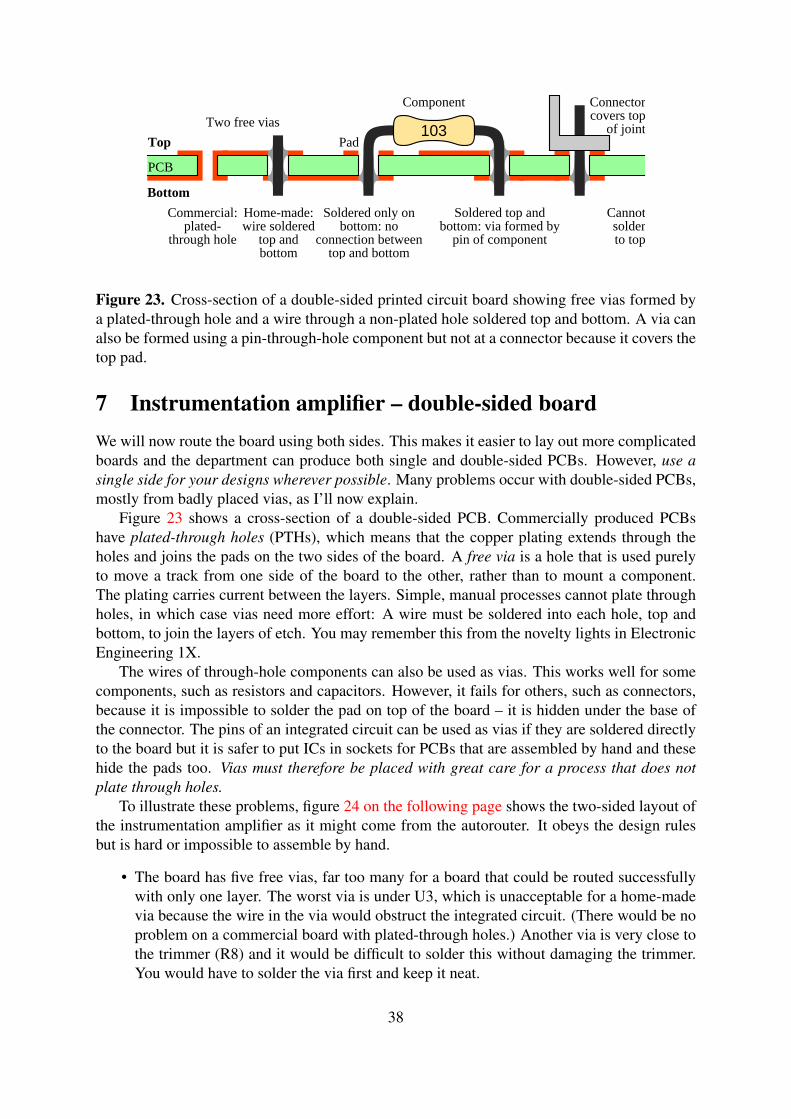
103
PCB
Pad
Component
Commercial: plated-
through hole
Top
Bottom
Two free vias
Connectorcovers top
of joint
Home-made: wire soldered
top and bottom
Soldered top and bottom: via formed by
pin of component
Soldered only on bottom: no
connection between top and bottom
Cannot solderto top
Figure 23. Cross-section of a double-sided printed circuit board showing free vias formed bya plated-through hole and a wire through a non-plated hole soldered top and bottom. A via canalso be formed using a pin-through-hole component but not at a connector because it covers thetop pad.
7 Instrumentation amplifier – double-sided boardWe will now route the board using both sides. This makes it easier to lay out more complicatedboards and the department can produce both single and double-sided PCBs. However, use asingle side for your designs wherever possible. Many problems occur with double-sided PCBs,mostly from badly placed vias, as I’ll now explain.
Figure 23 shows a cross-section of a double-sided PCB. Commercially produced PCBshave plated-through holes (PTHs), which means that the copper plating extends through theholes and joins the pads on the two sides of the board. A free via is a hole that is used purelyto move a track from one side of the board to the other, rather than to mount a component.The plating carries current between the layers. Simple, manual processes cannot plate throughholes, in which case vias need more effort: A wire must be soldered into each hole, top andbottom, to join the layers of etch. You may remember this from the novelty lights in ElectronicEngineering 1X.
The wires of through-hole components can also be used as vias. This works well for somecomponents, such as resistors and capacitors. However, it fails for others, such as connectors,because it is impossible to solder the pad on top of the board – it is hidden under the base ofthe connector. The pins of an integrated circuit can be used as vias if they are soldered directlyto the board but it is safer to put ICs in sockets for PCBs that are assembled by hand and thesehide the pads too. Vias must therefore be placed with great care for a process that does notplate through holes.
To illustrate these problems, figure 24 on the following page shows the two-sided layout ofthe instrumentation amplifier as it might come from the autorouter. It obeys the design rulesbut is hard or impossible to assemble by hand.
• The board has five free vias, far too many for a board that could be routed successfullywith only one layer. The worst via is under U3, which is unacceptable for a home-madevia because the wire in the via would obstruct the integrated circuit. (There would be noproblem on a commercial board with plated-through holes.) Another via is very close tothe trimmer (R8) and it would be difficult to solder this without damaging the trimmer.You would have to solder the via first and keep it neat.
38

Figure 24. Screenshot of a poor double-sided layout with several badly-placed vias.
• Several pins of resistors act as vias – R3 has two, for instance. These are easy.
• The pins of the integrated circuits are connected to tracks on both the top and bottom.This is not a problem if the IC is soldered directly to the board but won’t work if it is ina socket.
• The connectors (J1 and J2) and the trimmer (R8) have tracks only to the bottom of theirpins. This is why the via is needed near R8. No tracks run to the top because the symbolsfor these components have route keepouts on the top, which forbid the router from placingtracks there. The footprints have diagonal shading in SPECCTRA to show this, visiblein figure 18 on page 33.
The general rule is to avoid vias wherever possible. Every via requires two soldered joints (topand bottom), which dramatically reduces reliability.
Now route your board for the instrumentation amplifier using both sides.
1. Re-open the unrouted version of your board.
2. Remember the Default via padstack when you used the new board wizard? We specifiedGU-VIA80. Unfortunately there seems to be a bug with this because another type of viacalled simply VIA appears in the design and is used wrongly by default. The problem isthat VIA is much too small to be soldered by hand so we must get rid of it.
Fixup. Choose Setup > Constraints > Physical. . . from the menu bar. Select PhysicalConstraint Set > All Layers to bring up the spreadsheet shown in figure 15 on page 30.The column headed Vias for the DEFAULT row probably has VIA:GU-VIA80. Highlightthis cell and choose Edit > Change. . . . Remove VIA from the Via list on the right and
39

click OK. The cell now contains only GU-VIA80, which is what we want. Close theConstraint Manager and save your board. ¦
3. Run the autorouter from within PCB Editor or export the board to SPECCTRA as before.This time you should allow routing on both layers, which is the default. You might liketo experiment with the directions. Note the routed length and the number of vias; a gooddesign may have none at all, which is a bonus. Remember to gloss or space and mitre thetracks.
4. Import the tracks into PCB Editor if you used SPECCTRA . Save the routed board undera new name.
You must move any vias in inconvenient places, such as that under U3 in figure 24 on theprevious page. If you are lucky you may be able to Slide the via but it is often better to rip upthe complete track and re-route it by hand. Other tracks must often be moved to create spacefor the via.
• Select the cline or net with the offending via, right-click and choose Delete or Ripupetch from the contextual menu.
• Select the connect tool and check in the Options control panel that the active and alternatelayers are correct.
• Draw out the segments of the track as usual.
• Double-click when you reach the point where a via is needed. A via is inserted androuting switches to the alternate layer.
• Continue routing to complete the track.
I made several changes to my board to get the final version in figure 25 on the following page.
• The via was moved from under U3 to a clear region of PCB.
• Another via was moved away from R8.
• The via near C1 was eliminated by rerouting the tracks slightly.
• Several tracks were moved from the top to the bottom, which makes the board easier tosolder by hand.
• It would have been better to edit the board further so that all tracks leave the ICs on thebottom of the board. This would require extensive rerouting and more vias to be inserted.I also prefer to avoid vias in the tracks for power and ground.
It is best to install ICs in sockets for projects but it is a nuisance to stop the autorouter runningtracks to the top pads, where they are inaccessible. We have therefore provided alternativefootprints, such as GU-DIPSOCK8 instead of GU-DIP8, with route keepouts on the top thatforce all tracks to use the bottom pads.
When you have finished editing the board, add text to both layers of etch to identify them.Finally, plot the finished board in colour.
* Milestone: Ask a member of staff to assess your finished design.
40

Figure 25. Double-sided layout after improving the layout and moving the badly-placed vias.
Photomasks for double-sided boards
Separate masks for the top and bottom layers are required for production but you can omit thisstep now. For future reference you should follow the instructions in section 6.7 on page 36 forthe bottom and repeat the process with two small changes for the top photomask.
1. Activate and colour the top subclasses instead of the bottom subclasses.
2. Open Plot Setup and choose Mirror under Plot orientation.
The top plot must be mirrored because the printed side of the mask is turned over and placednext to the copper when the photoresist is exposed. A good check is that text should be mirroredon both masks for a double-sided board. (The text on the bottom is also mirrored on yourcomputer’s screen but the text on the top is mirrored only on the plot.)
8 A mixed-signal systemThe final design is a mixed-signal system. This means that it includes both analogue and digitalcomponents like the project in this course. In fact this design is one approach to the projectin 2007–08, which was an electronic weight scale. We used the MC9S08GB60 on a SofTecdemonstration board and the display module from Embedded Processors 2. The project was todesign and build the electronics required between the sensor and the microcontroller. Figure 26on the following page shows the circuit. These are its principal features.
• An instrumentation amplifier (again), which amplifies the small signal from the weightsensor. It includes adjustments for the gain and offset voltage.
41

SC
LK
nSS
MIS
O
MIS
OS
CLK
nSS
PTE
6P
TE7
PTE
6P
TE7
VC
C
VC
C
VC
C
VC
C
VC
CV
+
R7
100k
R7
100k
R8
47k
R8
47k
U1D
LM32
4
U1D
LM32
4
+12
-13
V+4
V-11
OU
T14
SW
1
Tare
SW
1
Tare
R9
10k
R9
10k
C1
100n
C1
100n
J1Sen
sor
J1Sen
sor
1234
R10
10k
SE
T =
0.5
R10
10k
SE
T =
0.5
U1B
LM32
4
U1B
LM32
4
+5
-6
V+4
V-11
OU
T7
SW
2
Cal
ibra
te
SW
2
Cal
ibra
teC
210
0nC
210
0n
U1C
LM32
4
U1C
LM32
4
+10
-9
V+4
V-11
OU
T8
C3
10u
16VC3
10u
16V
R1
100k
R1
100k
R2
4.7k
R2
4.7k
R3
100k
R3
100k
R4
100k
R4
100k
U1A
LM32
4
U1A
LM32
4
+3
-2
V+4
V-11
OU
T1
U2
TLC
549
U2
TLC
549
AIN
2
I/OC
LK7
RE
F+1
RE
F-3
DO
UT
6
CS
5
J2
Sof
tecJ2
Sof
tec
2 4 6 8 10 12 14 16
1 3 5 7 9 11 13 15
R11
4.7k
R11
4.7k
R5
100k
R5
100k
R6
100k
R6
100k
Figu
re26
.Ins
trum
enta
tion
ampl
ifier
and
anal
ogue
-to-
digi
talc
onve
rter
fora
nel
ectr
onic
wei
ghts
cale
.
42

• The output of the instrumentation amplifier enters an analogue-to-digital converter (ADC,part TLC549), which converts the analogue voltage to a digital value.
• The digital value is transferred to a GB60 microcontroller on a Softec board througha serial peripheral interface (SPI). Its signals are called MISO, MOSI (not used here),SCLK and CS; the last is active low so I called it nSS on the diagram.
• Two pushbuttons Tare (set to zero) and Calibrate the system. They are connected togeneral-purpose input/output (GPIO) pins of the microcontroller.
A 4-way Molex connector is required for the weight sensor and a 8×2 header (just two rowsof pins) for a ribbon cable to the SofTec board. Several new aspects of standard practice areillustrated on this schematic drawing.
• The four op-amps are in a single package, LM324, called a quad op-amp. This is whythey have the letters A–D at the end of their refdes. Capture automatically uses successiveop-amps in a multiple package until it runs out and needs a further package. The inputsand output of each op-amp have distinct pins but the power pins are the same for all four.
• The variable resistor R11 is a ‘virtual component’ (you will not find one in stores). Re-place this by a real (variable) component.
• Many connections are made by name rather than drawing lines, using a net alias.
1. Draw a short wire on the appropriate pins.
2. Choose Place > Net Alias. . . from the menu bar or use the button on the toolbar.
3. Enter the name for the Alias and click OK.
4. Click on the wire(s) that you wish to name.
• Although the power pins of the op-amp are shown (they are often hidden completely),they are not attached to wires. Instead they are connected purely by name. A powersymbol with the same name as the power pin of the op-amp must be connected to theappropriate supply rail. This is V+ for the positive supply.
Add a further power symbol named V− and connect it to ground. The shape of the symboldoesn’t matter, just its name. This connects the negative supply of all the op-amps toground. (The op-amps are used in a single supply configuration, where their negativesupply pin is connected to ground rather than a negative voltage.)
• The power pins of the ADC aren’t shown at all (REF+ and REF− are reference voltagesrather than power.) Find the names of the pins by opening the Property Editor and makingthe Pins sheet active. Add power symbols with these names to the supplies to provide thecorrect connections. Do not wire the pins themselves.
• The three capacitors in parallel are for decoupling noise and must be positioned carefullywhen you lay out the PCB. One of the 100 nF capacitors should be as close as possibleto the power pins of the op-amp and the other should be close to those of the ADC. Theplacement of the 10 µF electrolytic capacitor is less critical.
43

• The pushbuttons are in a local Capture library called EDP2LIB. Download this from themoodle page and copy it to your project folder for this design.
Four pins are needed on the symbol, although only two seem necessary, because thephysical pushbutton has four pins and the schematic must match this.
• Note the orientation of the 8×2 header carefully. Pin 1 is top left when viewed from thetop of the board but the part is mirrored in some libraries.
* Milestone: Ask a member of staff to check your schematic drawing before proceeding.
Here are a few tips to help you lay out the PCB.
• Aim to keep the noisy, digital SPI away from the sensitive analogue inputs.
• The four op-amps within the LM324 are identical so you might wish to swap them aroundto improve the layout – I assigned the four randomly.
• Make the power and ground tracks wider as usual.
• Select footprints using the components available in the laboratory.
• Mark pin 1 of the 8× 2 header clearly on the top of the board to show which way thecable should be plugged in. The ribbon cable has a red stripe to identify pin 1.
Most of the design should work as before but you may encounter a puzzling new feature ofPCB Editor: the nets for VCC and ground do not appear in the ratsnest. The reason is thatseparate planes in the PCB are often used for power and ground, in which case there is no pointin showing the connections – they are made directly to the planes. PCB Editor therefore hidespower nets by default. This isn’t useful for our single and double-sided boards so make the netsvisible as follows.
1. Choose Edit > Net Properties. . . to bring up the Constraint Manager, then Net andGeneral Properties.
2. There is a column headed No Rat and the entry is probably On in the rows for VCC andGND. Change these entries to (Clear), which should empty the cells.
3. Quit from the Constraint Manager and the nets should appear in the ratsnest. Seek expertadvice if they remain invisible.
* Milestone: Ask a member of staff to assess your finished design. Congratulations! ReadMitzner’s book [1] if you would like to learn more about PCB Editor.
44

References[1] Kraig Mitzner, Complete PCB Design using OrCAD Capture and PCB Editor, Newnes
(Elsevier), 2009, ISBN 9780750689717, about £40. Read this book if you wish to learnmore about PCB Designer. Highly recommended. Mitzner covers many features that arenot explained in these notes and explains the background theory, which I barely touch.The only disadvantage is that Mitzner concentrates on practice for commercial boards,reasonably enough, but we have to follow a slightly different process for boards made inthe department.
[2] Clive Maxfield, Bebop to the Boolean Boogie: An unconventional guide to electronics,3rd edition, Newnes, 2009, ISBN 9781856175074. You might not guess from its title butthis includes a wide-ranging description of modern components and construction includingPCBs. An entertaining read.
[3] David L Jones, PCB Design Tutorial, www.alternatezone.com. This is a good, practicalguide to the design and manufacture of PCBs but not specific to OrCAD. The commentson CAD software are a little out of date but it is full of real-world advice.
A How to correct a layout if you spot an error in the circuitIt would be highly irritating if you had to repeat the whole layout after making a change to acircuit. The good news is that it is surprisingly easy to make corrections and that you alreadyknow the steps.
1. Save your board in its current state and quit from PCB Editor.
2. Re-open Capture and make the corrections to your circuit. Always run a DRC beforeproceeding.
3. Repeat the instructions in section 4.5 on page 15 for creating a netlist and sending it toPCB Editor with these small changes.
• For Input Board File, choose the board that you just saved in PCB Editor – the mostrecent version of your layout.
• Use a distinct name for the Output Board File to create a new board.
4. The new board opens in PCB Editor with the minimum number of changes to accom-modate the revisions to your circuit. You will have to place any extra components andre-route any tracks that were disturbed.
The jargon for this process is that Capture sends an Engineering Change Order (ECO) to PCBEditor.
45

B Summary: PCB design flowThis checklist is adapted from a handout by Mr I. Young. Save your work frequently!
1. Make a new directory for each design. Create an allegro directory within it.
2. Start Capture, create a new project in the new directory and draw the circuit.
• Select an Analog or Mixed A/D project if you wish to simulate the circuit. Alterna-tively, try the PC Board Wizard, which gives you the choice of simulation or notand offers appropriate libraries.
• Use libraries in the pspice directory if you wish to simulate your design. If not,you may prefer libraries in the library directory, one level higher. (For example,you could take passive components from library/discrete rather than library/pspice/analog.) These cause fewer warnings from the netlister.
• A helpful, local library of symbols is available in Q/TDP3_ORCAD/Projects.olb.
• Use wires to join components, symbols and junctions – don’t just push them to-gether.
• Provide power connections for all integrated circuits. If power pins are hidden youmust place power symbols with matching names on the supply rails.
• Include a connector for power from a battery or power supply.
• Check the circuit carefully before starting the layout: It is much easier to correctmistakes now. If you spot an error in the circuit later, refer to section A.
3. Prepare the schematic for PCB Editor.
• Edit components with incorrectly numbered pins, such as the electrolytic capacitorin the analog library.
• Mark all unconnected pins with the No Connect symbol.
• Add the No Connect property NC to packages with pins that are not shown on thesymbol in Capture (for example, pin 8 of single op-amps in DIP8 packages).
• Add footprints from our local library, prefix GU-. The catalogue is in the directoryQ/allegro/pcb_lib/. In most cases you should use the dipsock footprints rather thandip for integrated circuits to prevent tracks running to the top pads.
• Run a Design Rules Check. Check the Session Log even if no warning dialoguebox is shown and correct any errors. Print the final schematic to guide the layout.
4. Create a bare board in PCB Editor using the New Board Wizard.
• Set up the search paths if necessary. Add Q/allegro/pcb_lib/symbols to psmpathand similarly for padpath.
• Use 25 mil design rules so that your board will be easy to etch and solder.
• Make the size of board generous; you can reduce it later.
• Choose GU-VIA80 for the default via.
46

5. Netlist the design in Capture. Check all warnings in the the Session Log carefully evenif PCB Editor appears to be launched successfully.
6. Place the components on the board in PCB Editor. Pin the Find and Options panels opento control the operation of the tools.
• Take time to arrange and orient the components to simplify the ratsnest as far aspossible. This step is critical to get a well-routed board.
• Add mounting holes if required. Do not place them too close to the edge.
• Use Setup > Constraints > Physical. . . to increase the width of tracks for thepower supplies and other tracks that carry a heavy current.
• Also fix the list of vias so that only GU-VIA80 is shown.
• Run a Design Rules Check and correct any errors.
7. Route the board.
• Manual routing is best for a simple design (which includes most of ours).
• If you must use the autorouter, try a single-sided board first. Use Display > Sta-tus. . . to check that the completion rate is 100%.
• If only a few tracks are not routed automatically, complete them by hand and putvias in convenient places. Use wires on top instead of a double-sided board.
• If you must use a double-sided board, review the results of the autorouter carefully.Move any vias and tracks to pads on the top that cannot be soldered easily.
• Gloss the design in PCB Editor or SPECCTRA.
8. Add text on the etch layer(s) to identify the board and connectors.
9. Write photomasks as pdf files at actual size. Follow the instructions carefully and re-member to select a filmmask in the Options control panel so that guide holes appear inthe pads.
10. Take your board (.brd) and pdf files to Mr I. Young in the SPEED group (room 512A).He will check the layout and print the photomasks.
11. Take the photomasks to Mr S. Fairbairn in the electronics workshop (room 712A). Hewill etch and drill your PCB. Finished boards are left in pigeonholes in the electronicsstores, just outside the workshop and data library.
Mr Young is always happy to assist students with PCB design. Please feel free to ask him ifyou need a footprint for a component that is not in the library or if you encounter problems thatare not solved by this handout.
This handout is available on moodle under General Information > Laboratories, which youcan enter as a guest. A further handout describes more advanced techniques in PCB Editor,which you may wish to explore. For example, it explains how to add a copper ‘pour’ to a PCBas a ground plane and how to create footprints (package symbols).
47