C2000 Digital Power BoosterPack - TI.com · The C2000 Digital Power BoosterPack provides a quick...
34
TI Designs C2000™ Digital Power BoosterPack TI Designs Design Features TI Designs provide the foundation that you need • Features a Non-Isolated, Digitally-Controlled DC- including methodology, testing and design files to DC Buck Converter quickly evaluate and customize the system. TI Designs • Offers a Quick and Easy Way to Learn About help you accelerate your time to market. Digital Power Supply Control Using C2000™ MCUs • Offers an Onboard Active Load for Transient Design Resources Performance Testing Tool Folder Containing Design Files TIDM-DC-DC-BUCK • Offers Various powerSUITE Tools – Compensation Designer – Software Frequency Response Analyzer ASK Our E2E Experts (SFRA) WEBENCH® Calculator Tools – Solution Adapter Featured Applications • Server Power Supplies • Telecom Rectifiers • Industrial Power Supplies • UPS Systems • Smart Grid and Energy • Automotive Charging • Data Storage An IMPORTANT NOTICE at the end of this TI reference design addresses authorized use, intellectual property matters and other important disclaimers and information. C2000, Texas Instruments, LaunchPad, Code Composer Studio, controlSUITE, NexFET are trademarks of Texas Instruments. All other trademarks are the property of their respective owners. 1 TIDU986 – September 2015 C2000™ Digital Power BoosterPack Submit Documentation Feedback Copyright © 2015, Texas Instruments Incorporated
Transcript of C2000 Digital Power BoosterPack - TI.com · The C2000 Digital Power BoosterPack provides a quick...

TI DesignsC2000™ Digital Power BoosterPack
TI Designs Design FeaturesTI Designs provide the foundation that you need • Features a Non-Isolated, Digitally-Controlled DC-including methodology, testing and design files to DC Buck Converterquickly evaluate and customize the system. TI Designs • Offers a Quick and Easy Way to Learn Abouthelp you accelerate your time to market. Digital Power Supply Control Using C2000™ MCUs
• Offers an Onboard Active Load for TransientDesign ResourcesPerformance Testing
Tool Folder Containing Design FilesTIDM-DC-DC-BUCK • Offers Various powerSUITE Tools– Compensation Designer– Software Frequency Response AnalyzerASK Our E2E Experts (SFRA)WEBENCH® Calculator Tools– Solution Adapter
Featured Applications• Server Power Supplies• Telecom Rectifiers• Industrial Power Supplies• UPS Systems• Smart Grid and Energy• Automotive Charging• Data Storage
An IMPORTANT NOTICE at the end of this TI reference design addresses authorized use, intellectual property matters and otherimportant disclaimers and information.
C2000, Texas Instruments, LaunchPad, Code Composer Studio, controlSUITE, NexFET are trademarks of Texas Instruments.All other trademarks are the property of their respective owners.
1TIDU986–September 2015 C2000™ Digital Power BoosterPackSubmit Documentation Feedback
Copyright © 2015, Texas Instruments Incorporated
TIDU986–September 2015
IntroductionThe C2000 Digital Power BoosterPack provides a quick and easy way to learn about digital power supplycontrol and design using C2000 MCUs. This board consists of a DC-DC synchronous buck power stagecontrolled by a TMS320F28069M LaunchPad™ (LAUNCHXL-F28069M not included). The softwareaccompanying this design at www.ti.com/controlsuite allows programming the controller andexperimenting with control parameters to tune the control loop for optimal system performance. Anonboard active load allows transient performance testing. This kit supports powerSUITE tools including thecompensation designer, software frequency response analyzer, and solution adapter. The software projectlets you evaluate the complete system with the help of these tools. This reference design shows how toconnect a buck converter power stage to a C2000 digital power controller
This guide presents how to use this board and the accompanying software with the powerSUITE tools.This guide offers a structured, step-by-step method that starts with simple open-loop excitation andproceeds to a complete, well-tuned, closed-loop system.
3TIDU986–September 2015 IntroductionSubmit Documentation Feedback
Copyright © 2015, Texas Instruments Incorporated
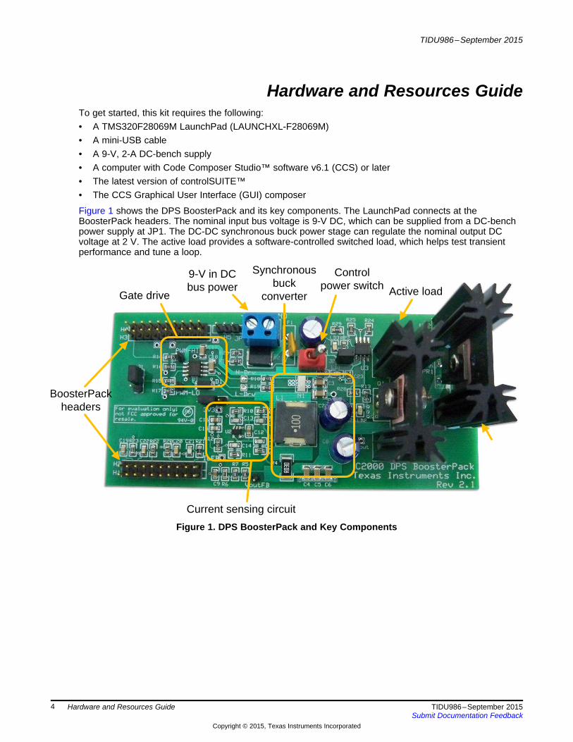
Gate drive
9-V in DC bus power
Synchronous buck
converter Active load
Current sensing circuit
BoosterPack headers
Control power switch
TIDU986–September 2015
Hardware and Resources GuideTo get started, this kit requires the following:• A TMS320F28069M LaunchPad (LAUNCHXL-F28069M)• A mini-USB cable• A 9-V, 2-A DC-bench supply• A computer with Code Composer Studio™ software v6.1 (CCS) or later• The latest version of controlSUITE™• The CCS Graphical User Interface (GUI) composer
Figure 1 shows the DPS BoosterPack and its key components. The LaunchPad connects at theBoosterPack headers. The nominal input bus voltage is 9-V DC, which can be supplied from a DC-benchpower supply at JP1. The DC-DC synchronous buck power stage can regulate the nominal output DCvoltage at 2 V. The active load provides a software-controlled switched load, which helps test transientperformance and tune a loop.
Figure 1. DPS BoosterPack and Key Components
4 Hardware and Resources Guide TIDU986–September 2015Submit Documentation Feedback
Copyright © 2015, Texas Instruments Incorporated
www.ti.com
Table 1. Key Components
Component Description9 V In (JP1) Vin - DC-power supply (Minimum 8.5 V, Maximum 12 V)BoosterPack Headers LaunchPad interface
SW1 - Power switch to connect or disconnect the DC bus to or fromControl Power Switch Vin.Buck Converter Synchronous buck power stage (includes TI NexFET™ Power Block)Load 7.5-Ω resistive load permanently connected across the outputActive Load Software-controlled switched load (2 Ω)
Buffered PWM drive to ensure quick and efficient turn on or off of theGate Drive power FETsInductor current feedback for current monitoring andCurrent Sensing overcurrent protection
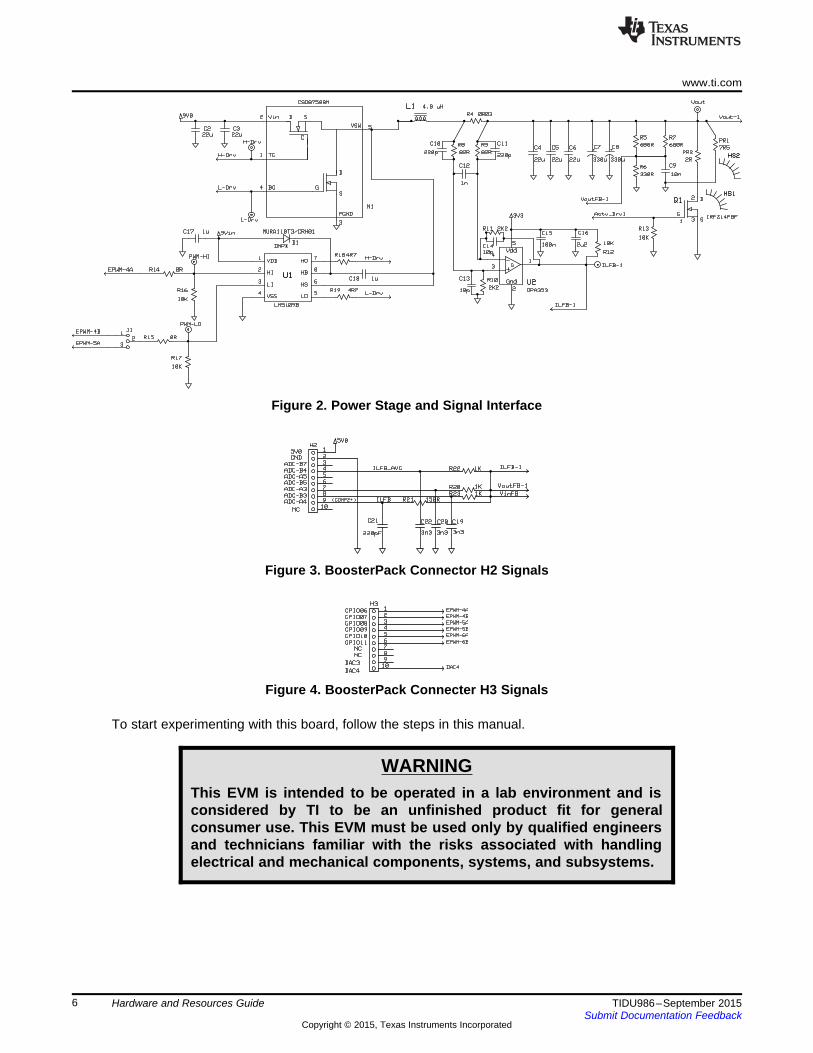
The TMS320F28069M microcontroller on the F28069M LaunchPad controls the synchronous buckoperation by driving the high-side and low-side switches of the NexFET power block N1 using on-chipPWM signals. Sense resistor R4 and op-amp U2 sense, condition, and feed the current through theinductor L1 back to the MCU. This synchronous buck power stage operates at a 200-kHz switchingfrequency. A low-load PR1 is permanently connected between the synchronous buck output and ground.A high-load PR2 can be switched in and out of the circuit using the MOSFET switch Q1 by driving Q1 witha 50% duty cycle PWM signal. This capability provides an active load feature at run time and allowstransient performance tests and tuning. PR2 can also be turned on continuously to increase output loadwhich causes the inductor current to stay positive and nonzero, and providing better loop responsemeasurements.
Table 2 lists the key signal connections between the F28069M LaunchPad and the DPS BoosterPack. Fora portion of the schematic, see Figure 2.
Table 2. Key Signal Connections
Signal Name Description Connection to LaunchPadEPWM-4A High-side drive signal for synchronous buck (PWM-HI) GPIO-06EPWM-4B Low-side drive signal for synchronous buck (PWM-LO) GPIO-07EPWM-5A Alternate low side drive signal (PWM-LO) GPIO-08EPWM-6A PWM duty control signal for active load GPIO-10VoutFB-1 Output voltage feedback ADC-A3ILFB Inductor current feedback (overcurrent protection) ADC-A4ILFB_AVG Inductor current feedback (heavily filtered) ADC-B4VinFB Input voltage feedback ADC-B3
5TIDU986–September 2015 Hardware and Resources GuideSubmit Documentation Feedback
Copyright © 2015, Texas Instruments Incorporated
www.ti.com
Figure 2. Power Stage and Signal Interface
Figure 3. BoosterPack Connector H2 Signals
Figure 4. BoosterPack Connecter H3 Signals
To start experimenting with this board, follow the steps in this manual.
WARNINGThis EVM is intended to be operated in a lab environment and isconsidered by TI to be an unfinished product fit for generalconsumer use. This EVM must be used only by qualified engineersand technicians familiar with the risks associated with handlingelectrical and mechanical components, systems, and subsystems.
6 Hardware and Resources Guide TIDU986–September 2015Submit Documentation Feedback
Copyright © 2015, Texas Instruments Incorporated
Timer 2 tasks:InstrumentationSFRA_Background
Main
Background loop
Background loop
Initialization28x Device levelPeripheral level
System levelSFRA initISR, ADC
Timer 1 tasks:Trip level adjustSlew limitManage active load
Timer 3 tasks:Fault managementOther tasks
ISR
SFRA_inject()
DPL_func()
SFRA_collect()
Exit
C Environment
DPL_Func()
SFRA_inject()
TIDU986–September 2015
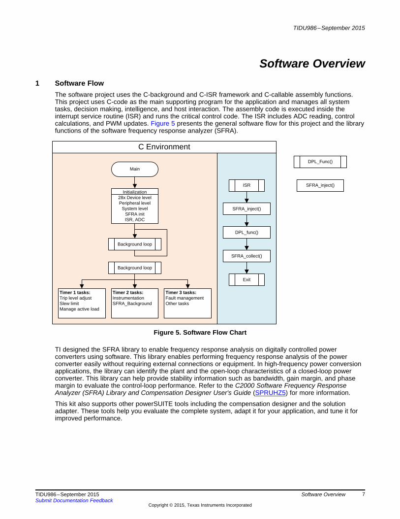
Software Overview1 Software Flow
The software project uses the C-background and C-ISR framework and C-callable assembly functions.This project uses C-code as the main supporting program for the application and manages all systemtasks, decision making, intelligence, and host interaction. The assembly code is executed inside theinterrupt service routine (ISR) and runs the critical control code. The ISR includes ADC reading, controlcalculations, and PWM updates. Figure 5 presents the general software flow for this project and the libraryfunctions of the software frequency response analyzer (SFRA).
Figure 5. Software Flow Chart
TI designed the SFRA library to enable frequency response analysis on digitally controlled powerconverters using software. This library enables performing frequency response analysis of the powerconverter easily without requiring external connections or equipment. In high-frequency power conversionapplications, the library can identify the plant and the open-loop characteristics of a closed-loop powerconverter. This library can help provide stability information such as bandwidth, gain margin, and phasemargin to evaluate the control-loop performance. Refer to the C2000 Software Frequency ResponseAnalyzer (SFRA) Library and Compensation Designer User's Guide (SPRUHZ5) for more information.
This kit also supports other powerSUITE tools including the compensation designer and the solutionadapter. These tools help you evaluate the complete system, adapt it for your application, and tune it forimproved performance.
7TIDU986–September 2015 Software OverviewSubmit Documentation Feedback
Copyright © 2015, Texas Instruments Incorporated

Software Flow www.ti.com
Figure 6 shows an overview of the typical process flow for designing and tuning a system using thepowerSUITE tools.
Figure 6. Designing and Tuning a System Process Flow Chart
The solution adapter lets you adapt code examples from TI digital power supply kits and configure them torun on your custom digital power supply board using the same topology and similar resources. The GUIguides you through the process of selecting the solution to adapt, selecting the relevant options for thatsolution, and customizing those options to adapt the software solution to your hardware design.
The compensation designer is a software utility that helps power engineers design multiple digitalcompensators that achieve the closed-loop performance of a closed-loop control system they desire. Youcan achieve this performance using the measured power stage or plant data from the SFRA tool or usingthe modeled power stage as part of the solution adapter. The solution adapter generates the coefficientsthat require programming on the device and can be copied into the code directly. The default project usesa 2-pole 2-zero control law and does not support 3-pole 3-zero compensators.
The key framework C files in this project are the following:• Buck_VMC-Main.c – This file initializes, runs, and manages the application.• Buck_VMC-DevInit_F2806x.c – This file initializes and configures the microcontroller once. This one-
time initialization and configuration includes setting up the clocks, PLL, GPIO, and so forth.• Buck_VMC-DPL.asm – This file contains all time, critical control-type code in a C-callable assembly
function and has an initialization section and a runtime function from the ISR.
The digital power library modules are called from this framework.
8 Software Overview TIDU986–September 2015Submit Documentation Feedback
Copyright © 2015, Texas Instruments Incorporated

Duty1AOutRef
Fdbk
CNTL_2P2Z:1:
Coef
B0B1B2A1A2
DminDmax
CNTL_2P2Z_CoefStruct
DBUFF
ADC
ADCDRV_1ch:1:
ADCDRV_1ch_Rlt VoutFB-1Adc_Vout1
Adc_Vout1
Vout_Ref_wInjDuty1A
PWMnA
PWMnB
PW
M
PWMDRV_1ch:n:
Duty
Period
www.ti.com Software Flow
Library modules may have both a C and an assembly component. Table 3 lists the C configure functions,their initialization macros, and runtime macros.
Table 3. Library Modules
C Configure Function ASM Initialization Macro ASM Runtime MacroPWM_1ch_UpCntDB_ActivHIC_Cnf. PWMDRV_1ch_INIT n PWMDRV_1ch ncADC_SOC_Cnf.c ADCDRV_1ch_INIT n ADCDRV_1ch n
CNTL_2P2Z_INIT n CNTL_2P2Z n
Figure 7 shows the control blocks.
Figure 7. Control Blocks
The dark teal blocks represent hardware modules on the C2000 microcontroller. Light blue blocks are thesoftware drivers for these modules. The yellow block is the controller block for the control loop. Although a2-pole 2-zero controller is used in this design, you can use a PIPID, a 3-pole 3-zero, or any othercontroller that can be implemented for this application. This modular library structure lets you convenientlyvisualize and understand the complete system software flow and easily use and add or delete functions.By implementing an incremental build approach, this project demonstrates the these functions.
9TIDU986–September 2015 Software OverviewSubmit Documentation Feedback
Copyright © 2015, Texas Instruments Incorporated

Incremental Builds www.ti.com
2 Incremental BuildsThis project is divided into three incremental builds. Dividing this project into three builds makes it easierto learn and become familiar with the board and the software and benefits for debugging and testingboards.
The build options are the following.
Incremental Build OptionsINCR_BUILD = 1—Open-loop check (check PWM drive circuit and sensing circuit) with SFRA.
INCR_BUILD = 2—Closed voltage loop (check full system functionality) with SFRA.
INCR_BUILD = 3—Closed voltage loop (check full system functionality) without SFRA. See Table 2.
To select a build option, do the following:1. Select the corresponding project in main.cfg.2. Select rebuild-all compiler to compile the complete project.
10 Software Overview TIDU986–September 2015Submit Documentation Feedback
Copyright © 2015, Texas Instruments Incorporated

ADC
ADCDRV_1ch:1:
ADCDRV_1ch_Rlt VoutFB-1Adc_Vout1Duty1APWMnA
PWMnB
PW
M
PWMDRV_1ch:n:
Duty
Period
200Khz
200Khz
TIDU986–September 2015
Running Incremental BuildsThe main source files, ISR assembly file, and the project file for C framework to bring up the system are inthe project directory. The projects included with this software are targeted for CCSv6.1 and higher.
The following sections present the steps to build and run the software.
1 Build 1: Open-Loop Control With SFRA
1.1 ObjectiveThe objective of this build is to become familiar with the BoosterPack hardware and to control the buckoutput voltage using direct PWM duty cycle adjustments without feedback. Because this system is runningas an open loop, the ADC measured values are used only for instrumentation in this build. You can adjustthe PWM duty cycle using the expressions window. To get the frequency response of the plant, you canuse SFRA GUI during run time.
1.2 OverviewThe software is configured to adjust the duty cycle of the PWM output for the module selected in main.cfg(for the BoosterPack board, this is PWM4). Variable Duty1A is connected to the input of thePWMDRV_1ch macro. You can adjust the duty command from the expressions window by using thevariable Duty1A_Set. Figure 8 presents the system diagram for this build.
Figure 8. System Diagram
The on-chip analog comparator (selected in the main.cfg file) and corresponding DAC mechanism provideovercurrent protection (for the BoosterPack board this is COMP2). You can use the Gui_ItripSet variableto set the reference trip level for the comparator. The comparator output is configured to generate a one-shot trip action on the PWM module (selected in the main.cfg file) whenever the sensed current is greaterthan the set limit. The flexibility of the trip mechanism on C2000 devices offers the possibility to assignwhich actions should be taken by the PWM pin (set hi, set low, set high-impedance) when specific tripevents occur. In this project, EPWM4A and EPWM4B outputs are driven low immediately on a comparatorevent to protect the power stage.
The buck converter is driven by a 200-kHz PWM. The DPL_ISR_wFRA interrupt routine is triggered by thePWM module. This interrupt calls the C-callable assembly function DPL_Func. This function is where thePWMDRV_1ch and ADCDRV_1ch macros are executed.
A task state machine is part of the background code. Tasks are arranged in groups (A1, A2, A3…, B1, B2,B3…, C1, C2, C3…). Each group is executed according to three CPU timers which are configured withperiods of 1 ms, 10 ms, and 100 ms, respectively. Within each group, each task is run in a round-robinmanner. For example, group B executes every 10 ms and group B has four tasks. Each of the tasks B1,B2, B3 and B4 execute once every 40 ms.
1.3 Procedure
1.3.1 Hardware Setup1. To get started with the BoosterPack, you will also need an F28069M LaunchPad, with a mini-USB
cable, a 9-V, 2-A DC-bench power supply, and a computer with CCS version 6.1 or newer and the
11TIDU986–September 2015 Running Incremental BuildsSubmit Documentation Feedback
Copyright © 2015, Texas Instruments Incorporated

Build 1: Open-Loop Control With SFRA www.ti.com
latest version of controlSUITE installed on it. Ensure you also have CCS GUI composer installed.2. Plug in the LaunchPad to BoosterPack headers. (See Figure 9.)
Figure 9. Connecting the LaunchPad to the BoosterPack
3. Ensure that jumpers JP1, JP2, JP4, JP5, and JP7 are populated on the LaunchPad.4. Ensure jumpers JP3 and JP6 remain unpopulated.5. Turn on all three S1 switches on the LaunchPad.6. Connect the LaunchPad using the included mini-USB cable to a computer with CCSv6.1 or later, the
latest version of controlSUITE, and CCS GUI composer.7. Turn off SW1 on the BoosterPack.8. Connect the 9-V, 2-A DC-bench supply to JP1 with the correct polarity ([JP1]+Vin and [JP1]GND.)9. Set the DC-bench supply to output 9 V.
12 Running Incremental Builds TIDU986–September 2015Submit Documentation Feedback
Copyright © 2015, Texas Instruments Incorporated
www.ti.com Build 1: Open-Loop Control With SFRA
1.3.2 Software Setup1. Open CCS.2. Navigate to View.3. Navigate to Resource Explorer.4. Navigate to controlSUITE.5. Navigate to English.6. Navigate to powerSUITE.7. Navigate to Development Kits.8. Navigate to Digital Power BoosterPack (BOOSTXL-BUCKCONV.)9. Navigate to Example Projects.10. Navigate to Buck_VMC_F28069M.11. Click Import to import the project into CCS.
NOTE: The Buck_VMC_F28069M project appears in the CCS Project Explorer window. This projectinvokes the tools (for example, the compiler, the assembler, and the linker) to build theproject. A project contains all the files and build options to develop an executable output file(.out), which can run on the MCU hardware.
12. Click the arrow sign to the left of the project name.13. Double-click main.cfg file (This file displays all the relevant device resources information, power stage
parameters and project options.)14. Under Project Options, select Open Loop. (See Figure 10.)15. Click Save main.cfg.
13TIDU986–September 2015 Running Incremental BuildsSubmit Documentation Feedback
Copyright © 2015, Texas Instruments Incorporated
Build 1: Open-Loop Control With SFRA www.ti.com
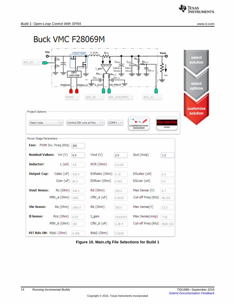
Figure 10. Main.cfg File Selections for Build 1
14 Running Incremental Builds TIDU986–September 2015Submit Documentation Feedback
Copyright © 2015, Texas Instruments Incorporated
www.ti.com Build 1: Open-Loop Control With SFRA
1.3.3 Build and Load the Project1. Click Clean Project. (If another build option exists, right-click on the project name.)2. Click Project.3. Click Build All.
4. Click . (The build 1 code should compile and load.)
NOTE: The CCS Debug icon in the upper right-hand corner indicates the Debug Perspective view.The program will stop at the start of main().
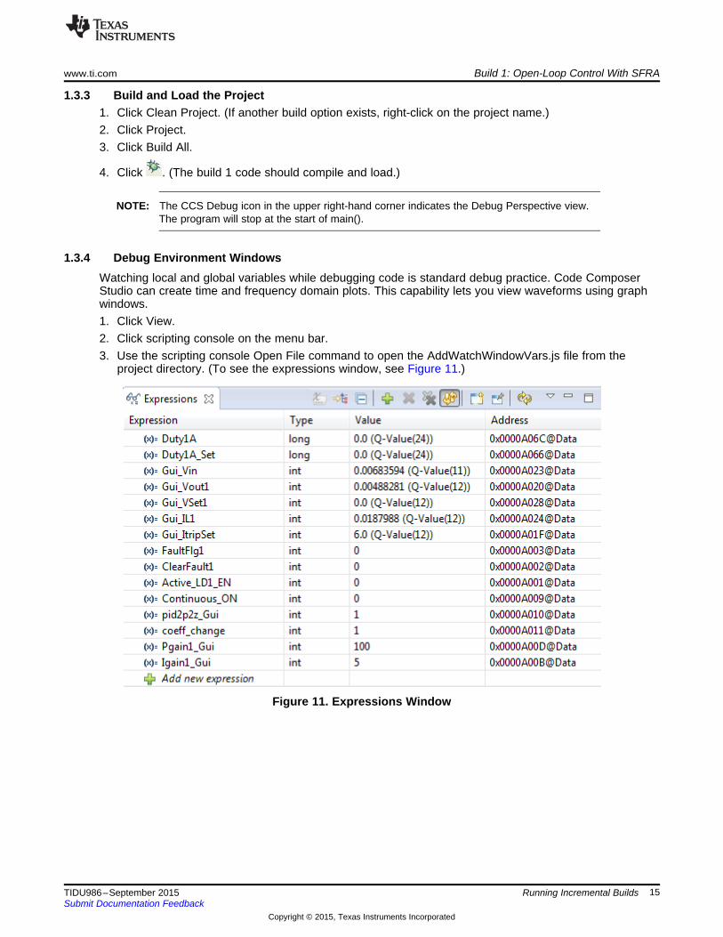
1.3.4 Debug Environment WindowsWatching local and global variables while debugging code is standard debug practice. Code ComposerStudio can create time and frequency domain plots. This capability lets you view waveforms using graphwindows.1. Click View.2. Click scripting console on the menu bar.3. Use the scripting console Open File command to open the AddWatchWindowVars.js file from the
project directory. (To see the expressions window, see Figure 11.)
Figure 11. Expressions Window
15TIDU986–September 2015 Running Incremental BuildsSubmit Documentation Feedback
Copyright © 2015, Texas Instruments Incorporated

Build 1: Open-Loop Control With SFRA www.ti.com
Table 4. Expressions Window Variable Description
Variable DescriptionQ24 is the value of duty input to PWMDRV_1ch. This is slewedDuty1A value based on Duty1A_Set. If used, SFRA signal is injected here.Q24 is the value of duty input. This value is set by the user in buildDuty1A_Set 1.
Gui_Vin This is the input voltage in volts (when displayed in Q11)Gui_Vout1 This is the output voltage in volts (when displayed in Q12)
This is the output voltage in volts set by user (when displayed inGui_VSet1 Q12). Not used in build 1.This is the instantaneous inductor current in amps (when displayedGui_IL1 in Q12.)This is the overcurrent shut-down level in amps (when displayed inGui_ItripSet Q12.)
FaultFlg1 This is the overcurrent PWM shut-down flag.ClearFault1 Clears fault flag and re-enable PWM.Active_LD1_EN Enables and disablse the active load feature.
When 1 is active, the load is permanently connected at the output.Continuous_ON When 0 is active, the load switches in and out of the circuit for
transient performance tests.Selects between loosely tuned PID-based compensator (0) andpid2p2z_Gui compensator designed using the Compensation Designer GUI (1).
coeff_change Calculates and updates coefficients.Pgain1_Gui This is the scaled (0–999) proportional gain value for PID.Igain1_Gui This is the scaled (0–999) integral gain value for PID.
1.3.5 Using Real-time EmulationReal-time emulation is a feature that lets windows within Code Composer Studio update while the MCU isrunning. This capability also lets you change variables or memory location values and have those changesaffect the MCU behavior by changing the voltage set-point, enabling the active load, and so forth. Thisability helps when tuning control law parameters on-the-fly.1. Enable real-time mode by hovering your mouse on the buttons on the horizontal toolbar
2. Click .3. If a message box appears, select YES to enable debug events.
NOTE: Selecting yes will set bit 1 (DGBM bit) of status register 1 (ST1) to 0. The DGBM is thedebug enable mask bit. When the DGBM bit is set to 0, memory and register values can bepassed to the host processor for updating the debugger windows.
4. Right-click in the expressions window.5. Select the Continuous Refresh Interval….
NOTE: When a large number of windows are open, the bandwidth over the emulation link is limited.Updating too many windows and variables in continuous refresh can cause the refreshfrequency to bog down. Slow down the refresh rate for the expressions window variables bychanging the continuous refresh interval (milliseconds) value to a rate of 1000 ms.
6. Click for the watch view.
16 Running Incremental Builds TIDU986–September 2015Submit Documentation Feedback
Copyright © 2015, Texas Instruments Incorporated
www.ti.com Build 1: Open-Loop Control With SFRA
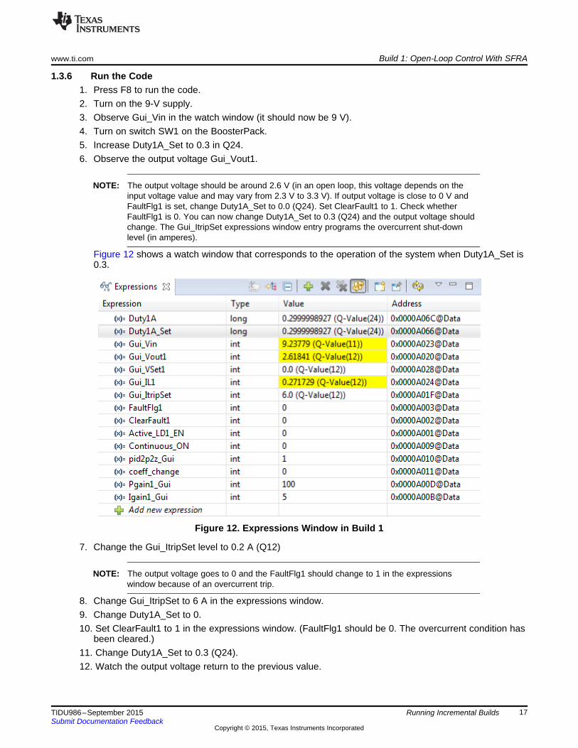
1.3.6 Run the Code1. Press F8 to run the code.2. Turn on the 9-V supply.3. Observe Gui_Vin in the watch window (it should now be 9 V).4. Turn on switch SW1 on the BoosterPack.5. Increase Duty1A_Set to 0.3 in Q24.6. Observe the output voltage Gui_Vout1.
NOTE: The output voltage should be around 2.6 V (in an open loop, this voltage depends on theinput voltage value and may vary from 2.3 V to 3.3 V). If output voltage is close to 0 V andFaultFlg1 is set, change Duty1A_Set to 0.0 (Q24). Set ClearFault1 to 1. Check whetherFaultFlg1 is 0. You can now change Duty1A_Set to 0.3 (Q24) and the output voltage shouldchange. The Gui_ItripSet expressions window entry programs the overcurrent shut-downlevel (in amperes).
Figure 12 shows a watch window that corresponds to the operation of the system when Duty1A_Set is0.3.
Figure 12. Expressions Window in Build 1
7. Change the Gui_ItripSet level to 0.2 A (Q12)
NOTE: The output voltage goes to 0 and the FaultFlg1 should change to 1 in the expressionswindow because of an overcurrent trip.
8. Change Gui_ItripSet to 6 A in the expressions window.9. Change Duty1A_Set to 0.10. Set ClearFault1 to 1 in the expressions window. (FaultFlg1 should be 0. The overcurrent condition has
been cleared.)11. Change Duty1A_Set to 0.3 (Q24).12. Watch the output voltage return to the previous value.
17TIDU986–September 2015 Running Incremental BuildsSubmit Documentation Feedback
Copyright © 2015, Texas Instruments Incorporated
Build 1: Open-Loop Control With SFRA www.ti.com
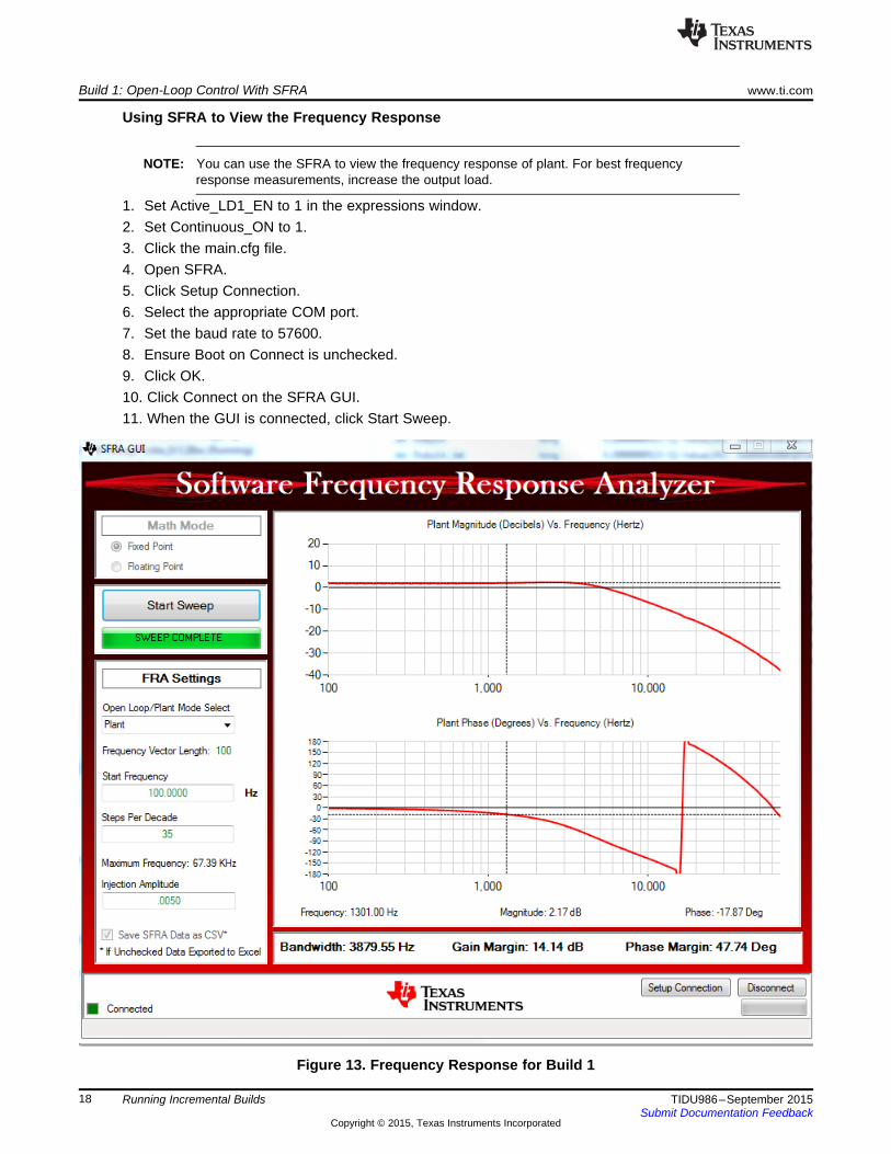
Using SFRA to View the Frequency Response
NOTE: You can use the SFRA to view the frequency response of plant. For best frequencyresponse measurements, increase the output load.
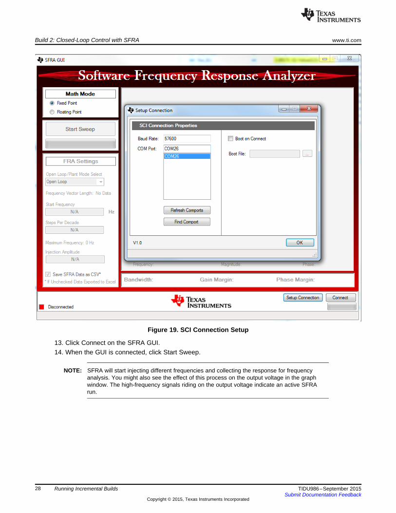
1. Set Active_LD1_EN to 1 in the expressions window.2. Set Continuous_ON to 1.3. Click the main.cfg file.4. Open SFRA.5. Click Setup Connection.6. Select the appropriate COM port.7. Set the baud rate to 57600.8. Ensure Boot on Connect is unchecked.9. Click OK.10. Click Connect on the SFRA GUI.11. When the GUI is connected, click Start Sweep.
Figure 13. Frequency Response for Build 1
18 Running Incremental Builds TIDU986–September 2015Submit Documentation Feedback
Copyright © 2015, Texas Instruments Incorporated
www.ti.com Build 2: Closed-Loop Control with SFRA
NOTE: SFRA will start injecting different frequencies and collecting the response for frequencyanalysis. When the frequency sweep completes the response displays on the SFRA GUI.
12. Close the SFRA GUI.
NOTE: You can change the Duty1A_Set value from the expressions window to ensure that theBoosterPack operates within its capabilities. Duty1A_Set has been restricted to a maximumvalue of 0.45 (Q24) in this build.
13. Turn off SW1 on the BoosterPack.14. Turn off the 9-V power supply.
Fully Halting the MCU in Real-time Mode1. Click on the toolbar to halt the processor.
2. Click to take the MCU out of real-time mode.3. Click Run.4. Click Reset.5. Click CPU Reset.
NOTE: Leave Code Composer Studio running for the next build or close CCS.
2 Build 2: Closed-Loop Control with SFRA
2.1 ObjectiveThe objective of this build is to regulate the output voltage of a buck power stage using closed-loopfeedback control realized in the form of a software-coded control loop. Use a compensator designed usingthe Compensation Designer GUI to achieve desired closed-loop performance. You can use SFRA GUIduring runtime to capture the frequency response of the system. An active-load circuit turned on by thesoftware provides a repetitive step change in the load to test the transient performance of the system intime-domain with the help of the CCS graph window.
2.2 OverviewThe software has been configured to provide closed-loop voltage control for the buck power stage. A 2-pole 2-zero controller block (CNTL_2P2Z) implements the control law. The output voltage feedbackAdc_Vout1 is an input to this block. The reference input to the CNTL_2P2Z block comes from the slewedoutput voltage command Vout_ref_wInj. If used, the SFRA signal is injected at the input of the controller.Similar to build 1, the controller output Duty1A must be connected to the PWMDRV_1ch block. You canadjust the output voltage command from the expressions window using the variable Gui_VSet1. Figure 14shows the system diagram for this build.
19TIDU986–September 2015 Running Incremental BuildsSubmit Documentation Feedback
Copyright © 2015, Texas Instruments Incorporated

Duty1AOutRef
Fdbk
CNTL_2P2Z:1:
Coef
B0B1B2A1A2
DminDmax
CNTL_2P2Z_CoefStruct
DBUFF
ADC
ADCDRV_1ch:1:
ADCDRV_1ch_Rlt VoutFB-1Adc_Vout1
Adc_Vout1
Vout_Ref_wInj PWMnA
PWMnB
PW
M
PWMDRV_1ch:n:
Duty
Period
200Khz200Khz
200Khz
Build 2: Closed-Loop Control with SFRA www.ti.com
Figure 14. System Diagram
Similar to build 1, the on-chip analog comparator (selected in the main.cfg file) and corresponding DACmechanism provide overcurrent protection (for the BoosterPack board this is COMP2). You can use theGui_ItripSet variable to set the reference trip level for the comparator. The comparator output is configuredto generate a one-shot trip action on the PWM module (selected in the main.cfg file) whenever the sensedcurrent is greater than the set limit. The flexibility of the trip mechanism on C2000 devices offers thepossibility to assign which actions should be taken by the PWM pin (set hi, set low, or set high-impedance) when specific trip events occur. In this project, EPWM4A and EPWM4B outputs are drivenlow immediately on a comparator event to protect the power stage.
The buck converter is driven with a 200 kHz PWM. The DPL_ISR_wFRA interrupt routine is triggered bythe selected PWM module. This interrupt calls the C-callable 20 assembly function DPL_Func. This iswhere the CNTL_2P2Z, PWMDRV_1ch and ADCDRV_1ch macros are executed.
Similar to build 1, a task state machine is part of the background code. Tasks are arranged in groups (A1,A2, A3…, B1, B2, B3…, C1, C2, C3…). Each group is executed according to three CPU timers which areconfigured with periods of 1 ms, 10 ms, and 100 ms, respectively. Within each group, each task is run in around-robin manner. For example, group B executes every 10 ms and group B has four tasks. Thecollective execution time for B1, B2, B3, and B4 tasks is 40 ms.
20 Running Incremental Builds TIDU986–September 2015Submit Documentation Feedback
Copyright © 2015, Texas Instruments Incorporated
www.ti.com Build 2: Closed-Loop Control with SFRA
2.3 Procedure
2.3.1 Hardware SetupFollow the steps listed under hardware setup section in the procedure from build 1.
2.3.2 Software SetupIf CCS is already open after completing build 1, skip to step 7.1. Open CCS.2. Navigate to View.3. Navigate to Resource Explorer.4. Navigate to controlSUITE.5. Navigate to English.6. Navigate to powerSUITE.7. Navigate to Development Kits.8. Navigate to Digital Power BoosterPack (BOOSTXL-BUCKCONV).9. Navigate to Example Projects.10. Navigate to Buck_VMC_F28069M (the demonstration).11. Click Import the example project into CCS.
NOTE: The Buck_VMC_F28069M project appears in the CCS Project Explorer window. This projectstarts to invoke all the necessary tools (for example, the compiler, the assembler, and thelinker) to build the project. A project contains all the files and build options needed to developan executable output file (.out) that can be run on the MCU hardware.
12. Click the arrow sign to the left of the project name13. Double-click main.cfg. (This file displays all the relevant device resources information, power stage
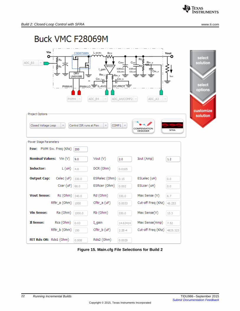
parameters, and project options.)14. Under Project Options, select Closed Voltage Loop. (See Figure 15.)
21TIDU986–September 2015 Running Incremental BuildsSubmit Documentation Feedback
Copyright © 2015, Texas Instruments Incorporated
Build 2: Closed-Loop Control with SFRA www.ti.com
Figure 15. Main.cfg File Selections for Build 2
22 Running Incremental Builds TIDU986–September 2015Submit Documentation Feedback
Copyright © 2015, Texas Instruments Incorporated

www.ti.com Build 2: Closed-Loop Control with SFRA
15. Click Compensation Designer.
NOTE: The Compensation Designer GUI uses the power stage model based on the data entered inthe main.cfg file and allows you to design compensators to achieve the closed-loopperformance you desire. Leave the default parameters for the designer.
16. Select the first compensator.
NOTE: This compensator is a 2-pole 2-zero compensator. When you select a new compensatorfrom the list, you update the magnitude and phase plots for the plant, open loop, andcompensator. These plots also update when you change the compensator. The defaultsoftware supports a 2-pole 2-zero compensator.
17. Note the bandwidth, gain margin, and phase margin for the default compensator 1.18. Close the Compensation Designer GUI.19. Using the default project options, save the main.cfg.
You are ready to build and load the project.
2.3.3 Build and Load the Project1. Click Project. (Alternatively, If another build option was built, right-click on the project name then click
Clean Project.)2. Click Build All.3. Watch the tools run in the build window.
4. Click . (Alternatively, click Run then click Debug.)
NOTE: The build 2 code compiles and loads. The CCS Debug icon in the upper right-hand cornerindicates you are in the Debug Perspective view. The program will stop at the start of main().
2.3.4 Debug Environment WindowsWatching local and global variables while debugging code is standard debug practice. Code ComposerStudio can create time and frequency domain plots. This capability lets you view waveforms using graphwindows.1. To populate the expressions window entries, click View.2. Click Scripting Console on the menu bar.
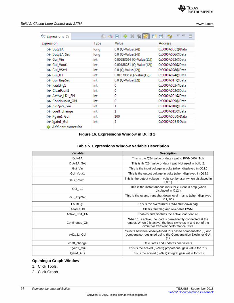
3. Open the AddWatchWindowVars.js file from the project directory using , the scripting consoleOpen File command.The expressions window should appear as shown in Figure 16.
23TIDU986–September 2015 Running Incremental BuildsSubmit Documentation Feedback
Copyright © 2015, Texas Instruments Incorporated
Build 2: Closed-Loop Control with SFRA www.ti.com
Figure 16. Expressions Window in Build 2
Table 5. Expressions Window Variable Description
Variable DescriptionDuty1A This is the Q24 value of duty input to PWMDRV_1ch.
Duty1A_Set This is th Q24 value of duty input. Not used in build 2.Gui_Vin This is the input voltage in volts (when displayed in Q11.)
Gui_Vout1 This is the output voltage in volts (when displayed in Q12.)This is the output voltage in volts set by user (when displayed inGui_VSet1 Q12.)
This is the instantaneous inductor current in amp (whenGui_IL1 displayed in Q12.)This is the overcurrent shut down level in amp (when displayedGui_ItripSet in Q12.)
FaultFlg1 This is the overcurrent PWM shut-down flag.ClearFault1 Clears fault flag and re-enable PWM.
Active_LD1_EN Enables and disables the active load feature.When 1 is active, the load is permanently connected at the
Continuous_ON output. When 0 is active, the load switches in and out of thecircuit for transient performance tests.
Selects between loosely-tuned PID based compensator (0) andpid2p2z_Gui compensator designed using the Compensation Designer GUI
(1).coeff_change Calculates and updates coefficients.Pgain1_Gui This is the scaled (0–999) proportional gain value for PID.Igain1_Gui This is the scaled (0–999) integral gain value for PID.
Opening a Graph Window1. Click Tools.2. Click Graph.
24 Running Incremental Builds TIDU986–September 2015Submit Documentation Feedback
Copyright © 2015, Texas Instruments Incorporated
www.ti.com Build 2: Closed-Loop Control with SFRA
3. Click Single Time.
NOTE: This creates a one time graph window to plot the data log buffer DBUFF1.
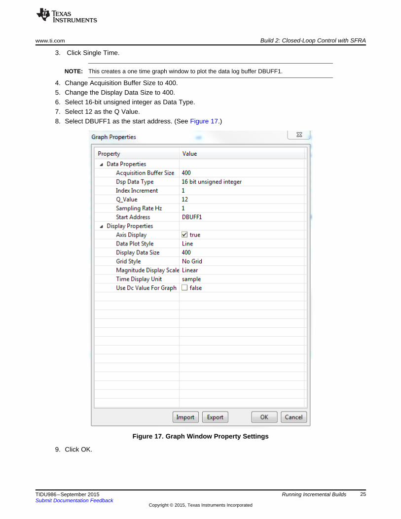
4. Change Acquisition Buffer Size to 400.5. Change the Display Data Size to 400.6. Select 16-bit unsigned integer as Data Type.7. Select 12 as the Q Value.8. Select DBUFF1 as the start address. (See Figure 17.)
Figure 17. Graph Window Property Settings
9. Click OK.
25TIDU986–September 2015 Running Incremental BuildsSubmit Documentation Feedback
Copyright © 2015, Texas Instruments Incorporated
Build 2: Closed-Loop Control with SFRA www.ti.com
2.3.5 Using Real-time EmulationReal-time emulation is a special emulation feature that lets windows within Code Composer Studio updatewhile the MCU is running. This feature lets graphs and watch windows update, while letting you changevariables or memory location values. The changes to variable and memory location values immediatelyaffect the MCU behavior. This feature is useful when tuning control law parameters on-the-fly.1. Hover the mouse over the icon on the horizontal toolbar.
2. Click .
NOTE: A message box may appear. If so, select YES to enable debug events. This sets bit 1(DGBM bit) of status register 1 (ST1) to 0.
The DGBM is the debug enable mask bit. When the DGBM bit is set to 0, memory and register valuescan be passed to the host processor for updating the debugger windows.When a large number of windows are open, as bandwidth over the emulation link is limited, updatingtoo many windows and variables in continuous refresh can cause the refresh frequency to bog down.(a) Right-click in the Expressions window.(b) Select the Continuous Refresh Interval….(c) Change the Continuous refresh interval (milliseconds) value to slow down the refresh rate for the
expressions window variables. (A rate of 1000 ms is typical.)
(d) Click in the graph window.
(e) Click in the expressions window.
2.3.6 Run the Code1. Press F8. (Alternatively, click Run.)2. Turn on the 9-V supply.3. Observe that the Gui_Vin value is approximately 9 V in the watch window.4. Turn on switch SW1 on the BoosterPack.
NOTE: If this is the first time SW1 has been turned on since a device reset, the output voltage(Gui_Vout1) ramps up to 2 V.
If not, change Gui_VSet1 to 2.0 (Q12).
If output voltage does not ramp up to 2 V and FaultFlg1 is Set, do the following:(a) Change Gui_VSet1 to 0.0 (Q12).(b) Set ClearFault1 to 1. (FaultFlg1 should be 0.)(c) Change Gui_VSet1 to 2.0 (Q12). (The output voltage should change from 0 V to 2 V. See
Figure 18.)
26 Running Incremental Builds TIDU986–September 2015Submit Documentation Feedback
Copyright © 2015, Texas Instruments Incorporated

www.ti.com Build 2: Closed-Loop Control with SFRA
Figure 18. Expressions Window in Build 2
5. To get good frequency response measurements, set Active_LD1_EN to 1 in the expressions window.6. Set Continuous_ON to 1. (The output voltage should still be regulated at 2 V.)7. Click the main.cfg file.8. Open SFRA.9. Click Setup Connection.10. Select the appropriate COM port.11. Ensure that Boot on Connect is unchecked.12. Click OK.
27TIDU986–September 2015 Running Incremental BuildsSubmit Documentation Feedback
Copyright © 2015, Texas Instruments Incorporated
Build 2: Closed-Loop Control with SFRA www.ti.com
Figure 19. SCI Connection Setup
13. Click Connect on the SFRA GUI.14. When the GUI is connected, click Start Sweep.
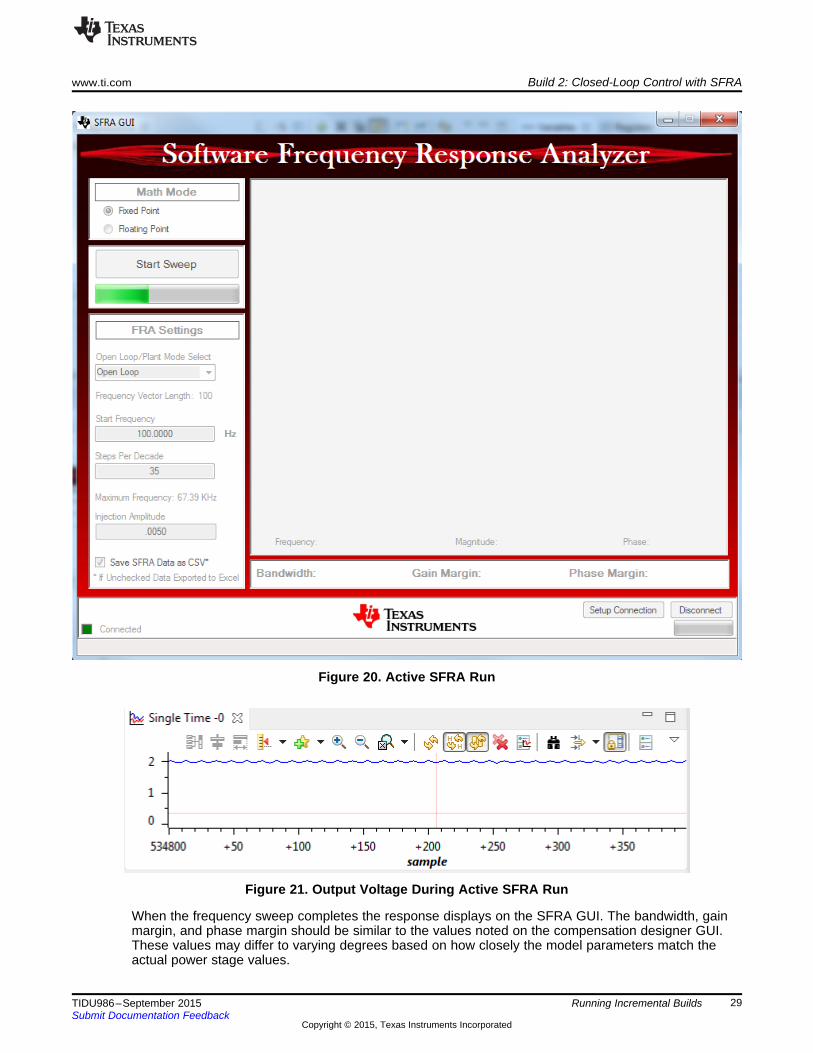
NOTE: SFRA will start injecting different frequencies and collecting the response for frequencyanalysis. You might also see the effect of this process on the output voltage in the graphwindow. The high-frequency signals riding on the output voltage indicate an active SFRArun.
28 Running Incremental Builds TIDU986–September 2015Submit Documentation Feedback
Copyright © 2015, Texas Instruments Incorporated
www.ti.com Build 2: Closed-Loop Control with SFRA
Figure 20. Active SFRA Run
Figure 21. Output Voltage During Active SFRA Run
When the frequency sweep completes the response displays on the SFRA GUI. The bandwidth, gainmargin, and phase margin should be similar to the values noted on the compensation designer GUI.These values may differ to varying degrees based on how closely the model parameters match theactual power stage values.
29TIDU986–September 2015 Running Incremental BuildsSubmit Documentation Feedback
Copyright © 2015, Texas Instruments Incorporated

Build 2: Closed-Loop Control with SFRA www.ti.com
Figure 22. Frequency Response for Build 2
15. Close the SFRA GUI.16. Set Continuous_ON to 0.17. Change pid2p2z_Gui to 0.18. Set coeff_change to 1.
NOTE: Changing pid2p2zz_Gui to 0 and setting coeff_change to 1 change the compensator fromthe compensator designed using the Compensation Designer GUI to a loosely tuned PID-based compensator that has been manually tuned using Pgain1_Gui and Igain1_Gui.
19. Zoom-in on the output voltage transients on the graph window. (The output voltage spikes wheneverthe active load is turned on and off.)
30 Running Incremental Builds TIDU986–September 2015Submit Documentation Feedback
Copyright © 2015, Texas Instruments Incorporated

www.ti.com Build 3: Closed-Loop Control Without SFRA
Figure 23. Transient Response Obtained Using Loosely Tuned Coefficients
20. Change pid2p2z_Gui to 1.21. Set coeff_change to 1.22. Return to the original compensator from the Compensation Designer GUI. (The output voltage spikes
voltage transients have reduced. See Figure 24.)
Figure 24. Transient Response Obtained Using Compensation Designer GUI Coefficients
The reduced spikes in the output voltage verifies the improved transient performance of the system intime-domain.
23. Turn off SW1 on the BoosterPack.24. Turn off the 9-V power supply.
25. Click on the toolbar to halt the processor. (Alternatively, to halt the processor, click Run then .)
26. Click to take the MCU out of real-time mode.27. Click Run.28. Click Reset.29. Click CPU reset. (Leave Code Composer Studio running for the next build or close CCS.)
3 Build 3: Closed-Loop Control Without SFRAThis build option is similar to build 2 but runs without SFRA. This omission provides a method to controlthe system without the additional run-time SFRA software. To run this build, follow the steps in build 2.The SFRA tool may not be used with this build.
31TIDU986–September 2015 Running Incremental BuildsSubmit Documentation Feedback
Copyright © 2015, Texas Instruments Incorporated
TIDU986–September 2015
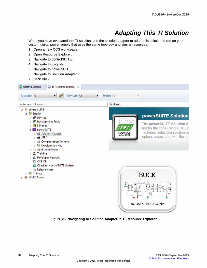
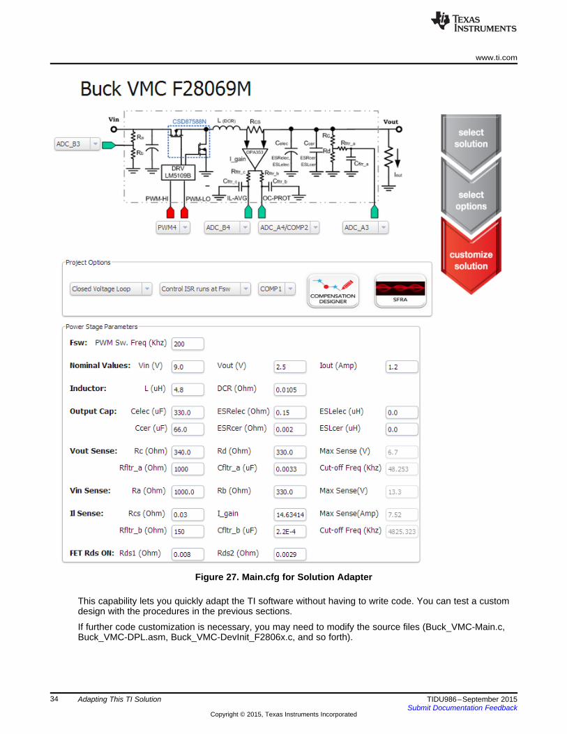
Adapting This TI SolutionWhen you have evaluated this TI solution, use the solution adapter to adapt this solution to run on yourcustom digital power supply that uses the same topology and similar resources.1. Open a new CCS workspace.2. Open Resource Explorer.3. Navigate to controlSUITE.4. Navigate to English.5. Navigate to powerSUITE.6. Navigate to Solution Adapter.7. Click Buck.
Figure 25. Navigating to Solution Adapter in TI Resource Explorer
32 Adapting This TI Solution TIDU986–September 2015Submit Documentation Feedback
Copyright © 2015, Texas Instruments Incorporated
www.ti.com
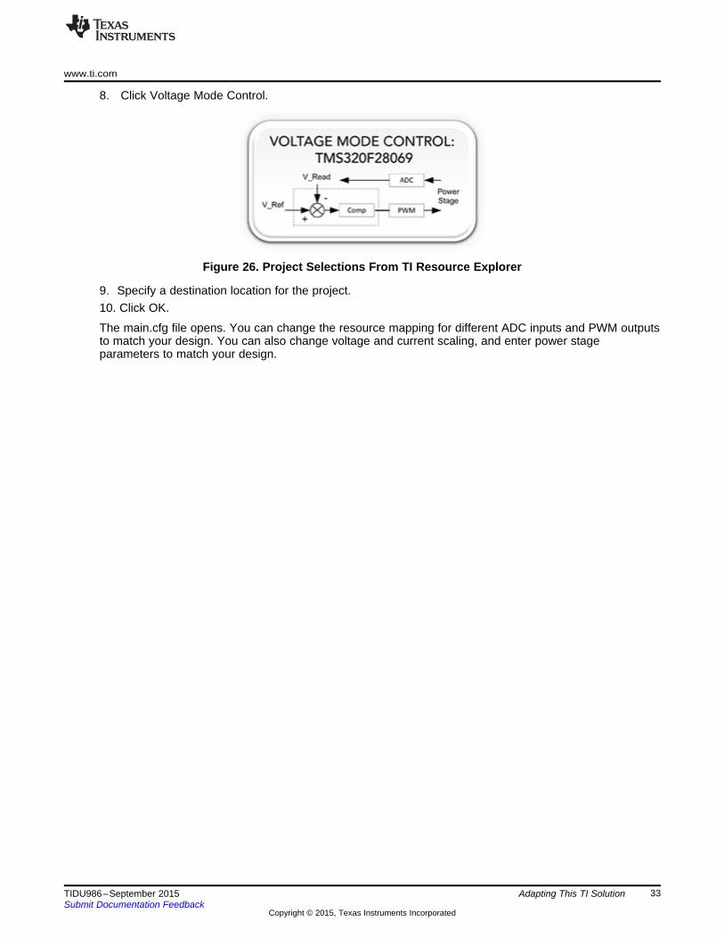
8. Click Voltage Mode Control.
Figure 26. Project Selections From TI Resource Explorer
9. Specify a destination location for the project.10. Click OK.
The main.cfg file opens. You can change the resource mapping for different ADC inputs and PWM outputsto match your design. You can also change voltage and current scaling, and enter power stageparameters to match your design.
33TIDU986–September 2015 Adapting This TI SolutionSubmit Documentation Feedback
Copyright © 2015, Texas Instruments Incorporated
www.ti.com
Figure 27. Main.cfg for Solution Adapter
This capability lets you quickly adapt the TI software without having to write code. You can test a customdesign with the procedures in the previous sections.
If further code customization is necessary, you may need to modify the source files (Buck_VMC-Main.c,Buck_VMC-DPL.asm, Buck_VMC-DevInit_F2806x.c, and so forth).
34 Adapting This TI Solution TIDU986–September 2015Submit Documentation Feedback
Copyright © 2015, Texas Instruments Incorporated

IMPORTANT NOTICE FOR TI REFERENCE DESIGNS
Texas Instruments Incorporated ("TI") reference designs are solely intended to assist designers (“Buyers”) who are developing systems thatincorporate TI semiconductor products (also referred to herein as “components”). Buyer understands and agrees that Buyer remainsresponsible for using its independent analysis, evaluation and judgment in designing Buyer’s systems and products.TI reference designs have been created using standard laboratory conditions and engineering practices. TI has not conducted anytesting other than that specifically described in the published documentation for a particular reference design. TI may makecorrections, enhancements, improvements and other changes to its reference designs.Buyers are authorized to use TI reference designs with the TI component(s) identified in each particular reference design and to modify thereference design in the development of their end products. HOWEVER, NO OTHER LICENSE, EXPRESS OR IMPLIED, BY ESTOPPELOR OTHERWISE TO ANY OTHER TI INTELLECTUAL PROPERTY RIGHT, AND NO LICENSE TO ANY THIRD PARTY TECHNOLOGYOR INTELLECTUAL PROPERTY RIGHT, IS GRANTED HEREIN, including but not limited to any patent right, copyright, mask work right,or other intellectual property right relating to any combination, machine, or process in which TI components or services are used.Information published by TI regarding third-party products or services does not constitute a license to use such products or services, or awarranty or endorsement thereof. Use of such information may require a license from a third party under the patents or other intellectualproperty of the third party, or a license from TI under the patents or other intellectual property of TI.TI REFERENCE DESIGNS ARE PROVIDED "AS IS". TI MAKES NO WARRANTIES OR REPRESENTATIONS WITH REGARD TO THEREFERENCE DESIGNS OR USE OF THE REFERENCE DESIGNS, EXPRESS, IMPLIED OR STATUTORY, INCLUDING ACCURACY ORCOMPLETENESS. TI DISCLAIMS ANY WARRANTY OF TITLE AND ANY IMPLIED WARRANTIES OF MERCHANTABILITY, FITNESSFOR A PARTICULAR PURPOSE, QUIET ENJOYMENT, QUIET POSSESSION, AND NON-INFRINGEMENT OF ANY THIRD PARTYINTELLECTUAL PROPERTY RIGHTS WITH REGARD TO TI REFERENCE DESIGNS OR USE THEREOF. TI SHALL NOT BE LIABLEFOR AND SHALL NOT DEFEND OR INDEMNIFY BUYERS AGAINST ANY THIRD PARTY INFRINGEMENT CLAIM THAT RELATES TOOR IS BASED ON A COMBINATION OF COMPONENTS PROVIDED IN A TI REFERENCE DESIGN. IN NO EVENT SHALL TI BELIABLE FOR ANY ACTUAL, SPECIAL, INCIDENTAL, CONSEQUENTIAL OR INDIRECT DAMAGES, HOWEVER CAUSED, ON ANYTHEORY OF LIABILITY AND WHETHER OR NOT TI HAS BEEN ADVISED OF THE POSSIBILITY OF SUCH DAMAGES, ARISING INANY WAY OUT OF TI REFERENCE DESIGNS OR BUYER’S USE OF TI REFERENCE DESIGNS.TI reserves the right to make corrections, enhancements, improvements and other changes to its semiconductor products and services perJESD46, latest issue, and to discontinue any product or service per JESD48, latest issue. Buyers should obtain the latest relevantinformation before placing orders and should verify that such information is current and complete. All semiconductor products are soldsubject to TI’s terms and conditions of sale supplied at the time of order acknowledgment.TI warrants performance of its components to the specifications applicable at the time of sale, in accordance with the warranty in TI’s termsand conditions of sale of semiconductor products. Testing and other quality control techniques for TI components are used to the extent TIdeems necessary to support this warranty. Except where mandated by applicable law, testing of all parameters of each component is notnecessarily performed.TI assumes no liability for applications assistance or the design of Buyers’ products. Buyers are responsible for their products andapplications using TI components. To minimize the risks associated with Buyers’ products and applications, Buyers should provideadequate design and operating safeguards.Reproduction of significant portions of TI information in TI data books, data sheets or reference designs is permissible only if reproduction iswithout alteration and is accompanied by all associated warranties, conditions, limitations, and notices. TI is not responsible or liable forsuch altered documentation. Information of third parties may be subject to additional restrictions.Buyer acknowledges and agrees that it is solely responsible for compliance with all legal, regulatory and safety-related requirementsconcerning its products, and any use of TI components in its applications, notwithstanding any applications-related information or supportthat may be provided by TI. Buyer represents and agrees that it has all the necessary expertise to create and implement safeguards thatanticipate dangerous failures, monitor failures and their consequences, lessen the likelihood of dangerous failures and take appropriateremedial actions. Buyer will fully indemnify TI and its representatives against any damages arising out of the use of any TI components inBuyer’s safety-critical applications.In some cases, TI components may be promoted specifically to facilitate safety-related applications. With such components, TI’s goal is tohelp enable customers to design and create their own end-product solutions that meet applicable functional safety standards andrequirements. Nonetheless, such components are subject to these terms.No TI components are authorized for use in FDA Class III (or similar life-critical medical equipment) unless authorized officers of the partieshave executed an agreement specifically governing such use.Only those TI components that TI has specifically designated as military grade or “enhanced plastic” are designed and intended for use inmilitary/aerospace applications or environments. Buyer acknowledges and agrees that any military or aerospace use of TI components thathave not been so designated is solely at Buyer's risk, and Buyer is solely responsible for compliance with all legal and regulatoryrequirements in connection with such use.TI has specifically designated certain components as meeting ISO/TS16949 requirements, mainly for automotive use. In any case of use ofnon-designated products, TI will not be responsible for any failure to meet ISO/TS16949.IMPORTANT NOTICE
Mailing Address: Texas Instruments, Post Office Box 655303, Dallas, Texas 75265Copyright © 2015, Texas Instruments Incorporated